CN101792109A - Micro inertial sensor with transversely movable electrodes embedded and manufacturing method thereof - Google Patents
Micro inertial sensor with transversely movable electrodes embedded and manufacturing method thereofDownload PDFInfo
- Publication number
- CN101792109A CN101792109ACN 201010125451CN201010125451ACN101792109ACN 101792109 ACN101792109 ACN 101792109ACN 201010125451CN201010125451CN 201010125451CN 201010125451 ACN201010125451 ACN 201010125451ACN 101792109 ACN101792109 ACN 101792109A
- Authority
- CN
- China
- Prior art keywords
- sensor
- mass
- electrode
- comb
- grid
- Prior art date
- Legal status (The legal status is an assumption and is not a legal conclusion. Google has not performed a legal analysis and makes no representation as to the accuracy of the status listed.)
- Granted
Links
Images


Landscapes
- Pressure Sensors (AREA)
Abstract
Translated fromChinese
Description
Translated fromChinese技术领域technical field
本发明属于微电子机械技术领域,涉及一种微惯性传感器,具体涉及一种可变电容极板的相对运动表现为滑膜阻尼、振子上嵌入了横向可动电极的高分辨率微惯性传感器及其制作方法。The invention belongs to the field of micro-electromechanical technology, and relates to a micro-inertial sensor, in particular to a high-resolution micro-inertial sensor in which the relative motion of a variable capacitance plate is represented by synovial film damping, and a transverse movable electrode is embedded on a vibrator. its production method.
背景技术Background technique
最近十几年来,用微机械技术制作的加速度计得到了迅速的发展。其主要的加速度检测技术有压阻检测、压电检测、热检测、共振检测、电磁检测、光检测、隧道电流检测和电容检测等。此外,还有一些基于别的检测技术的加速度计,如光加速度计、电磁加速度计、电容加速度计等。光加速度计的发展主要是为了结合光和微机械的优点,制作高电磁屏蔽或者好线性度的传感器。在这些传感器中,电容式加速度传感器,由于具有温度系数小,灵敏度高,稳定性好等优点,是目前研制地最多的一类加速度传感器。微机械电容式传感器的制作方法有表面微机械加工方法和体硅微机械加工方法。采用表面微机械加工工艺可以和集成电路工艺兼容,从而集成传感器的外围电路,成本低,但是传感器的噪声大、稳定性差,量程和带宽小。采用体硅微机械加工工艺可以提高传感器芯片的质量,从而降低噪声,改善稳定性,提高灵敏度。缺点是体积稍大,但可以制作出超高精度的微机械惯性传感器。为了得到较高的测量灵敏度和减小外围电路的复杂性,可以通过增加传感器振子的质量和增大传感器的静态测试电容的方法,从而减小机械噪声和电路噪声。而对于用体硅工艺如深反应粒子刻蚀(Deep RIE)加工的梳齿状的电容式传感器,其极板电容的深宽比一般小于27∶1,这就限制了传感器振子的质量增加和电容极板间距的减小。而对于小间距极板电容,其压膜空气阻尼较大,增大了传感器的机械噪声,减小该机械噪声可以通过在极板上刻蚀阻尼条,或把电容改为变面积的方式,使阻尼表现为滑膜阻尼,而减小电路噪声的方法之一便是通过增大检测电容。In recent ten years, accelerometers made with micromechanical technology have been developed rapidly. Its main acceleration detection technologies include piezoresistive detection, piezoelectric detection, thermal detection, resonance detection, electromagnetic detection, light detection, tunnel current detection and capacitance detection. In addition, there are accelerometers based on other detection technologies, such as optical accelerometers, electromagnetic accelerometers, and capacitive accelerometers. The development of optical accelerometers is mainly to combine the advantages of light and micromechanics to make sensors with high electromagnetic shielding or good linearity. Among these sensors, the capacitive acceleration sensor is the most widely developed type of acceleration sensor due to its small temperature coefficient, high sensitivity, and good stability. The fabrication methods of micromachined capacitive sensors include surface micromachining methods and bulk silicon micromachining methods. The surface micromachining process can be compatible with the integrated circuit process, so that the peripheral circuit of the sensor is integrated, and the cost is low, but the sensor has large noise, poor stability, and small range and bandwidth. The use of bulk silicon micromachining processes can improve the quality of the sensor chip, thereby reducing noise, improving stability, and increasing sensitivity. The disadvantage is that the volume is slightly larger, but ultra-high-precision micro-mechanical inertial sensors can be produced. In order to obtain higher measurement sensitivity and reduce the complexity of the peripheral circuit, the mechanical noise and circuit noise can be reduced by increasing the quality of the sensor vibrator and increasing the static test capacitance of the sensor. For comb-shaped capacitive sensors processed by bulk silicon technology such as deep reactive particle etching (Deep RIE), the aspect ratio of the plate capacitance is generally less than 27:1, which limits the increase in the mass of the sensor vibrator and the Reduction of capacitor plate spacing. For small-pitch plate capacitors, the pressure film air damping is relatively large, which increases the mechanical noise of the sensor. The mechanical noise can be reduced by etching damping strips on the plate, or changing the capacitor to a variable-area method. One way to make the damping appear as synovial damping, and to reduce circuit noise, is by increasing the sense capacitor.
发明内容Contents of the invention
本发明的目的在于提供一种可变电容的相对运动表现为滑膜阻尼、振子上嵌入了横向可动电极的高分辨率微惯性传感器及其制作方法,以制作工艺简单、灵敏度高、噪声小的电容式微惯性传感器。The purpose of the present invention is to provide a high-resolution micro-inertial sensor whose relative motion of the variable capacitor is represented by synovial film damping, and a transverse movable electrode is embedded on the vibrator, and its manufacturing method, with simple manufacturing process, high sensitivity and low noise capacitive micro-inertial sensor.
本发明提供的电容式微惯性传感器包括第一基板及其上表面的检测用交叉梳齿状固定对电极、固定于第一基板上的敏感器锚点、固定质量块锚点、第二基板的悬于第一基板上方的可沿纵向运动的敏感器栅质量块、将敏感器锚点和敏感器栅质量块相连的U形敏感器支撑梁、敏感器可横向移动质量块、将敏感器可横向移动质量快和敏感器栅质量块相连的U形敏感器连接梁、固定质量块上的梳形固定电极、敏感器外部引出电极、U形敏感器支撑梁、电绝缘层、驱动导线和驱动导线引出电极。The capacitive micro-inertial sensor provided by the present invention includes a first substrate and a cross-comb-shaped fixed counter electrode for detection on its upper surface, a sensor anchor point fixed on the first substrate, a fixed mass anchor point, and a suspension of the second substrate. The sensor grid mass that can move longitudinally above the first substrate, the U-shaped sensor support beam that connects the sensor anchor point and the sensor grid mass, the sensor can move the mass block laterally, and the sensor can move laterally The U-shaped sensor connecting beam with fast moving mass connected to the grid mass of the sensor, the comb-shaped fixed electrode on the fixed mass, the external lead-out electrode of the sensor, the U-shaped sensor support beam, the electrical insulation layer, the driving wire and the driving wire Extract the electrodes.
所述的敏感器栅质量块是由纵向等间距、横向平行的栅形电极、连接栅形电极的边框及敏感器栅质量块矩形凸起组成,敏感器栅质量块矩形凸起有两个且沿着敏感器栅质量块的横向中心线位于敏感器栅质量块两侧。The sensor grid mass is composed of vertically equidistant grid electrodes, horizontally parallel grid electrodes, a frame connecting the grid electrodes, and a rectangular protrusion of the sensor grid mass. The sensor grid mass rectangular protrusions have two and Along the transverse centerline of the sensor grid mass, it is located on both sides of the sensor grid mass.
所述的敏感器可横向移动质量块有两个,分别位于敏感器栅质量块的两侧,由矩形块、梳形可动电极和敏感器可横向移动质量块矩形凸起组成,其纵向长度和敏感器栅质量块的主体长度相同;敏感器可横向移动质量块矩形凸起和敏感器栅质量块矩形凸起相对,形成电容调整间隙。每个敏感器可横向移动质量块和敏感器栅质量块通过两根位于敏感器可横向移动质量块和敏感器栅质量块之间的U形敏感器连接梁相连,该两根U形敏感器连接梁沿着敏感器栅质量块的横向中心线对称设置,该两根U形敏感器连接梁沿着敏感器栅质量块的纵向中心线与位于敏感器栅质量块另一侧的另两根U形敏感器连接梁对应对称设置,实现敏感器可横向移动质量块的横向敏感。所述的每根敏感器连接梁始于矩形块的一角,终于敏感器栅质量块的边框的对应角,其U形靠近敏感器栅质量块的横向中心线。There are two laterally movable mass blocks of the sensor, which are respectively located on both sides of the mass block of the sensor grid, and are composed of a rectangular block, a comb-shaped movable electrode and a rectangular protrusion of the laterally movable mass block of the sensor. The length of the body is the same as that of the grid quality block of the sensor; the rectangular protrusion of the movable mass block of the sensor is opposite to the rectangular protrusion of the grid mass block of the sensor, forming a capacitance adjustment gap. Each sensor movable mass and sensor grid mass are connected by two U-shaped sensor connecting beams located between the sensor movable mass and the sensor grid mass. The two U-shaped sensor The connecting beams are arranged symmetrically along the transverse centerline of the sensor grid mass, and the two U-shaped sensor connecting beams are connected to the other two on the other side of the sensor grid mass along the longitudinal centerline The connecting beams of the U-shaped sensor are correspondingly arranged symmetrically, so as to realize the lateral sensitivity of the laterally movable mass block of the sensor. Each sensor connecting beam starts from a corner of the rectangular block and ends at the corresponding corner of the frame of the sensor grid mass, and its U shape is close to the transverse centerline of the sensor grid mass.
所述的梳形可动电极由n个等间距的梳齿和连接梳齿的矩形条组成,n≥1,梳齿与矩形条垂直设置;梳形可动电极在矩形块的外侧分别对应组成两组硅条组,每组硅条组分别对应设置在矩形块的相应处,每组硅条组包括平行设置的m条梳形可动电极,m≥2,连接梳齿的矩形条与矩形块侧边垂直设置。The comb-shaped movable electrode is composed of n equally spaced comb teeth and rectangular strips connecting the comb teeth, n≥1, the comb teeth and the rectangular strips are arranged vertically; the comb-shaped movable electrodes are respectively formed on the outside of the rectangular block Two groups of silicon strips, each group of silicon strips is arranged at the corresponding position of the rectangular block, each group of silicon strips includes m comb-shaped movable electrodes arranged in parallel, m≥2, connecting the rectangular strips of the comb teeth and the rectangular The block sides are set vertically.
矩形块一侧每组的梳形可动电极沿敏感器质量块的横向中心线对称设置;边框两侧的四组硅条组,每组梳形可动电极沿敏感器质量块的纵向中心线对应对称设置。Each group of comb-shaped movable electrodes on one side of the rectangular block is arranged symmetrically along the transverse centerline of the sensor mass; four groups of silicon strips on both sides of the frame, each group of comb-shaped movable electrodes is arranged along the longitudinal centerline of the sensor mass Corresponds to symmetrical settings.
所述的敏感器锚点沿敏感器栅质量块的纵向中心线分别设置在敏感器栅质量块的两端,并通过敏感器支撑梁与敏感器栅质量块连接,敏感器外部引出电极设置在一个敏感器锚点上。The anchor points of the sensor are respectively arranged at both ends of the sensor grid mass along the longitudinal centerline of the sensor grid mass, and are connected to the sensor grid mass through the sensor support beam, and the external lead electrodes of the sensor are arranged at on a sensor anchor.
所述的固定质量块与每组硅条组一一对应设置,每个固定质量块包括固定质量块锚点和梳形固定电极。梳形固定电极设置在与硅条组对应的一侧,共有m条,梳形固定电极外形和梳形可动电极相同。梳形可动电极和梳形固定电极的位置对应设置,梳形固定电极的梳齿与梳形可动电极的梳齿对应交叉设置。The fixed mass blocks are provided in one-to-one correspondence with each silicon strip group, and each fixed mass block includes a fixed mass block anchor point and a comb-shaped fixed electrode. The comb-shaped fixed electrodes are arranged on the side corresponding to the group of silicon strips, and there are m strips in total. The appearance of the comb-shaped fixed electrodes is the same as that of the comb-shaped movable electrodes. The positions of the comb-shaped movable electrode and the comb-shaped fixed electrode are arranged correspondingly, and the comb teeth of the comb-shaped fixed electrode and the comb-shaped movable electrode are correspondingly arranged to intersect.
所述的驱动导线共有两根,分别纵向设置于相应的矩形块上,每根驱动导线的一端通过沿对应的敏感器连接梁、边框端和敏感器支撑梁上所铺设的金属导线与对应的驱动导线引出电极连接。在驱动导线、金属导线、驱动导线引出电极组成的金属层与矩形块对应部分之间设置有电绝缘层。There are two driving wires, which are respectively vertically arranged on the corresponding rectangular blocks. One end of each driving wire is connected to the corresponding metal wire laid on the corresponding sensor connecting beam, frame end and sensor supporting beam. The drive leads lead out to the electrode connections. An electric insulating layer is arranged between the metal layer composed of the driving wire, the metal wire, the driving wire lead-out electrode and the corresponding part of the rectangular block.
所述的电容调整间隙比对应梳形可动电极和梳形固定电极上的对应梳齿间的横向间距小一微米以上。The capacitance adjustment gap is more than one micron smaller than the transverse spacing between the corresponding comb-shaped movable electrode and the corresponding comb-shaped fixed electrode.
所述的检测用交叉梳齿状固定对电极由沿横向相对交叉的梳齿电极和引出电极组成,各相邻梳齿电极间的间隙不小于一微米,交叉的梳齿电极对应组成梳齿电极对。The cross-comb-shaped fixed counter electrode for detection is composed of comb-teeth electrodes and lead-out electrodes that cross relative to each other in the transverse direction, the gap between each adjacent comb-teeth electrodes is not less than one micron, and the intersecting comb-teeth electrodes correspond to form comb-teeth electrodes right.
所述的栅形电极位于对应的梳齿电极对的正上方。The grid-shaped electrodes are located directly above the corresponding pair of comb-teeth electrodes.
制作该微惯性传感器的具体步骤是:The specific steps of making the micro inertial sensor are:
(1)在第一基板的上表面形成检测用交叉梳齿状固定对电极;(1) Forming a cross-comb-shaped fixed counter electrode for detection on the upper surface of the first substrate;
(2)在第二基板的上表面形成电绝缘层;(2) forming an electrical insulation layer on the upper surface of the second substrate;
(3)在第二基板的下表面形成悬浮区;(3) forming a suspension area on the lower surface of the second substrate;
(4)在第二基板的下表面的所述悬浮区形成悬浮间距;(4) forming a suspension distance in the suspension area on the lower surface of the second substrate;
(5)将所述第一基板的上表面与所述第二基板的下表面相向键合,所述检测用交叉梳齿状固定对电极和悬浮区互相对准,形成栅形电极下表面与检测用交叉梳齿状固定对电极的上表面的间隙;(5) The upper surface of the first substrate is bonded to the lower surface of the second substrate, and the interdigitated fixed counter electrode for detection and the suspension area are aligned with each other to form the lower surface of the grid-shaped electrode and the lower surface of the second substrate. Detect the gap between the upper surface of the fixed counter electrode with cross-comb teeth;
(6)刻蚀所述第二基板上的绝缘层,形成驱动导线、金属导线、驱动导线引出电极组成的金属层与矩形块对应部分之间的电绝缘层。(6) Etching the insulating layer on the second substrate to form an electrical insulating layer between the metal layer composed of the driving wire, the metal wire, and the driving wire lead-out electrode and the corresponding part of the rectangular block.
(7)在电绝缘层上形成驱动导线、金属导线、驱动导线引出电极组,同时在敏感器锚点上形成敏感器外部引出电极;(7) Forming a driving wire, a metal wire, and a driving wire lead-out electrode group on the electrical insulating layer, and simultaneously forming an external lead-out electrode of the sensor on the anchor point of the sensor;
(8)刻蚀所述第二基板,形成固定于第一基板上的敏感器锚点、固定质量块锚点、悬于第一基板上方的可沿纵向运动的敏感器栅质量块、将敏感器锚点和敏感器栅质量块相连的U形敏感器支撑梁、敏感器可横向移动质量快、将敏感器可横向移动质量快和敏感器栅质量块相连的U形敏感器连接梁、固定质量块上的梳齿固定电极。(8) Etching the second substrate to form the anchor point of the sensor fixed on the first substrate, the anchor point of the fixed mass, the sensor grid mass suspended above the first substrate and movable in the longitudinal direction, and the sensitive The U-shaped sensor support beam connecting the anchor point of the sensor with the grid mass of the sensor, the fast moving mass of the sensor, the U-shaped sensor connecting beam connecting the fast moving mass of the sensor with the grid mass of the sensor, and the fixed Comb teeth on the proof mass hold the electrodes.
综上所述,根据本发明方法可以实现由第一基板及其上表面的检测用交叉梳齿状固定对电极、固定于第一基板上的敏感器锚点、固定质量块锚点、第二基板的悬于第一基板上方的可沿纵向运动的敏感器栅质量块、将敏感器锚点和敏感器栅质量块相连的U形敏感器支撑梁、敏感器可横向移动质量快、将敏感器可横向移动质量快和敏感器栅质量块相连的U形敏感器连接梁、固定质量块上的梳形固定电极、敏感器外部引出电极、U形敏感器支撑梁和U形敏感器连接梁上的电绝缘层、驱动导线和驱动导线引出电极及其他金属导线连接部位下的电绝缘层、电绝缘层上的驱动导线和驱动导线引出电极组成的微惯性传感器。第二基板上形成的栅形电极与第一基板上的梳齿电极对互相对准。栅形电极的下表面与第一基板上的交叉梳齿状固定对电极之间起主要作用的是滑膜阻尼。梳形可动电极和梳形固定电极上的对应梳齿之间起主要作用的也是滑膜阻尼,滑膜阻尼要远小于压模阻尼,因而微传感器的机械噪声得到改善。In summary, according to the method of the present invention, the first substrate and the cross-comb-shaped fixed counter electrode for detection on the upper surface thereof, the anchor point of the sensor fixed on the first substrate, the anchor point of the fixed mass, the second The sensor grid mass that can move longitudinally above the substrate is suspended above the first substrate, the U-shaped sensor support beam that connects the anchor point of the sensor with the sensor grid mass, and the sensor can move laterally quickly. The U-shaped sensor connecting beam that can move the mass fast and the sensor grid mass, the comb-shaped fixed electrode on the fixed mass, the external lead-out electrode of the sensor, the U-shaped sensor support beam and the U-shaped sensor connecting beam A micro-inertial sensor composed of an electrical insulation layer on the upper surface, a driving wire and the electrode leading out of the driving wire, and an electrical insulating layer under the connecting parts of other metal wires, a driving wire on the electrical insulating layer, and the electrode drawn out of the driving wire. The grid electrode formed on the second substrate is aligned with the pair of comb-teeth electrodes on the first substrate. The main function between the lower surface of the grid-shaped electrode and the interdigitated fixed counter electrode on the first substrate is the sliding film damping. The main function between the comb-shaped movable electrode and the corresponding comb teeth on the comb-shaped fixed electrode is also the synovial film damping, which is much smaller than the die damping, so the mechanical noise of the microsensor is improved.
本发明涉及的微惯性传感器包含有敏感器可横向移动质量快,可以设计传感器检测电容的初始间距较大,从而解决深反应粒子刻蚀深宽比小于27∶1对传感器振子的质量不能做厚的限制,而后通过磁场驱动敏感器可横向移动质量快,减小检测电容间距,从而增大传感器的初始检测电容以降低检测电路噪声,而传感器做厚增大了振子质量,从而也降低了传感器的机械噪声。另外,通过改变敏感器支撑梁和质量块的尺寸还可以改变传感器的量程和响应特性。The micro-inertial sensor involved in the present invention includes a sensor that can move laterally quickly, and can design a sensor with a relatively large initial spacing for detection capacitance, thereby solving the problem that the deep-reaction particle etching aspect ratio is less than 27:1, and the quality of the sensor vibrator cannot be made thick. Then the sensor can be driven laterally by the magnetic field to move the mass quickly, reducing the distance between the detection capacitors, thereby increasing the initial detection capacitance of the sensor to reduce the noise of the detection circuit, and making the sensor thicker increases the quality of the vibrator, which also reduces the sensor mechanical noise. In addition, the range and response characteristics of the sensor can also be changed by changing the size of the sensor support beam and mass block.
同时,本发明涉及的高精度微惯性传感器结构新颖,分辨率和灵敏度高,制作工艺简单,有利于降低成本和提高成品率,是一种可以实际应用的微惯性传感器。At the same time, the high-precision micro-inertial sensor involved in the present invention has novel structure, high resolution and sensitivity, and simple manufacturing process, which is conducive to reducing cost and improving yield, and is a practically applicable micro-inertial sensor.
附图说明Description of drawings
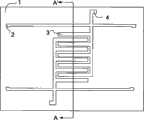
图1(a)为本发明的第一基板及其上的检测用交叉梳齿状固定对电极示意图;Fig. 1 (a) is the schematic diagram of the first substrate of the present invention and the interdigitated fixed counter electrode for detection thereon;
图1(b)为图1(a)中沿A-A’向的器件结构的分解断面图;Fig. 1 (b) is the exploded sectional view of the device structure along A-A ' in Fig. 1 (a);
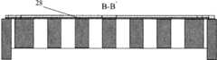
图2(a)为本发明的在第二基板上的结构示意图;Fig. 2 (a) is the structural representation on the second substrate of the present invention;
图2(b)为图2(a)中沿B-B’向的器件结构的分解断面图;Fig. 2 (b) is the exploded sectional view of the device structure along B-B ' among Fig. 2 (a);
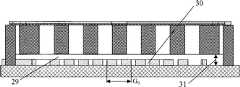
图3为图1(b)和图2(b)的断面图组合;Fig. 3 is the sectional view combination of Fig. 1 (b) and Fig. 2 (b);
图4为本发明的一对梳栅可动电极和梳齿固定电极的放大图;4 is an enlarged view of a pair of comb-grid movable electrodes and comb-teeth fixed electrodes of the present invention;
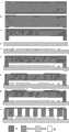
图5为本发明的制作工艺流程断面图。Fig. 5 is a sectional view of the manufacturing process flow of the present invention.
具体实施方式Detailed ways
以下结合实施例和附图对本发明进一步说明,但本发明决非仅限于所介绍的实施例。The present invention will be further described below in conjunction with the embodiments and accompanying drawings, but the present invention is by no means limited to the described embodiments.
本发明的实施例涉及一种电容式微惯性传感器,参考图1(a)、图1(b)、图2(a)、图2(b)、图3、图4和图5,在第一基板1上形成两组检测用交叉梳齿状固定对电极,对应固定质量块间的连接耦合电极2,以及连接耦合电极2与引出电极4之间的连接线,检测用交叉梳齿状固定对电极由沿横向相对交叉的梳齿电极3和引出电极组成;在第二基板上形成固定于第一基板1上的敏感器锚点12、第二基板的悬于第一基板1上方的可沿纵向运动的敏感器栅质量块25、将敏感器锚点12和敏感器栅质量块25相连的两根U形敏感器支撑梁8、敏感器可横向移动质量块27、将敏感器可横向移动质量块和敏感器栅质量块相连的U形敏感器连接梁17、固定质量块上的梳形固定电极、敏感器外部引出电极11、金属层下的电绝缘层28、电绝缘层上的驱动导线14和驱动导线引出电极,其中驱动导线引出电极包括驱动导线左侧引出电极10和驱动导线右侧引出电极13。如图2(a)、2(b)、图3和图4所示,形成对应梳形可动电极梳齿15和梳形固定电极梳齿6间的横向间距G1,第一基板1与敏感器栅质量块25之间的间隙31,如图3中的双箭头所示;形成敏感器栅质量块与第一基板上的检测用交叉梳齿状固定对电极之间的间隙29;梳齿电极对内的两个梳齿电极之间的间隙30,每个梳齿电极对内的间隙相同。对应的一个梳形可动电极和一个梳形固定电极组成一对梳齿电容对,形成相邻梳齿电容对的纵向间距,其值不小于三十微米。Embodiments of the present invention relate to a capacitive micro-inertial sensor, with reference to Fig. 1 (a), Fig. 1 (b), Fig. 2 (a), Fig. 2 (b), Fig. 3, Fig. 4 and Fig. 5, in the first Two sets of cross-comb-shaped fixed counter electrodes for detection are formed on the
结合图1(a)、图1(b)、图2(a)、图2(b)、图3和图4,对本发明的结构进行说明。The structure of the present invention will be described with reference to Fig. 1(a), Fig. 1(b), Fig. 2(a), Fig. 2(b), Fig. 3 and Fig. 4 .
参考图2(a)、2(b),敏感器栅质量块是由纵向等间距、横向平行的栅形电极26、连接栅形电极的边框24及敏感器栅质量块矩形凸起21组成,敏感器栅质量块矩形凸起有两个,分别位于敏感器栅质量块两侧,在敏感器栅质量块的横向中心线上。Referring to Fig. 2(a), 2(b), the sensor grid mass is composed of vertically equidistant grid electrodes 26, horizontally parallel grid electrodes 26, a frame 24 connecting the grid electrodes and a sensor grid mass rectangular protrusion 21, There are two rectangular projections of the sensor grid mass, which are respectively located on both sides of the sensor grid mass and on the transverse centerline of the sensor grid mass.
参考图2(a)、2(b),敏感器可横向移动质量块有两个,分别位于敏感器栅质量块的两侧,由矩形块23、梳形可动电极和敏感器可横向移动质量块矩形凸起22组成,敏感器可横向移动质量块的纵向长度和敏感器栅质量块的主体长度相同;敏感器可横向移动质量块矩形凸起有两个,其位置位于矩形块的内侧,即和敏感器栅质量块矩形凸起相对应的一侧,和敏感器栅质量块矩形凸起对应设置,形成电容调整间隙18。每个敏感器可横向移动质量块和敏感器栅质量块通过两根位于敏感器可横向移动质量块和敏感器栅质量块之间的U形敏感器连接梁17相连,该两根U形敏感器连接梁沿着敏感器栅质量块的横向中心线对称设置,该两根U形敏感器连接梁沿着敏感器栅质量块的纵向中心线与位于敏感器栅质量块另一侧的另两根U形敏感器连接梁对应对称设置,实现敏感器可横向移动质量块的横向敏感。每根敏感器连接梁始于矩形块的一角,终于敏感器栅质量块的边框24的对应角,敏感器连接梁的U形靠近敏感器栅质量块的横向中心线。Referring to Figure 2(a), 2(b), there are two laterally movable mass blocks of the sensor, which are respectively located on both sides of the mass block of the sensor grid, and are composed of a rectangular block 23, a comb-shaped movable electrode and a sensor that can move laterally The quality block is composed of rectangular protrusions 22, and the longitudinal length of the sensor’s laterally movable mass block is the same as the main body length of the sensor’s grid mass block; there are two rectangular protrusions of the sensor’s laterally movable mass block, which are located inside the rectangular block , that is, the side corresponding to the rectangular protrusion of the sensor grid mass is set corresponding to the rectangular protrusion of the sensor grid mass, forming a capacitance adjustment gap 18 . Each sensor movable mass and the sensor grid mass are connected by two U-shaped sensor connecting beams 17 between the sensor movable mass and the sensor grid mass. The sensor connecting beams are arranged symmetrically along the transverse centerline of the sensor grid mass, and the two U-shaped sensor connecting beams are connected to the other two on the other side of the sensor grid mass The connecting beam of the U-shaped sensor is correspondingly arranged symmetrically, so as to realize the lateral sensitivity of the laterally movable mass of the sensor. Each sensor connecting beam starts from a corner of the rectangular block and ends at a corresponding corner of the frame 24 of the sensor grid mass. The U shape of the sensor connecting beam is close to the transverse centerline of the sensor grid mass.
参考图2(a)、2(b),梳形可动电极由四个等间距的梳形可动电极梳齿15和连接梳齿的梳形可动电极矩形条16组成,梳形可动电极梳齿15与梳形可动电极矩形条16垂直设置;梳形可动电极在矩形块的外侧分别对应组成两组硅条组,每组硅条组分别对应设置在矩形块的相应处,每组硅条组包括平行设置的三条梳形可动电极,连接梳形可动电极梳齿的梳形可动电极矩形条与矩形块侧边垂直设置。Referring to Figure 2(a), 2(b), the comb-shaped movable electrode is composed of four equally spaced comb-shaped movable electrode comb teeth 15 and a comb-shaped movable electrode rectangular strip 16 connected to the comb teeth, the comb-shaped movable electrode The electrode comb teeth 15 and the comb-shaped movable electrode rectangular strips 16 are vertically arranged; the comb-shaped movable electrodes are respectively formed into two sets of silicon strip groups on the outside of the rectangular block, and each group of silicon strip groups is respectively arranged at the corresponding position of the rectangular block. Each group of silicon strips includes three comb-shaped movable electrodes arranged in parallel, and the comb-shaped movable electrode rectangular strips connected to the comb teeth of the comb-shaped movable electrodes are vertically arranged to the side of the rectangular block.
参考图2(a)、2(b),矩形块一侧每组的梳形可动电极沿敏感器栅质量块的横向中心线对称设置,边框两侧的四组硅条组,每组梳形可动电极沿敏感器栅质量块的纵向中心线对应对称设置。Referring to Figures 2(a) and 2(b), the comb-shaped movable electrodes of each group on one side of the rectangular block are arranged symmetrically along the transverse center line of the sensor grid mass, and the four groups of silicon strips on both sides of the frame, each group of combs The movable electrodes are symmetrically arranged along the longitudinal centerline of the grid mass of the sensor.
参考图2(a)、2(b),敏感器锚点12沿敏感器栅质量块的纵向中心线分别设置在敏感器栅质量块的两端,并通过两根敏感器支撑梁对应与敏感器栅质量块连接,敏感器外部引出电极11设置在一个敏感器锚点上。Referring to Fig. 2(a) and 2(b), the sensor anchor points 12 are respectively arranged at both ends of the sensor grid mass along the longitudinal centerline of the sensor grid mass, and correspond to the sensor grid mass through two sensor support beams. The mass block of the sensor grid is connected, and the external lead-out electrode 11 of the sensor is set on a sensor anchor point.
参考图2(a)、2(b),每个固定质量块包括固定质量块锚点5和梳形固定电极,固定质量块与每组硅条组一一对应设置,固定质量块的与硅条组对应的一侧设置有三条和梳形可动电极外形相同的梳形固定电极,梳形固定电极由梳形固定电极梳齿和梳形固定电极矩形条组成,梳形可动电极由梳形可动电极梳齿和梳形可动电极矩形条组成,梳形固定电极梳齿和梳形可动电极梳齿形成间隙19,梳形可动电极和梳形固定电极的位置对应设置,梳形固定电极梳齿与梳形可动电极梳齿对应交叉设置。With reference to Fig. 2 (a), 2 (b), each fixed mass comprises fixed mass anchor point 5 and comb-shaped fixed electrode, and fixed mass is arranged in one-to-one correspondence with each group of silicon bar groups, and the fixed mass is connected to the silicon strip group. There are three comb-shaped fixed electrodes with the same shape as the comb-shaped movable electrodes on the corresponding side of the bar group. The comb-shaped fixed electrodes are composed of comb-shaped fixed electrode comb teeth and comb-shaped fixed electrode rectangular strips. Comb-shaped movable electrode comb teeth and comb-shaped movable electrode rectangular strips, the comb-shaped fixed electrode comb teeth and the comb-shaped movable electrode comb teeth form a gap 19, the positions of the comb-shaped movable electrode and the comb-shaped fixed electrode are set correspondingly, and the comb-shaped movable electrode and the comb-shaped fixed electrode are arranged correspondingly. The comb-teeth of the fixed electrode and the comb-teeth of the comb-shaped movable electrode are correspondingly intersected.
参考图2(a)、图2(b)、图3,驱动导线14共有两根,分别纵向设置于相应的矩形块上,每根驱动导线的一端通过沿对应的敏感器连接梁、边框端和敏感器支撑梁上所铺设的金属导线与对应的驱动导线引出电极连接。在驱动导线、金属导线、驱动导线引出电极组成的金属层与矩形块对应部分之间设置有电绝缘层。With reference to Fig. 2 (a), Fig. 2 (b), Fig. 3, there are two driving wires 14, which are vertically arranged on corresponding rectangular blocks respectively, and one end of each driving wire is connected to the beam and frame end along the corresponding sensor. The metal wire laid on the support beam of the sensor is connected with the corresponding driving wire lead-out electrode. An electric insulating layer is arranged between the metal layer composed of the driving wire, the metal wire, the driving wire lead-out electrode and the corresponding part of the rectangular block.
参考图2(a)和图4,电容调整间隙比对应梳形可动电极梳齿和梳形固定电极梳齿间的横向间距G1小一微米以上,传感器电容的起始检测间距是电容调整间隙与横向间距G1之间的差值。Referring to Figure 2(a) and Figure 4, the capacitance adjustment gap is more than one micron smaller than the horizontal distanceG1 between the comb-shaped movable electrode comb and the comb-shaped fixed electrode comb, and the initial detection distance of the sensor capacitance is the capacitance adjustment The difference between the gap and the lateral spacingG1 .
参考图1(a)、图1(b),检测用交叉梳齿状固定对电极由沿横向相对交叉的梳齿电极3和引出电极4组成,交叉的梳齿电极对应组成梳齿电极对。Referring to Fig. 1(a) and Fig. 1(b), the cross-comb-shaped fixed counter electrode for detection is composed of comb-teeth electrodes 3 and lead-out
参考图(3),栅形电极位于对应的梳齿电极对内两个梳齿电极之间的间隙30的正上方Referring to Figure (3), the grid-shaped electrode is located directly above the
结合图1(a)、图1(b)、图2(a)、图2(b)、图3和图4,形成的敏感器栅质量块上栅形电极的厚度小于第二极板厚度;In conjunction with Fig. 1(a), Fig. 1(b), Fig. 2(a), Fig. 2(b), Fig. 3 and Fig. 4, the thickness of the grid-shaped electrode on the formed sensor grid mass is less than the thickness of the second plate ;
为了更明确的描述检测电容的各个间距,结合图3和图4进一步描述,梳齿电极对两侧之间的距离如图3中的横向双箭头所示,用G0表示,其值大于栅形电极的宽度;敏感器栅质量上的梳形可动电极梳齿15与固定质量块上的梳形固定电极梳齿之间的间隙用G1表示,如图4中的相应箭头所示,取值范围为十微米到五十微米;敏感器栅质量上的梳形可动电极梳齿与固定质量块上的梳形固定电极梳齿之间的叠加的纵向尺寸,如图4中的相应箭头所示,用G2表示,其值不小于一微米;每对梳齿电容对中的梳形可动电极梳齿与对应的梳形固定电极矩形条之间的间距,如图4中的相应箭头所示,用G3表示,其值不小于十微米。栅形电极的下表面和检测用交叉梳齿状固定对电极之间的间隙29大于四微米,不大于栅形电极的宽度;栅形电极的宽度大于间隙30。In order to describe the distances of the detection capacitors more clearly, it is further described in conjunction with Fig. 3 and Fig. 4. The distance between the two sides of the comb-tooth electrode pair is shown by the horizontal double arrows in Fig. 3, represented by G0 , and its value is greater than The width of the electrode; the gap between the comb-shaped movable electrode comb teeth 15 on the sensor grid mass and the comb-shaped fixed electrode comb teeth on the fixed mass is represented byG1 , as shown by the corresponding arrows in Figure 4, The value range is ten microns to fifty microns; the superimposed longitudinal dimension between the comb-shaped movable electrode comb teeth on the sensor grid mass and the comb-shaped fixed electrode comb teeth on the fixed mass block, as shown in Figure 4 As shown by the arrow, it is represented byG2 , and its value is not less than one micron; the distance between the comb-shaped movable electrode comb teeth in each comb-shaped capacitor pair and the corresponding comb-shaped fixed electrode rectangular strip, as shown in Figure 4 As shown by the corresponding arrow, it is represented byG3 , and its value is not less than ten microns. The gap 29 between the lower surface of the grid-shaped electrode and the interdigitated fixed counter electrode for detection is greater than four microns, not greater than the width of the grid-shaped electrode; the width of the grid-shaped electrode is greater than the
本实施例涉及的电容式微惯性传感器的制作方法,参考图5所示的工艺流程图断面图进行说明,结构断面图取自图1中A-A’和图2中B-B’,主要包括以下工艺步骤:The manufacturing method of the capacitive micro-inertial sensor involved in this embodiment is explained with reference to the sectional view of the process flow diagram shown in Fig. 5. The structural sectional view is taken from AA' in Fig. 1 and BB' in Fig. 2, mainly including The following process steps:
a选用低阻硅片作为第二基板,在低阻硅的表面形成氧化硅作为电绝缘层;a select a low-resistance silicon wafer as the second substrate, and form silicon oxide on the surface of the low-resistance silicon as an electrical insulating layer;
b结合掩膜板,用光刻胶做掩膜,利用氢氟酸去除在低阻硅下表面的部分氧化硅,露出要刻蚀的悬浮区;b Combined with the mask plate, use photoresist as a mask, and use hydrofluoric acid to remove part of the silicon oxide on the lower surface of the low-resistance silicon, exposing the suspension area to be etched;
c用碱性容易腐蚀悬浮区,玻璃衬底与敏感器栅质量块之间的间隙31,并用氢氟酸去除低阻硅下表面的氧化硅;c It is easy to corrode the suspension area, the
d选用玻璃衬底作为第一基板;d select a glass substrate as the first substrate;
e在玻璃上表面形成铝材料的检测用交叉梳齿状固定对电极,连接耦合电极,连接耦合电极与检测用交叉梳齿状固定对电极之间的多根连接线,从而形成间隙30;e form a cross-comb-shaped fixed counter electrode of aluminum material on the upper surface of the glass, connect the coupling electrode, and connect multiple connection lines between the coupling electrode and the detection cross-comb-shaped fixed counter electrode, thereby forming a
f把检测用交叉梳齿状固定对电极对应在低阻硅的悬浮区,采用温度380摄氏度,电压800V,阳极键合玻璃衬底和低阻硅,形成敏感器栅质量块与玻璃衬底上的检测用交叉梳齿状固定对电极之间的间隙29;f Correspond to the cross-comb-shaped fixed counter electrode for detection in the suspension area of low-resistance silicon, use a temperature of 380 degrees Celsius and a voltage of 800V to anodically bond the glass substrate and low-resistance silicon to form the sensor grid mass and the glass substrate. The detection uses the gap 29 between the interdigitated fixed electrodes;
g刻蚀低阻硅上表面的电绝缘层,形成U形敏感器支撑梁和U形敏感器连接梁上的和驱动导线、驱动导线左侧引出电极10、驱动导线右侧引出电极13及金属导线20相应部位下的电绝缘层28;g etch the electrical insulation layer on the upper surface of the low-resistance silicon to form the U-shaped sensor support beam and the U-shaped sensor connecting beam and the drive wire, the left side of the drive wire lead electrode 10, the drive wire right side lead electrode 13 and the metal
h在电绝缘层28上形成对应的驱动导线、驱动导线引出电极及其他金属导线。在低阻硅上形成敏感器外部引出电极11;h Form corresponding driving wires, driving wire lead-out electrodes and other metal wires on the electrical insulating
i形成悬于玻璃衬底上方敏感器栅质量块、将敏感器锚点12和敏感器栅质量块相连的两根U形敏感器支撑梁、敏感器可横向移动质量块、将敏感器可横向移动质量块和敏感器栅质量块相连的U形敏感器连接梁、固定质量块上的梳形固定电极、敏感器外部引出电极。形成对应梳形可动电极梳齿和梳形固定电极梳齿间的横向间距G1,形成固定于玻璃衬底1上的敏感器锚点12。i form two U-shaped sensor support beams that are suspended above the glass substrate above the sensor grid mass and connect the sensor anchor point 12 with the sensor grid mass, the sensor can move the mass block laterally, and the sensor can move laterally The U-shaped sensor connecting beam connected to the moving mass and the sensor grid mass, the comb-shaped fixed electrode on the fixed mass, and the external lead-out electrode of the sensor. A transverse distance G1 between the corresponding comb-shaped movable electrode comb teeth and the comb-shaped fixed electrode comb teeth is formed to form a sensor anchor point 12 fixed on the
由以上工艺步骤制作出本发明涉及的高精度微惯性传感器。结合图1至图5对传感器原理进行说明。The high-precision micro-inertial sensor involved in the present invention is produced by the above process steps. The principle of the sensor will be described with reference to FIG. 1 to FIG. 5 .
敏感器栅质量块矩形凸起21和敏感器可横向移动质量块矩形凸起22之间的电容调整间隙18用d1表示,梳形固定电极梳齿6和梳形可动电极梳齿15的间隙19用G1表示,且G1=(d1+x),(x为传感器静态初始电容间距,x≥1,单位:微米)。把位于敏感器栅质量块左侧的驱动导线,用外部金丝球焊技术,用金线把驱动导线左侧引出电极10分别连接到封装管壳引脚上,并接入恒流源。把位于敏感器栅质量块右侧的驱动导线,用外部金丝球焊技术,用金线把驱动导线右侧引出电极分别连接到封装管壳引脚上,并接入和左侧的驱动导线相反相位的恒流源。敏感器外部引出电极连接到封装管壳引脚,并连接到地,引出电极4分别连接到封装管壳引脚,并分别用V1和V2表示,在用微机械工艺加工传感器时,G1、d1可以设置较大值,加工出较厚的传感器质量块,因而质量块质量较大。在传感器结构正上方的封装管壳帽内设置合适方向的匀强磁场,使在两根金属驱动导线上产生的安培力的方向均指向敏感器栅质量块的纵向中心线,并与敏感器栅质量块的纵向中心线垂直。两根驱动导线上的安培力使敏感器栅质量块矩形凸起21和敏感器可横向移动质量块矩形凸起22之间的电容调整间隙18减小至零,此时,测试传感器静态初始电容间距为G1-d1,由于电容的间距大大减小,从而传感器的初始检测电容大大增加。再在V1、V2端分别加电载波信号,可动质量块通过锚点连接至地。当敏感方向上有加速度信号时,由于惯性力的作用,产生位移,从而引起敏感器栅质量块25上的栅形电极26和检测用交叉梳齿状固定对电极组成的差分电容的叠加面积变化以及对应梳形固定电极梳齿6和梳形可动电极梳齿15对应组成的差分电容的叠加面积变化,进而引起电容较大的变化,该变化电容和外部惯性信号的大小成线性关系,通过检测电容变化便可以得到敏感方向上加速度的大小,而且由于传感器结构设计的特点,检测电容为差分变化,这增大了传感器的线性范围和量程。The capacitance adjustment gap 18 between the rectangular protrusion 21 of the grid mass of the sensor and the rectangular protrusion 22 of the laterally movable mass of the sensor is represented by d1, and the gap between the comb-shaped fixed electrode comb teeth 6 and the comb-shaped movable electrode comb teeth 15 19 is represented by G1 , and G1 =(d1+x), (x is the static initial capacitance distance of the sensor, x≥1, unit: micron). Connect the driving wires located on the left side of the sensor grid mass to the external gold wire ball bonding technology, and use gold wires to connect the left electrode 10 of the driving wires to the pins of the package shell respectively, and connect to the constant current source. Connect the driving wires on the right side of the sensor grid mass to the external gold wire ball bonding technology, use gold wires to connect the electrodes on the right side of the driving wires to the pins of the package shell, and connect them to the driving wires on the left side Constant current sources of opposite phases. The external lead electrodes of the sensor are connected to the pins of the package shell and connected to the ground. The
本发明涉及的高精度微惯性传感器,由于梳齿电容间距可用安培力驱动驱动导线减小,从而在不增加横向尺寸的情况下增大了振子质量和检测电容,且检测电容极板间的相对运动主要表现为滑膜阻尼,这些因素使传感器的机械噪声和电路噪声大大减小,从而使传感器可以达到很高的精度,同时本发明采用微机械技术制作,工艺简单,有利于提高成品率和降低制造成本。The high-precision micro-inertial sensor involved in the present invention can increase the quality of the vibrator and the detection capacitance without increasing the lateral dimension because the comb-tooth capacitance spacing can be driven by the ampere force to reduce the relative distance between the plates of the detection capacitance. The movement is mainly manifested as synovial film damping. These factors greatly reduce the mechanical noise and circuit noise of the sensor, so that the sensor can achieve high precision. At the same time, the invention is made by micro-mechanical technology, and the process is simple, which is conducive to improving the yield and Reduce manufacturing costs.
Claims (2)
Priority Applications (1)
| Application Number | Priority Date | Filing Date | Title |
|---|---|---|---|
| CN201010125451XACN101792109B (en) | 2010-03-16 | 2010-03-16 | Micro inertial sensor with embedded transversely movable electrodes and manufacturing method thereof |
Applications Claiming Priority (1)
| Application Number | Priority Date | Filing Date | Title |
|---|---|---|---|
| CN201010125451XACN101792109B (en) | 2010-03-16 | 2010-03-16 | Micro inertial sensor with embedded transversely movable electrodes and manufacturing method thereof |
Publications (2)
| Publication Number | Publication Date |
|---|---|
| CN101792109Atrue CN101792109A (en) | 2010-08-04 |
| CN101792109B CN101792109B (en) | 2012-01-11 |
Family
ID=42585069
Family Applications (1)
| Application Number | Title | Priority Date | Filing Date |
|---|---|---|---|
| CN201010125451XAExpired - Fee RelatedCN101792109B (en) | 2010-03-16 | 2010-03-16 | Micro inertial sensor with embedded transversely movable electrodes and manufacturing method thereof |
Country Status (1)
| Country | Link |
|---|---|
| CN (1) | CN101792109B (en) |
Cited By (6)
| Publication number | Priority date | Publication date | Assignee | Title |
|---|---|---|---|---|
| CN103344785A (en)* | 2013-07-22 | 2013-10-09 | 杭州电子科技大学 | Capacitive micro inertial sensor with self calibration function |
| CN104155475A (en)* | 2014-08-04 | 2014-11-19 | 南京信息工程大学 | Capacitive micro mechanical accelerometer and manufacturing method thereof |
| CN104459200A (en)* | 2013-09-18 | 2015-03-25 | 上海矽睿科技有限公司 | Three-axis accelerometer |
| CN107782916A (en)* | 2016-08-27 | 2018-03-09 | 深迪半导体(上海)有限公司 | A kind of triaxial accelerometer |
| CN109444466A (en)* | 2017-08-30 | 2019-03-08 | 意法半导体股份有限公司 | FM inertial sensor and method for operating FM inertial sensor |
| CN110058052A (en)* | 2019-04-02 | 2019-07-26 | 杭州士兰微电子股份有限公司 | Inertial sensor and its manufacturing method |
Citations (5)
| Publication number | Priority date | Publication date | Assignee | Title |
|---|---|---|---|---|
| KR20040081915A (en)* | 2003-03-17 | 2004-09-23 | 삼성전자주식회사 | Microgyroscopes |
| US20050166675A1 (en)* | 2004-01-30 | 2005-08-04 | Hobbs Larry P. | Micromachined vibratory gyroscope and method with electronic coupling |
| CN101481084A (en)* | 2009-02-13 | 2009-07-15 | 杭州电子科技大学 | Micro-inertial sensor with variable pitch capacitor and method for producing the same |
| CN101531334A (en)* | 2009-04-07 | 2009-09-16 | 杭州电子科技大学 | Magnetic drive micro-inertial sensor for increasing detection capacitance and preparation method |
| CN201694830U (en)* | 2010-03-16 | 2011-01-05 | 杭州电子科技大学 | A Micro-Inertial Sensor Embedded with Transversely Movable Electrodes |
- 2010
- 2010-03-16CNCN201010125451XApatent/CN101792109B/ennot_activeExpired - Fee Related
Patent Citations (5)
| Publication number | Priority date | Publication date | Assignee | Title |
|---|---|---|---|---|
| KR20040081915A (en)* | 2003-03-17 | 2004-09-23 | 삼성전자주식회사 | Microgyroscopes |
| US20050166675A1 (en)* | 2004-01-30 | 2005-08-04 | Hobbs Larry P. | Micromachined vibratory gyroscope and method with electronic coupling |
| CN101481084A (en)* | 2009-02-13 | 2009-07-15 | 杭州电子科技大学 | Micro-inertial sensor with variable pitch capacitor and method for producing the same |
| CN101531334A (en)* | 2009-04-07 | 2009-09-16 | 杭州电子科技大学 | Magnetic drive micro-inertial sensor for increasing detection capacitance and preparation method |
| CN201694830U (en)* | 2010-03-16 | 2011-01-05 | 杭州电子科技大学 | A Micro-Inertial Sensor Embedded with Transversely Movable Electrodes |
Cited By (9)
| Publication number | Priority date | Publication date | Assignee | Title |
|---|---|---|---|---|
| CN103344785A (en)* | 2013-07-22 | 2013-10-09 | 杭州电子科技大学 | Capacitive micro inertial sensor with self calibration function |
| CN104459200A (en)* | 2013-09-18 | 2015-03-25 | 上海矽睿科技有限公司 | Three-axis accelerometer |
| CN104459200B (en)* | 2013-09-18 | 2018-03-06 | 上海矽睿科技有限公司 | Three axis accelerometer |
| CN104155475A (en)* | 2014-08-04 | 2014-11-19 | 南京信息工程大学 | Capacitive micro mechanical accelerometer and manufacturing method thereof |
| CN104155475B (en)* | 2014-08-04 | 2015-09-16 | 南京信息工程大学 | Capacitance type micromechanical accelerometer and manufacture method thereof |
| CN107782916A (en)* | 2016-08-27 | 2018-03-09 | 深迪半导体(上海)有限公司 | A kind of triaxial accelerometer |
| CN109444466A (en)* | 2017-08-30 | 2019-03-08 | 意法半导体股份有限公司 | FM inertial sensor and method for operating FM inertial sensor |
| US10809280B2 (en) | 2017-08-30 | 2020-10-20 | Stmicroelectronics S.R.L. | FM inertial sensor and method for operating the FM inertial sensor |
| CN110058052A (en)* | 2019-04-02 | 2019-07-26 | 杭州士兰微电子股份有限公司 | Inertial sensor and its manufacturing method |
Also Published As
| Publication number | Publication date |
|---|---|
| CN101792109B (en) | 2012-01-11 |
Similar Documents
| Publication | Publication Date | Title |
|---|---|---|
| CN101481084B (en) | Micro-inertial sensor with variable pitch capacitor | |
| CN100552453C (en) | Symmetric straight beam capacitive micro-acceleration sensor and manufacturing method thereof | |
| CN102798734B (en) | MEMS triaxial accelerometer and manufacture method thereof | |
| CN105137120B (en) | A kind of V-beam torsional pendulum type single shaft micro-mechanical accelerometer and preparation method thereof | |
| CN102128953B (en) | Capacitive micro-accelerometer with symmetrical tilted folded beam structure | |
| CN101792108B (en) | Large capacitance micro inertial sensor based on slide-film damping and manufacturing method thereof | |
| CN103344785A (en) | Capacitive micro inertial sensor with self calibration function | |
| CN102759637A (en) | MEMS (micro electro mechanical system) triaxial acceleration transducer and manufacture method thereof | |
| CN104698222A (en) | Tri-axial monolithic integration resonant capacitance type micro-accelerometer and machining method thereof | |
| CN101271124B (en) | L-shaped beam piezoresistive micro-accelerometer and manufacturing method thereof | |
| CN101173958A (en) | Two-way micro-inertial sensor and manufacturing method thereof | |
| CN101792109A (en) | Micro inertial sensor with transversely movable electrodes embedded and manufacturing method thereof | |
| CN1559882A (en) | A tuning fork micromechanical gyro and its manufacturing method | |
| CN100449265C (en) | A horizontal axis micromachined gyro and its preparation method | |
| CN109001490A (en) | High-sensitivity torsional pendulum type silicon micro-accelerometer and preparation method thereof | |
| CN101531334B (en) | Magnetic drive micro-inertial sensor for increasing detection capacitance and preparation method | |
| CN104198762A (en) | Eight-beam symmetrical silicon micro-accelerometer | |
| CN115407084B (en) | A comb-tooth capacitive accelerometer | |
| CN102101637B (en) | Micro inertial sensor with embedded transverse movable electrode | |
| CN201852851U (en) | Framed capacitive silicon micromachined accelerometers | |
| CN201628723U (en) | A large-capacitance micro-inertial sensor based on synovial film damping | |
| CN1291232C (en) | Minitype angular velocity sensor and its making method | |
| CN201694830U (en) | A Micro-Inertial Sensor Embedded with Transversely Movable Electrodes | |
| CN201673168U (en) | Low Stress Silicon Microresonant Accelerometer | |
| CN101525115A (en) | Micro inertial sensor embedded with movable electrode and manufacturing method thereof |
Legal Events
| Date | Code | Title | Description |
|---|---|---|---|
| C06 | Publication | ||
| PB01 | Publication | ||
| C10 | Entry into substantive examination | ||
| SE01 | Entry into force of request for substantive examination | ||
| C14 | Grant of patent or utility model | ||
| GR01 | Patent grant | ||
| CF01 | Termination of patent right due to non-payment of annual fee | Granted publication date:20120111 Termination date:20150316 | |
| EXPY | Termination of patent right or utility model |