CN101785081B - Substantially planar light-emitting and/or UV-emitting structures - Google Patents
Substantially planar light-emitting and/or UV-emitting structuresDownload PDFInfo
- Publication number
- CN101785081B CN101785081BCN200780053652XACN200780053652ACN101785081BCN 101785081 BCN101785081 BCN 101785081BCN 200780053652X ACN200780053652X ACN 200780053652XACN 200780053652 ACN200780053652 ACN 200780053652ACN 101785081 BCN101785081 BCN 101785081B
- Authority
- CN
- China
- Prior art keywords
- emitting
- light
- electrode
- interlayer dielectric
- less
- Prior art date
- Legal status (The legal status is an assumption and is not a legal conclusion. Google has not performed a legal analysis and makes no representation as to the accuracy of the status listed.)
- Expired - Fee Related
Links
Images


Classifications
- H—ELECTRICITY
- H01—ELECTRIC ELEMENTS
- H01J—ELECTRIC DISCHARGE TUBES OR DISCHARGE LAMPS
- H01J61/00—Gas-discharge or vapour-discharge lamps
- H01J61/02—Details
- H01J61/04—Electrodes; Screens; Shields
- H01J61/10—Shields, screens, or guides for influencing the discharge
- H—ELECTRICITY
- H01—ELECTRIC ELEMENTS
- H01J—ELECTRIC DISCHARGE TUBES OR DISCHARGE LAMPS
- H01J61/00—Gas-discharge or vapour-discharge lamps
- H01J61/02—Details
- H01J61/30—Vessels; Containers
- H01J61/305—Flat vessels or containers
- B—PERFORMING OPERATIONS; TRANSPORTING
- B32—LAYERED PRODUCTS
- B32B—LAYERED PRODUCTS, i.e. PRODUCTS BUILT-UP OF STRATA OF FLAT OR NON-FLAT, e.g. CELLULAR OR HONEYCOMB, FORM
- B32B17/00—Layered products essentially comprising sheet glass, or glass, slag, or like fibres
- B32B17/06—Layered products essentially comprising sheet glass, or glass, slag, or like fibres comprising glass as the main or only constituent of a layer, next to another layer of a specific material
- B32B17/10—Layered products essentially comprising sheet glass, or glass, slag, or like fibres comprising glass as the main or only constituent of a layer, next to another layer of a specific material of synthetic resin
- B32B17/10005—Layered products essentially comprising sheet glass, or glass, slag, or like fibres comprising glass as the main or only constituent of a layer, next to another layer of a specific material of synthetic resin laminated safety glass or glazing
- B32B17/1055—Layered products essentially comprising sheet glass, or glass, slag, or like fibres comprising glass as the main or only constituent of a layer, next to another layer of a specific material of synthetic resin laminated safety glass or glazing characterized by the resin layer, i.e. interlayer
- B32B17/10761—Layered products essentially comprising sheet glass, or glass, slag, or like fibres comprising glass as the main or only constituent of a layer, next to another layer of a specific material of synthetic resin laminated safety glass or glazing characterized by the resin layer, i.e. interlayer containing vinyl acetal
- B—PERFORMING OPERATIONS; TRANSPORTING
- B32—LAYERED PRODUCTS
- B32B—LAYERED PRODUCTS, i.e. PRODUCTS BUILT-UP OF STRATA OF FLAT OR NON-FLAT, e.g. CELLULAR OR HONEYCOMB, FORM
- B32B17/00—Layered products essentially comprising sheet glass, or glass, slag, or like fibres
- B32B17/06—Layered products essentially comprising sheet glass, or glass, slag, or like fibres comprising glass as the main or only constituent of a layer, next to another layer of a specific material
- B32B17/10—Layered products essentially comprising sheet glass, or glass, slag, or like fibres comprising glass as the main or only constituent of a layer, next to another layer of a specific material of synthetic resin
- B32B17/10005—Layered products essentially comprising sheet glass, or glass, slag, or like fibres comprising glass as the main or only constituent of a layer, next to another layer of a specific material of synthetic resin laminated safety glass or glazing
- B32B17/1055—Layered products essentially comprising sheet glass, or glass, slag, or like fibres comprising glass as the main or only constituent of a layer, next to another layer of a specific material of synthetic resin laminated safety glass or glazing characterized by the resin layer, i.e. interlayer
- B32B17/10788—Layered products essentially comprising sheet glass, or glass, slag, or like fibres comprising glass as the main or only constituent of a layer, next to another layer of a specific material of synthetic resin laminated safety glass or glazing characterized by the resin layer, i.e. interlayer containing ethylene vinylacetate
- H—ELECTRICITY
- H01—ELECTRIC ELEMENTS
- H01J—ELECTRIC DISCHARGE TUBES OR DISCHARGE LAMPS
- H01J61/00—Gas-discharge or vapour-discharge lamps
- H01J61/02—Details
- H01J61/04—Electrodes; Screens; Shields
- H—ELECTRICITY
- H01—ELECTRIC ELEMENTS
- H01J—ELECTRIC DISCHARGE TUBES OR DISCHARGE LAMPS
- H01J61/00—Gas-discharge or vapour-discharge lamps
- H01J61/02—Details
- H01J61/30—Vessels; Containers
- H01J61/35—Vessels; Containers provided with coatings on the walls thereof; Selection of materials for the coatings
- H—ELECTRICITY
- H01—ELECTRIC ELEMENTS
- H01J—ELECTRIC DISCHARGE TUBES OR DISCHARGE LAMPS
- H01J61/00—Gas-discharge or vapour-discharge lamps
- H01J61/02—Details
- H01J61/54—Igniting arrangements, e.g. promoting ionisation for starting
- H—ELECTRICITY
- H01—ELECTRIC ELEMENTS
- H01J—ELECTRIC DISCHARGE TUBES OR DISCHARGE LAMPS
- H01J61/00—Gas-discharge or vapour-discharge lamps
- H01J61/02—Details
- H01J61/54—Igniting arrangements, e.g. promoting ionisation for starting
- H01J61/547—Igniting arrangements, e.g. promoting ionisation for starting using an auxiliary electrode outside the vessel
- H—ELECTRICITY
- H01—ELECTRIC ELEMENTS
- H01J—ELECTRIC DISCHARGE TUBES OR DISCHARGE LAMPS
- H01J65/00—Lamps without any electrode inside the vessel; Lamps with at least one main electrode outside the vessel
- H—ELECTRICITY
- H01—ELECTRIC ELEMENTS
- H01J—ELECTRIC DISCHARGE TUBES OR DISCHARGE LAMPS
- H01J65/00—Lamps without any electrode inside the vessel; Lamps with at least one main electrode outside the vessel
- H01J65/04—Lamps in which a gas filling is excited to luminesce by an external electromagnetic field or by external corpuscular radiation, e.g. for indicating plasma display panels
- H01J65/042—Lamps in which a gas filling is excited to luminesce by an external electromagnetic field or by external corpuscular radiation, e.g. for indicating plasma display panels by an external electromagnetic field
- H01J65/046—Lamps in which a gas filling is excited to luminesce by an external electromagnetic field or by external corpuscular radiation, e.g. for indicating plasma display panels by an external electromagnetic field the field being produced by using capacitive means around the vessel
- H—ELECTRICITY
- H05—ELECTRIC TECHNIQUES NOT OTHERWISE PROVIDED FOR
- H05B—ELECTRIC HEATING; ELECTRIC LIGHT SOURCES NOT OTHERWISE PROVIDED FOR; CIRCUIT ARRANGEMENTS FOR ELECTRIC LIGHT SOURCES, IN GENERAL
- H05B41/00—Circuit arrangements or apparatus for igniting or operating discharge lamps
- H05B41/14—Circuit arrangements
- H05B41/24—Circuit arrangements in which the lamp is fed by high frequency AC, or with separate oscillator frequency
Landscapes
- Physics & Mathematics (AREA)
- Engineering & Computer Science (AREA)
- Plasma & Fusion (AREA)
- Electromagnetism (AREA)
- Joining Of Glass To Other Materials (AREA)
- Laminated Bodies (AREA)
- Vessels And Coating Films For Discharge Lamps (AREA)
- Luminescent Compositions (AREA)
- Illuminated Signs And Luminous Advertising (AREA)
Abstract
Translated fromChinese
Description
Translated fromChinese本发明涉及发光和/或发射UV的结构这一领域,更特别的是涉及基本为平面的发光和/或发射UV的结构,该结构具有第一和第二电介质壁,二者彼此相对并限定出一个内部空间,该内部空间中包含光和/或UV源,该结构还具有光或UV源的第一和第二电极,其生成电场线且所述电场线的至少一部分(one component)垂直于第一和第二电极,第一电极至少被提供或能够被提供以高频电磁信号。 The present invention relates to the field of light-emitting and/or UV-emitting structures, and more particularly to substantially planar light-emitting and/or UV-emitting structures having first and second dielectric walls facing each other and defining An inner space containing light and/or UV source, the structure also has first and second electrodes of light or UV source, which generate electric field lines and at least one component of said electric field lines is vertical As for the first and second electrodes, the first electrode is at least provided or can be provided with a high-frequency electromagnetic signal. the
已知的平面发光结构是平面灯(flat lamp),其可以用作装饰或建筑光源,或用于液晶屏的背光。这些平面灯典型的由两个玻璃片组成,二者结合在一起并且之间具有很小的间隙,这一间隙通常小于几毫米,平面灯是气密的,其中含有减压状态下的气体,在气体中放电产生辐射,所述的辐射通常是紫外区的,这种辐射会激发光致发光材料,从而使其发射出可见光。 Known flat light-emitting structures are flat lamps, which can be used as decorative or architectural light sources, or for backlighting liquid crystal screens. These planar lamps typically consist of two glass sheets bonded together with a small gap, usually less than a few millimeters, and the planar lamp is airtight, containing gas under reduced pressure, The discharge in the gas produces radiation, usually in the ultraviolet region, which excites the photoluminescent material so that it emits visible light. the
文献WO 2004/015739A2公开了一种平面放电灯,其包括: Document WO 2004/015739A2 discloses a flat discharge lamp comprising:
-两个玻璃片形式的壁,它们保持在一起,彼此平行,限定出充满气体的内部空间,且在玻璃片对着内部空间的面上,涂覆了可被等离子气体激发的光致发光材料; - two walls in the form of glass sheets, held together, parallel to each other, delimiting a gas-filled interior space, and on the side of the glass sheets facing the interior space, coated with a photoluminescent material excitable by a plasma gas ;
-两个电极,其形式为分别覆盖内部空间外部两壁的均匀涂层,这两个电极产生电场线,且电场线的至少一部分与电极垂直;和 - two electrodes in the form of a uniform coating covering respectively the two outer walls of the interior space, which generate electric field lines, at least part of which are perpendicular to the electrodes; and
-通过塑料夹层薄膜连接在壁上的两个玻璃片。 - Two glass sheets connected to the wall by a plastic interlayer film. the
为了给这种类型的平面灯供电,至少一个电极处于V0的交流电势,该电势典型的数量级为kV,并且还处于高频状态,典型的约为1-100kHz,并且例如功率为约100W。 To power a planar lamp of this type, at least one electrode is at an alternating potential ofV , typically of the order of kV, and also at a high frequency, typically of the order of 1-100 kHz, and for example of a power of about 100W.
对于该申请,已经发现层合玻璃/塑料薄膜组件的绝缘性能是无法令人满意的。特别是,还发现只要良导体、例如金属导体接近与高频供电电极相关联的层合玻璃,在先技术中的平面灯就会出现安全性问题。 For this application, it has been found that the insulating properties of laminated glass/plastic film assemblies are unsatisfactory. In particular, it has also been found that the flat lamps of the prior art present safety problems whenever a good conductor, such as a metal conductor, approaches the laminated glass associated with the high-frequency supply electrodes. the
因此,本发明的目的在于,提供一种平面或基本为平面的发光结构, 其具有高频电源且其电场具有垂直分量,该结构具有增强的安全性能,同时避免显著增加结构中的功率消耗。 It is therefore an object of the present invention to provide a planar or substantially planar light-emitting structure with a high-frequency power supply and whose electric field has a vertical component, which structure has enhanced safety properties while avoiding a significant increase in power consumption in the structure. the
为了实现这一目的,本发明提供了一种发光或发射UV(紫外线)的结构: To achieve this purpose, the present invention provides a structure that emits light or UV (ultraviolet light):
-具有第一和第二电介质壁,其具有平的彼此相对的主面(mainface),并限定出内部空间,在内部空间中含有光和/或UV源;和 - having first and second dielectric walls, which have flat main faces (mainfaces) opposite each other, and define an inner space containing light and/or UV sources in the inner space; and
-光源的第一和第二电极,其产生电场线,且所述电场线的至少一部分与第一和第二电极垂直,第一和第二电极分别与第一和第二壁相连,第一电极被提供以频率为f0的高频电磁信号。 - first and second electrodes of the light source, which generate electric field lines, and at least a part of said electric field lines are perpendicular to the first and second electrodes, the first and second electrodes are respectively connected to the first and second walls, the first The electrodes are supplied with a high-frequency electromagnetic signal of frequency f0 .
本发明的这种发光或发射UV的结构进一步包括作为第一电极外罩的电气安全系统,该电气安全系统包括被称为保护导体的电导体,所述保护导体通过称为层间电介质的电介质与第一电极隔开,所述层间电介质基本是平面的且具有给定的电容C,所述保护导体连接到电源上,所述电源的电势V和/或频率f被调节,使得当f为0时外部泄漏电流的峰值等于2mA或更小,当f不为0时外部泄漏电流的峰值等于0.7mA或更小, This light-emitting or UV-emitting structure of the invention further comprises, as the first electrode housing, an electrical safety system comprising an electrical conductor called a protective conductor connected to The first electrode is separated, the interlayer dielectric is substantially planar and has a given capacitance C, the guard conductor is connected to a power supply whose potential V and/or frequency f is adjusted such that when f is When 0, the peak value of the external leakage current is equal to 2mA or less, when f is not 0, the peak value of the external leakage current is equal to 0.7mA or less,
层间电介质和/或保护导体和/或一个电极,按照这样的方式进行选择:使得至少在结构的表面温度选择为25℃-60℃之间时,层间电介质端部的消耗功率Pd等于或小于电源输出功率P的0.35倍。 The interlayer dielectric and/or the protective conductor and/or an electrode are selected in such a way that at least when the surface temperature of the structure is selected between 25°C and 60°C, the power dissipationPd at the end of the interlayer dielectric is equal to Or less than 0.35 times the output power P of the power supply.
Pd由下列等式得出:Pd=2πf0CU2sinδ,其中δ是层间电介质的损耗角,U是层间电介质端部之间的电压。 Pd is given by the following equation: Pd = 2πf0 CU2 sin δ, where δ is the loss angle of the interlayer dielectric and U is the voltage between the ends of the interlayer dielectric.
在现有技术的结构中,泄漏电流很高,因为其与以下因素成比例:(第一电极有效面积/金属体有效面积)比率、高频、高电势和灯的功率消耗。 In prior art structures the leakage current is high as it is proportional to the (first electrode active area/metal body active area) ratio, high frequency, high potential and power consumption of the lamp. the
在本发明的结构中,通过调节电导体的频率f和/或电势V,来限制泄漏电流,从而使得发光或发射UV的结构更为安全。 In the structure of the present invention, the leakage current is limited by adjusting the frequency f and/or the potential V of the electric conductor, thereby making the light-emitting or UV-emitting structure safer. the
向本发明的电导体提供的电势V和频率f或者它们的乘积V.f越低,则面积比就越高,且通常灯的尺寸越大。 The lower the potential V and the frequency f, or their product V.f, supplied to the electrical conductors of the invention, the higher the area ratio and generally the larger the size of the lamp. the
为了测量泄漏电流,优选使用面积与第一电极面积相等(最极端条件)的金属体。对于面积小于电极面积的金属体,电流按比例减小。 For measuring the leakage current, it is preferable to use a metal body having an area equal to that of the first electrode (the most extreme condition). For metal bodies with an area smaller than the electrode area, the current is proportionally reduced. the
如果V是交流电压,那么功率的数量级可以优选为100W,或者如果 V是直流电压或零电压,那么功率的数量级甚至可以达到1kW。 If V is an AC voltage, then the power may preferably be of the order of 100W, or even of the order of 1 kW if V is a DC voltage or zero voltage. the
该结构的面积尺寸可以相当于0.1m2或更大。 The areal size of the structure may be equivalent to 0.1m2 or larger.
第一电极和保护电导体之间的电介质,是具有电容性的夹层,其引入了电容C,在放电前该电容C与灯的给定电容C’并联,而电容C’由两电极之间的电介质(气体、电介质壁,等等)来决定。该夹层会影响灯的电供应,从而影响灯的性能。特别的,其能量消耗还会随着灯的温度改变。因此,必须限制Pd,优选通过减小乘积Csinδ来实现。 The dielectric between the first electrode and the protective electrical conductor is a capacitive interlayer which introduces a capacitance C which, before discharge, is in parallel with the given capacitance C' of the lamp, which is obtained between the two electrodes The dielectric (gas, dielectric wall, etc.) is determined. This interlayer affects the electrical supply to the lamp and thus the performance of the lamp. In particular, its power consumption also varies with the temperature of the lamp. Therefore,Pd must be limited, preferably by reducing the product Csinδ.
优选的,对于所述的表面温度,或者甚至是30℃-60℃之间的表面温度范围,甚至更优选的20℃-80℃,或甚至是-10℃-100℃(极限操作条件),Pd可以等于或小于0.25P,或者甚至是等于或小于0.15P。 Preferably, for said surface temperature, or even a surface temperature range between 30°C-60°C, even more preferably 20°C-80°C, or even -10°C-100°C (limit operating conditions),Pd may be equal to or less than 0.25P, or even equal to or less than 0.15P.
由于电容性夹层由其损耗角δ决定,并且其引入的电容C与相对电容率εr成比例,因此为了限制乘积Csinδ,夹层电介质可以选用具有合适电性能的材料,也就是说,其具有低tanδ值和/或低相对电容率εr,优选上述两个系数中的至少一个相对于温度保持恒定。 Since the capacitive interlayer is determined by its loss angle δ, and the capacitance C introduced by it is proportional to the relative permittivityεr , in order to limit the product Csinδ, the interlayer dielectric can be selected with suitable electrical properties, that is, it has a low The tan δ value and/or the low relative permittivity εr , preferably at least one of the above two coefficients is kept constant with respect to temperature.
为了实现这一目的,较为有利的是选择: To achieve this, it is advantageous to choose:
-在功率f0为1-100kHz,且所述表面温度下,或者甚至在30-60℃之间的温度范围下,甚至更优选在20℃-80℃之间,或者甚至是0℃-100℃之间的温度下,tanδ等于或小于0.06,或者甚至是等于或小于0.03;和/或 - at a powerf0 of 1-100 kHz and said surface temperature, or even in a temperature range between 30-60°C, even more preferably between 20°C-80°C, or even 0°C-100°C tan delta equal to or less than 0.06, or even equal to or less than 0.03 at temperatures between °C; and/or
-在功率f0为1-100kHz,且所述表面温度下,或者甚至在30-60℃之间的温度范围下,甚至更优选在20℃-80℃之间,或者甚至是0℃-100℃之间的温度下,相对电容率εr等于或小于4.5,或者甚至是等于或小于4,或甚至是等于或小于3.5。 - at a powerf0 of 1-100 kHz and said surface temperature, or even in a temperature range between 30-60°C, even more preferably between 20°C-80°C, or even 0°C-100°C The relative permittivity εr is equal to or less than 4.5, or even equal to or less than 4, or even equal to or less than 3.5 at a temperature between °C.
这是因为,当结构的温度升高时,由于损耗角δ增大,功率Pd也会随之升高。因此,使用这样的层间电介质是有利的:其电学性能随温度、特别是30℃-80℃之间的温度而变化很小。 This is because, when the temperature of the structure increases, the powerPd will also increase due to the increase of the loss angle δ. Therefore, it is advantageous to use an interlayer dielectric whose electrical properties vary little with temperature, especially at temperatures between 30°C and 80°C.
为了减小电容C,还可以不进行上述电学参数选择,仅进行实行下述措施;但是优选既进行上述电学参数选择,又实行下述措施,所述的措施包括: In order to reduce the electric capacity C, can also not carry out above-mentioned electrical parameter selection, only carry out following measure; But preferably both carry out above-mentioned electrical parameter selection, implement following measure again, described measure comprises:
-减小保护电导体和/或一个或两个电极的面积,优选通过以下方式实现:选用网格、或互相平行的导线、或平行或组成网格的导轨、或任何其 它的导电网络,和/或减小层间电介质的面积、或特别是正对保护电导体、电极和层间电介质的面积;和/或 - reducing the area of the protective electrical conductor and/or one or both electrodes, preferably by selecting a grid, or wires parallel to each other, or rails parallel or forming a grid, or any other conductive network, and/or reduce the area of the interlayer dielectric, or in particular the area facing the protective electrical conductors, electrodes and interlayer dielectric; and/or
-任选的增加层间电介质的厚度。 - Optionally increase the thickness of the interlayer dielectric. the
电介质还可以具有其它有利的性能: Dielectrics can also have other beneficial properties:
-满意的热机性能(可层压、良好的耐热性,等等); - Satisfactory thermomechanical properties (laminateable, good heat resistance, etc.);
-满意的光学性能(透明性,等等); - satisfactory optical properties (transparency, etc.);
-低密度(以限制结构的总重量);和 - low density (to limit the overall weight of the structure); and
-合理的成本。 - Reasonable cost. the
优选的,电介质包括或仅包括以下元件之一: Preferably, the dielectric includes or only includes one of the following elements:
-玻璃元件,例如玻璃片,其可以是两壁之一并可以选自: - a glass element, such as a glass sheet, which may be one of the two walls and may be selected from:
·厚的钠钙硅玻璃,其在全部区域构造上的最小厚度约为7mm; Thick soda-lime-silica glass with a minimum thickness of approximately 7 mm in all areas of construction;
·FeIII或Fe2O3含量至少为0.05%的钠钙硅玻璃,例如在全部区域构造中其最小厚度为6mm, Soda lime silica glass with a FeIII or Fe2 O3 content of at least 0.05%, for example a minimum thickness of 6 mm in all domain configurations,
·硼硅玻璃,例如在全部区域构造中其最小厚度为5mm,和 borosilicate glass, e.g. with a minimum thickness of 5 mm in all areas of construction, and
·二氧化硅或石英,例如在全部区域构造中其最小厚度为3mm; SiO2 or quartz, e.g. a minimum thickness of 3 mm in all domain structures;
-聚合物材料薄膜,例如: - Films of polymeric materials such as:
·聚对苯二甲酸乙二醇酯(PET)、聚乙烯醇缩丁醛(PVB)、聚氨酯(PU)、聚乙烯(PE)、聚萘二甲酸乙二醇酯(PEN)、聚氯乙烯(PVC)、或丙烯酸酯例如聚甲基丙烯酸甲酯(PMMA),这些材料在全部区域构造中(即基本上覆盖所连接的整个表面,例如该面的至少80%)的最小厚度为5mm,或者最特别的是 · Polyethylene terephthalate (PET), polyvinyl butyral (PVB), polyurethane (PU), polyethylene (PE), polyethylene naphthalate (PEN), polyvinyl chloride (PVC), or acrylates such as polymethyl methacrylate (PMMA), these materials have a minimum thickness of 5 mm in all area configurations (i.e. covering substantially the entire surface to be joined, for example at least 80% of the face), or most especially
·乙烯/醋酸乙烯酯(EVA)共聚物,在全部区域构造中其最小厚度为3mm,或者是聚碳酸酯(PC),在全部区域构造中其最小厚度例如为2mm;和 ethylene/vinyl acetate (EVA) copolymer with a minimum thickness of 3 mm in all areas of construction, or polycarbonate (PC) with a minimum thickness of, for example, 2 mm in all areas of construction; and
-气体,例如最小厚度为1mm的空气;或者最小厚度为2mm的惰性气体,例如氩气或氙气,其优选处于高压下从而使其难于离子化,所述惰性气体还例如是氮气。 - A gas such as air with a minimum thickness of 1 mm; or an inert gas such as argon or xenon with a minimum thickness of 2 mm, preferably at high pressure to make it difficult to ionize, also eg nitrogen. the
层间电介质可以是复合物电介质。其可以包括或仅包括上述几种元件,优选其厚度小于上述任意最小厚度,最特别的是: The interlayer dielectric may be a composite dielectric. It may comprise or consist only of several of the above elements, preferably having a thickness less than any of the above minimum thicknesses, most particularly:
-至少两种所述的聚合物薄膜,尤其是EVA薄膜和PC薄膜; - at least two of said polymer films, especially EVA films and PC films;
-气体和至少一种聚合物薄膜,尤其是EVA薄膜和/或PC薄膜; - gas and at least one polymer film, especially EVA film and/or PC film;
-气体和所述玻璃片,优选是较薄的玻璃片,例如当其是钠钙硅玻璃时,应使其厚度小于或等于4mm或3mm。 - the gas and said glass sheet, preferably a relatively thin glass sheet, eg when it is soda lime silica glass, should have a thickness less than or equal to 4 mm or 3 mm. the
还可以将层间电介质制成带有孔的(例如通孔)形式或甚至是不连续的形式,特别优选若干平行、等距且均匀分布的带,或者若干其它形状的段。层间电介质可以是上述玻璃片之一和/或一种或多种上述聚合物(PVB、PU、PET、EVA、PEN、PVC、PC、PMMA、等等)膜,且所述聚合物膜的厚度优选小于上述任意最小厚度。 It is also possible to make the interlayer dielectric in the form of holes (eg vias) or even in discontinuous form, particularly preferably several parallel, equidistant and uniformly distributed strips, or several other shaped segments. The interlayer dielectric may be one of the above-mentioned glass sheets and/or one or more of the above-mentioned polymer (PVB, PU, PET, EVA, PEN, PVC, PC, PMMA, etc.) films, and the polymer film The thickness is preferably less than any minimum thickness mentioned above. the
本发明适用于任何发光和/或发射UV的结构,且所述结构被提供以高频和电场E,所述电场E具有垂直分量(至少两个非共平面电极),本发明优选用于任意类型的放电型光源,也就是说,利用等离子气体发射光和/或紫外线的光源,或者当被等离子气体激发时,利用荧光体发射可见光。 The invention is applicable to any light-emitting and/or UV-emitting structure provided with a high frequency and an electric field E with a vertical component (at least two non-coplanar electrodes), the invention is preferably used in any type of discharge-type light source, that is, a light source that utilizes a plasma gas to emit light and/or ultraviolet light, or, when excited by a plasma gas, utilizes a phosphor to emit visible light. the
该结构可以是单向的和/或双向的照明(UV)灯、装饰灯、或显示器背光灯(液晶、电视、监视器,等等)。 The structures can be unidirectional and/or bidirectional lighting (UV) lights, decorative lights, or display backlights (LCD, TV, monitor, etc.). the
单向照明灯可以用于例如照明瓷砖(illuminating tiles)或用于LCD显示屏背光。 Unidirectional lights can be used, for example, for illuminating tiles or for backlighting LCD displays. the
此外,发射可见光的照明结构形成双层玻璃窗的主要部分,来取代窗户上的一个玻璃平面,或者与双层玻璃窗相连,例如合并到玻璃窗上。 Furthermore, the lighting structure emitting visible light forms an integral part of the double glazing, replacing a plane of glass on the window, or is connected to the double glazing, for example incorporated into the glazing. the
当然,对于双向照明,在结构中向外发射光线比光源还多的元件都是覆盖着普通部分且对于可见光和/或UV辐射基本或完全透明的(其形式例如为具有一定排列的吸收或反射图形,所述图形的分布满足:使得充分量的光和/或UV穿过它们)。 Of course, with bi-directional lighting, elements in the structure that emit more light outward than the light source are covered with common parts and are substantially or completely transparent (for example in the form of absorbing or reflecting graphics, the distribution of which is such that a sufficient amount of light and/or UV passes through them). the
在可见光区域,本发明的目的是,例如生产一种发光建筑物或装饰元件和/或具有显示功能的元件(发光显示元件、标识或标记),例如尤其是平面灯具,尤其是悬浮照明壁、照明瓷砖、等等。 In the visible region, the object of the invention is, for example, to produce a luminous architectural or decorative element and/or an element with a display function (luminous display element, sign or sign), such as in particular flat luminaires, in particular suspended lighting walls, Lighting tiles, etc. the
所选择的发光结构可以作为:建筑物或移动设施的发光窗户,如火车或轮船或飞机的窗子;屋顶;工业运输车辆的侧窗、后窗或挡风玻璃;玻璃窗;两间屋子或陆地、航空、航海工具中两块区域之间的内部隔段;陈列窗或橱窗;都市家具;建筑物表面。 The selected luminous structure can be used as: luminous windows of buildings or mobile installations, such as windows of trains or ships or airplanes; roofs; side windows, rear windows or windshields of industrial transport vehicles; glass windows; two houses or land Interior partitions between two areas in aviation and marine tools; display windows or showcases; urban furniture; building surfaces. the
能够传送UV辐射的电介质(形成一个或多个壁和/或层间绝缘部分和 /或覆盖绝缘部分的材料)优选可以选自:石英、二氧化硅、氟化镁(MgF2)或氟化钙(CaF2)、硼硅玻璃或Fe2O3含量少于0.05%的玻璃。 The dielectric (material forming one or more walls and/or interlayer insulation and/or covering insulation) capable of transmitting UV radiation may preferably be selected from: quartz, silicon dioxide, magnesium fluoride (MgF2 ) or fluorinated Calcium (CaF2 ), borosilicate glass or glass with Fe2 O3 content less than 0.05%.
以厚度为3mm的材料为例: Take a material with a thickness of 3mm as an example:
-氟化镁或氟化钙能够透射整个UV带中多于80%或甚至是90%的射线,也就是说UVA(315-380nm)、UVB(约280-315nm)、UVC(200-280nm)和VUV(约10-200nm); - Magnesium fluoride or calcium fluoride can transmit more than 80% or even 90% of the rays in the entire UV band, that is to say UVA (315-380nm), UVB (about 280-315nm), UVC (200-280nm) and VUV (about 10-200nm);
-石英和高纯度的二氧化硅能够透射整个UVA、UVB和UVC带中多于80%或甚至是90%的射线; -Quartz and high-purity silica can transmit more than 80% or even 90% of the rays in the entire UVA, UVB and UVC bands;
-硼硅玻璃、例如来自Schott的 能够透射整个UVA带中多于70%的射线;以及 - borosilicate glass, for example from Schott Able to transmit more than 70% of the total UVA band rays; and
-FeIII或Fe2O3含量小于0.05%的钠钙硅玻璃,尤其是来自Saint-Gobain的玻璃 

但是,钠钙硅玻璃、例如Saint-Gobain出售的玻璃 
在本发明的平面灯结构中,内部空间的气压可以在0.05-1巴左右。其中使用气体或气体混合物,例如:能够有效的发射所述UV射线的气体,尤其是氙、或汞或卤化物;或者是很容易电离形成等离子体(等离子气体)的气体,例如稀有气体如氖、氙、或氩、或氦,或卤素,或甚至是空气或氮气。 In the planar lamp structure of the present invention, the air pressure in the inner space can be around 0.05-1 bar. Wherein a gas or gas mixture is used, for example: a gas capable of effectively emitting said UV rays, especially xenon, or mercury or a halide; or a gas which is easily ionized to form a plasma (plasma gas), such as a rare gas such as neon , xenon, or argon, or helium, or halogens, or even air or nitrogen. the
(当将卤素与一种或多种稀有气体混合时),卤素的含量选为少于10%,例如4%。还可以使用卤代化合物。稀有气体和卤素的优点在于:对于环境条件不敏感。 (When the halogen is mixed with one or more noble gases), the halogen content is chosen to be less than 10%, for example 4%. Halogenated compounds can also be used. The advantage of noble gases and halogens is that they are not sensitive to ambient conditions. the
下表1示出了特别有效的UV-发射气体的辐射峰。 Table 1 below shows the radiation peaks of particularly effective UV-emitting gases. the
表1Table 1
上文所述的UV灯既可以用于工业领域,例如用于美容、生物医学、电子或食品领域,也可以用于家用领域,例如用于净化空气或自来水、饮用水或游泳池水,用于UV干燥或UV固化。 The UV lamps described above can be used both in industrial fields, such as in the cosmetic, biomedical, electronic or food fields, and in domestic fields, such as for purifying air or tap water, drinking water or swimming pool water, for UV drying or UV curing. the
通过选择UVA或甚至是UVB辐射,上述UV灯可以用于: By selecting UVA or even UVB radiation, the above UV lamps can be used for:
-美黑灯(根据标准,其尤其是在UVA带99.3%和UVB带0.7%); - Self-tanning lamps (according to the standard, it is especially in the UVA band 99.3% and UVB band 0.7%);
-皮肤病处理(尤其是在308nm的UVA辐照); - dermatological treatment (especially UVA irradiation at 308nm);
-光化活化方法,例如用于固化,尤其是粘合剂固化,或者用于交联,或用于纸张干燥; - actinic activation methods, e.g. for curing, especially adhesive curing, or for crosslinking, or for paper drying;
-荧光材料活化,例如活化凝胶状态的菲啶溴红,用以分析核酸或蛋白质;和 - activation of fluorescent materials, such as phenanthridine bromide red in gel state, for the analysis of nucleic acids or proteins; and
-激活光催化材料,例如用于减少冰箱臭味或污物。 -Activation of photocatalytic materials, eg for reduction of refrigerator odor or dirt. the
通过选择UVB辐射,这种灯可以促进皮肤中维生素D的形成。 By selecting UVB radiation, this lamp promotes the formation of vitamin D in the skin. the
通过选择UVC辐射,上述UV灯可以通过杀菌效应、尤其是250nm-260nm的杀菌效应,来消毒空气、水或表面。 By selecting the UVC radiation, the aforementioned UV lamps can disinfect air, water or surfaces through a germicidal effect, especially at 250nm-260nm. the
通过选择远UVC辐射或优选通过选择产生臭氧的VUV辐射,上述UV灯尤其是可以用于处理表面,特别是在沉积电子、计算机、光学物品、半导体等等的活性膜之前,可以用这种UV灯进行表面处理。 By selecting far UVC radiation or preferably by selecting ozone-generating VUV radiation, the aforementioned UV lamps can be used in particular for the treatment of surfaces, especially before the deposition of active films for electronics, computers, optical objects, semiconductors, etc. Lamps undergo surface treatment. the
例如,可以将UV灯与家用电子设备如冰箱、或橱柜进行组合。 For example, UV lamps can be combined with household electronics such as refrigerators, or cabinets. the
UV灯可以的尺寸可以与最近使用的荧光灯管类似,或者甚至比它更大,例如横截面积至少为0.1m2或甚至是1m2。 The UV lamps may be of similar size to, or even larger than, recently used fluorescent tubes, for example having a cross-sectional area of at least 0.1 m2 or even 1 m2 .
优选的,本发明的灯在所述可见光或UV辐射峰附近的透射系数为50%或更大,甚至优选是70%或更大,且甚至可以是80%或更大。 Preferably, the lamp according to the invention has a transmission coefficient around said visible or UV radiation peak of 50% or greater, even preferably 70% or greater, and may even be 80% or greater. the
在透射元件只有一面能够透射UV的UV灯结构中,另一壁可以是不透光的,例如玻璃-陶瓷或甚至是非玻璃电介质制成的,优选其具有相似的膨胀系数。 In UV lamp constructions where only one side of the transmissive element is UV-transmissive, the other wall can be opaque, for example made of glass-ceramic or even a non-glass dielectric, preferably with a similar coefficient of expansion. the
该结构中可以包括能够反射UV或可见光辐射的材料,该材料部分或全部覆盖一个壁的内表面或外主面,所述材料例如铝或氧化铝。电极之一可以由所述的反射材料制成。这种材料还为结构中存在的聚合物材料提供UV防护,从而避免其老化或变黄。 The structure may include a material capable of reflecting UV or visible radiation, covering partially or completely the inner or outer main surface of one wall, such as aluminum or aluminum oxide. One of the electrodes can be made of said reflective material. This material also provides UV protection to the polymeric material present in the structure, preventing it from aging or yellowing. the
当电极位于内表面时,层间电介质可以包括或作为一个壁。 When the electrodes are on the inner surface, the interlayer dielectric may comprise or act as a wall. the
作为替代方案,第一和第二电极可以至少部分的位于第一和第二壁中或位于其外主面上,这对于由市售钠钙硅玻璃形成壁的结构是特别适用的,这样的话,对于层间电介质就会保留更宽范围的选择。 Alternatively, the first and second electrodes may be located at least partially in the first and second walls or on their outer main faces, which is particularly suitable for structures in which the walls are formed from commercially available soda-lime-silica glass, in which case , a wider range of options remains for the interlayer dielectric. the
当组装该结构时,第一电极优选设置在较为不易接近的一侧,例如当该结构作为瓷砖时,将第一电极设置在地面一侧。 When assembling the structure, the first electrode is preferably arranged on a side that is less accessible, for example, when the structure is used as a tile, the first electrode is arranged on the ground side. the
保护电导体可以是连续的层,或者特别是为了减少C,保护电导体可以是非连续层(例如带的形式)或其可以是网格或导线。 The protective electrical conductor may be a continuous layer, or in particular for C reduction the protective electrical conductor may be a discontinuous layer (for example in the form of a tape) or it may be a mesh or a wire. the
在一种实施方式中,电势B是地电位。 In one embodiment, potential B is ground potential. the
因此,保护电导体作为屏蔽,使该结构是完全孤立的,从而使得泄漏电流为0。 Therefore, the protective electrical conductor acts as a shield so that the structure is completely isolated so that the leakage current is zero. the
优选的,第二电极可以接地,更优选的,保护电导体和第二电极任选的与灯或UV光源供电回路中的同一点相接。 Preferably, the second electrode can be grounded. More preferably, the protective electrical conductor and the second electrode are optionally connected to the same point in the power supply circuit of the lamp or UV light source. the
在后一种实施方式中,保护电导体是例如沉积在层间电介质(如果是内部电极,则任选的处于一个壁上)上的一层,以得到最佳的紧密性和生产简单性。可以利用层合的玻璃罩和/或薄膜对该层进行保护,使之免于刮伤,也可以保护导体使之不会脱落。 In the latter embodiment, the protective electrical conductor is eg a layer deposited on the interlayer dielectric (and optionally on one of the walls in the case of internal electrodes) for optimum compactness and production simplicity. This layer can be protected from scratching by a laminated cover glass and/or film, and the conductors can also be protected from detachment. the
如果是电极处于外部,保护电导体还可以是沉积在额外的外部绝缘基体内或外主面上的层,所述的额外的外部绝缘基体例如层合的玻璃外罩,这样可以得到更大的强度。 If the electrodes are external, the protective electrical conductor can also be a layer deposited in or on the outer main surface of an additional external insulating matrix, such as a laminated glass envelope, which results in greater strength . the
如果电极在内主面上,那么就形成了包括网格形式的保护电导体的增强玻璃。这样的结构保留了紧密性和强度。 If the electrodes are on the inner main face, then a reinforced glass is formed comprising a protective electrical conductor in the form of a grid. Such a structure retains compactness and strength. the
作为一种变型,电势V也可以是直流的,例如等于12V、24V或48V,特别是如果使用上述的玻璃型绝缘体,那么对于直流电势的值是无限制的。 As a variant, the potential V can also be DC, for example equal to 12V, 24V or 48V, especially if the aforementioned glass-type insulator is used, then there is no limit to the value of the DC potential. the
在一种实施方式中,将电极设置在外主面上,且保护电气系统包括其它的覆盖电介质(除空气外),该电介质位于保护电导体的上面,并且电势V为400V或更小,优选为220V或更小,还更优选110V或更小,和/或f为100Hz或更小,优选为60Hz或更小,还更优选50Hz或更小。 In one embodiment the electrodes are arranged on the outer main face and the protective electrical system comprises a further covering dielectric (other than air) which is located above the protective electrical conductor and which has a potential V of 400 V or less, preferably 220 V or less, still more preferably 110 V or less, and/or f is 100 Hz or less, preferably 60 Hz or less, still more preferably 50 Hz or less. the
此外,第二电极的电势和频率基本与上述相同,以使该结构更加便利。 In addition, the potential and frequency of the second electrode are substantially the same as above to make the structure more convenient. the
电势V优选为220V或更小,且频率f优选为50Hz或更小。 The potential V is preferably 220 V or less, and the frequency f is preferably 50 Hz or less. the
该覆盖电介质可以包括玻璃片,且玻璃片的厚度优选为4mm或更小,以避免厚度过大和/或超重带来的成本增加。 The covering dielectric may include a glass sheet, and the thickness of the glass sheet is preferably 4mm or less, so as to avoid cost increase caused by excessive thickness and/or weight. the
当然,覆盖电介质的厚度越小,电势V和/或频率f就会得到越多的限制。 Of course, the smaller the thickness of the covering dielectric, the more confinement the potential V and/or the frequency f will be. the
由于第二电极还可以被提供或能够被提供以高频电磁信号,所以该发光结构可以优选包括其它的电气安全系统,例如与上文所述类似的安全系统。在这种结构中,层间电介质是双重的,也就是说其由两部分组成,每一部分分别覆盖在单个电极的外部。消耗功率Pd于是就相当于两部分端部的功率之和。 Since the second electrode can also be provided or can be provided with a high-frequency electromagnetic signal, the light emitting structure can preferably comprise another electrical safety system, for example a safety system similar to that described above. In this structure, the interlayer dielectric is double, that is to say it consists of two parts, each covering the outside of a single electrode. The dissipated powerPd then corresponds to the sum of the powers at the ends of the two parts.
两个层间部分可以优选是相同或相似的(材料、厚度、形状),特别是上述元件(玻璃片、聚合物薄膜、或它们的组合)是相同的。 The two interlayer parts may preferably be identical or similar (material, thickness, shape), in particular the aforementioned elements (glass sheets, polymer films, or combinations thereof) are identical. the
此外,电气保护系统可以构成电气控制装置的一部分,其优选具有可变光学性能,例如其可以是电致变色装置或具有可变反射或透明表面的装置。 Furthermore, the electrical protection system may form part of an electrical control device, which preferably has variable optical properties, eg it may be an electrochromic device or a device with variable reflective or transparent surfaces. the
此外,一个或两个电极(和/或保护电导体)可以基于透过UV辐射的材料。 Furthermore, one or both electrodes (and/or protective electrical conductors) may be based on materials transparent to UV radiation. the
透过UV辐射的导电材料,可以是非常薄的一层金,例如其厚度的数量级为10nm,或者是非常薄的一层碱金属,例如钾、铷、铯、锂或钾,其厚度例如为0.1-1μm,或者还可以是它们的合金,例如25%的钠和75%的钾。 The conductive material transparent to UV radiation can be a very thin layer of gold, e.g. in the order of 10 nm in thickness, or a very thin layer of alkali metal, such as potassium, rubidium, cesium, lithium or potassium, e.g. 0.1-1 μm, or their alloys, such as 25% sodium and 75% potassium. the
电极(和/或一个或多个保护电导体)可以是层状的。电极可以覆盖壁的所有内或外主面。也可以只是向一个或多个壁的某些表面区域提供这样的电极层,以在相同表面上产生预定的发光区。 The electrodes (and/or one or more protective electrical conductors) may be layered. The electrodes can cover all inner or outer main faces of the wall. It is also possible to provide only certain surface areas of one or more walls with such electrode layers in order to produce predetermined light-emitting areas on the same surfaces. the
这些层可以由任意的导电材料组成,只要该导电材料能够形成平面元件并允许光或UV穿过即可,而能够在玻璃或塑料薄膜如PET薄膜上沉积形成薄层的导电材料更为适用。优选由导电金属氧化物或具有电子空位的金属氧化物形成涂层,所述具有电子空位的金属氧化物例如氟掺杂的氧化烯或铟锡混合氧化物。 These layers can be composed of any conductive material, as long as the conductive material can form a planar element and allow light or UV to pass through, and conductive materials that can be deposited in thin layers on glass or plastic films such as PET films are more suitable. Preferably, the coating is formed from an electrically conductive metal oxide or a metal oxide having electron vacancies, such as fluorine-doped alkylene oxide or an indium-tin mixed oxide. the
电极可以是直线形带状的或更为复杂的非直线形状,例如成角度的、V型的、波纹状的或Z字型的,电极之间的距离基本保持恒定。 The electrodes may be linear strips or more complex non-linear shapes such as angled, V-shaped, corrugated or zigzag, with the distance between the electrodes kept substantially constant. the
带状的电极可以是固体电极,尤其是由相邻导线(平行的或编成麻花状等等)形成、或由带子(由铜制成、粘合在一起等等)形成、或由任意本领域技术人员已知的方法沉积而成,所述的沉积方法例如液相沉积、真空淀积(磁控溅射、蒸发),也可以通过热解(粉末或气相)、或通过网印形成。 Strip-shaped electrodes may be solid electrodes, especially formed of adjacent wires (parallel or braided, etc.), or of strips (made of copper, glued together, etc.), or of any It can be deposited by methods known to those skilled in the art, such as liquid phase deposition, vacuum deposition (magnetron sputtering, evaporation), and can also be formed by pyrolysis (powder or gas phase), or by screen printing. the
为了形成带,特别是可以使用屏蔽系统来达到期望的分布方向,或者也可以通过激光消融技术、或化学或机械蚀刻技术来蚀刻均匀涂层。 To form the strips, in particular a masking system can be used to achieve the desired distribution direction, or a homogeneous coating can also be etched by laser ablation techniques, or chemical or mechanical etching techniques. the
例如,该层可以是一系列平行的或者组成网格的固体带形式,且带宽为3-15mm,两相邻带之间的非导电距离要比带宽更大。这些带可以偏移180°从而避免在两壁上两相对的导电带彼此正对。有利的是,这会减小壁的有效电容、减少结构的功率供应、并增加流量/W这方面的效率。 For example, the layer may be in the form of a series of parallel or gridded solid strips with a width of 3-15 mm, the non-conductive distance between two adjacent strips being greater than the width. The strips can be offset by 180° to avoid two opposite conductive strips facing each other on the two walls. Advantageously, this reduces the effective capacitance of the walls, reduces the power supply of the structure, and increases efficiency in terms of flow/W. the
电极(和/或保护电导体)可以是网格或导电形式,例如其可以至少部分的分别合并到壁或外部电介质中。 The electrodes (and/or protective electrical conductors) may be in mesh or conductive form, eg they may be at least partially incorporated into the walls or the outer dielectric, respectively. the
最后,电极可以是平行导线形式的,例如其可以至少部分的合并到壁 或外部电介质中。 Finally, the electrodes may be in the form of parallel wires, for example which may be at least partially incorporated into the wall or into the outer dielectric. the
对于不透明的电极材料,可以使用例如金属材料,例如钨、铜或镍。 For opaque electrode materials, eg metallic materials such as tungsten, copper or nickel can be used. the
一个或两个电极(和/或保护电导体)可适用于所述UV或可见光辐射的全面透射(如果材料对于UV和/或可见光是吸收性的或反射型的)。 One or both electrodes (and/or protective electrical conductors) may be adapted for overall transmission of said UV or visible radiation (if the material is absorptive or reflective for UV and/or visible light). the
电极(和/或保护电导体)可以是宽度为l1、间隔为d1的基本平行的带,l1/d1的比率可以为10%-50%,为了实现电极侧至少50%的UV或可见光全面透射,可以根据所用壁的透射性能对l1/d1比率进行调节。 The electrodes (and/or protective electrical conductors) may be substantially parallel strips of width l1 spaced apart by d1, the ratio l1/d1 may be 10%-50%, in order to achieve at least 50% overall UV or visible light transmission on the electrode side , the l1/d1 ratio can be adjusted according to the transmission properties of the wall used. the
电极(和/或保护电导体)还可以都是一系列基本上延伸的导电图形组成的阵列,例如导电线路(其可以相当于非常薄的带)或真正的导线,这些导电图形可以基本上是直的或呈波纹状的,或是Z字型的,等等。这种阵列可以由图形元件之间给定的间距p1(当有很多间距值时取最小值)、和图形元件之间的宽度l2(当有很多宽度值时取最大值)来限定。两个系列的图形元件可以交叉。这种阵列尤其可以组成网格状,例如织物、布,等等。 The electrodes (and/or protective electrical conductors) may also be arrays of substantially elongated conductive patterns, such as conductive lines (which may correspond to very thin strips) or actual wires, which may be substantially Straight or corrugated, or zigzag, etc. This array can be defined by a given spacing p1 between graphic elements (minimum value when there are many spacing values), and width l2 between graphic elements (maximum value when there are many width values). Two series of graphic elements can intersect. Such arrays can especially be organized in grid form, eg fabrics, cloths, and the like. the
因此,根据期望的透明性,按照上文所述的方式和/或使用导电图形阵列以及通过调节宽度l2和/或间距p1,来根据期望的透明性调节l1/d1比率,就可以达到针对UV或可见光的完全透明性。 Therefore, according to the desired transparency, according to the method described above and/or using a conductive pattern array and by adjusting the width l2 and/or the pitch p1, to adjust the l1/d1 ratio according to the desired transparency, it is possible to achieve a UV Or complete transparency to visible light. the
因此,宽度l2/间距p1可以优选等于50%或更小,优选为10%或更小,甚至更优选为1%或更小。 Therefore, width l2/pitch p1 may preferably be equal to 50% or less, preferably 10% or less, even more preferably 1% or less. the
例如,间距p1可以是5μm-2cm,优选为50μm-1.5cm,还更优选为100μm-1cm;而宽度l2可以为1μm-1mm,优选为10-50μm。 For example, the pitch p1 may be 5 μm-2 cm, preferably 50 μm-1.5 cm, still more preferably 100 μm-1 cm; and the width l2 may be 1 μm-1 mm, preferably 10-50 μm. the
作为实例,可以在玻璃片上或塑料片上使用导电阵列(网格状的,等等),其中所述的塑料片例如PET型塑料片,阵列中的间距p1为100-300μm,宽度l2为10-20μm;或者使用一系列导线,所述导线至少部分的合并进层合夹层中,且所述导线的间距p1为1-10mm,尤其是3mm,而宽度l2为10-50μm,尤其是20-30μm。 As an example, conductive arrays (grid-like, etc.) can be used on glass sheets or plastic sheets, such as PET-type plastic sheets, with a pitch p1 in the array of 100-300 μm and a width l2 of 10- 20 μm; or use a series of wires, which are at least partially incorporated into the laminate interlayer, and the pitch p1 of the wires is 1-10 mm, especially 3 mm, and the width l2 is 10-50 μm, especially 20-30 μm . the
向结构中合引入具有给定功能性的涂层,也是很有利的。该涂层可以具有阻断红外波长辐射的功能(例如使用一层或多层的银层,使其包围绝缘层,或者使用氮化物层例如TiN或ZrN、金属氧化物层、或由钢或Ni-Cr合金形成的层);该涂层还可以具有低发射率功能(例如由掺杂的金属 氧化物形成,如SnO2:F或锡掺杂的氧化铟ITO,或者一层或多层的银层);该涂层还可以具有防污功能(光催化涂层,其中含有锐钛矿形式的至少部分结晶的TiO2);该涂层或者是多层增透涂层,例如Si3N4/SiO2/Si3N4/SiO2型的涂层。 It is also advantageous to incorporate coatings with a given functionality into the structure. The coating can have the function of blocking infrared wavelength radiation (such as using one or more layers of silver, so that it surrounds the insulating layer, or using a nitride layer such as TiN or ZrN, a metal oxide layer, or a layer made of steel or Ni - a layer formed of a Cr alloy); the coating can also have a low-emissivity function (for example formed by a doped metal oxide, such as SnO2 :F or tin-doped indium oxide ITO, or one or more layers of silver layer); this coating can also have an antifouling function (photocatalytic coating containing at least partially crystalline TiO2 in anatase form); this coating is either a multilayer anti-reflection coating such as Si3 N4 /SiO2 /Si3 N4 /SiO2 type coating.
层状的保护电导体还可以具有低发射率或日光控制功能。 The layered protective electrical conductor may also have low emissivity or solar control functions. the
带有或不带有能量供应的电气保护系统,以及带有或不带有能量供应的形成平面灯的那部分结构,可以形成单一组件,或也可以是综合性组件,也就是说,其可以具有共有元件和/或共有电源。 The electrical protection system, with or without energy supply, and the part of the structure forming the planar light, with or without energy supply, may form a single component or may also be a composite component, that is to say have common components and/or common power supplies. the
电气保护系统以及形成平面(UV)灯的部分结构,还可以单独的提供、成套出售并便于安装。 The electrical protection system and part of the structure forming the planar (UV) lamp can also be provided separately, sold as a set and easy to install. the
本发明进一步的细节和特征将通过结合附图进行的下列详细说明变得清晰明了,其中: Further details and features of the present invention will become apparent from the following detailed description taken in conjunction with the accompanying drawings, wherein:
-图1是本发明中具有增强安全性的平面灯的横截面示意图; - Figure 1 is a schematic cross-sectional view of a planar lamp with enhanced safety in the present invention;
-图2到图7是本发明中发射可见光或UV且具有增强安全性的平面灯的其它实施方式的横截面示意图; - Figures 2 to 7 are schematic cross-sectional views of other embodiments of planar lamps that emit visible light or UV and have enhanced safety in the present invention;
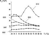
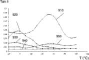
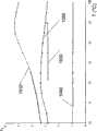
-图8到图10分别是变量Pd、tanδ和介电常数εr作为结构表面温度的函数的图示。 - Figures 8 to 10 are graphs, respectively, of the variables Pd , tan δ and the dielectric constant εr as a function of the temperature of the surface of the structure.
应当指出,为了使图更加清晰,图中所示物体的各元件不必按照比例画出。 It should be noted that, in order to improve the clarity of the drawings, the various elements of the objects shown in the drawings have not necessarily been drawn to scale. the
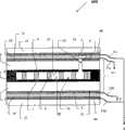
图1是平面灯1000,其由部分1组成,所述的部分1由两个由玻璃片2和3制成的基体形成,所述的玻璃片厚度例如约为4mm,部分1具有外主面21、31或第一表面,与该表面相连的是优选为连续且均匀的导电涂层4.5,二者组了一个电极,部分1还具有内表面22、32或者第二表面,所述内部表面上具有光致发光材料6、7的涂层,其例如为透明的涂层,例如可以是分散在无机基底上的荧光颗粒形式,所述的无机基底例如是硅酸锂制成的。 Figure 1 shows a planar lamp 1000 consisting of a
玻璃片2、3的第二表面22和32结合在一起,所述面上是光致发光材料6、7,二者彼此相对,并通过并通过密封釉料8连接在一起,两玻璃片之间的玻璃隔离物9使玻璃片之间形成缝隙(小于5mm)。这里,缝隙约为0.3-5mm,例如约0.4-2mm。 The second surfaces 22 and 32 of the
隔离物9可以是球形、圆柱形或立方体形,也可以是其它的几何形状,例如具有十字交叉的横断面。可以用荧光物质对隔离物进行涂覆,并至少使其侧面接触等离子气体,其中荧光物质可以与光致发光材料6、7相同或不同。 The
在两玻璃片2、3之间,是内部空间10,该内部空间10中充满减压的、通常是十分之一大气压的稀有气体,所述的稀有气体例如氙,其任选的与氖或氦混合。 Between the two
各电极都直接的沉积在基体2、3的外主面21、31上。两个电极4、5例如是氟掺杂的氧化锡层。 The electrodes are deposited directly on the outer
作为一种变型,两个电极都可以与基体进行各种方式的连接:其可以沉积在支撑电电介质的元件的外或内表面上,这种支撑电介质的元件与基体相连,从而使涂层压在基体的外主面21、31上。该元件可以例如是EVA或PVB型的一种塑料薄膜,或者是几种塑料的组合,例如PET、PVB和PU薄膜。 As a variant, both electrodes can be connected to the substrate in various ways: they can be deposited on the outer or inner surface of the element supporting the dielectric, which is connected to the substrate so that the coating compresses On the outer
各个电极还可以是与塑料薄膜结合或甚至是与基体结合的金属网格形式,这样就形成了增强的玻璃,电极还可以是相互平行的导线。 Each electrode can also be in the form of a metal grid combined with a plastic film or even a matrix, thus forming a reinforced glass, and the electrodes can also be wires parallel to each other. the
各个电极还可以夹在第一电电介质和第二电电介质之间,这些电介质与基体2、3相连。电极可以例如插在两片塑料片之间。 The individual electrodes can also be sandwiched between a first dielectric and a second dielectric, which are connected to the
电电介质的其它组合形式如下:将PVB片作为第一电电介质,其用于连接第二电电介质、例如PET片,所述第二电电介质支撑着电极,电极位于PVB片和PET片之间。 Other combinations of dielectrics are as follows: a PVB sheet is used as the first dielectric, which is used to connect a second dielectric, such as a PET sheet, and the second dielectric supports electrodes, and the electrodes are located between the PVB sheet and the PET sheet. the
电极4通过柔性垫片11a与频率为f0的高频电源相连,f0例如等于40kHz。电极4的电势为V0,数量级为1kV,频率为f0。 The
基体2、3的厚度(通常是隔开电极的电介质的厚度)越小,例如减小到2或1mm,则电压V0就必须越小,因此,为了保证绝缘而针对V和f的条件就越灵活。 The smaller the thickness of the
由柔性垫片11b支撑的电极5,其电势V1约为220V且f1为50Hz。 The
层间电介质14和保护电导体41设置在在该电极4上,其通过柔性垫片11c供电并与电极5相连。 An
保护导体41例如是一层氟掺杂的氧化烯形式,其完全沉积在玻璃片 16的内表面上,所述的玻璃片16的厚度为3.85mm,或者任选的,沉积在厚的塑料支撑体上。 The protective conductor 41 is, for example, in the form of a layer of fluorine-doped oxyalkylene deposited entirely on the inner surface of a
对于面积为0.2m2且功率为100W的电极4,通过将连续金属物体置于3.85mm厚的玻璃片16上测得的泄漏电流约为0.6mA(峰值)。 For an
绝缘体14是电容性的层合夹层,例如其至少为一种聚合物薄膜,例如其与设置在电极5上的薄膜15相同,后者将在下文进行进行说明。当表面温度为30℃、频率f0为40kHz、电极4的面积是0.2m2且功率P为100W时: The
-为了限制电容C,如果膜14是5mm厚的PVB、PU或PET膜,则功率Pd约为35W; - In order to limit the capacitance C, if the
-如果膜14是3.8mm厚的EVA薄膜,则功率Pd约为18W; - If the
-如果膜14是4mm厚的PVC膜与1.6mm厚的EVA薄膜的组合,则功率Pd约为13W; - If the
-如果膜14是4mm厚的空气(此种情况使用一个或多个隔离物和/或外围密封),则功率Pd约为11W;或者如果膜14是2mm厚的空气(2mm厚的空气相当于9mm厚的PVB)和3.15mm厚的玻璃,则功率Pd约为5W。 - if the
在这些条件下: Under these conditions:
-如果膜14是5mm厚的PVB薄膜,那么介电常数εr约为4;且 - if the
-如果膜14是3.8mm厚的EVA薄膜,那么介电常数εr约为3.5。 - If the
在这些条件下: Under these conditions:
-为了限制电容C,如果膜14是5mm厚的PVB薄膜,那么tanδ约为0.06; - In order to limit the capacitance C, if the
-如果膜14是3.8mm厚的EVA薄膜,那么tanδ约为0.018; - If the
-如果膜14是4mm厚的PVC膜与1.6mm厚的EVA薄膜的组合,那么tanδ约为0.008; - If the
-如果膜14是4mm厚的空气(2mm厚的空气相当于9mm厚的PVB),那么tanδ约为0.005;或者如果膜14是2mm厚的空气和3.15mm厚的玻璃,那么tanδ约为0.012。 - If the
穿过夹层电介质14端部的电压U等于V0-V1。 The voltage U across the ends of the
将合适的树脂或透明塑料薄膜15设置在外主面31上,所述的塑料薄膜例如由厚度为1.5mm的PVB或EVA制成,其作为与玻璃基体层合在一起的夹层,所述的玻璃基体例如厚度为3.15mm厚的玻璃片17,或者用厚的硬质塑料支撑体替代。 A suitable resin or
当电极5的面积为0.2m2且功率为100W时,通过将连续金属物体置于3.15mm厚的玻璃片176上测得的泄漏电流约为0.65mA(峰值)。 When the
如果金属物体具有更小的面积,那么泄漏电流将会按比例减小。 If the metal object has a smaller area, then the leakage current will decrease proportionally. the
在关于提高安全性的第一种变型中,V1是地电位,该地电位在灯的供电回路中的一点提供,此时泄漏电流为0。 In a first variant with regard to increased safety,V1 is the ground potential provided at a point in the supply circuit of the lamp where the leakage current is zero.
在关于提高安全性的第二种变型中,电极5和保护电导体41不相连。例如,导体41保持在V1,而第二电极与220V/50Hz的电源相连或接地。 In a second variant with regard to increased safety, the
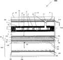
在图2所示的实施方式中,灯结构2000基本上重复了图1所示的结构,只有以下几点不同: In the embodiment shown in Figure 2, the
-保护电导体42,其为网格状,处于增强玻璃161中,电极上的玻璃厚度例如约为3mm; - Protective
-电极5的配置,其设置在膜上,所述的膜例如是与PVB或EVA薄膜相结合的PET薄膜,从而与3.85mm厚的玻璃17相接;和 - the configuration of the
-不透明的光致发光材料61、71,其只是设置在边界处,用以区分照度。 - An
电极5和导体42都接地。夹层电介质14包括2mm厚的气体层141(位于外围密封8′之间)和3mm厚的玻璃,所述气体例如空气或氮气。层间电介质14两端之间的电压U等于V0。 Both
在图3所示的实施方式中,灯结构3000基本上重复了图1所示的结构,只有以下几点不同: In the embodiment shown in Figure 3, the
-保护电导体43的配置,其覆盖在层间电介质14上,对于这种导体43,其可以进一步由粘合性薄膜提供保护,所述的薄膜例如聚氨酯膜和聚碳酸酯膜; - the configuration of the protective
-电介质14,其包括在上的1.6mm厚EVA片142和在下的4mm厚PC片143;和 - a dielectric 14 comprising an upper 1.6mm
-没有层合的玻璃罩和电极5上的塑料夹层薄膜。 - No laminated glass cover and plastic interlayer film on
由于电极5和电导体43都接地,所以电导体43就是一个屏蔽。层间电介质14两端之间的电压U等于V0。 Since both the
在图4所示的实施方式中,灯结构4000基本上重复了图1所示的结构,除了以下几点不同:电极4的电势V+约为300V,电极5的反电势V-约为700V,频率f0约为50kHz。该结构还使用了两个保护电导体44、44′,它们都是连续的透明导电层形式。两个保护电导体4、44′都与灯供电回路中的接地线相连,以避免发生任何的泄漏电流。 In the embodiment shown in FIG. 4, the
于是,层间电介质就分为两部分14、14′,例如为PVB薄膜形式,两部分的厚度例如都为2.5mm;或者也可以是上述任何其它薄膜形式。消耗功率Pd相当于两部分14、14′的端部功率之和。层间电介质两部分14、14′端部的电压U等于V+和V-。 The interlayer dielectric is then divided into two
在图5所示的实施方式中,灯结构5000基本上重复了图1所示的结构。 In the embodiment shown in FIG. 5 , the
电极5的电势V0的数量级为1kV,并处于40-50kHz的高频率。电极4的电势Vref约为220V,频率f为50Hz,并通过层间电介质140层合在一起。 The potential V0 of the
在电极5之下,装配的是可逆电化学反射器100,其能够增强结构的安全性。 Below the
该可逆电化学反射器顺次包括: The reversible electrochemical reflector includes in sequence:
-层间电介质14,其由EVA薄膜144和PC薄膜101形成; -
-第一电极102; - a
-第一成核点(nucleation sites)103,例如由铂制成; - first nucleation sites (nucleation sites) 103, for example made of platinum;
-电解质104,例如溶解在γ-丁内酯溶剂中的AgI和LiBr; -
-第二成核点105,例如由铂制成; -
-第二电极106; -
-透明基体,优选为玻璃片107,或者作为变型,使用透明的塑料基体或任何柔性或硬质组合基体;和 - a transparent substrate, preferably a
-任选的,低发射性或日光控制层108。 - Optional, low emissivity or
第一成核点103较近,而第二成核点105较远。金属材料优选为银, 其原子M+可以通过电沉积在第一点103上形成反射面109或半反射面(中间状态),或在第二点105上以导电微区的形式形成基本透明的表面(未示出)。 The
还提供了调节反射面水平或反射的装置(未示出),该装置通过校正电压、测量电流量或测量电阻来实现调节。 Means (not shown) for adjusting the level or reflection of the reflective surface are also provided by correcting the voltage, measuring the amount of current or measuring the resistance. the
由于电极102或106都接地(未示出),所以电极5的泄漏电流为0。层间电介质14两端之间的电压U等于V0-Vref。 Since both
图6所示的实施方式中,灯结构6000基本上重复了图1所示的结构,除了UV灯6000有所不同,其具有单独的发射面31(射线用宽箭头表示),而且等离子气体6′作为UV源,处于内部空间10中。 In the embodiment shown in FIG. 6, the
由于壁2′、3′选用UV-透明性材料,因此就将例如由铝制成的UV-反射器82设置在壁2′的内表面上。 Since the walls 2', 3' are made of UV-transparent material, a UV-
电极5′是带状的(或者是线状和/或网格状的),以使UV射线穿过,并且由于其没有涂层,所以像保护导体45一样接地。层间电介质14两端之间的电压U等于V0。 The electrode 5' is strip-like (or wire-like and/or grid-like) to let the UV rays pass through and, since it is not coated, is grounded like a
在图7所示的实施方式中,结构7000部分的重复了图1所示的结构,除了UV灯6000有所不同,其具有两个发射面(射线由两个宽箭头表示),等离子气体6′作为UV源,处于内部空间10中。 In the embodiment shown in FIG. 7 , the structure 7000 partially repeats the structure shown in FIG. 1 , except that the
壁2′、3′选用UV-透明性材料,与覆盖电介质162一样。保护导体46和电极4′、5′例如是带形的(或者是线状和/或网格状的),以使UV射线穿过,并且层间电介质14是氮气并具有外围密封8′。层间电介质14两端之间的电压U等于V0。 The walls 2', 3' are made of UV-transparent material, as is the covering dielectric 162. The guard conductor 46 and the electrodes 4', 5' are for example strip-shaped (or wire and/or grid-shaped) to let UV rays pass through, and the
电极5′由于没有涂层,所以像保护导体46一样接地。 The electrode 5' is grounded like a protective conductor 46 since it is not coated. the
图8到图10分别示出: Figure 8 to Figure 10 show respectively:
-作为结构1000表面温度的函数的变量Pd(曲线810-850); - the variablePd as a function of the surface temperature of the structure 1000 (curves 810-850);
-作为结构1000表面温度的函数的变量tanδ(曲线910-950); - the variable tan δ as a function of the surface temperature of the structure 1000 (curves 910-950);
-作为结构1000表面温度的函数的变量介电常数εr(曲线1010-1040); - the variable permittivity εr as a function of the surface temperature of the structure 1000 (curves 1010-1040);
这是针对下列层间电介质得到的: This is obtained for the following interlayer dielectrics:
-5mm厚的PVB层(曲线810、910、1010) -5mm thick PVB layer (
-3.8mm厚的EVA层(曲线820、920、1020); -3.8mm thick EVA layer (
-单独的PC层(曲线1030)或4mm厚的PC层与1.6mm厚的EVA层的组合层(曲线830、930); - PC layer alone (curve 1030) or a combined layer of 4 mm thick PC layer and 1.6 mm thick EVA layer (
-单独的4mm厚空气层(曲线840、940、1040); - Separate 4mm thick air layer (
-2mm厚的空气层和3.15mm厚的玻璃(曲线850、950)。 - 2mm thick air layer and 3.15mm thick glass (
可以看出,EVA比PVB具有更好的表现,尤其是在30℃以上时,此时每100W中消耗功率Pd为10-20W。 It can be seen that EVA has better performance than PVB, especially when the temperature is above 30°C, the power consumptionPd per 100W is 10-20W.
EVA/PC的组合是更加有利的,其给出了很低的消耗功率Pd,该消耗功率随温度相对保持恒定(每100W为10-17W)。 The combination EVA/PC is even more advantageous, which gives a very low power consumption Pd , which remains relatively constant with temperature (10-17 W per 100 W).
从电学观点出发,空气和空气/玻璃的组合也是有利的,这是由于其具有低的消耗功率Pd(每100W小于5W),并且具有很高的温度稳定性。即使空气/玻璃组合的损耗角相对较高,在其端部的消耗功率也很低,这是由于其电容值是所测试的绝缘体中最低的。 Air and air/glass combinations are also advantageous from an electrical point of view due to their low power dissipationPd (less than 5W per 100W) and high temperature stability. Even though the air/glass combination has a relatively high loss angle, the power dissipated at its tip is low due to its capacitance being the lowest of the insulators tested.
上述的实施例不构成对本发明的限制。 The above-mentioned embodiments do not limit the present invention. the
对于所有的不对称设计和替代组合形式,可以发生在任意电极上(选择材料、形状、玻璃或塑料的组成、等等),任意保护电导体上(选择材料、形状、玻璃或塑料的组成、等等),或者是任意层间电介质(选择材料、厚度、形状、尤其是全部面积的、或有孔结构的或不连续结构的,等等)。 For all asymmetrical designs and alternative combinations that can occur on any electrode (choice of material, shape, composition of glass or plastic, etc.), on any protective electrical conductor (choice of material, shape, composition of glass or plastic, etc.), or any interlayer dielectric (selection of material, thickness, shape, especially of the entire area, or of a porous or discontinuous structure, etc.). the
发光结构1000-5000可以形成双层玻璃窗的主要部分,例如替换窗户中的一个玻璃面。在这种结构中,可以进一步在双层玻璃窗的另一玻璃面上设置电导体。 The light emitting structures 1000-5000 may form an integral part of a double glazed window, for example replacing one pane of glass in the window. In this structure, an electric conductor can further be provided on the other glass face of the double-glazed window. the
当利用等离子气体活化时,光致发光材料在特定区域的不同分布,使得可以将该区域的等离子体能量转化为可见光辐射,从而形成发光区域(依赖于光致发光材料的性质,其自身可以是不透明的或透明的)。 When activated with a plasma gas, the different distribution of the photoluminescent material in a specific area makes it possible to convert the plasma energy in that area into visible light radiation, thereby forming a light-emitting area (depending on the nature of the photoluminescent material, which itself can be opaque or transparent). the
发光区域还可以形成一系列几何图形(线、点、圆圈、方块或其他任意形状),并且图形之间的空间和/或图形的尺寸是可以调节的。 The light-emitting area can also form a series of geometric figures (lines, dots, circles, squares or other arbitrary shapes), and the space between the figures and/or the size of the figures can be adjusted. the
壁可以是任意形状,其轮廓可以是多边形、凹陷或凸起的,尤其可以是方形或矩形的,或者是曲线形的,具有可变或恒定的曲率半径,其尤其可以是圆形或椭圆形的。 The walls can be of any shape, their contours can be polygonal, concave or convex, especially square or rectangular, or curved, with a variable or constant radius of curvature, which can especially be circular or oval of. the
壁可以是平面或曲面,优选保持恒定的分离距离。 The walls can be flat or curved, preferably maintaining a constant separation distance. the
壁可以是具有光学效果的玻璃基底,壁尤其可以是彩色的、装饰性的、结构性的、散射性的,等等。 The walls can be glass substrates with an optical effect, the walls can in particular be coloured, decorative, structural, diffuse, etc. the
可以通过矿物手段(例如玻璃釉料)、通过基本透明的材料(玻璃等等)、或使用粘合剂(硅酮)对结构进行密封。 The structure can be sealed by mineral means (such as glass frit), by a substantially transparent material (glass, etc.), or with an adhesive (silicone). the
Claims (14)
Translated fromChineseApplications Claiming Priority (3)
| Application Number | Priority Date | Filing Date | Title |
|---|---|---|---|
| FR0653414AFR2905032A1 (en) | 2006-08-21 | 2006-08-21 | SENSITIVELY FLAT LUMINOUS AND / OR UV STRUCTURE |
| FR0653414 | 2006-08-21 | ||
| PCT/FR2007/051719WO2008023124A1 (en) | 2006-08-21 | 2007-07-25 | Substantially flat luminous and/or uv structure |
Publications (2)
| Publication Number | Publication Date |
|---|---|
| CN101785081A CN101785081A (en) | 2010-07-21 |
| CN101785081Btrue CN101785081B (en) | 2012-04-18 |
Family
ID=37719460
Family Applications (1)
| Application Number | Title | Priority Date | Filing Date |
|---|---|---|---|
| CN200780053652XAExpired - Fee RelatedCN101785081B (en) | 2006-08-21 | 2007-07-25 | Substantially planar light-emitting and/or UV-emitting structures |
Country Status (12)
| Country | Link |
|---|---|
| US (1) | US8120236B2 (en) |
| EP (1) | EP2070103B1 (en) |
| JP (1) | JP2010501975A (en) |
| KR (1) | KR20090042984A (en) |
| CN (1) | CN101785081B (en) |
| AT (1) | ATE500605T1 (en) |
| DE (1) | DE602007012911D1 (en) |
| ES (1) | ES2362446T3 (en) |
| FR (1) | FR2905032A1 (en) |
| PT (1) | PT2070103E (en) |
| TW (1) | TW200823956A (en) |
| WO (1) | WO2008023124A1 (en) |
Families Citing this family (138)
| Publication number | Priority date | Publication date | Assignee | Title |
|---|---|---|---|---|
| US7806543B2 (en) | 2007-01-03 | 2010-10-05 | Hill Phoenix, Inc. | Light system for a temperature controlled case |
| FR2915314B1 (en)* | 2007-04-17 | 2011-04-22 | Saint Gobain | UV FLOOR LAMP WITH DISCHARGES AND USES. |
| FR2915311B1 (en)* | 2007-04-17 | 2011-01-07 | Saint Gobain | FLASHLIGHT WITH DISCHARGE. |
| FR2936360B1 (en) | 2008-09-24 | 2011-04-01 | Saint Gobain | PROCESS FOR MANUFACTURING A MASK WITH SUBMILLIMETRIC OPENINGS FOR SUBMILLIMETRIC ELECTROCONDUCTIVE GRID, MASK AND SUBMILLIMETRIC ELECTROCONDUCTIVE GRID. |
| FR2936358B1 (en) | 2008-09-24 | 2011-01-21 | Saint Gobain | PROCESS FOR MANUFACTURING SUBMILLIMETRIC MOLDED MASKS FOR SUBMILLIMETRIC ELECTROCONDUCTIVE GRID, SUBMILLIMETRIC MOLDING MASK, SUBMILLIMETRIC ELECTROCONDUCTIVE GRID. |
| FR2936362B1 (en) | 2008-09-25 | 2010-09-10 | Saint Gobain | METHOD FOR MANUFACTURING AN ELECTROCONDUCTIVE SUBMILLIMETRIC GRID COATED WITH A SURGRILLE GRID, ELECTROCONDUCTIVE SUBMILLIMETER GRID COVERED WITH AN OVERGRILL |
| FR2939006B1 (en) | 2008-11-26 | 2010-11-12 | Saint Gobain | BALLAST PULSE FOR FLAT LAMPS |
| US8164818B2 (en) | 2010-11-08 | 2012-04-24 | Soladigm, Inc. | Electrochromic window fabrication methods |
| TWI442446B (en)* | 2011-04-19 | 2014-06-21 | Ind Tech Res Inst | Light-emitting element and display device |
| US12321075B2 (en) | 2011-12-12 | 2025-06-03 | View Operating Corporation | Electrochromic laminates |
| US10739658B2 (en) | 2011-12-12 | 2020-08-11 | View, Inc. | Electrochromic laminates |
| US8998469B1 (en) | 2013-01-08 | 2015-04-07 | Ruth M. Miller | Lighted ceramic tile assembly |
| CN103200290A (en)* | 2013-03-20 | 2013-07-10 | 上海鼎为软件技术有限公司 | Mobile terminal |
| US9905743B2 (en) | 2013-11-21 | 2018-02-27 | Ford Global Technologies, Llc | Printed LED heat sink double lock |
| US10064256B2 (en) | 2013-11-21 | 2018-08-28 | Ford Global Technologies, Llc | System and method for remote activation of vehicle lighting |
| US9868387B2 (en) | 2013-11-21 | 2018-01-16 | Ford Global Technologies, Llc | Photoluminescent printed LED molding |
| US9961745B2 (en) | 2013-11-21 | 2018-05-01 | Ford Global Technologies, Llc | Printed LED rylene dye welcome/farewell lighting |
| US9810401B2 (en) | 2013-11-21 | 2017-11-07 | Ford Global Technologies, Llc | Luminescent trim light assembly |
| US9809160B2 (en) | 2013-11-21 | 2017-11-07 | Ford Global Technologies, Llc | Tailgate illumination system |
| US9796325B2 (en) | 2013-11-21 | 2017-10-24 | Ford Global Technologies, Llc | Exterior light system for a vehicle |
| US9931991B2 (en) | 2013-11-21 | 2018-04-03 | Ford Global Technologies, Llc | Rotating garment hook |
| US10400978B2 (en) | 2013-11-21 | 2019-09-03 | Ford Global Technologies, Llc | Photoluminescent lighting apparatus for vehicles |
| US9821708B2 (en) | 2013-11-21 | 2017-11-21 | Ford Global Technologies, Llc | Illuminated exterior strip |
| US9849831B2 (en) | 2013-11-21 | 2017-12-26 | Ford Global Technologies, Llc | Printed LED storage compartment |
| US9950658B2 (en) | 2013-11-21 | 2018-04-24 | Ford Global Technologies, Llc | Privacy window system |
| US9797575B2 (en) | 2013-11-21 | 2017-10-24 | Ford Global Technologies, Llc | Light-producing assembly for a vehicle |
| US9902320B2 (en) | 2013-11-21 | 2018-02-27 | Ford Global Technologies, Llc | Photoluminescent color changing dome map lamp |
| US9839098B2 (en) | 2013-11-21 | 2017-12-05 | Ford Global Technologies, Llc | Light assembly operable as a dome lamp |
| US9796304B2 (en) | 2013-11-21 | 2017-10-24 | Ford Global Technologies, Llc | Vehicle floor lighting system having a pivotable base with light-producing assembly coupled to base |
| US10363867B2 (en) | 2013-11-21 | 2019-07-30 | Ford Global Technologies, Llc | Printed LED trim panel lamp |
| US10041650B2 (en) | 2013-11-21 | 2018-08-07 | Ford Global Technologies, Llc | Illuminated instrument panel storage compartment |
| US9989216B2 (en) | 2013-11-21 | 2018-06-05 | Ford Global Technologies, Llc | Interior exterior moving designs |
| US9539940B2 (en) | 2013-11-21 | 2017-01-10 | Ford Global Technologies, Llc | Illuminated indicator |
| US9969323B2 (en) | 2013-11-21 | 2018-05-15 | Ford Global Technologies, Llc | Vehicle lighting system employing a light strip |
| US9782504B2 (en)* | 2013-11-21 | 2017-10-10 | Ford Global Technologies, Inc. | Self-disinfecting surface with printed LEDs for a surface of a vehicle |
| RU2713535C2 (en)* | 2015-06-10 | 2020-02-05 | ФОРД ГЛОУБАЛ ТЕКНОЛОДЖИЗ, ЭлЭлСи | Self-insulating surface coating of vehicle |
| US10168039B2 (en) | 2015-08-10 | 2019-01-01 | Ford Global Technologies, Llc | Illuminated badge for a vehicle |
| US9889791B2 (en) | 2015-12-01 | 2018-02-13 | Ford Global Technologies, Llc | Illuminated badge for a vehicle |
| US10023100B2 (en) | 2015-12-14 | 2018-07-17 | Ford Global Technologies, Llc | Illuminated trim assembly |
| US10300843B2 (en) | 2016-01-12 | 2019-05-28 | Ford Global Technologies, Llc | Vehicle illumination assembly |
| US10501007B2 (en) | 2016-01-12 | 2019-12-10 | Ford Global Technologies, Llc | Fuel port illumination device |
| US10235911B2 (en) | 2016-01-12 | 2019-03-19 | Ford Global Technologies, Llc | Illuminating badge for a vehicle |
| US9855799B2 (en) | 2016-02-09 | 2018-01-02 | Ford Global Technologies, Llc | Fuel level indicator |
| US10011219B2 (en) | 2016-01-18 | 2018-07-03 | Ford Global Technologies, Llc | Illuminated badge |
| US9927114B2 (en) | 2016-01-21 | 2018-03-27 | Ford Global Technologies, Llc | Illumination apparatus utilizing conductive polymers |
| US9586519B1 (en) | 2016-01-27 | 2017-03-07 | Ford Global Technologies, Llc | Vehicle rear illumination |
| US10189401B2 (en) | 2016-02-09 | 2019-01-29 | Ford Global Technologies, Llc | Vehicle light strip with optical element |
| US9656598B1 (en) | 2016-02-23 | 2017-05-23 | Ford Global Technologies, Llc | Vehicle badge |
| US9751458B1 (en) | 2016-02-26 | 2017-09-05 | Ford Global Technologies, Llc | Vehicle illumination system |
| US10501025B2 (en) | 2016-03-04 | 2019-12-10 | Ford Global Technologies, Llc | Vehicle badge |
| US10118568B2 (en) | 2016-03-09 | 2018-11-06 | Ford Global Technologies, Llc | Vehicle badge having discretely illuminated portions |
| US9963001B2 (en) | 2016-03-24 | 2018-05-08 | Ford Global Technologies, Llc | Vehicle wheel illumination assembly using photoluminescent material |
| US10081296B2 (en) | 2016-04-06 | 2018-09-25 | Ford Global Technologies, Llc | Illuminated exterior strip with photoluminescent structure and retroreflective layer |
| US9902315B2 (en) | 2016-04-15 | 2018-02-27 | Ford Global Technologies, Llc | Photoluminescent lighting apparatus for vehicles |
| US9738219B1 (en) | 2016-05-11 | 2017-08-22 | Ford Global Technologies, Llc | Illuminated vehicle trim |
| US10064259B2 (en) | 2016-05-11 | 2018-08-28 | Ford Global Technologies, Llc | Illuminated vehicle badge |
| US10420189B2 (en) | 2016-05-11 | 2019-09-17 | Ford Global Technologies, Llc | Vehicle lighting assembly |
| US10631373B2 (en) | 2016-05-12 | 2020-04-21 | Ford Global Technologies, Llc | Heated windshield indicator |
| US9821710B1 (en) | 2016-05-12 | 2017-11-21 | Ford Global Technologies, Llc | Lighting apparatus for vehicle decklid |
| US9994144B2 (en) | 2016-05-23 | 2018-06-12 | Ford Global Technologies, Llc | Illuminated automotive glazings |
| US9896020B2 (en) | 2016-05-23 | 2018-02-20 | Ford Global Technologies, Llc | Vehicle lighting assembly |
| US9925917B2 (en) | 2016-05-26 | 2018-03-27 | Ford Global Technologies, Llc | Concealed lighting for vehicles |
| US9937855B2 (en) | 2016-06-02 | 2018-04-10 | Ford Global Technologies, Llc | Automotive window glazings |
| US9803822B1 (en) | 2016-06-03 | 2017-10-31 | Ford Global Technologies, Llc | Vehicle illumination assembly |
| US10343622B2 (en) | 2016-06-09 | 2019-07-09 | Ford Global Technologies, Llc | Interior and exterior iridescent vehicle appliques |
| US10205338B2 (en) | 2016-06-13 | 2019-02-12 | Ford Global Technologies, Llc | Illuminated vehicle charging assembly |
| US10131237B2 (en) | 2016-06-22 | 2018-11-20 | Ford Global Technologies, Llc | Illuminated vehicle charging system |
| US9855888B1 (en) | 2016-06-29 | 2018-01-02 | Ford Global Technologies, Llc | Photoluminescent vehicle appliques |
| US9840191B1 (en) | 2016-07-12 | 2017-12-12 | Ford Global Technologies, Llc | Vehicle lamp assembly |
| US9855797B1 (en) | 2016-07-13 | 2018-01-02 | Ford Global Technologies, Llc | Illuminated system for a vehicle |
| US9889801B2 (en) | 2016-07-14 | 2018-02-13 | Ford Global Technologies, Llc | Vehicle lighting assembly |
| US9840193B1 (en) | 2016-07-15 | 2017-12-12 | Ford Global Technologies, Llc | Vehicle lighting assembly |
| US9845047B1 (en) | 2016-08-08 | 2017-12-19 | Ford Global Technologies, Llc | Light system |
| US9827903B1 (en) | 2016-08-18 | 2017-11-28 | Ford Global Technologies, Llc | Illuminated trim panel |
| US10173604B2 (en) | 2016-08-24 | 2019-01-08 | Ford Global Technologies, Llc | Illuminated vehicle console |
| US10047659B2 (en) | 2016-08-31 | 2018-08-14 | Ford Global Technologies, Llc | Photoluminescent engine indicium |
| US10047911B2 (en) | 2016-08-31 | 2018-08-14 | Ford Global Technologies, Llc | Photoluminescent emission system |
| US10065555B2 (en) | 2016-09-08 | 2018-09-04 | Ford Global Technologies, Llc | Directional approach lighting |
| US10075013B2 (en) | 2016-09-08 | 2018-09-11 | Ford Global Technologies, Llc | Vehicle apparatus for charging photoluminescent utilities |
| US10308175B2 (en) | 2016-09-08 | 2019-06-04 | Ford Global Technologies, Llc | Illumination apparatus for vehicle accessory |
| US10043396B2 (en) | 2016-09-13 | 2018-08-07 | Ford Global Technologies, Llc | Passenger pickup system and method using autonomous shuttle vehicle |
| US9863171B1 (en) | 2016-09-28 | 2018-01-09 | Ford Global Technologies, Llc | Vehicle compartment |
| US10137829B2 (en) | 2016-10-06 | 2018-11-27 | Ford Global Technologies, Llc | Smart drop off lighting system |
| US10046688B2 (en) | 2016-10-06 | 2018-08-14 | Ford Global Technologies, Llc | Vehicle containing sales bins |
| US9914390B1 (en) | 2016-10-19 | 2018-03-13 | Ford Global Technologies, Llc | Vehicle shade assembly |
| US10086700B2 (en) | 2016-10-20 | 2018-10-02 | Ford Global Technologies, Llc | Illuminated switch |
| US9802534B1 (en) | 2016-10-21 | 2017-10-31 | Ford Global Technologies, Llc | Illuminated vehicle compartment |
| US10035473B2 (en) | 2016-11-04 | 2018-07-31 | Ford Global Technologies, Llc | Vehicle trim components |
| US9902314B1 (en) | 2016-11-17 | 2018-02-27 | Ford Global Technologies, Llc | Vehicle light system |
| US10220784B2 (en) | 2016-11-29 | 2019-03-05 | Ford Global Technologies, Llc | Luminescent windshield display |
| US9994089B1 (en) | 2016-11-29 | 2018-06-12 | Ford Global Technologies, Llc | Vehicle curtain |
| US10106074B2 (en) | 2016-12-07 | 2018-10-23 | Ford Global Technologies, Llc | Vehicle lamp system |
| US10118538B2 (en) | 2016-12-07 | 2018-11-06 | Ford Global Technologies, Llc | Illuminated rack |
| US10422501B2 (en) | 2016-12-14 | 2019-09-24 | Ford Global Technologies, Llc | Vehicle lighting assembly |
| US10144365B2 (en) | 2017-01-10 | 2018-12-04 | Ford Global Technologies, Llc | Vehicle badge |
| US9815402B1 (en) | 2017-01-16 | 2017-11-14 | Ford Global Technologies, Llc | Tailgate and cargo box illumination |
| US10173582B2 (en) | 2017-01-26 | 2019-01-08 | Ford Global Technologies, Llc | Light system |
| US10053006B1 (en) | 2017-01-31 | 2018-08-21 | Ford Global Technologies, Llc | Illuminated assembly |
| US9849830B1 (en) | 2017-02-01 | 2017-12-26 | Ford Global Technologies, Llc | Tailgate illumination |
| US9896023B1 (en) | 2017-02-09 | 2018-02-20 | Ford Global Technologies, Llc | Vehicle rear lighting assembly |
| US10427593B2 (en) | 2017-02-09 | 2019-10-01 | Ford Global Technologies, Llc | Vehicle light assembly |
| US9849829B1 (en) | 2017-03-02 | 2017-12-26 | Ford Global Technologies, Llc | Vehicle light system |
| US9758090B1 (en) | 2017-03-03 | 2017-09-12 | Ford Global Technologies, Llc | Interior side marker |
| US10240737B2 (en) | 2017-03-06 | 2019-03-26 | Ford Global Technologies, Llc | Vehicle light assembly |
| US10399483B2 (en) | 2017-03-08 | 2019-09-03 | Ford Global Technologies, Llc | Vehicle illumination assembly |
| US10150396B2 (en) | 2017-03-08 | 2018-12-11 | Ford Global Technologies, Llc | Vehicle cup holder assembly with photoluminescent accessory for increasing the number of available cup holders |
| US10195985B2 (en) | 2017-03-08 | 2019-02-05 | Ford Global Technologies, Llc | Vehicle light system |
| US10611298B2 (en) | 2017-03-13 | 2020-04-07 | Ford Global Technologies, Llc | Illuminated cargo carrier |
| US10166913B2 (en) | 2017-03-15 | 2019-01-01 | Ford Global Technologies, Llc | Side marker illumination |
| US10483678B2 (en) | 2017-03-29 | 2019-11-19 | Ford Global Technologies, Llc | Vehicle electrical connector |
| US10569696B2 (en) | 2017-04-03 | 2020-02-25 | Ford Global Technologies, Llc | Vehicle illuminated airflow control device |
| US10035463B1 (en) | 2017-05-10 | 2018-07-31 | Ford Global Technologies, Llc | Door retention system |
| US10399486B2 (en) | 2017-05-10 | 2019-09-03 | Ford Global Technologies, Llc | Vehicle door removal and storage |
| US9963066B1 (en) | 2017-05-15 | 2018-05-08 | Ford Global Technologies, Llc | Vehicle running board that provides light excitation |
| US10059238B1 (en) | 2017-05-30 | 2018-08-28 | Ford Global Technologies, Llc | Vehicle seating assembly |
| US10144337B1 (en) | 2017-06-02 | 2018-12-04 | Ford Global Technologies, Llc | Vehicle light assembly |
| US10493904B2 (en) | 2017-07-17 | 2019-12-03 | Ford Global Technologies, Llc | Vehicle light assembly |
| US10502690B2 (en) | 2017-07-18 | 2019-12-10 | Ford Global Technologies, Llc | Indicator system for vehicle wear components |
| US10137831B1 (en) | 2017-07-19 | 2018-11-27 | Ford Global Technologies, Llc | Vehicle seal assembly |
| US10160405B1 (en) | 2017-08-22 | 2018-12-25 | Ford Global Technologies, Llc | Vehicle decal assembly |
| US10186177B1 (en) | 2017-09-13 | 2019-01-22 | Ford Global Technologies, Llc | Vehicle windshield lighting assembly |
| US10137825B1 (en) | 2017-10-02 | 2018-11-27 | Ford Global Technologies, Llc | Vehicle lamp assembly |
| US10391943B2 (en) | 2017-10-09 | 2019-08-27 | Ford Global Technologies, Llc | Vehicle lamp assembly |
| US10207636B1 (en) | 2017-10-18 | 2019-02-19 | Ford Global Technologies, Llc | Seatbelt stowage assembly |
| US10189414B1 (en) | 2017-10-26 | 2019-01-29 | Ford Global Technologies, Llc | Vehicle storage assembly |
| US10723258B2 (en) | 2018-01-04 | 2020-07-28 | Ford Global Technologies, Llc | Vehicle lamp assembly |
| US10723257B2 (en) | 2018-02-14 | 2020-07-28 | Ford Global Technologies, Llc | Multi-color luminescent grille for a vehicle |
| US10627092B2 (en) | 2018-03-05 | 2020-04-21 | Ford Global Technologies, Llc | Vehicle grille assembly |
| US10281113B1 (en) | 2018-03-05 | 2019-05-07 | Ford Global Technologies, Llc | Vehicle grille |
| US10457196B1 (en) | 2018-04-11 | 2019-10-29 | Ford Global Technologies, Llc | Vehicle light assembly |
| US10703263B2 (en) | 2018-04-11 | 2020-07-07 | Ford Global Technologies, Llc | Vehicle light system |
| US10778223B2 (en) | 2018-04-23 | 2020-09-15 | Ford Global Technologies, Llc | Hidden switch assembly |
| US10576893B1 (en) | 2018-10-08 | 2020-03-03 | Ford Global Technologies, Llc | Vehicle light assembly |
| US10720551B1 (en) | 2019-01-03 | 2020-07-21 | Ford Global Technologies, Llc | Vehicle lamps |
| JP7484463B2 (en)* | 2020-06-12 | 2024-05-16 | 東芝ライテック株式会社 | Ultraviolet irradiation equipment |
| US20220152233A1 (en)* | 2020-11-19 | 2022-05-19 | Palo Alto Research Center Incorporated | Integrated uv disinfection |
| JPWO2022210251A1 (en)* | 2021-03-29 | 2022-10-06 | ||
| CN115692164A (en)* | 2022-10-21 | 2023-02-03 | 朗升光电科技(广东)有限公司 | Improved ultraviolet lamp |
Citations (3)
| Publication number | Priority date | Publication date | Assignee | Title |
|---|---|---|---|---|
| CN1154566A (en)* | 1995-10-02 | 1997-07-16 | 奥斯兰姆施尔凡尼亚公司 | Discharge lamp having light-transmissive conductive coating for RF containment and heating |
| US6340866B1 (en)* | 1998-02-05 | 2002-01-22 | Lg Electronics Inc. | Plasma display panel and driving method thereof |
| EP1180781A2 (en)* | 2000-08-10 | 2002-02-20 | Nisshinbo Industries Inc. | Front plate for plasma display panels, and method of producing the same |
Family Cites Families (12)
| Publication number | Priority date | Publication date | Assignee | Title |
|---|---|---|---|---|
| CH473354A (en)* | 1968-11-12 | 1969-05-31 | Sulzer Ernst | Anti-glare housing for lighting |
| US3999057A (en)* | 1975-03-03 | 1976-12-21 | Martin Hamacher | Lighting structure |
| JPH0212751A (en)* | 1988-06-30 | 1990-01-17 | Toshiba Lighting & Technol Corp | High-frequency lighting type fluorescent lamp |
| US5319282A (en)* | 1991-12-30 | 1994-06-07 | Winsor Mark D | Planar fluorescent and electroluminescent lamp having one or more chambers |
| JPH06349450A (en)* | 1993-06-08 | 1994-12-22 | Sony Corp | Planar phosphor tube |
| JPH07288102A (en)* | 1994-04-18 | 1995-10-31 | Nippon Sheet Glass Co Ltd | Flat-panel fluorescent lamp |
| JPH11143372A (en)* | 1997-11-07 | 1999-05-28 | Matsushita Electric Ind Co Ltd | Plasma display shield structure |
| JP2003107463A (en)* | 2001-09-26 | 2003-04-09 | Hitachi Ltd | Liquid crystal display |
| JP3876170B2 (en)* | 2002-02-25 | 2007-01-31 | 松下電器産業株式会社 | Impact display film for flat display panel and flat display panel |
| FR2843483B1 (en)* | 2002-08-06 | 2005-07-08 | Saint Gobain | FLASHLIGHT, METHOD OF MANUFACTURE AND APPLICATION |
| JP2005302646A (en)* | 2004-04-15 | 2005-10-27 | Lecip Corp | Flat discharge tube illumination device |
| JP4583813B2 (en)* | 2004-06-03 | 2010-11-17 | Nec液晶テクノロジー株式会社 | Lamp unit and flat fluorescent lamp |
- 2006
- 2006-08-21FRFR0653414Apatent/FR2905032A1/ennot_activeWithdrawn
- 2007
- 2007-07-25DEDE602007012911Tpatent/DE602007012911D1/enactiveActive
- 2007-07-25KRKR1020097005784Apatent/KR20090042984A/ennot_activeCeased
- 2007-07-25ATAT07823636Tpatent/ATE500605T1/enactive
- 2007-07-25ESES07823636Tpatent/ES2362446T3/enactiveActive
- 2007-07-25USUS12/438,371patent/US8120236B2/ennot_activeExpired - Fee Related
- 2007-07-25PTPT07823636Tpatent/PT2070103E/enunknown
- 2007-07-25EPEP07823636Apatent/EP2070103B1/ennot_activeNot-in-force
- 2007-07-25JPJP2009525088Apatent/JP2010501975A/enactivePending
- 2007-07-25CNCN200780053652XApatent/CN101785081B/ennot_activeExpired - Fee Related
- 2007-07-25WOPCT/FR2007/051719patent/WO2008023124A1/enactiveApplication Filing
- 2007-08-02TWTW096128443Apatent/TW200823956A/enunknown
Patent Citations (3)
| Publication number | Priority date | Publication date | Assignee | Title |
|---|---|---|---|---|
| CN1154566A (en)* | 1995-10-02 | 1997-07-16 | 奥斯兰姆施尔凡尼亚公司 | Discharge lamp having light-transmissive conductive coating for RF containment and heating |
| US6340866B1 (en)* | 1998-02-05 | 2002-01-22 | Lg Electronics Inc. | Plasma display panel and driving method thereof |
| EP1180781A2 (en)* | 2000-08-10 | 2002-02-20 | Nisshinbo Industries Inc. | Front plate for plasma display panels, and method of producing the same |
Also Published As
| Publication number | Publication date |
|---|---|
| CN101785081A (en) | 2010-07-21 |
| TW200823956A (en) | 2008-06-01 |
| ES2362446T3 (en) | 2011-07-05 |
| WO2008023124A1 (en) | 2008-02-28 |
| US8120236B2 (en) | 2012-02-21 |
| JP2010501975A (en) | 2010-01-21 |
| DE602007012911D1 (en) | 2011-04-14 |
| PT2070103E (en) | 2011-06-09 |
| ATE500605T1 (en) | 2011-03-15 |
| EP2070103B1 (en) | 2011-03-02 |
| US20090322202A1 (en) | 2009-12-31 |
| KR20090042984A (en) | 2009-05-04 |
| FR2905032A1 (en) | 2008-02-22 |
| EP2070103A1 (en) | 2009-06-17 |
Similar Documents
| Publication | Publication Date | Title |
|---|---|---|
| CN101785081B (en) | Substantially planar light-emitting and/or UV-emitting structures | |
| CN101124655B (en) | Flat or roughly flat light-emitting structure | |
| US20090058295A1 (en) | Flat coplanar-discharge lamp and uses of same | |
| JP2010525508A (en) | Flat discharge lamp | |
| CN101243540A (en) | Coplanar Discharge Flat UV Lamp and Its Application | |
| CN101681797A (en) | Flat uv discharge lamp, uses and manufacture | |
| ES2425843T3 (en) | Electric thermal glass panel, manufacturing procedure, as well as window | |
| KR101044049B1 (en) | Flat lamps, methods for manufacturing the same, and methods of using the flat lamps | |
| CN101189407B (en) | Planar or substantially planar light-emitting structures | |
| TW200912995A (en) | Flat discharge lamp | |
| US20100109506A1 (en) | Laminated flat lamp and its manufacturing process |
Legal Events
| Date | Code | Title | Description |
|---|---|---|---|
| C06 | Publication | ||
| PB01 | Publication | ||
| C10 | Entry into substantive examination | ||
| SE01 | Entry into force of request for substantive examination | ||
| C14 | Grant of patent or utility model | ||
| GR01 | Patent grant | ||
| C17 | Cessation of patent right | ||
| CF01 | Termination of patent right due to non-payment of annual fee | Granted publication date:20120418 Termination date:20130725 |