CN101784390A - Actuator - Google Patents
ActuatorDownload PDFInfo
- Publication number
- CN101784390A CN101784390ACN200880101410ACN200880101410ACN101784390ACN 101784390 ACN101784390 ACN 101784390ACN 200880101410 ACN200880101410 ACN 200880101410ACN 200880101410 ACN200880101410 ACN 200880101410ACN 101784390 ACN101784390 ACN 101784390A
- Authority
- CN
- China
- Prior art keywords
- conductor
- chamber
- flexible
- actuator
- conductors
- Prior art date
- Legal status (The legal status is an assumption and is not a legal conclusion. Google has not performed a legal analysis and makes no representation as to the accuracy of the status listed.)
- Granted
Links
Images


Classifications
- B—PERFORMING OPERATIONS; TRANSPORTING
- B41—PRINTING; LINING MACHINES; TYPEWRITERS; STAMPS
- B41J—TYPEWRITERS; SELECTIVE PRINTING MECHANISMS, i.e. MECHANISMS PRINTING OTHERWISE THAN FROM A FORME; CORRECTION OF TYPOGRAPHICAL ERRORS
- B41J2/00—Typewriters or selective printing mechanisms characterised by the printing or marking process for which they are designed
- B41J2/005—Typewriters or selective printing mechanisms characterised by the printing or marking process for which they are designed characterised by bringing liquid or particles selectively into contact with a printing material
- B41J2/01—Ink jet
- B41J2/135—Nozzles
- B41J2/14—Structure thereof only for on-demand ink jet heads
- B41J2/14314—Structure of ink jet print heads with electrostatically actuated membrane
- B—PERFORMING OPERATIONS; TRANSPORTING
- B41—PRINTING; LINING MACHINES; TYPEWRITERS; STAMPS
- B41J—TYPEWRITERS; SELECTIVE PRINTING MECHANISMS, i.e. MECHANISMS PRINTING OTHERWISE THAN FROM A FORME; CORRECTION OF TYPOGRAPHICAL ERRORS
- B41J2/00—Typewriters or selective printing mechanisms characterised by the printing or marking process for which they are designed
- B41J2/005—Typewriters or selective printing mechanisms characterised by the printing or marking process for which they are designed characterised by bringing liquid or particles selectively into contact with a printing material
- B41J2/01—Ink jet
- B41J2/135—Nozzles
- B41J2/16—Production of nozzles
- B41J2/1621—Manufacturing processes
- B41J2/1626—Manufacturing processes etching
- B41J2/1628—Manufacturing processes etching dry etching
- B—PERFORMING OPERATIONS; TRANSPORTING
- B41—PRINTING; LINING MACHINES; TYPEWRITERS; STAMPS
- B41J—TYPEWRITERS; SELECTIVE PRINTING MECHANISMS, i.e. MECHANISMS PRINTING OTHERWISE THAN FROM A FORME; CORRECTION OF TYPOGRAPHICAL ERRORS
- B41J2/00—Typewriters or selective printing mechanisms characterised by the printing or marking process for which they are designed
- B41J2/005—Typewriters or selective printing mechanisms characterised by the printing or marking process for which they are designed characterised by bringing liquid or particles selectively into contact with a printing material
- B41J2/01—Ink jet
- B41J2/135—Nozzles
- B41J2/16—Production of nozzles
- B41J2/1621—Manufacturing processes
- B41J2/1631—Manufacturing processes photolithography
- B—PERFORMING OPERATIONS; TRANSPORTING
- B41—PRINTING; LINING MACHINES; TYPEWRITERS; STAMPS
- B41J—TYPEWRITERS; SELECTIVE PRINTING MECHANISMS, i.e. MECHANISMS PRINTING OTHERWISE THAN FROM A FORME; CORRECTION OF TYPOGRAPHICAL ERRORS
- B41J2/00—Typewriters or selective printing mechanisms characterised by the printing or marking process for which they are designed
- B41J2/005—Typewriters or selective printing mechanisms characterised by the printing or marking process for which they are designed characterised by bringing liquid or particles selectively into contact with a printing material
- B41J2/01—Ink jet
- B41J2/135—Nozzles
- B41J2/16—Production of nozzles
- B41J2/1621—Manufacturing processes
- B41J2/1632—Manufacturing processes machining
- B—PERFORMING OPERATIONS; TRANSPORTING
- B41—PRINTING; LINING MACHINES; TYPEWRITERS; STAMPS
- B41J—TYPEWRITERS; SELECTIVE PRINTING MECHANISMS, i.e. MECHANISMS PRINTING OTHERWISE THAN FROM A FORME; CORRECTION OF TYPOGRAPHICAL ERRORS
- B41J2/00—Typewriters or selective printing mechanisms characterised by the printing or marking process for which they are designed
- B41J2/005—Typewriters or selective printing mechanisms characterised by the printing or marking process for which they are designed characterised by bringing liquid or particles selectively into contact with a printing material
- B41J2/01—Ink jet
- B41J2/135—Nozzles
- B41J2/16—Production of nozzles
- B41J2/1621—Manufacturing processes
- B41J2/164—Manufacturing processes thin film formation
- B41J2/1642—Manufacturing processes thin film formation thin film formation by CVD [chemical vapor deposition]
- B—PERFORMING OPERATIONS; TRANSPORTING
- B41—PRINTING; LINING MACHINES; TYPEWRITERS; STAMPS
- B41J—TYPEWRITERS; SELECTIVE PRINTING MECHANISMS, i.e. MECHANISMS PRINTING OTHERWISE THAN FROM A FORME; CORRECTION OF TYPOGRAPHICAL ERRORS
- B41J2/00—Typewriters or selective printing mechanisms characterised by the printing or marking process for which they are designed
- B41J2/005—Typewriters or selective printing mechanisms characterised by the printing or marking process for which they are designed characterised by bringing liquid or particles selectively into contact with a printing material
- B41J2/01—Ink jet
- B41J2/135—Nozzles
- B41J2/16—Production of nozzles
- B41J2/1621—Manufacturing processes
- B41J2/164—Manufacturing processes thin film formation
- B41J2/1646—Manufacturing processes thin film formation thin film formation by sputtering
Landscapes
- Engineering & Computer Science (AREA)
- Manufacturing & Machinery (AREA)
- Particle Formation And Scattering Control In Inkjet Printers (AREA)
Abstract
Description
Translated fromChinese背景技术Background technique
压电致动的喷墨打印头用在非常大幅面的喷墨打印应用中,例如,大型标志图样的工业打印市场。然而,使用传统的半导体晶片制造技术却难以加工压电材料。在传统的压电致动器制造过程中,使用锯来图案化材料,以进行后续蚀刻。有时使用的锯很长,且压电特征的尺寸还受到锯加工工具的限制。Piezoelectrically actuated inkjet printheads are used in very large format inkjet printing applications, for example, the industrial printing market for large signage. However, piezoelectric materials are difficult to process using conventional semiconductor wafer fabrication techniques. In traditional piezoelectric actuator manufacturing, a saw is used to pattern the material for subsequent etching. The saws used are sometimes very long, and the size of the piezoelectric features is also limited by the sawing tool.
附图说明Description of drawings
图1是示出了喷墨打印机的一个实施例的框图。FIG. 1 is a block diagram illustrating one embodiment of an inkjet printer.
图2是一个透视图,其中示出了可以用在图1中所示的打印机的打印头阵列中的喷墨打印头的一个实施例。FIG. 2 is a perspective view showing one embodiment of an inkjet printhead that may be used in the printhead array of the printer shown in FIG. 1. FIG.
图3是图2的打印头的俯视图,其中示出了墨液通道和控制导体的布局的一个实施例。Figure 3 is a top view of the printhead of Figure 2 showing one embodiment of the layout of the ink channels and control conductors.
图4A和图4B是简化图,其中表示了在图2和图3中所示打印头实施例中的墨液通道之一内沿着墨液喷射室的纵向剖面。图4A和图4B示出了为每个墨液通道使用单个控制导体的静电致动器的实施例。图4A显示了处于挠曲位置中的致动器,墨液通道在该挠曲位置中时是扩大的。图4B示出了处于未挠曲位置中的致动器,墨液通道在该未挠曲位置中时是收缩的。4A and 4B are simplified diagrams showing a longitudinal section along an ink ejection chamber within one of the ink channels in the embodiment of the printhead shown in FIGS. 2 and 3 . 4A and 4B illustrate an embodiment of an electrostatic actuator using a single control conductor for each ink channel. Figure 4A shows the actuator in a flexed position in which the ink channel is enlarged. Figure 4B shows the actuator in an undeflected position in which the ink channel is contracted.
图5是简化图,其中表示了在图2和图3中所示打印头实施例中的墨液通道之一内沿着墨液喷射室的纵向剖面。图5示出了为每个墨液通道利用多个控制导体的静电致动器的另一实施例。5 is a simplified diagram showing a longitudinal section along an ink ejection chamber within one of the ink channels in the embodiment of the printhead shown in FIGS. 2 and 3. FIG. Figure 5 shows another embodiment of an electrostatic actuator utilizing multiple control conductors for each ink channel.
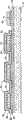
图6-图13是沿图13中的线13-13截取的横向剖面图,其中示出了用来制造图2和图3中所示的打印头的工艺的一个实施例。6-13 are transverse cross-sectional views taken along line 13-13 in FIG. 13 illustrating one embodiment of a process for manufacturing the printhead shown in FIGS. 2 and 3 .
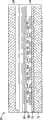
图14是沿图3中的线14-14截取的纵向剖面图的实施列。FIG. 14 is an example of a longitudinal cross-sectional view taken along line 14-14 in FIG. 3 .
图15是一个俯视图,其中示出了可以在图1中所示的打印机的打印头阵列中使用的喷墨打印头的一个实施例。Figure 15 is a top view showing one embodiment of an inkjet printhead that may be used in the printhead array of the printer shown in Figure 1 .
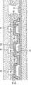
图16-图21是沿图15中的线21-21截取的纵向剖面图,其中示出了用于制造图15中所示的打印头的工艺的一个实施例。16-21 are longitudinal cross-sectional views taken along line 21 - 21 in FIG. 15 illustrating one embodiment of a process for manufacturing the printhead shown in FIG. 15 .
图22是沿图15中的线22-22截取的横向剖面图的实施例。22 is an embodiment of a transverse cross-sectional view taken along line 22-22 in FIG. 15 .
具体实施方式Detailed ways
在使用标准的半导体晶片加工工具和技术来生产适于大幅面喷墨打印应用的喷墨打印头致动器的努力中,研发出了新的静电致动器与制造工艺的实施例。因此,将参照喷墨打印来描述一些新致动器的实施例。但是,本公开的实施例并不仅限于喷墨打印。可以制造和实施其它的形式、细节和实施例。因此,不应将下文的描述理解为限制本公开的范围,本公开的范围由所附权利要求限定。In an effort to produce inkjet printhead actuators suitable for large format inkjet printing applications using standard semiconductor wafer processing tools and techniques, embodiments of new electrostatic actuators and fabrication processes were developed. Accordingly, some new actuator embodiments will be described with reference to inkjet printing. However, embodiments of the present disclosure are not limited to inkjet printing. Other forms, details and embodiments may be manufactured and implemented. Accordingly, the following description should not be taken as limiting the scope of the disclosure, which is defined by the appended claims.
图1是示出了喷墨打印机10的框图,喷墨打印机10包括:打印头14的阵列12,墨液供应部16,打印介质传送机构18和打印机电子控制器20。图1中的打印头阵列12通常表示用来将墨滴喷射到一片或者一条打印介质22上的多个打印头14以及相关的机械部件与电部件。静电喷墨打印头14可包括一个或者多个墨液喷射开口,墨液喷射开口中的每一个都与对应的墨液通道相关联。由打印头中的导体产生的静电力使墨液通道的一个壁快速地来回挠曲,以便使墨液通道交替地扩张或者收缩,从而通过对应的开口来喷射墨滴。(墨液喷射开口通常也被称作喷墨喷嘴。)在操作中,打印机控制器20以适当的顺序选择性地使一个打印头或者一组打印头中的导体通电,从而将墨液以与期望的打印图像对应的图案喷射到介质22上。1 is a block diagram illustrating an inkjet printer 10 including an
打印头阵列12和墨液供应部16可以被容纳在一起作为单个单元,或者也可以包括单独的单元。打印头阵列12可以是跨越打印介质22宽度的较大的固定单元(带墨液供应部16或者不带墨液供应部16)。可替代地,打印头阵列12可以是较小的单元,其在可移动的托架上跨越介质22的宽度来回扫描。介质传送器18使打印介质22在纵向方向上前行通过打印头阵列12。对于固定的打印头阵列12,介质传送器18可以使介质连续地前行通过阵列12。对于扫描打印头阵列12,介质传送器18可以使介质22渐进地前行通过阵列12,在打印每一行(swath)时停止,然后使介质22前行以打印下一行。控制器20可以接收来自计算机或者其它主机装置23的打印数据,如果需要,则将那些数据处理成打印机控制信息和图像数据。如果存在托架运动,则控制器20控制托架的运动,并且控制介质传送器18的运动。如上所述,控制器20被电连接到打印头阵列12,以给导体通电从而将墨滴喷射在介质22上。通过通过协调阵列12和介质22之间的相对位置,随着墨滴的喷射,控制器20根据从主机装置23接收的打印数据在介质22上产生期望的图像。
图2-图3分别是示出了打印头24的一个示例性实施例的透视图和俯视图,例如,该打印头的示例性实施例可以用作图1中所示的打印机10中的阵列12中的打印头14。大幅面喷墨打印机中的打印头阵列可以包含成百上千个单独的打印头24。参见图2和图3,打印头24是由固定到致动器芯片(die)28的墨液通道结构26组成的组件。墨液通道结构26和致动器芯片28是分开制造的,然后结合在一起,或者以其它方式彼此固定到一起,以便形成打印头24。在所示的实施例中,结构26中形成有三个墨液通道30。墨液通道30凹入到结构26的表面32中,或者以其它方式沿着结构26的表面32露出。每个墨液通道30都包括通过狭窄部38连接到前喷射室36的后填充室34,狭窄部38限定两个室34和36之间的过渡部分。墨液喷射开口40(也称作喷嘴)位于每个喷射室36的前端,如图3所示。在下面详细描述的实施例中,每个墨液通道30的一部分喷射室36也形成在致动器芯片28中。尽管希望使用传统的硅晶片加工技术(例如,光刻、蚀刻和芯片切割)在硅衬底中典型地形成墨液通道结构26,但也可以使用其它制造材料和技术。例如,只要塑料可以牢固地固定到致动器芯片28,则结构26可以通过塑模或者机加工成期望的结构配置来形成。2-3 are perspective and top views, respectively, illustrating an exemplary embodiment of a
致动器芯片28包括与每个墨液喷射室36相邻的静电致动器42。每个致动器42包括控制导体44(图3),电接触垫46和信号轨迹/布线48。下面将详细描述致动器42的这些部件以及其它部件。在填充室34处进入每个通道30的墨液通过狭窄部38进入喷射室36中,在对应的致动器42的驱使下,该墨液从喷射室36通过开口40被喷出。用于墨液通道结构26与致动器芯片28的其它配置也是可行的。例如,取决于单个打印头的性能标准、打印头阵列与打印机的特性、以及制造工具和处理技术,打印头24中的墨液通道30以及对应的致动器42的数量和形状可以由所示出的情况加以改变。The
图4A和图4B是沿着喷射室36的简化的剖面图,其中显示了致动器芯片28的操作部件。为了更好地示出每个致动器42的操作特征,从图4A和图4B中省去了芯片28和制动器42的一些结构特征。图4A显示了处于挠曲位置中的致动器42,墨液喷射室36在该挠曲位置中是扩大的。图4B显示了处于未挠曲位置中的致动器42,墨液喷射室36在该未挠曲位置中是收缩的,以便喷射墨滴。致动器42使用了被集成到致动器芯片28中的MEMS(微型机电系统)电容器。该电容器上的一个导体被附接到墨液通道30的可挠曲的膜/壁,其它/相对的导体被附接到刚性衬底,或者就是刚性衬底的一部分。施加在导体上的变化的电压信号交替地将膜拉向导体衬底以及释放该膜以便使其挠回到原始位置,从而泵送墨液通过开口40喷出。4A and 4B are simplified cross-sectional views along
参见图4A和图4B,致动器42包括沿致动器芯片的衬底52的第一非可挠导体50以及可操作地连接到墨液通道喷射室36的可挠壁56的第二可绕导体54。可挠壁56有时也被称作膜或者振动板。导体54“可操作地连接到”壁56的意思是导体54被固定或者以其它方式被约束,从而使导体54中的变形能在壁56中产生对应的变形。导体50和54在间隙58两边彼此相对地沿喷射室36延伸。非可挠导体50本身可以是可挠或者非可挠的。如果导体50是可挠的,则它会被固定到衬底52或者另一合适的衬底支撑件,以便实现所需刚度。可挠壁56的范围和/或导体54覆盖壁56的范围可以根据室36的特性而不同。不过通常希望可挠壁56能大致延伸到喷射室36的全长,并大致跨越喷射室36的整个宽度,并且还通常希望导体54大致覆盖壁56的所有可挠部分。4A and 4B, the
每个导体50和54都连接到信号发生器或者其它适当的电压源60和62,正如信号线64和66所指示的那样。在位于间隙58两端的两个导体50和54之间生成电压差,会产生能够用来使导体54以及对应的壁56来回挠曲从而使喷射室36交替地扩张和收缩的静电力。以所需方式改变电压差就能够控制墨滴通过开口40的喷射。可以使用任何适当的驱动电路和控制系统来产生所需的力。图中所示的可以通过分开的信号发生器60和62将变化的电源施加到每个导体50和54的驱动电路只是一个示例性配置。其它的配置也是可行的。例如,可以将导体50或54中的一个(通常是可挠导体54)保持在地电压,而将变化的电压施加到另一“控制”导体50或54(通常是非可挠导体50),以便获得所需的力。因此,在本文中使用的表述“导体‘可操作地连接到’电压源”的意思是以在这些导体之间产生电压差的方式连接,具体包括但不限于如上所述的连接。Each
图5是表示了沿喷射室36剖面的简化图,其中显示了静电致动器42的另一实施例的可操作部件。在图5所示的实施例中,多个控制用非可挠导体50a-50i被用来在墨液喷射室36的可挠壁56中生成波。在图5所示的实施例中,墨滴通过连续的脉冲波通过开口40喷出,而不是像图4A和图4B中所示的单个导体的实施例中那样通过一系列离散递增的波从而喷出。所产生的蠕动式泵送可以用来控制开口40处的弯液面,并且帮助减少:(1)通过开口40摄取的气泡和/或(2)从开口40中淌出的墨液或其它液体。如本文中所使用的那样,蠕动式泵送的意思是通过收缩和/或扩张的波来使流体运动。在图5中通过时间线t1-t7示出一个示例性的电压/信号脉冲的行进。在该示例性的行进中,可挠导体54被保持在地电压,而信号发生器60以预定脉冲波形通过例如一系列门或者开关68a-68i同时给四个导体施加脉冲,随着每一次的时间递增,该脉冲波形移动通过一个导体。在时间t1,脉冲被施加到导体50d/50e和50h/50i;在时间t2,脉冲被施加到导体50c/50d和50g/50h;如此类推。图5中所示的开关68a-68i的状态对应于在时间t7所示的脉冲波形。可以如所需地设定和/或改变该脉冲波形和行进,以便实现墨滴通过开口40的正确流动。FIG. 5 is a simplified diagram showing a cross-section through
现在参照图6-图14描述致动器芯片28的结构的一个实施例和用于制造芯片28和打印头24的一个示例性工艺。图13是示出了沿显示打印头24的图3中的线13-13所剖取的横向剖视图。图14是示出了沿显示打印头24的图3中的线14-14所剖取的纵向剖面图。图6-图12是显示制造致动器芯片28和打印头24的工艺步骤的横向剖面图。图6-图14中所示的结构不是按比例绘制的,并且与图3中所示的对应结构也不是准确关联的。相反,图6-图14中所示的结构是以图示的方式展现的,以便帮助显示本公开的该实施例的相关结构和加工特征。One embodiment of the structure of the
首先参照图6,通过例如热氧化衬底72的表面以便形成二氧化硅层,从而在硅衬底72上形成薄的氧化层70。氧化层70充当后续间隔件蚀刻的硬掩模,并且提供良好的结合面。因此,尽管在许多应用中期望使用氧化层,但其它的配置也是可行的。例如,在间隔件蚀刻中使用光致抗蚀剂的情况下,未被氧化的硅衬底72可以提供可接受的结合面。此外,尽管示出了单个致动器芯片的部件的形成,但可以在硅晶片(衬底72)上同时形成许多个这样的芯片的部件,随后将各个芯片从晶片上切割出来,或者以其它方式从晶片上分离。同样,尽管是按照金属氧化物半导体(MOS)技术(金属氧化物半导体技术是最常用的集成电路技术中的一种)描述本公开的,但可以使用其它适当的技术。在薄的氧化物70上沉积或者以其它方式形成一层铝化钽(TaAl)或者另一适当的导电材料。通过例如图案化并蚀刻导电层来选择性地去除导电层,以便形成控制导体74和接触垫76(图3中的导体44和接触垫46)。Referring first to FIG. 6, a
集成电路的形成通常包括光刻掩膜和蚀刻。该工艺包括:产生包含有待形成的部件的图案的光刻掩膜;用被称作光致抗蚀剂的光敏材料涂覆晶片;将涂覆有光致抗蚀剂的晶片暴露给紫外光,通过掩膜的紫外光根据所使用的是正的光致抗蚀剂或者负的光致抗蚀剂来软化或硬化光致抗蚀剂部分;去除光致抗蚀剂的软化部分;进行蚀刻以去除未受光致抗蚀剂保护的材料;剥离剩余的光致抗蚀剂。该光刻掩膜和蚀刻工艺在本文中被称作“图案化及蚀刻”。尽管希望通过图案化及蚀刻来达到选择性去除材料的目的,但可以使用其它的选择性去除工艺。因此,对所描述并示出的示例性的制造工艺中提到图案化及蚀刻的参考不应被理解为是对附于说明书之后的权利要求中所述的选择性去除材料中可以使用的工艺的限制。Formation of integrated circuits typically involves photolithographic masking and etching. The process involves: creating a photolithographic mask that contains the pattern of the features to be formed; coating the wafer with a light-sensitive material called photoresist; exposing the photoresist-coated wafer to ultraviolet light, UV light through the mask softens or hardens portions of the photoresist depending on whether a positive or negative photoresist is used; removes the softened portion of the photoresist; etches to remove Material not protected by photoresist; strip remaining photoresist. This photolithographic masking and etching process is referred to herein as "patterning and etching." Although patterning and etching are desired for selective removal of material, other selective removal processes may be used. Accordingly, references to patterning and etching in the described and illustrated exemplary fabrication processes should not be understood as processes that may be used in the selective removal of material as described in the claims appended hereto limits.
参照图7,在导体74之上形成牺牲间隔件78。间隔件78稍后被移除从而限定可挠打印头导体和非可挠打印头导体之间(即,电容器导体之间)的静电间隙。每个间隔件78可以构成非晶硅或者其它适当材料的单体,其沉积在下层结构上,然后被图案化并蚀刻成所需形状。可替代地,间隔件78可以构成不止一层材料的复合物。例如,可以首先在下层结构上沉积一层厚度大约为导体74的厚度的非晶硅来形成间隔件78。该第一硅层通过例如化学机械抛光来被平坦化至导体74所在处。如必需或者需要,则该平坦化过程还可以延伸到导体74,以便帮助确保用于进一步加工以及用于均匀的静电间隙的平坦表面。然后在下层结构上形成薄的氮化硅层,在氮化硅上沉积厚的非晶硅层。硅/氮化物/硅的叠层被图案化并被蚀刻以便形成多个间隔件78,每个间隔件78都包括夹在硅侧壁80和硅盖84之间的薄的氮化硅层82。虽然可以使用任何适当的间隔件材料,但需要使用相对导体74和氧化物70可选择性蚀刻的材料,以便帮助控制间隔件释放蚀刻,这将在下文描述。Referring to FIG. 7 ,
现在参照图8,在所示的实施例中,沿每个墨液通道的壁的可挠部86构成夹在绝缘层88和92之间的导电层90。在本文中,可挠壁部86有时也被称作膜86。在下层结构上形成有薄的绝缘层88,在绝缘层88上沉积铝化钽(TaAl)层90或者另一适当的导体,在导体层90上形成第二薄的绝缘层92。尽管希望通过使用正硅酸乙酯低温化学汽相沉积(TEOS)工艺沉积二氧化硅来形成绝缘层88和92,但也可以使用其它适当的材料和工艺。绝缘的导体叠层94被图案化并被蚀刻以形成膜86,并露出接触垫76。与留下部分牺牲间隔件以便分隔控制导体的传统的静电打印头不同,叠层94用来在横向方向(图8-图13)和纵向方向(图14)上都将控制导体74彼此分开,从而允许在释放蚀刻中完全移除间隔件78。在释放蚀刻之后,掉落在控制导体74之间的衬底(在氧化层70处)的那部分叠层94也支撑膜86(叠层94的水平可挠部分)。因此,用于打印头24中的膜层的该配置相比传统的打印头具有两个显著的优点。首先,膜层是自支撑的;其次,膜层可以用来分隔控制导体。Referring now to FIG. 8 , in the illustrated embodiment, the
参照图9,在绝缘的导体叠层94上形成第二牺牲间隔件96。间隔件96稍后被去除以限定膜86的宽度。每个间隔件96都可构造成沉积在下层结构上的非晶硅或者其它适当材料的单体,然后被图案化并被蚀刻成所需形状。同样,虽然可以使用任何适当的间隔件材料,但期望使用相对于氧化层92可选择性蚀刻的材料,以便帮助控制释放蚀刻。Referring to FIG. 9 , a second
参照图10,在下层结构上形成厚的TEOS氧化物层或者其它适当的绝缘层98。通过例如化学机械抛光,绝缘层98被平坦化以提供用于将致动器芯片28结合到墨液通道结构26的平坦光滑表面。绝缘层98被图案化并被蚀刻以露出牺牲间隔件96,并部分形成延伸到致动器芯片28中的墨液通道延伸部分。如图11中所示,该蚀刻可以继续,以便露出接触垫76并且打开孔100以便露出牺牲间隔件78。可替代地,第二掩膜/图案化及蚀刻步骤可以用来露出接触垫76,并打开孔100以便露出牺牲间隔件78。然后进行被称作“释放”的蚀刻,以便去除间隔件96和78,形成图11中所示的结构。TEOS层92和98,氧化层88和金属控制导体74用作蚀刻阻挡部,而正在蚀刻的硅间隔件78和96帮助在不破坏周围结构的情况下完全去除间隔件78和96。也就是说,释放蚀刻是选择性去除非晶硅间隔件材料,但却不会去除氧化物和金属。因此,释放蚀刻的定时对于限定通过去除间隔件78所形成的静电间隙58或者通过去除间隔件96所限定的致动器宽度不再非常重要。Referring to FIG. 10, a thick TEOS oxide layer or other suitable insulating
面向控制导体74的绝缘层88提供了导体74和90之间的电绝缘,并且帮助防止该导体之间的短路。面向墨液通道30的绝缘层92隔离导体90使其免受墨液的化学侵袭。然而,取决于打印头24中许多设计因素的选择,具体包括导电膜86的静电位移,间隙58的大小,以及静摩擦凸块或者其它防止短路的结构的使用,可以省去绝缘层88。类似地,如果导电层90不容易因打印头24中使用的墨液而造成化学退化,则可以省去绝缘层92。因此,可以由不绝缘的导电层90形成膜86,该导电层90是抗墨液侵蚀的,并且还另外被配置成不与控制导体74短路。
通过等离子结合或者另外的适当的结合工艺,墨液通道结构26被结合到已形成的致动器芯片28(如图12所示),以将每个墨液通道30与对应的膜86配合,并且覆盖通孔100。然后,通过例如锯切割来去除墨液通道结构26位于接触垫76(图2和图3中是垫46)上的那部分,以露出垫76。The
在图13和图14(图14是沿图3中的线14-14剖取的纵向剖视图)中示出了已形成的打印头24。上述的各层和各部件的具体尺寸根据打印应用可以有很大的变化。不过,对于非常大幅的打印应用(其中一个阵列包括了数百个打印头)的阵列12(图1)所使用的静电喷墨打印头24而言,下面是打印分辨率为600dpi(点/英寸)的打印头24中一些组件的正常尺寸的一个例子。每个墨液通道30和对应的膜86大约为30微米宽。静电间隙58和膜86的厚度分别为大约200纳米(导体90的厚度大约为100纳米,每个TEOS氧化物层的厚度大约为50纳米)。每个墨液通道30中的喷射室36的深度(包括形成在结构26和芯片28中的部分)大约为100微米。The formed
现在参照图15-22描述致动器芯片28结构的另一实施例,以及用于制造芯片28和打印头24的另一示例性工艺。图21是纵向剖视图,其中示出了沿显示打印头24的图15中的线21-21剖取的视图。图22是横向剖视图,其中示出了沿显示打印头24的图15中的线22-22剖取的视图。图16-图20是显示了制造致动器芯片28和打印头24的工艺步骤的纵向剖视图。如下面将详细描述那样,在该实施例中,在控制电极之间形成静摩擦凸块,并且膜层仅在横向方向上掉落到控制电极之间的衬底上。图16-图22中所示的结构不是按比例绘制的,并且它们与图15中所示的对应结构也不是准确关联的。相反,图16-图22中所示的结构是以图示方式呈现的,以便帮助显示本公开的该实施例的相关结构和加工特征。Another embodiment of an
首先参照图15,在致动器芯片28中沿着每个通道30的长度位于控制电极44之间形成所谓的“静摩擦”凸块102。静摩擦凸块用在MEMS器件中以便帮助降低不需要的粘附(STIcking)和摩擦(friCTION)(因此,称作“静摩擦(stiction)”),和/或提供将导体物理隔离从而帮助防止导体之间电短路的机械防护件(stand-off)。本文中使用的“静摩擦凸块”是指被配置成执行这些功能中的任意一种或全部两种的凸块。图15中所示的其它部件与图3显示和描述的那些部件相同。打印头24是由固定到致动器芯片28的墨液通道结构26组成的组件。墨液通道结构26和致动器芯片28是分开制造的,然后再结合在一起或者以其它方式相互固定,以便形成打印头24。每个墨液通道30都包括通过狭窄部38连接到前喷射室36的后填充室34,狭窄部38限定两个室34和36之间的过渡部分。墨液喷射开口40(也称作喷嘴)位于每个喷射室36的前端。致动器芯片28包括邻近每个墨液喷射室36的静电致动器42。每个致动器42都包括控制导体44、电接触垫46和信号轨迹/布线48。Referring first to FIG. 15 , so-called "stiction" bumps 102 are formed in the
现在参见图16,在硅衬底72上通过例如热氧化衬底72的表面以形成二氧化硅层的方式形成薄的氧化层70。氧化层70充当硬掩膜,以便用于后续的间隔件蚀刻,并且氧化层70还提供了良好的结合面。因此,尽管在许多应用中期望使用氧化物层,但是其它的配置也是可行的。例如,未被氧化的硅衬底72可以提供可接受的结合面,在这种情况下可以将光致抗蚀剂用于间隔件蚀刻。在薄的氧化物70上沉积或者以其它方式形成一层铝化钽(TaAl)或者另一适当的导电材料。通过例如图案化和蚀刻该导电层,选择性地去除导电层,从而形成控制导体74(图15中的导体44)和静摩擦凸挡块104。尽管预期同时以相同的材料形成凸挡块104和控制导体74是方便的,但也可以分别形成控制导体74和凸挡块104,而且凸挡块还可以由包括绝缘材料的另一材料形成。Referring now to FIG. 16, a
参照图17,在导体74之上形成牺牲间隔件78。间隔件78稍后被移除,以便限定位于可挠打印头导体与非可挠打印头导体之间(即,电容导体之间)的静电间隙。在所示的实施例中,间隔件78包括夹在硅侧壁80和硅盖84之间的薄的氮化硅层82。尽管可以使用任何适当的间隔件材料,但希望使用对于导体74和氧化物70可选择性地蚀刻的材料,以便帮助控制下文将描述的间隔件释放蚀刻。在每个凸挡块104之上的静摩擦凸块102的期望位置处,在间隔件78的上表面(硅盖84)中蚀刻或者以其它方式形成凹陷部106。Referring to FIG. 17 ,
参照图18,在此实施例中,导电膜86是由单个导体层90构成的。导电层90被图案化以及被蚀刻,以形成膜86并露出接触垫46(参见图22)。填充每个凹陷部106的导电层90形成静摩擦凸块102。同样在该实施例中,导体层90只在横向方向上将控制导体44彼此隔开,这通过比较图21和图22可清楚看出。在释放蚀刻之后,导体90落在图22中控制导体74/44之间的衬底(氧化层70)上的那部分(导体90的水平、可挠部分)也支撑膜86。Referring to FIG. 18 , in this embodiment, the
参照图19,在导体90上形成第二牺牲间隔件96。间隔件96稍后被去除以限定膜86的宽度(参见图22)。然后,在下层结构上形成厚的TEOS氧化物层或者其它适当的绝缘层98。绝缘层98通过例如化学机械抛光被平坦化,以提供用于将致动器芯片28结合到墨液通道结构26的平坦光滑表面。绝缘层98被图案化并蚀刻以露出牺牲间隔件96,并部分地形成油墨通道延伸到致动器芯片28中的延伸部,如上述参照图10和图11描述的那样。如图22中所示,该蚀刻可以继续,以露出接触垫46,并打开孔100,从而露出牺牲间隔件78。可替代地,可以用第二掩模/图案化及蚀刻步骤来露出接触垫76,并打开通孔100。Referring to FIG. 19 , a second
然后执行释放蚀刻,以去除间隔件96和78,形成图20中所示的结构。通过等离子结合或者另外的适当的结合工艺,墨液通道结构26被结合至已形成的致动器芯片28,如图21和图22中所示那样,以将每个墨液通道30与对应的膜86配合,并覆盖通通孔100。然后,通过例如用锯切割来去除墨液通道结构26在接触垫76(在图2-3和图22中是垫46)之上的这部分,以露出垫76。参照图21,当膜86朝向导体44向下挠曲时,静摩擦凸块102提供了使导电膜86和控制导体44物理隔开的机械防护,以便帮助防止导体86和44之间的电短路。在凸挡块104也导电的情况下,挡块104和凸块102保持以相同的电压,从而使得导体102和104也彼此短路。A release etch is then performed to remove
在一个实施例中,喷墨打印头包括:In one embodiment, the inkjet printhead comprises:
第一结构,其具有形成于该第一结构的结合面上的多个第一墨液通道,第一墨液通道布置成大致彼此平行地穿过第一结构的结合面;a first structure having a plurality of first ink channels formed on the bonding surface of the first structure, the first ink channels being arranged substantially parallel to each other across the bonding surface of the first structure;
第二结构,其具有形成于该第二结构的结合面上的多个第二墨液通道,第二墨液通道布置成大致彼此平行地穿过第二结构的结合面,第一结构和第二结构以其各自的结合面彼此结合,使得每个第一墨液通道与对应的一个第二墨液通道对齐,从而形成多个墨液室,第二结构包括静电致动器,该静电致动器包括:A second structure having a plurality of second ink channels formed on a joint face of the second structure, the second ink channels being arranged substantially parallel to each other across the joint face of the second structure, the first structure and the first structure The two structures are combined with each other with their respective joint surfaces, so that each first ink channel is aligned with a corresponding second ink channel, thereby forming a plurality of ink chambers. The second structure includes an electrostatic actuator. Actuators include:
具有多个可挠第一部的第一导体,该多个可挠第一部由多个第二部支撑,每个可挠第一部至少限定每个第二墨液通道的一个壁的一部分;以及A first conductor having a plurality of flexible first portions supported by a plurality of second portions, each flexible first portion defining at least a portion of one wall of each second ink channel ;as well as
多个第二导体,每个第二导体在间隙另一边与相对的第一导体的第一部中对应的一个对齐;以及a plurality of second conductors, each second conductor being aligned with a corresponding one of the first portions of the opposing first conductors on the other side of the gap; and
每个油墨室中的开口,在致动器作用下流体可以通过该开口从室中喷出。An opening in each ink chamber through which fluid may be ejected from the chamber upon action of the actuator.
在该喷墨打印头的实施例中,第二导体的第二部可以设置在定位成彼此邻近的每对第一导体之间。在该喷墨打印头的实施例中,致动器可以进一步包括可操作地连接到每个第二导体的电压源,用于选择性地在第二导体中的每一个和第一导体之间施加电压。In an embodiment of the inkjet printhead, the second portion of the second conductor may be disposed between each pair of first conductors positioned adjacent to each other. In an embodiment of the inkjet printhead, the actuator may further comprise a voltage source operably connected to each second conductor for selectively switching between each of the second conductors and the first conductor Apply voltage.
在一个实施例中,喷墨打印机包括:In one embodiment, an inkjet printer includes:
墨液供应部;ink supply department;
可操作地连接到墨液供应部的打印头阵列,阵列中的每个打印头都包括静电致动器,用于从该打印头中的多个墨液室中喷射墨滴,该致动器包括:An array of printheads operatively connected to an ink supply, each printhead in the array including an electrostatic actuator for ejecting ink drops from a plurality of ink chambers in the printhead, the actuator include:
多个第一导体,每个第一导体都与一个墨液室关联;a plurality of first conductors, each associated with an ink chamber;
绝缘的第二导体,其具有多个可挠第一部和多个第二部,每个可挠第一部至少形成室壁的一部分,每个可挠第一部位于间隙另一边与对应的一个第一导体相对;每个第二部将一个第一导体与另一个第一导体隔开;以及An insulated second conductor having a plurality of flexible first portions and a plurality of second portions, each flexible first portion forming at least a portion of a chamber wall, each flexible first portion located on the other side of the gap with a corresponding one first conductor is opposite; each second portion separates one first conductor from the other first conductor; and
可操作地连接到每个第二导体的电压源,用于选择性地在第二导体中的每一个和第一导体之间施加电压;a voltage source operably connected to each second conductor for selectively applying a voltage between each of the second conductors and the first conductor;
可操作地连接到打印头的电子控制器,用于选择性地启动打印头中的静电致动器;以及an electronic controller operatively connected to the printhead for selectively activating the electrostatic actuator in the printhead; and
打印介质传送机构,其被配置成在控制器起作用时,使打印介质移动通过打印头阵列。A print media transport mechanism configured to, upon activation of the controller, move print media through the printhead array.
在一个实施例中,一种形成静电致动器的方法包括:In one embodiment, a method of forming an electrostatic actuator includes:
在一结构上以及在第一导体上形成第一间隔件材料层;forming a first layer of spacer material on a structure and on the first conductor;
选择性地去除第一间隔件材料层的一部分,以形成覆盖每个第一导体的第一间隔件,并露出第一间隔件之间的结构;selectively removing a portion of the layer of first spacer material to form a first spacer overlying each of the first conductors and exposing structures between the first spacers;
用绝缘的第二导体覆盖第一间隔件和第一间隔件之间露出的结构;covering the first spacer and the exposed structure between the first spacer with an insulated second conductor;
在绝缘的第二导体上形成第二间隔件材料层;forming a second layer of spacer material on the insulated second conductor;
选择性地去除第二间隔件材料层的一部分,以在绝缘的第二导体上形成第二间隔件,该绝缘的第二导体直接位于每个第一导体之上;selectively removing a portion of the layer of second spacer material to form a second spacer on the insulated second conductors directly above each of the first conductors;
用绝缘材料覆盖第二间隔件和绝缘的导体;covering the second spacer and the insulated conductor with insulating material;
选择性地去除该绝缘材料的一部分,从而在绝缘材料中暴露出沿着通道的第二间隔件;以及selectively removing a portion of the insulating material, thereby exposing a second spacer along the channel in the insulating material; and
去除第一间隔件和第二间隔件。Remove the first spacer and the second spacer.
在该形成实施例的方法中,所述结构可以包括硅结构,并且用第二导体覆盖第一间隔件和第一间隔件之间露出的结构可以包括用绝缘的第二导体覆盖第一间隔件和第一间隔件之间露出的结构。In the method of forming an embodiment, the structure may include a silicon structure, and covering the first spacer and the structure exposed between the first spacer with a second conductor may include covering the first spacer with an insulated second conductor and the structure exposed between the first spacer.
如在本说明书的开始部分所述的那样,在附图中示出并在上文描述的示例性实施例是对要求保护的主题的说明,而并非是限制。可以制造并实施其它的形式、细节和实施例。因此,不应将上述描述理解为是对要求保护的主题的范围的限制,该范围在所附权利要求中进行限定。As stated in the opening part of this specification, the exemplary embodiments shown in the drawings and described above are illustrative of the claimed subject matter and not limiting. Other forms, details and embodiments may be manufactured and implemented. Accordingly, the foregoing description should not be taken as limiting the scope of the claimed subject matter, which is defined in the appended claims.
Claims (15)
Applications Claiming Priority (4)
| Application Number | Priority Date | Filing Date | Title |
|---|---|---|---|
| US11/831,542 | 2007-07-31 | ||
| US11/831542 | 2007-07-31 | ||
| US11/831,542US7625075B2 (en) | 2007-07-31 | 2007-07-31 | Actuator |
| PCT/US2008/071540WO2009018308A1 (en) | 2007-07-31 | 2008-07-30 | Actuator |
Publications (2)
| Publication Number | Publication Date |
|---|---|
| CN101784390Atrue CN101784390A (en) | 2010-07-21 |
| CN101784390B CN101784390B (en) | 2013-06-19 |
Family
ID=40304828
Family Applications (1)
| Application Number | Title | Priority Date | Filing Date |
|---|---|---|---|
| CN2008801014108AExpired - Fee RelatedCN101784390B (en) | 2007-07-31 | 2008-07-30 | Actuator and injector including actuator |
Country Status (5)
| Country | Link |
|---|---|
| US (1) | US7625075B2 (en) |
| EP (2) | EP2173559B1 (en) |
| CN (1) | CN101784390B (en) |
| TW (1) | TWI450827B (en) |
| WO (1) | WO2009018308A1 (en) |
Cited By (2)
| Publication number | Priority date | Publication date | Assignee | Title |
|---|---|---|---|---|
| CN105984217A (en)* | 2015-03-19 | 2016-10-05 | 施乐公司 | Membrane bond alignment for electrostatic ink jet printhead |
| CN109313117A (en)* | 2016-07-26 | 2019-02-05 | 惠普发展公司,有限责任合伙企业 | Microfluidic device |
Families Citing this family (8)
| Publication number | Priority date | Publication date | Assignee | Title |
|---|---|---|---|---|
| JP5355223B2 (en)* | 2008-06-17 | 2013-11-27 | キヤノン株式会社 | Liquid discharge head |
| US8952463B2 (en)* | 2008-07-08 | 2015-02-10 | Pixart Imaging Incorporation | MEMS structure preventing stiction |
| US8389084B2 (en)* | 2009-02-27 | 2013-03-05 | Fujifilm Corporation | Device with protective layer |
| JP5768393B2 (en)* | 2011-02-10 | 2015-08-26 | 株式会社リコー | Ink jet head and image forming apparatus |
| US9193161B2 (en)* | 2012-04-19 | 2015-11-24 | Hewlett-Packard Development Company, L.P. | Fluid circulation within chamber |
| US20230068297A1 (en)* | 2020-01-29 | 2023-03-02 | Hewlett-Packard Development Company, L.P. | Determining flow rates with thermal sensors |
| CN113285012A (en)* | 2020-02-20 | 2021-08-20 | 丰田自动车株式会社 | Actuator and method for manufacturing actuator |
| EP4590625A1 (en)* | 2022-09-22 | 2025-07-30 | Hewlett-Packard Development Company, L.P. | Plasma bonding formation of direct electrical and fluidic interconnects |
Family Cites Families (21)
| Publication number | Priority date | Publication date | Assignee | Title |
|---|---|---|---|---|
| US6120124A (en)* | 1990-09-21 | 2000-09-19 | Seiko Epson Corporation | Ink jet head having plural electrodes opposing an electrostatically deformable diaphragm |
| JPH1016208A (en)* | 1996-06-28 | 1998-01-20 | Seiko Instr Inc | Droplet emitting method, droplet emitting head and ink emitting head |
| JP3760625B2 (en) | 1998-03-06 | 2006-03-29 | コニカミノルタホールディングス株式会社 | Inkjet head |
| US6322198B1 (en)* | 1998-04-07 | 2001-11-27 | Minolta Co., Ltd. | Electrostatic inkjet head having spaced electrodes |
| US6491378B2 (en)* | 1998-12-08 | 2002-12-10 | Seiko Epson Corporation | Ink jet head, ink jet printer, and its driving method |
| JP2001113701A (en)* | 1999-08-06 | 2001-04-24 | Ricoh Co Ltd | Electrostatic inkjet head and method of manufacturing the same |
| EP1075949B8 (en) | 1999-08-09 | 2006-12-20 | Seiko Epson Corporation | Driving method and driving device for an inkjet head |
| JP3716724B2 (en) | 1999-09-30 | 2005-11-16 | ブラザー工業株式会社 | Piezoelectric actuator for piezoelectric ink jet printer head and method for manufacturing the same |
| US6508947B2 (en)* | 2001-01-24 | 2003-01-21 | Xerox Corporation | Method for fabricating a micro-electro-mechanical fluid ejector |
| JP3809787B2 (en) | 2001-06-26 | 2006-08-16 | ブラザー工業株式会社 | Inkjet printer head |
| JP2005238540A (en)* | 2004-02-25 | 2005-09-08 | Sony Corp | Fluid driving device, manufacturing method for fluid driving device, electrostatically driven fluid discharging apparatus, and manufacturing method for electrostatically driven fluid discharging apparatus |
| JP2005262686A (en) | 2004-03-18 | 2005-09-29 | Ricoh Co Ltd | Actuator, droplet discharge head, ink cartridge, ink jet recording apparatus, micro pump, light modulation device, substrate |
| US7334871B2 (en)* | 2004-03-26 | 2008-02-26 | Hewlett-Packard Development Company, L.P. | Fluid-ejection device and methods of forming same |
| JP4569151B2 (en)* | 2004-03-31 | 2010-10-27 | ブラザー工業株式会社 | Inkjet printer head unit, inkjet printer, and signal transmission board used therefor |
| JP2006007560A (en)* | 2004-06-25 | 2006-01-12 | Sony Corp | Functional element, its manufacturing method, fluid discharging apparatus, and printer |
| JP2006035571A (en) | 2004-07-26 | 2006-02-09 | Brother Ind Ltd | Inkjet head |
| JP4609014B2 (en)* | 2004-09-17 | 2011-01-12 | ブラザー工業株式会社 | Inkjet head |
| JP4583888B2 (en)* | 2004-11-11 | 2010-11-17 | 株式会社リコー | Droplet discharge head, head driving device, liquid cartridge, and image forming apparatus |
| US7226146B2 (en)* | 2004-11-30 | 2007-06-05 | Xerox Corporation | Fluid ejection devices and methods for forming such devices |
| US7267043B2 (en)* | 2004-12-30 | 2007-09-11 | Adaptivenergy, Llc | Actuators with diaphragm and methods of operating same |
| JP4424331B2 (en)* | 2005-08-01 | 2010-03-03 | セイコーエプソン株式会社 | Electrostatic actuator, droplet discharge head, method for driving droplet discharge head, and method for manufacturing electrostatic actuator |
- 2007
- 2007-07-31USUS11/831,542patent/US7625075B2/enactiveActive
- 2008
- 2008-07-25TWTW097128398Apatent/TWI450827B/ennot_activeIP Right Cessation
- 2008-07-30EPEP08796829.3Apatent/EP2173559B1/ennot_activeNot-in-force
- 2008-07-30WOPCT/US2008/071540patent/WO2009018308A1/enactiveApplication Filing
- 2008-07-30EPEP19158111.5Apatent/EP3505351B1/enactiveActive
- 2008-07-30CNCN2008801014108Apatent/CN101784390B/ennot_activeExpired - Fee Related
Cited By (5)
| Publication number | Priority date | Publication date | Assignee | Title |
|---|---|---|---|---|
| CN105984217A (en)* | 2015-03-19 | 2016-10-05 | 施乐公司 | Membrane bond alignment for electrostatic ink jet printhead |
| CN105984217B (en)* | 2015-03-19 | 2019-01-01 | 施乐公司 | A kind of ink-jet printer, electrostatic inkjet print head and the method for forming the print head |
| CN109313117A (en)* | 2016-07-26 | 2019-02-05 | 惠普发展公司,有限责任合伙企业 | Microfluidic device |
| US11203017B2 (en) | 2016-07-26 | 2021-12-21 | Hewlett-Packard Development Company, L.P. | Microfluidic apparatuses |
| CN109313117B (en)* | 2016-07-26 | 2022-01-14 | 惠普发展公司,有限责任合伙企业 | Microfluidic device, method for controlling a fluid, and microfluidic system |
Also Published As
| Publication number | Publication date |
|---|---|
| EP3505351A1 (en) | 2019-07-03 |
| EP2173559A1 (en) | 2010-04-14 |
| EP3505351B1 (en) | 2021-06-02 |
| CN101784390B (en) | 2013-06-19 |
| TWI450827B (en) | 2014-09-01 |
| WO2009018308A1 (en) | 2009-02-05 |
| EP2173559A4 (en) | 2012-08-15 |
| EP2173559B1 (en) | 2019-04-03 |
| US20090033718A1 (en) | 2009-02-05 |
| TW200911542A (en) | 2009-03-16 |
| US7625075B2 (en) | 2009-12-01 |
Similar Documents
| Publication | Publication Date | Title |
|---|---|---|
| CN101784390A (en) | Actuator | |
| US6508947B2 (en) | Method for fabricating a micro-electro-mechanical fluid ejector | |
| KR100438836B1 (en) | Piezo-electric type inkjet printhead and manufacturing method threrof | |
| US6572218B2 (en) | Electrostatically-actuated device having a corrugated multi-layer membrane structure | |
| EP1681169B1 (en) | Piezoelectric inkjet printhead and method of manufacturing the same | |
| KR20070078201A (en) | Piezoelectric inkjet printheads and manufacturing method thereof | |
| CN101288864A (en) | Liquid spray head based on piezoelectric bridge type beam and flexible film | |
| JPH11207952A (en) | Ink-jet head and method for driving the same | |
| CN101293234A (en) | Liquid nozzle based on piezoelectric cantilever beam and flexible film | |
| JP2014004724A (en) | Liquid discharge head | |
| TWI436901B (en) | Electrostatic actuator and fabrication method | |
| CN101284263A (en) | Liquid spray head based on piezoelectric bridge type beam | |
| KR100528349B1 (en) | Piezo-electric type inkjet printhead and manufacturing method threrof | |
| KR100561865B1 (en) | Piezoelectric inkjet printheads and manufacturing method thereof | |
| KR100327250B1 (en) | A micro actuator of inkjet printhead and manufacturing method thereof | |
| KR100698347B1 (en) | Electrostatic Actuators Manufactured by Semiconductor Manufacturing Process | |
| US20050253908A1 (en) | Inkjet printhead with supply ducts in reverse side of water | |
| HK1072036B (en) | Electrostatic actuator formed by a semiconductor manufacturing process | |
| HK1072036A1 (en) | Electrostatic actuator formed by a semiconductor manufacturing process |
Legal Events
| Date | Code | Title | Description |
|---|---|---|---|
| C06 | Publication | ||
| PB01 | Publication | ||
| C10 | Entry into substantive examination | ||
| SE01 | Entry into force of request for substantive examination | ||
| C14 | Grant of patent or utility model | ||
| GR01 | Patent grant | ||
| CF01 | Termination of patent right due to non-payment of annual fee | Granted publication date:20130619 | |
| CF01 | Termination of patent right due to non-payment of annual fee |