CN101783449A - Electrical Connector System - Google Patents
Electrical Connector SystemDownload PDFInfo
- Publication number
- CN101783449A CN101783449ACN200911000191ACN200911000191ACN101783449ACN 101783449 ACN101783449 ACN 101783449ACN 200911000191 ACN200911000191 ACN 200911000191ACN 200911000191 ACN200911000191 ACN 200911000191ACN 101783449 ACN101783449 ACN 101783449A
- Authority
- CN
- China
- Prior art keywords
- electrical
- housing
- wafer
- ground
- electrical contact
- Prior art date
- Legal status (The legal status is an assumption and is not a legal conclusion. Google has not performed a legal analysis and makes no representation as to the accuracy of the status listed.)
- Granted
Links
Images


Classifications
- H—ELECTRICITY
- H01—ELECTRIC ELEMENTS
- H01R—ELECTRICALLY-CONDUCTIVE CONNECTIONS; STRUCTURAL ASSOCIATIONS OF A PLURALITY OF MUTUALLY-INSULATED ELECTRICAL CONNECTING ELEMENTS; COUPLING DEVICES; CURRENT COLLECTORS
- H01R13/00—Details of coupling devices of the kinds covered by groups H01R12/70 or H01R24/00 - H01R33/00
- H01R13/46—Bases; Cases
- H01R13/514—Bases; Cases composed as a modular blocks or assembly, i.e. composed of co-operating parts provided with contact members or holding contact members between them
- H—ELECTRICITY
- H01—ELECTRIC ELEMENTS
- H01R—ELECTRICALLY-CONDUCTIVE CONNECTIONS; STRUCTURAL ASSOCIATIONS OF A PLURALITY OF MUTUALLY-INSULATED ELECTRICAL CONNECTING ELEMENTS; COUPLING DEVICES; CURRENT COLLECTORS
- H01R12/00—Structural associations of a plurality of mutually-insulated electrical connecting elements, specially adapted for printed circuits, e.g. printed circuit boards [PCB], flat or ribbon cables, or like generally planar structures, e.g. terminal strips, terminal blocks; Coupling devices specially adapted for printed circuits, flat or ribbon cables, or like generally planar structures; Terminals specially adapted for contact with, or insertion into, printed circuits, flat or ribbon cables, or like generally planar structures
- H01R12/70—Coupling devices
- H01R12/71—Coupling devices for rigid printing circuits or like structures
- H01R12/72—Coupling devices for rigid printing circuits or like structures coupling with the edge of the rigid printed circuits or like structures
- H01R12/722—Coupling devices for rigid printing circuits or like structures coupling with the edge of the rigid printed circuits or like structures coupling devices mounted on the edge of the printed circuits
- H01R12/725—Coupling devices for rigid printing circuits or like structures coupling with the edge of the rigid printed circuits or like structures coupling devices mounted on the edge of the printed circuits containing contact members presenting a contact carrying strip, e.g. edge-like strip
- H—ELECTRICITY
- H01—ELECTRIC ELEMENTS
- H01R—ELECTRICALLY-CONDUCTIVE CONNECTIONS; STRUCTURAL ASSOCIATIONS OF A PLURALITY OF MUTUALLY-INSULATED ELECTRICAL CONNECTING ELEMENTS; COUPLING DEVICES; CURRENT COLLECTORS
- H01R13/00—Details of coupling devices of the kinds covered by groups H01R12/70 or H01R24/00 - H01R33/00
- H01R13/646—Details of coupling devices of the kinds covered by groups H01R12/70 or H01R24/00 - H01R33/00 specially adapted for high-frequency, e.g. structures providing an impedance match or phase match
- H01R13/6461—Means for preventing cross-talk
- H01R13/6471—Means for preventing cross-talk by special arrangement of ground and signal conductors, e.g. GSGS [Ground-Signal-Ground-Signal]
- H—ELECTRICITY
- H01—ELECTRIC ELEMENTS
- H01R—ELECTRICALLY-CONDUCTIVE CONNECTIONS; STRUCTURAL ASSOCIATIONS OF A PLURALITY OF MUTUALLY-INSULATED ELECTRICAL CONNECTING ELEMENTS; COUPLING DEVICES; CURRENT COLLECTORS
- H01R13/00—Details of coupling devices of the kinds covered by groups H01R12/70 or H01R24/00 - H01R33/00
- H01R13/648—Protective earth or shield arrangements on coupling devices, e.g. anti-static shielding
- H01R13/658—High frequency shielding arrangements, e.g. against EMI [Electro-Magnetic Interference] or EMP [Electro-Magnetic Pulse]
- H01R13/6581—Shield structure
- H01R13/6585—Shielding material individually surrounding or interposed between mutually spaced contacts
- H01R13/6586—Shielding material individually surrounding or interposed between mutually spaced contacts for separating multiple connector modules
- H01R13/6587—Shielding material individually surrounding or interposed between mutually spaced contacts for separating multiple connector modules for mounting on PCBs
Landscapes
- Details Of Connecting Devices For Male And Female Coupling (AREA)
Abstract
Translated fromChinese
Description
Translated fromChinese技术领域technical field
本发明涉及一种用于安装基片的电连接器系统。The present invention relates to an electrical connector system for mounting a substrate.
背景技术Background technique
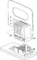
如图1所示,典型地,底板连接器系统用来将第一基片2,例如印刷电路板,平行(垂直)地连接于第二基片3,例如另一印刷电路板。随着电子元件尺寸减小和电子元件普遍变得更复杂,因此通常希望在电路板或其他基片上以更少的空间安装更多的元件。从而,希望减少底板连接器系统中的电气端子之间的间距并增加容纳在底板连接器系统中的电气端子的数量。因此,希望研发能够在速度增加的情况下运行同时还能够增加容纳在底板连接器系统中的电气端子的数量的底板连接器系统。As shown in FIG. 1, typically, a backplane connector system is used to connect a
发明内容Contents of the invention
根据本发明,一种用于安装基片的电连接器系统包括多个薄片组件。每个薄片组件包括限定了多个第一电触头通道的第一壳体、位于所述多个第一电触头通道中的第一电触头阵列、构造成与第一壳体配合的第二壳体、限定了多个第二电触头通道的第二壳体、位于多个第二电触头通道中的第二电触头阵列,以及位于多个薄片组件的安装端的组织器(organizer)。第一壳体限定了在薄片组件的安装端处从第一壳体的边缘延伸的多个凸起,并且第二壳体限定了在薄片组件的安装端处从第二壳体的边缘延伸的多个凸起。第一电触头阵列的每个电触头限定了在薄片组件的安装端处延伸过第一壳体边缘的信号基片接合元件,并且第二电触头阵列的每个电触头限定了在薄片组件的安装端处延伸过第二壳体边缘的基片接合元件。组织器限定了被做成一定尺寸以允许第一和第二电触头阵列的信号基片接合元件穿过组织器并远离组织器延伸的多个第一通孔,以及被做成一定尺寸以允许从第一和第二壳体延伸的凸起穿过组织器的多个第二通孔。According to the present invention, an electrical connector system for mounting a substrate includes a plurality of wafer assemblies. Each wafer assembly includes a first housing defining a plurality of first electrical contact channels, a first array of electrical contacts located in the plurality of first electrical contact channels, and a housing configured to cooperate with the first housing. A second housing, a second housing defining a plurality of second electrical contact channels, a second array of electrical contacts in the plurality of second electrical contact channels, and an organizer at the mounting end of the plurality of wafer assemblies (organizer). The first housing defines a plurality of protrusions extending from the edge of the first housing at the mounting end of the wafer assembly, and the second housing defines protrusions extending from the edge of the second housing at the mounting end of the wafer assembly. Multiple bumps. Each electrical contact of the first array of electrical contacts defines a signal substrate engaging element extending across the edge of the first housing at the mounting end of the wafer assembly, and each electrical contact of the second array of electrical contacts defines a A substrate engaging element extending past the edge of the second housing at the mounting end of the wafer assembly. The organizer defines a plurality of first through holes sized to allow the signal substrate engaging elements of the first and second arrays of electrical contacts to extend through the organizer and away from the organizer, and sized to The plurality of second through holes of the organizer are allowed to pass through the protrusions extending from the first and second housings.
附图说明Description of drawings
图1是将第一基片连接到第二基片的底板连接器系统的示意图;1 is a schematic diagram of a backplane connector system connecting a first substrate to a second substrate;
图2是一部分高速底板连接器系统的透视图;Figure 2 is a perspective view of a portion of the high-speed backplane connector system;
图3是图2的高速底板连接器系统的部分分解视图;Figure 3 is a partially exploded view of the high-speed backplane connector system of Figure 2;
图4是薄片组件的透视图;Figure 4 is a perspective view of a wafer assembly;
图5是图4的薄片组件的部分分解视图;Figure 5 is a partially exploded view of the wafer assembly of Figure 4;
图6A是薄片组件的中心框架的透视图;Figure 6A is a perspective view of the center frame of the wafer assembly;
图6B是薄片组件的中心框架的另一透视图;Figure 6B is another perspective view of the center frame of the wafer assembly;
图7A是图4的薄片组件的部分分解视图;Figure 7A is a partially exploded view of the wafer assembly of Figure 4;
图7B是中心框架的横截面视图;Figure 7B is a cross-sectional view of the center frame;
图8示出了封闭带形(closed band)的电配合连接器;Figure 8 shows an electrical mating connector of closed band shape (closed band);
图9A示出了三条板形(tri-beam)的电配合连接器;FIG. 9A shows an electrical mating connector of three strips (tri-beam);
图9B示出了双条板形(dual-beam)的电配合连接器;Figure 9B shows a dual-beam electrical mating connector;
图9C示出了电配合连接器另外的实施方式;Figure 9C shows an additional embodiment of an electrical mating connector;
图9D示出了电配合连接器的镜像对;Figure 9D shows a mirrored pair of electrical mating connectors;
图9E示出了电配合连接器的多个镜像对;Figure 9E shows multiple mirrored pairs of electrical mating connectors;
图10示出了多个接地片(tab);Figure 10 shows a plurality of ground tabs;
图11是接地片的透视图;Figure 11 is a perspective view of a ground lug;
图12是薄片组件的另一透视图;Figure 12 is another perspective view of the wafer assembly;
图13示出了组织器;Figure 13 shows the organizer;
图14是薄片壳体的透视图;Figure 14 is a perspective view of the wafer housing;
图15是薄片壳体的另一透视图;Figure 15 is another perspective view of the wafer housing;
图16是多个薄片组件的横截面视图;Figure 16 is a cross-sectional view of a plurality of wafer assemblies;
图17A是包括多个配合脊和多个配合凹槽的中心框架的侧视图;17A is a side view of a center frame including a plurality of mating ridges and a plurality of mating grooves;
图17B是包括多个配合脊和多个配合凹槽的多个薄片组件的横截面视图;17B is a cross-sectional view of a plurality of wafer assemblies including a plurality of mating ridges and a plurality of mating grooves;
图18A是端接头单元(header unit)的透视图;18A is a perspective view of a header unit (header unit);
图18B示出了端接头单元的配合面的一个实施方式;Figure 18B shows one embodiment of a mating surface of a termination unit;
图18C示出了端接头单元的配合面的另一个实施方式;Figure 18C shows another embodiment of the mating surface of the termination unit;
图18D示出了基本被C型接地屏蔽件和接地片围绕的一对信号管脚;Figure 18D shows a pair of signal pins substantially surrounded by a C-shaped ground shield and a ground lug;
图19A示出了端接头单元的信号管脚的一个实施方式;Figure 19A shows an embodiment of a signal pin of a termination unit;
图19B示出了端接头单元的信号管脚的另一个实施方式;Fig. 19B shows another embodiment of the signal pin of the termination unit;
图19C示出了端接头单元的信号管脚的又一个实施方式;Figure 19C shows yet another embodiment of the signal pins of the termination unit;
图19D示出了端接头单元的一对镜像的信号管脚;Figure 19D shows a pair of mirrored signal pins of a termination unit;
图20A是端接头单元的C型接地屏蔽件的透视图;Figure 20A is a perspective view of a C-type ground shield of a termination unit;
图20B是图20A的端接头单元的C型接地屏蔽件的另一视图;20B is another view of the C-type ground shield of the termination unit of FIG. 20A;
图20C示出了端接头单元的C型接地屏蔽件的另一实施方式;Figure 20C shows another embodiment of a Type C ground shield for a termination unit;
图20D示出了端接头单元的C型接地屏蔽件的又一实施方式;Figure 20D shows yet another embodiment of a Type C ground shield for a termination unit;
图20E示出了端接头单元的C型接地屏蔽件的再一实施方式;Figure 20E shows yet another embodiment of a Type C ground shield for a termination unit;
图21示出了端接头单元的接地片的一个实施方式;Figure 21 shows an embodiment of a ground lug of a termination unit;
图22是高速底板连接器系统的透视图;Figure 22 is a perspective view of the high-speed backplane connector system;
图23是图22的高速底板连接器系统的另一透视图;23 is another perspective view of the high-speed backplane connector system of FIG. 22;
图24是图22的高速底板连接器系统的又一透视图;24 is yet another perspective view of the high-speed backplane connector system of FIG. 22;
图25示出了端接头单元的安装面的一个实施方式;Figure 25 shows an embodiment of a mounting surface of a termination unit;
图26A示出了高速底板连接器系统的一个实施方式的除噪印迹(noise-cancelling footprint);Figure 26A shows the noise-cancelling footprint of one embodiment of a high-speed backplane connector system;
图26B是图26A的除噪印迹的一部分的放大视图;Figure 26B is an enlarged view of a portion of the denoised print of Figure 26A;
图27A示出了端接头单元的安装面的另一实施方式;Figure 27A shows another embodiment of the mounting surface of the termination unit;
图27B示出了图27A的端接头单元的安装面的除噪印迹;FIG. 27B shows a denoising footprint of the mounting surface of the termination unit of FIG. 27A;
图27C示出了端接头单元的安装面的又一实施方式;Figure 27C shows yet another embodiment of the mounting surface of the termination unit;
图27D示出了图27C的端接头单元的安装面的除噪阵列;Figure 27D shows the noise canceling array of the mounting surface of the termination unit of Figure 27C;
图28A示出了可与高速底板连接器系统使用的基片印迹;Figure 28A shows a substrate footprint usable with a high speed backplane connector system;
图28B示出了图28A的基片印迹的放大视图;Figure 28B shows an enlarged view of the substrate footprint of Figure 28A;
图28C示出了可与高速底板连接器系统使用的基片印迹;Figure 28C shows a substrate footprint usable with a high speed backplane connector system;
图28D示出了图28C的基片印迹的放大视图;Figure 28D shows an enlarged view of the substrate footprint of Figure 28C;
图29A示出了包括导向柱和配合键的端接头单元;Figure 29A shows an end fitting unit including a guide post and a mating key;
图29B示出了用于与图28A的端接头单元使用的薄片壳体;Figure 29B shows a wafer housing for use with the termination unit of Figure 28A;
图30A示出了多个薄片组件的安装端;Figure 30A shows the mounting end of a plurality of wafer assemblies;
图30B是图29A所示多个薄片组件的安装端的除噪印迹的一部分的放大视图;FIG. 30B is an enlarged view of a portion of the denoising footprint of the mounting end of the plurality of wafer assemblies shown in FIG. 29A;
图31A是连杆的透视图;Figure 31A is a perspective view of a linkage;
图31B示出了接合多个薄片组件的连杆;FIG. 31B shows a link engaging multiple lamellae components;
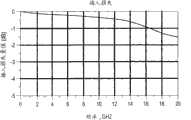
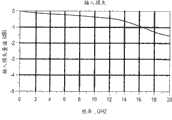
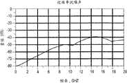
图32A是示出了图2的高速底板连接器系统的插入损耗对频率的特性图;32A is a graph showing insertion loss versus frequency characteristics of the high-speed backplane connector system of FIG. 2;
图32B是示出了图2的高速底板连接器系统的回程损耗对频率的特性图;32B is a graph showing return loss versus frequency for the high-speed backplane connector system of FIG. 2;
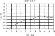
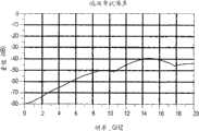
图32C是示出了图2的高速底板连接器系统的近端串扰噪声对频率的特性图;32C is a graph illustrating near-end crosstalk noise versus frequency for the high-speed backplane connector system of FIG. 2;
图32D是示出了图2的高速连接器系统的远端串扰噪声对频率的性能图;32D is a graph showing the performance of far-end crosstalk noise versus frequency for the high-speed connector system of FIG. 2;
图33是高速底板连接器系统的另一实施方式的透视图;33 is a perspective view of another embodiment of a high-speed backplane connector system;
图34是薄片组件的分解视图;Figure 34 is an exploded view of the wafer assembly;
图35A是中心框架的正透视图;Figure 35A is a front perspective view of the center frame;
图35B是中心框架的侧视图;Figure 35B is a side view of the center frame;
图35C是中心框架的后透视图;Figure 35C is a rear perspective view of the center frame;
图36示出了薄片组件的正视图和侧视图;Figure 36 shows a front view and a side view of a wafer assembly;
图37A是薄片壳体的正视图;FIG. 37A is a front view of a wafer housing;
图37B是薄片壳体的后视图;Figure 37B is a rear view of the wafer housing;
图38是多个薄片组件的横截面视图;Figure 38 is a cross-sectional view of a plurality of wafer assemblies;
图39A示出了未配合的端接头单元、薄片壳体和多个薄片组件;Figure 39A shows an unmated termination unit, wafer housing and multiple wafer assemblies;
图39B示出了配合的端接头单元、薄片壳体和多个薄片组件;Figure 39B shows a mated termination unit, wafer housing and multiple wafer assemblies;
图39C示出了未配合的端接头单元、薄片壳体和多个薄片组件的后透视图;Figure 39C shows a rear perspective view of an unmated termination unit, wafer housing and multiple wafer assemblies;
图39D示出了未配合的端接头单元、薄片壳体和多个薄片组件的放大的后透视图;Figure 39D shows an enlarged rear perspective view of an unmated termination unit, wafer housing and multiple wafer assemblies;
图40A是示出了图33的高速底板连接器系统的插入损耗对频率的特性图;40A is a graph showing insertion loss versus frequency characteristics of the high-speed backplane connector system of FIG. 33;
图40B是示出了图33的高速底板连接器系统的回程损耗对频率的特性图;40B is a graph illustrating return loss versus frequency characteristics of the high-speed backplane connector system of FIG. 33;
图40C是示出了图33的高速底板连接器系统的近端串扰噪声对频率的特性图;40C is a graph showing near-end crosstalk noise versus frequency for the high-speed backplane connector system of FIG. 33;
图40D是示出了图33的高速连接器系统的远端串扰噪声对频率的特性图;40D is a graph showing far-end crosstalk noise versus frequency for the high-speed connector system of FIG. 33;
图41是高速底板连接器的另一实施方式的透视图以及部分分解视图;Figure 41 is a perspective view and a partially exploded view of another embodiment of a high-speed backplane connector;
图42是图41的高速底板连接器的另一透视图以及部分分解视图;Figure 42 is another perspective view and a partially exploded view of the high-speed backplane connector of Figure 41;
图43A是薄片组件的透视图;Figure 43A is a perspective view of a wafer assembly;
图43B是薄片组件的部分分解视图;Figure 43B is a partially exploded view of the wafer assembly;
图44A是壳体和嵌入的接地框架的透视图;Figure 44A is a perspective view of the housing and embedded ground frame;
图44B是可位于壳体一侧的接地框架的透视图;Figure 44B is a perspective view of a ground frame that may be located on one side of the housing;
图44C是具有位于壳体一侧的接地框架的薄片组件的透视图;Figure 44C is a perspective view of a wafer assembly with a ground frame on one side of the housing;
图45是薄片组件的横截面视图;Figure 45 is a cross-sectional view of a wafer assembly;
图46示出了薄片组件的正视图和侧视图;Figure 46 shows a front view and a side view of a wafer assembly;
图47A示出了接地屏蔽件的一个实施方式;Figure 47A shows an embodiment of a ground shield;
图47B示出了组装后的薄片组件,该薄片组件具有跨接了两个电配合连接器且为第一和第二壳体电气共用的接地屏蔽件;Figure 47B shows the assembled wafer assembly with a ground shield spanning the two electrically mating connectors and electrically common to the first and second housings;
图47C和47D是组装后的薄片组件的另一些图示,该薄片组件具有跨接了两个电配合连接器且为第一和第二壳体电气共用的接地屏蔽件;47C and 47D are further illustrations of an assembled wafer assembly having a ground shield spanning two electrically mating connectors and electrically common to the first and second housings;
图48A是端接头单元的配合面的透视图;Figure 48A is a perspective view of a mating face of a termination unit;
图48B是薄片壳体的配合面的透视图;Figure 48B is a perspective view of the mating face of the wafer housing;
图49示出了两个相邻薄片组件之间的气隙;Figure 49 shows an air gap between two adjacent lamella assemblies;
图50A是未配合的高速底板连接器系统的透视图;Figure 50A is a perspective view of an unmated high-speed backplane connector system;
图50B是配合后的高速底板连接器系统的透视图;Figure 50B is a perspective view of the mated high-speed backplane connector system;
图51A是多个薄片组件与组织器的透视图;Figure 51A is a perspective view of a plurality of wafer assemblies and organizer;
图51B是多个薄片组件与组织器的另一透视图;51B is another perspective view of a plurality of wafer assemblies and organizer;
图52A是安装面组织器的一个实施方式的透视图;Figure 52A is a perspective view of one embodiment of a mounting surface organizer;
图52B是图52A的安装面组织器的放大视图,该安装面组织器位于多个薄片组件的安装面处;52B is an enlarged view of the mounting surface organizer of FIG. 52A positioned at the mounting surface of a plurality of wafer components;
图52C是图41的高速底板连接器的透视图,该高速底板连接器具有图52A的安装面组织器;52C is a perspective view of the high-speed backplane connector of FIG. 41 having the mounting surface organizer of FIG. 52A;
图53A是安装面组织器的另一实施方式的透视图;Figure 53A is a perspective view of another embodiment of a mounting surface organizer;
图53B示出了在多个薄片组件的安装端处由延伸过图53A的安装面组织器的多个凸起所产生的气隙;Figure 53B illustrates the air gap created by the plurality of protrusions extending through the mounting surface organizer of Figure 53A at the mounting end of the plurality of wafer components;
图53C和53D是延伸过图53A的安装面组织器的多个凸起的另外的图示;53C and 53D are additional illustrations of a plurality of protrusions extending across the mounting surface organizer of FIG. 53A;
图54A是示出了图41的高速底板连接器系统的插入损耗对频率的特性图;54A is a graph showing insertion loss versus frequency characteristics of the high-speed backplane connector system of FIG. 41;
图54B是示出了图41的高速底板连接器系统的回程损耗对频率的特性图;54B is a graph illustrating return loss versus frequency characteristics of the high-speed backplane connector system of FIG. 41;
图54C是示出了图41的高速底板连接器系统的近端串扰噪声对频率的特性图;54C is a graph showing near-end crosstalk noise versus frequency for the high-speed backplane connector system of FIG. 41;
图54D是示出了图41的高速连接器系统的远端串扰噪声对频率的特性图;FIG. 54D is a graph showing far-end crosstalk noise versus frequency for the high-speed connector system of FIG. 41;
图55是高速底板连接器系统的另一实施方式的一部分的透视图;Figure 55 is a perspective view of a portion of another embodiment of a high-speed backplane connector system;
图56A是接地屏蔽件的透视图;Figure 56A is a perspective view of a ground shield;
图56B是多个壳体组件的透视图;Figure 56B is a perspective view of a plurality of housing assemblies;
图56C是接地屏蔽件的另一透视图;Figure 56C is another perspective view of a ground shield;
图57A示出了多个未弯曲的电触头组件;Figure 57A shows a plurality of unbent electrical contact assemblies;
图57B示出了多个弯曲的电触头组件;Figure 57B illustrates a plurality of curved electrical contact assemblies;
图58是电配合连接器的差分对的放大视图;Figure 58 is an enlarged view of a differential pair of an electrically mating connector;
图59示出了接地屏蔽件的安装端的除噪印迹以及电触头组件的矩阵;Figure 59 shows a noise canceling footprint of a mounting end of a ground shield and a matrix of electrical contact assemblies;
图60是安装端组织器的正视图;Figure 60 is a front view of the mounting end organizer;
图61A是高速底板连接器系统的一部分的侧视图;Figure 61A is a side view of a portion of a high-speed backplane connector system;
图61B是高速底板连接器系统的一部分的透视图;Figure 61B is a perspective view of a portion of the high-speed backplane connector system;
图62示出了接地屏蔽件和与端接头单元配合的多个薄片组件;Figure 62 shows a ground shield and a plurality of wafer assemblies mated with a termination unit;
图63A是示出了图55的高速底板连接器系统的插入损耗对频率的特性图;63A is a graph showing insertion loss versus frequency characteristics of the high-speed backplane connector system of FIG. 55;
图63B是示出了图55的高速底板连接器系统的回程损耗对频率的特性图;63B is a graph illustrating return loss versus frequency characteristics of the high-speed backplane connector system of FIG. 55;
图63C是示出了图55的高速底板连接器系统的近端串扰噪声对频率的特性图;63C is a graph showing near-end crosstalk noise versus frequency for the high-speed backplane connector system of FIG. 55;
图63D是示出了图55的高速连接器系统的远端串扰噪声对频率的特性图;FIG. 63D is a graph showing far-end crosstalk noise versus frequency for the high-speed connector system of FIG. 55;
图64是多个薄片组件的配合端的图示;Figure 64 is an illustration of the mating ends of a plurality of wafer components;
图65是多个薄片组件的配合端的另一图示;Figure 65 is another illustration of the mating end of a plurality of wafer components;
图66A是头部组件的透视图;Figure 66A is a perspective view of a head assembly;
图66B是图66A的头部组件的侧视图;Figure 66B is a side view of the head assembly of Figure 66A;
图67示出了图66A和66B的头部组件的安装管脚布局;Figure 67 shows the mounting pin layout of the header assembly of Figures 66A and 66B;
图68是多个薄片组件的一个实施方式的配合端的图示;Figure 68 is an illustration of the mating end of one embodiment of a plurality of wafer assemblies;
图69是多个薄片组件的另一实施方式的配合端的图示;Figure 69 is an illustration of the mating end of another embodiment of a plurality of wafer assemblies;
图70是多个薄片组件的又一实施方式的配合端的图示;Figure 70 is an illustration of the mating end of yet another embodiment of a plurality of wafer components;
图71A是示出了包括图66-70的薄片组件设计的高速底板连接器系统的插入损耗对频率的特性图;71A is a graph showing insertion loss versus frequency characteristics for a high-speed backplane connector system including the wafer assembly design of FIGS. 66-70;
图71B是示出了包括图66-70的薄片组件设计的高速底板连接器系统的回程损耗对频率的特性图;71B is a graph illustrating return loss versus frequency for a high-speed backplane connector system including the wafer assembly design of FIGS. 66-70;
图71C是示出了包括图66-70的薄片组件设计的高速底板连接器系统的近端串扰噪声对频率的特性图;71C is a graph showing near-end crosstalk noise versus frequency for a high-speed backplane connector system including the wafer assembly design of FIGS. 66-70;
图71D是示出了包括图66-70的薄片组件设计的高速连接器系统的远端串扰噪声对频率的特性图。71D is a graph showing far-end crosstalk noise versus frequency for a high-speed connector system including the wafer assembly design of FIGS. 66-70.
具体实施方式Detailed ways
该公开内容致力于用于安装基片的高速底板连接器系统,该高速底板连接器系统能够在高达至少25Gbps的速度下操作,同时,在一些实施方式中,还提供了每英寸至少50对电连接器的管脚密度。如下面更详细的解释,公开的高速连接器系统的实施方式可以提供接地屏蔽件和/或其他接地结构,其穿过底板印迹、底板连接器和子卡印迹以三维方式大致封装可为差分的电连接器对的电连接器对。这些封装的接地屏蔽件和/或接地结构,连同包围电连接器对本身的不同凹槽的绝缘填料一起,防止当高速底板连接器系统以高达至少30GHz的频率操作时不希望有非横向的、纵向的且高次的模式传播。This disclosure is directed to a high-speed backplane connector system for mounting substrates capable of operating at speeds up to at least 25 Gbps while, in some embodiments, also providing at least 50 electrical pairs per inch. Connector pin density. As explained in more detail below, embodiments of the disclosed high-speed connector system may provide ground shields and/or other ground structures that generally encapsulate electrical circuits that may be differential in three dimensions through the backplane footprint, backplane connector, and daughtercard footprint. Electrical connector pair for connector pair. The ground shields and/or ground structures of these packages, together with the insulating filler surrounding the various grooves of the electrical connector pair itself, prevent undesirable non-lateral, Longitudinal and higher order mode propagation.
而且,如下面更详细的解释,公开的高速连接器系统的实施方式可以在电连接器对的每个连接器之间提供大致相同的几何结构以防止纵向模变。Furthermore, as explained in more detail below, embodiments of the disclosed high-speed connector system can provide approximately the same geometry between each connector of an electrical connector pair to prevent longitudinal mold.
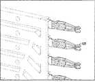
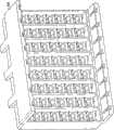
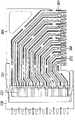
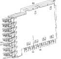
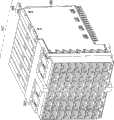
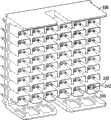
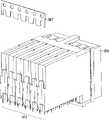
根据图2-32描述了第一高速底板连接器系统100。高速底板连接器100包括多个薄片组件102,如下面更详细的解释,通过薄片壳体104而使该多个薄片组件102彼此相邻地定位在连接器系统100中。The first high speed
多个薄片组件102中的每个薄片组件106包括中心框架108、第一电触头阵列110(也称为第一引线框架组件)、第二电触头阵列112(也称为第二引线框架组件)、多个接地片132以及组织器134。在一些实施方式中,中心框架108包括电镀塑料或压铸的接地薄片,例如在镍(Ni)上镀锡(Sn)或者锌(Zn)压铸件,并且第一和第二电触头阵列110、112包括磷青铜和在镍(Ni)镀层上的金(Au)或锡(Sn)镀层。但是,在其他实施方式中,中心框架108可包括铝(Al)压铸件、导电的聚合物、金属注射成型或者其他类型的金属;第一和第二电触头阵列110、112可包括任意的铜(Cu)合金材料;并且镀层金属可以是任何贵金属,例如Pd,或者是合金,诸如Pd-Ni、或者在接触区域中薄镀Au的Pd、在安装区域中薄镀Au的锡(Sn)或镍(Ni)、以及在底板或底座中薄镀Au的镍(Ni)。Each
中心框架108限定了第一侧114和与第一侧114相对的第二侧116。第一侧114包括限定了多个第一通道118的导电表面。在一些实施方式中,多个第一通道118中的每个通道覆盖有绝缘层119,例如过模制的塑料绝缘体,从而当第一电触头阵列110基本位于多个第一通道118中时,绝缘层119将电触头与第一侧114的导电表面电隔离。The
类似地,第二侧116也包括限定了多个第二通道120的导电表面。如同一些实施方式中的多个第一通道118一样,多个第二通道120中的每个通道覆盖有绝缘层121,例如过模制的塑料绝缘体,从而当第二电触头阵列112基本位于多个第二通道120中时,绝缘层121将电触头与第二侧116的导电表面电隔离。Similarly,
如图7B所示,在一些实施方式中,中心框架包括位于第一和第二侧114、116之间的嵌入的导电屏蔽115。将导电屏蔽115电连接到第一侧114的导电表面和第二侧116的导电表面。As shown in FIG. 7B , in some embodiments, the center frame includes an embedded
参照图4,当组装时,将第一电触头阵列110大致定位在中心框架108的第一侧114的多个通道118中,并且将第二电触头阵列112大致定位在中心框架108的第二侧116的多个通道120中。当定位在多个通道118、120中时,第一电触头阵列110中的每个电触头被定位成邻近第二电触头阵列112的电触头。在一些实施方式中,将第一和第二电触头阵列110、112定位在多个通道118、120中,从而相邻的电触头之间的距离在整个薄片组件106内基本相同。第一和第二电触头阵列110、112的相邻电触头形成电触头对130。在一些实施方式中,电触头对130可以是差分的电触头对。Referring to FIG. 4 , when assembled, the first array of
当定位在多个通道118、120中时,第一和第二电触头阵列110、112的电配合连接器129远离薄片组件106的配合端131延伸。在一些实施方式中,电配合连接器129是如图7A和8所示的封闭带形;在其他实施方式中,电配合连接器129是如图9A所示的三条板形,或者如图9B所示的双条板形。其他的配合连接器形式可以具有多个条板。图9C示出了电配合连接器129的其他实施方式的例子。When positioned in the plurality of
将认识到,三条板形、双条板形或封闭带形的电配合连接器129在多尘环境中提供了改进的可靠性;在不稳定的环境中提供了改进的性能,例如摆动或物理震动的环境中,提供了改进的性能;由于并联的电气路径而导致较低的接触电阻;并且由于能量趋于从具有较像盒子的几何形状的电配合连接器129的尖角辐射,所以封闭带形或三条板形的设置提供了改进的电磁性质。It will be appreciated that
参照图9D和9E,在一些实施方式中,对于每个电触头对130,第一电触头阵列110的电触头与相邻的第二电触头阵列112的电触头呈镜像。将认识到,使电触头对的电触头呈镜像在制造以及用于高速电气性能的列对列一致性方面提供了好处,同时,还在成对的两列中提供了唯一结构。Referring to FIGS. 9D and 9E , in some embodiments, for each
当定位在多个通道118、120中时,第一和第二电触头阵列110、112的基片接合元件172,例如电触头安装管脚,也远离薄片组件106的安装端170延伸。When positioned in the plurality of
第一电触头阵列110包括第一隔板122和第二隔板124以适当隔开每个电触头,用于大致插入到多个第一通道118中。类似地,第二电触头阵列112包括第一隔板126和第二隔板128以适当隔开每个电触头,用于插入到多个第二通道120中。在一些实施方式中,第一电触头阵列110的第一和第二隔板122、124以及第二电触头阵列112的第一和第二隔板126、128包括模制的塑料。第一和第二电触头阵列110、112基本位于多个通道118、120中,第一电触头阵列110的第一隔板122邻接第二电触头阵列112的第一隔板126。The first array of
在一些实施方式中,第一电触头阵列110的第一隔板122可以限定齿形的侧面或者波浪形的侧面,并且第二电触头阵列的第一隔板126可以限定互补的齿形侧面或者互补的波浪形侧面,从而当第一隔板122、126邻接时,第一隔板122、126的互补侧面接合并配合。In some embodiments, the first partition 122 of the first array of
如图4、10和11所示,将多个接地片132定位在薄片组件106的配合端131处以远离中心框架108延伸。将接地片132电连接到中心框架108的第一和第二侧114、116中的至少一侧。典型地,接地片132是桨形,并且至少一个接地片132在薄片组件的配合端131处位于每个电触头对130的上面和下面。在一些实施方式中,接地片包括在镍(Ni)镀层上镀锡(Sn)的黄铜或者其他导电的镀层或贱金属。As shown in FIGS. 4 , 10 and 11 , a plurality of
组织器134位于薄片组件106的配合端131处。组织器包括多个通孔135,当组织器134位于薄片组件106的配合端131时,该多个通孔135允许从薄片组件106延伸的电配合连接器129和接地片132穿过组织器134。组织器用于将中心框架108、第一电触头阵列110、第二电触头阵列112和接地片132牢固地锁定在一起。An
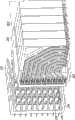
参照附图2和3,薄片壳体104在每个薄片组件106的配合端131处接合多个薄片组件102。薄片壳体104接收从多个薄片组件102延伸的电配合连接器129和接地片132,并且使每个薄片组件106与多个薄片组件102中的另一个薄片组件106相邻定位。如图16所示,当彼此相邻定位时,两个薄片组件106限定了基本在第一薄片组件106的一段电触头与第二薄片组件106的一段电触头之间的多个气隙134。每个气隙134用来使采用薄片组件106的气隙134进行定位的电触头电隔离。Referring to FIGS. 2 and 3 , the
参照图17A和17B,在一些实施方式中,每个中心框架108限定了从中心框架108的第一侧114延伸的多个配合脊109以及从中心框架108的第二侧116延伸的多个配合脊109。此外,每个中心框架在中心框架108的第一侧114处限定了多个配合凹槽111并在中心框架108的第二侧116处限定了多个配合凹槽111。17A and 17B, in some embodiments, each
如图17A所示,在一些实施方式中,将一个配合脊109和一个配合凹槽111定位在中心框架108的第二侧116上的多个第二通道120中的每个通道之间。而且,将与第二侧的配合脊109和配合凹槽111互补的配合脊109和配合凹槽111定位在中心框架108的第一侧114上的多个第一通道118中的每个通道之间。因此,如图17B所示,当两个薄片组件106在薄片壳体104中彼此相邻定位时,从第一薄片组件106的第一侧114延伸的配合脊109接合位于第二相邻薄片组件106的第二侧116上的配合凹槽111,并且从第二薄片组件106的第二侧116延伸的配合脊109接合位于相邻的第一薄片组件106的第一侧114上的配合凹槽111。As shown in FIG. 17A , in some embodiments, a
最终的重叠部分113在相邻的薄片组件106之间提供了改进的接触。此外,最终的重叠部分113中断了相邻的气隙134之间的直接信号路径,从而改进了在位于气隙134中的第一和第二电触头阵列110、112的电触头上传播的信号的性能。The resulting overlapping
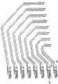
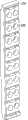
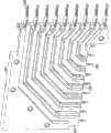
如图18-23所示,连接器系统100还包括适于与薄片壳体104配合的端接头模块136。与薄片壳体104接合的端接头模块136的配合面包括多个C型接地屏蔽件138、一排接地片140以及多个信号管脚对142。在一些实施方式中,端接头模块136可包括液晶聚合物(LCP)绝缘体;信号管脚对142包括磷青铜基材料,以及在镍(Ni)镀层上的金(Au)和锡(Sn)镀层;并且接地屏蔽件138和接地片140包括锡(Sn)镀层在镍(Ni)镀层之上的黄铜基材料。可以使用其他导电的基体材料和镀层(贵金属或非贵金属)构造信号管脚、接地屏蔽件和接地片。可以使用其他聚合物构造壳体。As shown in FIGS. 18-23 , the
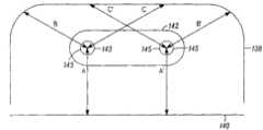
如图18A和18B所示,沿端接头模块136的配合面的一侧定位接地片排140。在C型接地屏蔽件138的开口端处将多个C型接地屏蔽件138中的第一排144定位在那排接地片140之上,以使多个信号管脚对142中的信号管脚对146基本被接地片和C型接地屏蔽件包围。
在第二排148的C型接地屏蔽件的开口端处将多个C型接地屏蔽件138中的第二排148定位在多个C型接地屏蔽件138中的第一排144之上,以使多个信号管脚对142中的信号管脚对150基本被第一排144的C型接地屏蔽件和第二排148的C型接地屏蔽件的边缘包围。将认识到,重复该模式,以使每个随后的信号管脚对142基本被第一C型接地屏蔽件和第二C型接地屏蔽件的边缘包围。Positioning the second row 148 of the plurality of Type-C ground shields 138 above the first row 144 of the plurality of Type-C ground shields 138 at the open ends of the Type-C ground shields of the second row 148 to The signal pin pair 150 of the plurality of signal pin pairs 142 is substantially surrounded by the edges of the Type-C ground shields of the first row 144 and the Type-C ground shields of the second row 148 . It will be appreciated that this pattern is repeated such that each subsequent pair of signal pins 142 is substantially surrounded by the edges of the first Type-C ground shield and the second Type-C ground shield.
将那排接地片140和多个C型接地屏蔽件138定位在端接头模块136上,从而当端接头模块136与多个薄片组件102以及薄片壳体配合时,如下面更详细的描述,每个C型接地屏蔽件是水平的并垂直于薄片组件106,并且横跨薄片组件106的第一电触头阵列110的电触头和第二电触头阵列的电触头。The row of ground lugs 140 and the plurality of C-shaped ground shields 138 are positioned on the
如图18D所示,将每个信号管脚对142定位在端接头模块136上,以使信号管脚对的第一信号管脚143与C型接地屏蔽件或接地片上的一点之间的距离(参见距离a、b和c)基本等于信号管脚对的第二信号管脚145与C型接地屏蔽件或接地片上的对应点之间的距离(参见a’、b’和c’)。在第一和第二信号管脚143、145与C型接地屏蔽件或接地片之间的对称性改进了在信号管脚对142上传播信号的操纵灵活性。As shown in FIG. 18D , each
在一些实施方式中,多个信号管脚对142中的每个信号管脚是直立的圆形管脚,如图19A所示,从而当端接头模块136接收薄片壳体104时,薄片壳体104接收多个信号管脚对142,并且从多个薄片组件102延伸的第一和第二电触头阵列110、112的电配合连接器129接收并接合多个信号管脚对142。然而,在其他实施方式中,多个信号管脚对142的每个信号管脚是直立的U型管脚,如图19B或19C所示。将认识到,因为不需要双规格材料来制造配合端和安装端,所以U型管脚提供了高效的制造。In some embodiments, each signal pin in the plurality of signal pin pairs 142 is an upright circular pin, as shown in FIG. 104 receives a plurality of signal pin pairs 142 and the
参照图19D,在一些实施方式中,对于每个信号管脚对142,信号管脚对的第一信号管脚143与信号管脚对的相邻第二信号管脚145呈镜像。将认识到,信号管脚对142的信号管脚呈镜像在制造以及高速电气性能方面提供了好处,同时还提供了信号管脚对的唯一结构。Referring to FIG. 19D , in some embodiments, for each
在一些实施方式中,端接头模块136中的每个C型接地屏蔽件138和每个接地片140可包括一个或多个配合接口152,如图20A、20B、20C、20D、20E和21所示。因此,如图22-24所示,当端接头模块136接收薄片壳体104时,薄片壳体104接收端接头模块136的接地屏蔽件138和接地片140,并且端接头模块136的C型接地屏蔽件138和接地片140在至少一个或多个配合接口152处接合从多个薄片组件102延伸的接地片132。In some embodiments, each C-shaped
将认识到,当端接头模块136与薄片壳体104以及多个薄片组件102配合时,接合的信号管脚对142与第一和第二电触头阵列110、112的电配合连接器129中的每组基本被薄片组件106的接地片132、端接头模块136的C型接地屏蔽件136以及端接头模块136的接地片140或端接头模块136的另一个C型接地屏蔽件136的一侧之一包围并电隔离。It will be appreciated that when the
如图19-21所示,端接头模块136的每个C型接地屏蔽件和接地片还限定了一个或多个基片接合元件156,例如接地安装管脚,将每个基片接合元件构造成在基片的通孔处接合基片。而且,端接头模块136的每个信号管脚还限定了基片接合元件158,例如信号安装管脚,将该基片接合元件构造成在基片的通孔处接合基片。在一些实施方式中,每个接地安装管脚156和信号安装管脚158限定了宽边161以及比宽边161小的边缘163。As shown in FIGS. 19-21 , each C-type ground shield and ground lug of the
接地安装管脚156和信号安装管脚158延伸过端接头模块136,并且远离端接头模块136的安装面延伸。接地安装管脚156和信号安装管脚158用于接合基片,例如底板电路板或子卡电路板。The
在一些实施方式中,每对信号安装管脚158被定位在两个取向中的一个取向上,例如耦合的宽边或耦合的边缘。在其他的实施方式中,每对信号安装管脚156被定位在两个取向中的一个取向上,其中在第一取向,对齐一对信号安装管脚158从而使该对的宽边161基本平行于基片,而在第二取向,对齐一对信号安装管脚158从而使该对的宽边161基本垂直于基片。如上关于图9D和9E所述,可以将一对信号安装管脚158的信号管脚定位在端接头模块136上,以使信号安装管脚对158的一个信号管脚与那对信号安装管脚158的相邻信号管脚呈镜像。In some implementations, each pair of
在一些实施方式中,如图25、26A和26B所示,可以将接地安装管脚156和信号安装管脚158定位在端接头模块136上以生成除噪印迹159。参照图26B,在除噪印迹159中,一对信号安装管脚160的取向从每对相邻的信号安装管脚162的取向偏移,该相邻的信号安装管脚对没有通过接地安装管脚163与信号安装管脚160分开。例如,一对信号安装管脚160的取向可以从没有通过接地安装管脚163与信号安装管脚对160分开的每对信号安装管脚162的取向偏移90度。In some embodiments, as shown in FIGS. 25 , 26A and 26B ,
在印迹的其他实施方式中,如图27A和27B所示,在相同的取向上定位每对信号安装管脚158。然后,将具有多个接地安装管脚156的C型接地屏蔽件138和接地片140定位在如上所述的信号管脚对142的周围。定位C型接地屏蔽件138和接地片140的接地安装管脚156使得至少一个接地安装管脚156位于第一信号管脚对142的信号安装管脚158与相邻信号管脚对142的信号安装管脚158之间。在一些实施方式中,除了如图27A和27B所示的接地安装管脚外,C型接地屏蔽件138和接地片140可包括定位在位置157处的接地安装管脚156。In other embodiments of the footprint, as shown in Figures 27A and 27B, each pair of
在印迹的另外实施方式中,如图27C和27D所示,在相同的取向上定位每对信号安装管脚158。然后,将具有多个接地安装管脚156的C型接地屏蔽件138和接地片140定位在如上所述的信号管脚对142的周围。定位接地安装管脚156使得至少一个接地安装管脚156位于第一信号管脚对142的信号安装管脚158与相邻信号管脚对142的信号安装管脚158之间。In an alternative embodiment of the footprint, each pair of
将认识到,将接地安装管脚156定位在信号安装管脚158之间减少了信号安装管脚158之间的串扰量。当沿信号管脚对142的信号管脚传播的信号干扰了沿另一信号管脚对142的信号管脚传播的信号时,串扰就发生了。It will be appreciated that positioning the
典型地,根据如上所述的印迹,端接头模块136的信号安装管脚158在定位于基片上的多个第一通孔处接合基片,其中将多个第一通孔设置成行和列的矩阵,并且能够提供电连接器的安装。每个第一通孔与其最紧密相邻的第一通孔中的一个结合,以形成第一通孔对。将第一通孔对构造成接收一个信号管脚对142的信号安装管脚158。端接头模块136的C型接地屏蔽件138和接地片140的接地安装管脚156在定位于基片上的多个第二通孔处接合基片。将多个第二通孔构造成彼此电气共用以提供公共接地,并且定位在多个第一通孔之间以使至少一个第二通孔直接定位在每个第一通孔和最紧密相邻的非成对第一通孔中的任一个之间。Typically, the
图28A、28B、28C和28D示出了,可以接收端接头模块156的安装端或者如下面更详细解释的多个薄片组件102的安装端的基片印迹的例子。将认识到,基片印迹应该能够保持系统的阻抗,例如100欧姆不等,同时还使对到对的串扰噪声最小。基片印迹还应该为差分对提供足够的线路通道,同时保留不歪斜的线路和连接器设计。对于高密度的基片印迹来说,应该完成这些任务,同时注意基片纵横比的限制,为了确保可靠的制造,通孔必须足够大(给定的基片厚度)。Figures 28A, 28B, 28C and 28D illustrate examples of substrate footprints that may receive the mounting end of an
图28A和28B示出了可实现所述任务的最优化的按行差分(in-row-differential)的基片印迹的一个实施方式。该基片印迹被“按行”取向以便减少或消除线路歪斜和连接器歪斜。而且,基片印迹通过将用于连接器接地屏蔽件的触头165的多点设置到在用于信号管脚或电触头的触头167的点周围的印刷电路板来改进性能。此外,基片印迹提供了将来自8行印迹的所有差分对仅布线于四个层中同时使层内、层间以及迹线到筒体(trace-to-barrel)的布线噪声最小的能力。Figures 28A and 28B illustrate one embodiment of an optimized in-row-differential substrate footprint that can accomplish the described task. The substrate footprint is oriented "in-row" to reduce or eliminate line skew and connector skew. Also, the substrate footprint improves performance by providing multiple points for
基片印迹使对到对的串扰最小在于来自20ps(20-80%)边缘的全部同步的、多入侵的、最坏情形的串扰大约为1.90%(远端噪声)。而且,印迹被布置成以使多数的远端噪声来自“行内”的入侵,这意味着诸如列阵的发送器/接收器的管脚引线和特定层的线路的设计会将印迹的噪声减少至小于0.50%。在一些实施方式中,在每英寸52.1对通孔下,基片印迹提供了具有超过80欧姆阻抗的8行印迹,从而在100欧姆的额定系统环境中保持了不同的插入损耗值。在该实施方式中,可以使用18密耳(mil)直径的钻孔机来生成基片印迹的通孔,对于0.250英寸厚的基片,保持纵横比小于14∶1。The substrate footprint minimizes pair-to-pair crosstalk in that the all simultaneous, multi-aggressive, worst case crosstalk from a 20 ps (20-80%) edge is about 1.90% (far-end noise). Also, the footprint is arranged so that most of the far-end noise comes from "in-row" intrusions, which means that design such as the array's transmitter/receiver pinouts and layer-specific wiring reduces the footprint's noise to Less than 0.50%. In some embodiments, at 52.1 via pairs per inch, the substrate footprint provides 8 rows of footprints with an impedance in excess of 80 ohms, maintaining different insertion loss values in a nominal system environment of 100 ohms. In this embodiment, an 18 mil diameter drill can be used to create via holes for the substrate footprint, maintaining an aspect ratio of less than 14:1 for a 0.250 inch thick substrate.
图28C和28D示出了最优化的按行差分的基片印迹的另一个实施方式。与图28A和28B的基片印迹相比,基片印迹中的相邻列彼此偏移以便使噪声最小化。类似于上述的基片印迹,该基片印迹“按行”取向以便减少或消除线路歪斜和连接器歪斜;通过将用于连接器接地屏蔽件的触头165的多点设置到在用于信号管脚或电触头的触头167的点周围的印刷电路板,该基片印迹提供了改进的性能;而且,提供了只在4层中将所有的差分对布线出8行印迹同时使内部层、里层以及迹线到筒体的布线噪声最小的能力。Figures 28C and 28D illustrate another embodiment of an optimized row-by-row differential substrate footprint. Adjacent columns in the substrate footprint are offset from each other in order to minimize noise compared to the substrate footprint of Figures 28A and 28B. Similar to the substrate footprint described above, the substrate footprint is oriented "in rows" to reduce or eliminate line skew and connector skew; The printed circuit board around the point of the
基片印迹使对到对的串扰最小在于来自20ps(20-80%)边缘的全部同步的、多入侵的、最坏情形的串扰大约为0.34%(远端噪声)。在一些实施方式中,在每英寸52.1对通孔下,基片印迹提供了大约95欧姆的阻抗。在一些实施方式中,可以用13密耳直径的钻孔机来生成基片印迹的通孔,对于0.150英寸厚的基片,保持纵横比小于12∶1。The substrate footprint minimizes pair-to-pair crosstalk in that the all-synchronous, multi-aggressive, worst-case crosstalk from a 20 ps (20-80%) edge is about 0.34% (far-end noise). In some embodiments, the substrate footprint provides an impedance of approximately 95 ohms at 52.1 via pairs per inch. In some embodiments, a 13 mil diameter drill can be used to create via holes for the substrate footprint, maintaining an aspect ratio of less than 12:1 for a 0.150 inch thick substrate.
将认识到,虽然根据本申请中描述的高速连接器系统已描述了图27A、27B、27C和27D的印迹,但是,这些相同的印迹可以与连接到诸如印刷电路板的基片的其他模块一起使用。It will be appreciated that although the footprints of Figures 27A, 27B, 27C, and 27D have been described in accordance with the high-speed connector system described in this application, these same footprints may be used with other modules connected to a substrate such as a printed circuit board. use.
参照图29A和29B,在一些实施方式中,为了改进薄片壳体104和端接头模块136之间的配合对齐,端接头模块136可包括导向柱164,并且薄片壳体104可包括导向凹槽166,当薄片壳体104与端接头模块136配合时,导向凹槽166接收导向柱164。通常,导向柱164和相应的导向凹槽166接合以在薄片壳体104与端接头模块136配合之前提供初始定位。Referring to FIGS. 29A and 29B , in some embodiments, to improve mating alignment between the
而且,在一些实施方式中,端接头模块136还可包括配合键168,并且薄片壳体104可包括互补的键孔凹槽170,当薄片壳体104与端接头模块136配合时,键孔凹槽170接收配合键168。典型地,可以旋转配合键168和互补的键孔凹槽170以在不同位置设置互补的键。薄片壳体104和端接头模块136可包括配合键168和互补的键孔凹槽170以控制哪个薄片壳体104与哪个端接头模块136配合。Furthermore, in some embodiments, the
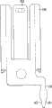
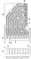
参照如图30A所示的多个薄片组件102的安装端170,第一和第二电触头阵列110、112的电触头安装管脚172从薄片组件102延伸。此外,多个连杆174定位在多个薄片组件102的安装端170处。Referring to the mounting end 170 of the plurality of
图31A详细所示的每个连杆176包括多个基片接合元件178,例如接地安装管脚,以及多对接合片180。将每个连杆174定位成穿过多个薄片组件102,从而使连杆174接合每个薄片组件。具体地,如图31B所示,每对接合片180用一对接合片174的第一片182和该对接合片174的第二片184接合不同的薄片组件106,第一片182位于中心框架108的一侧,第二片184位于中心框架108的另一侧。Each
电触头安装管脚172从多个薄片组件102延伸,并且接地安装管脚178从多个连杆174延伸,以接合基片,例如现有技术已知的底板电路板或子卡电路板。如上所述,每个电触头安装管脚172和每个接地安装管脚可以限定宽边161和比宽边161小的边缘163。Electrical
在一些实施方式中,对应于电触头对130的每对电触头安装管脚172被定位在两个取向中的一个取向上,例如耦合的宽边或耦合的边缘。在其他的实施方式中,对应于电触头对130的每对电触头安装管脚172被定位在两个取向中的一个取向上,其中,在第一取向,对齐一对电触头安装管脚172从而使管脚的宽边161基本与基片平行,而在第二取向,对齐一对电触头安装管脚172从而使宽边161基本垂直于基片。In some embodiments, each pair of electrical
还可将电触头安装管脚172和接地安装管脚178另外定位在多个薄片组件102的安装端170处,如图29所示,以生成除噪印迹。类似于上面所述的关于端接头模块136的除噪印迹,在多个薄片组件102的安装端170处的除噪印迹中,一对电触头安装管脚182的取向从每个相邻的电触头安装管脚对184的取向偏移,每个相邻的电触头安装管脚对184没有通过接地安装管脚186与电触头安装管脚对182分开。Electrical
图32A、32B、32C和32D是示出了上面关于图2-31所述的电连接器系统的近似特性的曲线图。图32A是示出了电连接器系统的插入损耗对频率的特性图;图32B是示出了电连接器系统的回程损耗对频率的特性图;图32C是示出了电连接器系统的近端串扰噪声对频率的特性图;图32D是示出了电连接器系统的远端串扰噪声对频率的特性图。如图32A、32B、32C和32D所示,电连接器系统给在以高达至少25Gbps的速度操作的第一和第二电触头阵列110、112的电触头上负载的电信号提供了大致相同的阻抗分布图。32A, 32B, 32C and 32D are graphs showing approximate characteristics of the electrical connector system described above with respect to FIGS. 2-31. 32A is a characteristic diagram showing the insertion loss of the electrical connector system versus frequency; FIG. 32B is a characteristic diagram showing the return loss of the electrical connector system versus frequency; FIG. Figure 32D is a characteristic diagram showing the far-end crosstalk noise of the electrical connector system versus frequency. As shown in Figures 32A, 32B, 32C and 32D, the electrical connector system provides approximately The same impedance profile.
根据图33-40描述了高速底板连接器系统200的其他实施方式。类似于上面关于图2-32所述的连接器系统100,高速底板连接器200包括通过薄片壳体204在连接器系统200中彼此相邻定位的多个薄片组件202。Other embodiments of the high-speed backplane connector system 200 are described with respect to FIGS. 33-40 . Similar to the
多个薄片组件202中的每个薄片组件206包括中心框架208、第一电触头阵列210、第二电触头阵列212、第一接地屏蔽件引线框架214以及第二接地屏蔽件引线框架216。在一些实施方式中,中心框架208可包括液晶聚合物(LCP);第一和第二电触头阵列210、212可包括磷青铜以及在镍(Ni)镀层上的金(Au)或锡(Sn)镀层;而且,第一和第二接地屏蔽件引线框架214、216可包括黄铜或磷青铜以及在镍(Ni)镀层上的金(Au)或锡(Sn)镀层。然而,在其他实施方式中,中心框架208可包括其他聚合物;第一和第二电触头阵列210、212可包括其他导电的基体材料和镀层(贵金属或非贵金属);而且,第一和第二接地屏蔽件引线框架214、216可包括其他导电的基体材料和镀层(贵金属和非贵金属)。Each
如图34、35A和35B所示,中心框架208限定了第一侧218和与第一侧218相对的第二侧220。第一侧218包括限定了多个第一电触头通道222和多个第一接地屏蔽件通道224的导电表面。第二侧220也包括限定了多个第二电触头通道226和多个第二接地屏蔽件通道228的导电表面。As shown in FIGS. 34 , 35A and 35B , the
在一些实施方式中,中心框架208的第一侧218还可以限定多个配合脊(未示出)和多个配合凹槽(未示出);并且,中心框架208的第二侧220还可以限定多个配合脊(未示出)和多个配合凹槽(未示出),如上关于图17A和17B所述。典型地,将至少一个配合脊和配合凹槽定位在多个第一电触头通道222中的两个相邻电触头通道之间,并且将至少一个配合脊和配合凹槽定位在多个第二电触头通道226中的两个相邻电触头通道之间。In some embodiments, the
当组装每个薄片组件206时,将第一电触头阵列210大致定位在第一侧218的多个第一电触头通道222中,并且将第二电触头阵列212大致定位在第二侧220的多个第二电触头通道226中。在一些实施方式中,电触头通道222、226覆盖有绝缘层以电隔离定位在电触头通道222、226中的电触头210、212。When each
当定位在电触头通道中时,第一电触头阵列210中的每个电触头被定位成与第二电触头阵列212的电触头相邻。在一些实施方式中,将第一和第二电触头阵列210、212定位在多个通道222、226中,以使相邻电触头之间的距离在整个薄片组件206内基本相同。第一和第二电触头阵列210、212的相邻电触头共同形成电触头对230。在一些实施方式中,电触头对230是电差分对。Each electrical contact in the first array of
如图34所示,第一和第二电触头阵列210、212中的每个电触头限定了当第一和第二电触头阵列210、212大致定位在电触头通道222、226中时远离薄片组件206的配合端234延伸的电配合连接器231。在一些实施方式中,电配合连接器231是如图8所示的封闭带形,而在其他实施方式中,电配合连接器231是如图9A所示的三条板形或者如图9B所示的双条板形。其他的配合连接器形式可以具有多个条板。As shown in FIG. 34 , each electrical contact in the first and second arrays of
当组装每个薄片组件206时,将第一接地屏蔽件引线框架214大致定位在第一侧218的多个第一接地屏蔽件通道224中,并且将第二接地屏蔽件引线框架216大致定位在第二侧220的多个第二接地屏蔽件通道228中。第一和第二接地屏蔽件引线框架214、216中的每个接地屏蔽件引线框架限定了当接地屏蔽件引线框架214、216大致定位在接地屏蔽件通道224、228中时远离薄片组件206的配合端234延伸的接地配合片232。典型地,如图36所示,一般将接地屏蔽件引线框架214、216中的一个定位在与电触头对230结合的每对电配合连接器231的上面和下面。When assembling each
薄片壳体204接收从多个薄片组件202的配合端234延伸的电配合连接器231和接地片232,并且将每个薄片组件206定位成与多个薄片组件202中的另一个薄片组件相邻。如图38所示,当彼此相邻定位时,两个薄片组件206限定了基本在一个薄片组件的一定长度的电触头与另一个薄片组件的一定长度的电触头之间的多个气隙235。如上所述,气隙235电隔离定位在气隙内的电触头。The
参照图39A、39B、39C和39D,在一些实施方式中,薄片壳体204在薄片壳体204的配合面与中心框架208之间限定了间隔233。间隔233生成了至少电隔离第一和第二电触头阵列210、212的电配合连接器231的气隙。将认识到,本申请中所述的任何薄片壳体都可以利用在薄片壳体的配合面与多个薄片组件的中心框架之间的气隙,以电隔离从多个薄片组件延伸到薄片壳体中的电配合连接器。Referring to FIGS. 39A , 39B, 39C, and 39D, in some embodiments, the
连接器系统200的端接头模块236,例如如上关于图18-28所述的端接头模块136,适于与薄片壳体204和多个薄片组件202配合。如图39A和39B、39C以及39D所示,当端接头模块236接收薄片壳体204时,薄片壳体204接收从端接头模块236的配合面延伸的多个信号管脚对242、多个C型接地屏蔽件238以及一行接地片240。当薄片壳体204接收多个信号管脚对242时,信号管脚对242接合从第一和第二电触头阵列210、212延伸的电配合连接器231。此外,当薄片壳体204接收多个C型接地屏蔽件238和接地片行240时,C型接地屏蔽件238和接地片240与从多个薄片组件202延伸的接地片232接合。A
如图39B所示,信号管脚对242接合电配合连接器231,并且多个C型接地屏蔽件238和一行接地片240接合薄片壳体204的气隙233中的接地片232。因此,气隙233电隔离第一和第二电触头阵列210、212的电配合连接器231;电隔离从多个薄片组件202延伸的接地片232;以及电隔离从端接头模块236延伸的C型接地屏蔽件238、接地片240和信号管脚对。As shown in FIG. 39B , signal pin pairs 242 engage
参照多个薄片组件202的安装端264,第一和第二电触头阵列210、212中的每个电触头限定了远离多个薄片组件202的安装端264延伸的基片接合元件266,例如电触头安装管脚。此外,第一和第二接地屏蔽件引线框架214、216中的每个接地屏蔽件限定了远离多个薄片组件202的安装端264延伸的一个或多个基片接合元件272,例如接地触头安装管脚。如上所述,在一些实施方式中,每个电触头安装管脚266和接地触头安装管脚272限定了宽边和比宽边小的边缘。电触头安装管脚266和接地触头安装管脚272远离安装端264延伸以接合基片,例如底板电路板或子卡电路板。Referring to the mounting
在一些实施方式中,对应于电触头对230的每对电触头安装管脚266被定位在两个取向中的一个取向上,例如耦合的宽边或耦合的边缘。在其他实施方式中,对应于电触头对230的每对电触头安装管脚266被定位在两个取向中的一个取向上,其中在第一取向,对齐一对电触头安装管脚266以使管脚的宽边基本平行于基片,而在第二取向,对齐一对电触头安装管脚266以使宽边基本垂直于基片。而且,可以将电触头安装管脚266和接地安装管脚272定位在多个薄片组件102的安装端264处,以生成除噪印迹,如上关于图26和27所述。In some embodiments, each pair of electrical
图40A、40B、40C和40D是示出了上面关于图33-39所述的电连接器系统的近似特性的曲线图。图40A是示出了电连接器系统的插入损耗对频率的特性图;图40B是示出了电连接器系统的回程损耗对频率的特性图;图40C是示出了电连接器系统的近端串扰噪声对频率的特性图;以及图40D是示出了电连接器系统的远端串扰噪声对频率的特性图。如图40A、40B、40C和40D所示,电连接器系统给在以高达至少25Gbps的速度操作的第一和第二电触头阵列210、212的电触头上负载的电信号提供了大致相同的阻抗分布图。40A, 40B, 40C and 40D are graphs showing approximate characteristics of the electrical connector system described above with respect to FIGS. 33-39. 40A is a characteristic diagram showing the insertion loss of the electrical connector system versus frequency; FIG. 40B is a characteristic diagram showing the return loss of the electrical connector system versus frequency; FIG. Figure 40D is a characteristic plot showing far-end crosstalk noise vs. frequency of an electrical connector system. As shown in Figures 40A, 40B, 40C and 40D, the electrical connector system provides approximately The same impedance profile.
根据图41-54描述了高速底板连接器系统300的另一实施方式。类似于上面关于图2-40所述的连接器系统100、200,高速底板连接器300包括通过薄片壳体304在连接器系统300中彼此相邻定位的多个薄片组件302。多个薄片组件302中的每个薄片组件306包括第一壳体308、第一过模制电触头阵列310、第二过模制电触头阵列312和第二壳体314。Another embodiment of a high-speed backplane connector system 300 is described with reference to FIGS. 41-54. Similar to the
在一些实施方式中,第一和第二壳体308、314可包括液晶聚合物(LCP),并且第一和第二电触头阵列310、312可包括磷青铜以及在镍(Ni)镀层上的金(Au)或锡(Sn)镀层。然而,在其他实施方式中,第一和第二壳体308、314可包括其他聚合物或锡(Sn)、锌(Zn),或者具有诸如铜(Cu)镀层的铝(Al),并且第一和第二电触头阵列310、312可包括其他导电的基体材料以及镀层(贵金属或非贵金属)。In some embodiments, the first and
如图41、43和44A所示,在一些实施方式中,第二壳体314包括在第二壳体324的一例处的嵌入的接地框架316,该接地框架316限定了多个诸如接地安装管脚的基片接合元件318,以及多个接地配合片320。接地安装管脚318远离薄片组件306的安装端364延伸,并且接地配合片320远离薄片组件306的配合端332延伸。然而,在其他实施方式中,如图42、44B和44C所示,接地框架316位于第二壳体314的一侧并且没有嵌入到第二壳体314中。在一些实施方式中,接地框架316可包括具有锡(Sn)或镍(Ni)镀层的黄铜基材料。然而,在其他实施方式中,接地框架316可包括其他导电的基体材料和镀层(贵金属或非贵金属)。As shown in FIGS. 41 , 43 and 44A, in some embodiments, the
第一和第二电触头阵列310、312中的每个电触头限定了基片接合元件322,例如电触头安装管脚;可以由绝缘过模制件325至少部分地包围的引线324;以及电配合连接器327。在一些实施方式中,电配合连接器327是如图8所示的封闭带形,而在其他实施方式中,电配合连接器327是如图9A所示的三条板形或者如图9b所示的双条板形。其他的配合连接器形式可以具有多个条板。Each electrical contact in the first and second arrays of
第一壳体308包括限定了多个第一电触头通道328的导电表面,并且第二壳体324包括限定了多个第二电触头通道329的导电表面。在一些实施方式中,第一壳体308还可以限定多个配合脊(未示出)和多个配合凹槽(未示出),并且第二壳体314还可以限定多个配合脊(未示出)和多个配合凹槽(未示出),如上面关于图17A和17B所述。典型地,将至少一个配合脊和配合凹槽定位在多个第一电触头通道328中的两个相邻电触头通道之间,并且将至少一个配合脊和配合凹槽定位在多个第二电触头通道329中的两个相邻电触头通道之间。The
当组装薄片组件306时,将第一电触头阵列310定位在多个第一电触头通道328中,将第二电触头阵列312定位在多个第二电触头通道329中,并且第一壳体308与第二壳体314配合以形成薄片组件306。而且,在包括配合脊和配合凹槽的实施方式中,第一壳体308的配合脊与第二壳体314的互补的配合凹槽接合并配合,并且第二壳体314的配合脊与第一壳体308的互补的配合凹槽配合。When assembling the
在第一电触头阵列310的至少一部分被绝缘过模制件325包围的实施方式中,还将与第一电触头阵列310结合的绝缘过模制件325定位在多个第一电触头通道328中。类似地,在第二电触头阵列312的至少一部分被绝缘过模制件325包围的实施方式中,还将与第二电触头阵列310结合的绝缘过模制件325定位在多个第二电触头通道329中。绝缘过模制件325用于将第一和第二电触头阵列310、312的电触头与第一和第二壳体308、314的导电表面电隔离。In embodiments where at least a portion of the first array of
参照图45,在一些实施方式中,每个绝缘过模制件325限定了凹槽331,从而当绝缘过模制件定位在电触头通道328、329中时,在绝缘过模制件325的凹槽331与电触头通道328、329的壁之间形成了气隙333。然后,将第一和第二电触头阵列310、312的电触头定位在气隙333中以将所述电触头与电触头通道328、329的导电表面电隔离。45, in some embodiments, each insulating
参照图46,当定位在第一和第二电触头通道328、329中时,将第一电触头阵列310中的每个电触头定位成紧邻第二电触头阵列312的电触头。在一些实施方式中,将第一和第二电触头阵列310、312定位在电触头通道328、329中,以使相邻电触头之间的距离在整个薄片组件306内基本相同。相邻电触头共同形成电触头对330,在一些实施方式中,电触头对330还是差分对。典型地,将接地配合片320中的一个定位在与每个电触头对330结合的电配合连接器327的上面和下面。46, when positioned in the first and second
参照图47A、47B、47C和47D,在一些实施方式中,接地框架316中的每个接地配合片320至少包括第一配合肋321和第二配合肋323。当组装薄片组件306时,每个接地配合320延伸过电触头对330,第一配合肋321接触第一壳体308,并且第二配合肋323接触第二壳体314。由于第一壳体308、第二壳体314和接地框架316之间的接触,第一壳体308、第二壳体314和接地框架316彼此电气共用。Referring to FIGS. 47A , 47B, 47C and 47D, in some embodiments, each
参照图48A和48B,薄片壳体304接收从薄片组件302的配合端332延伸的电配合连接器327和接地片320,并且将每个薄片组件306与多个薄片组件302中的另一个薄片组件306相邻定位。如图49所示,在一些实施方式中,薄片壳体304将两个薄片组件306定位成彼此紧邻,以使气隙307存在于两个相邻薄片组件306之间。气隙307有助于生成连续的基准结构,该基准结构至少包括每个薄片组件306的第一壳体308、第二壳体314以及接地框架316。在一些实施方式中,两个相邻薄片组件306之间的距离(气隙307)可以大于零但基本小于或等于0.5mm。48A and 48B, the
参照图48A和48B,连接器系统300包括适于与薄片壳体304和多个薄片组件302配合的端接头模块336,例如上述的端接头模块136、236。如图48和50所示,当端接头模块336与薄片壳体304配合时,薄片壳体304接收从端接头模块336的配合面延伸的多个信号管脚对342、多个C型接地屏蔽件338以及一行接地片340。当薄片壳体304接收多个信号管脚对342时,信号管脚对342接合从第一和第二电触头阵列310、312延伸的电配合连接器327。此外,当薄片壳体304接收多个C型接地屏蔽件338和接地片行340时,C型接地屏蔽件338和接地片340接合从多个薄片组件202延伸的接地片320。48A and 48B, the connector system 300 includes a
参照图51-53,在一些实施方式中,连接器系统300包括一个或多个组织器。在一个实施方式中,如图51A和51B所示,沿多个薄片组件302的背部定位组织器367以将多个薄片组件302锁定在一起。在一些实施方式中,组织器367可包括锡(Sn)镀层在镍(Ni)镀层之上的黄铜基材料。然而,在其他实施方式中,可以用任何机械刚性的薄材冲压或模制组织器367。51-53, in some embodiments, connector system 300 includes one or more organizers. In one embodiment, as shown in FIGS. 51A and 51B , an
在其他实施方式中,如图52A、52B和52C所示,组织器366被定位在多个薄片组件302的安装端364处。典型地,组织器366包括定位在蚀刻的金属板370上的多列过模制的塑性绝缘体368。在一些实施方式中,绝缘体368可包括液晶聚合物(LCP),并且金属板可包括锡(Sn)镀层在镍(Ni)镀层之上的黄铜或磷青铜。然而,在其他实施方式中,绝缘体368可包括其他聚合物,并且金属板可包括其他导电的基体材料和镀层(贵金属或非贵金属)。In other embodiments, as shown in FIGS. 52A , 52B, and 52C , an
塑性绝缘体368和金属板370包括互补的通孔372,其尺寸允许第一和第二电触头阵列310、312的电触头安装管脚322延伸过组织器366并且远离薄片组件302延伸,如图51所示,以接合基片,例如底板电路板或子卡电路板。类似地,金属板370包括通孔372,其尺寸允许接地框架316的安装管脚318延伸过组织器366并且远离薄片组件302延伸,如图52B和52C所示,以接合基片,例如底板电路板或子卡电路板。
图53A、53B、53C和53D示出了在多个薄片组件302的安装端364处定位的组织器366的另一实施方式。在该实施方式中,除了允许第一和第二电触头阵列310、312的电触头安装管脚322延伸过组织器366并远离薄片组件302延伸的通孔372以及允许接地框架316的安装管脚318延伸过组织器366并且远离薄片组件302延伸的通孔374之外,组织器366还包括允许从第一和/或第二壳体308、314延伸的凸起376穿过组织器366的多个通孔375。当把多个薄片组件302安装到基片例如印刷电路板上时,凸起376延伸过组织器366并接触基片。通过使凸起376从第一或第二壳体308、314延伸到基片,当它们经过组织器366时,凸起376可以给第一和第二电触头阵列310、312的电触头安装管脚322提供屏蔽。53A, 53B, 53C, and 53D illustrate another embodiment of an
在一些实施方式中,从第一和/或第二壳体308、314延伸的凸起376与组织器366齐平,如图53A所示,从而当把多个薄片组件302安装到基片上时,凸起376和组织器366都接触基片。然而,在其他实施方式中,如图53B、53C和53D所示,从第一和/或第二壳体308、314延伸的凸起376远离组织器366延伸。由于凸起376远离组织器延伸,所以当把多个薄片组件302安装到基片上时,在组织器366和基片之间产生气隙378,基片有助于电隔离远离组织器366延伸的第一和第二电触头阵列310、312的电触头安装管脚322。此外,气隙378有助于生成连续的基准结构,该基准结构至少包括第一薄片壳体308、第二薄片壳体314以及每个薄片组件306的接地屏蔽件316。在一些实施方式中,组织器366与基片之间的距离(气隙378)可以大于零而基本小于或等于0.5mm。In some embodiments, the
在一些实施方式中,对应于电触头对330的每对电触头安装管脚332被定位在两个取向中的一个取向上,例如耦合的宽边或耦合的边缘。在其他实施方式中,对应于电触头对330的每对电触头安装管脚332被定位在两个取向中的一个取向上,其中在第一取向,对齐一对电触头安装管脚332从而使管脚的宽边基本与基片平行,而在第二取向,对齐一对电触头安装管脚332从而使宽边基本垂直于基片。而且,可将电触头安装管脚332和接地安装管脚318定位在多个薄片组件332的安装端364以生成除噪印迹,如上面关于图26、27和28所述。In some embodiments, each pair of electrical contact mounting pins 332 corresponding to a pair of
图54A、54B、54C和54D是示出了上面关于图41-53所述的电连接器系统的近似特性的曲线图。图54A是示出了电连接器系统的插入损耗对频率的特性图;图54B是示出了电连接器系统的回程损耗对频率的特性图;图54C是示出了电连接器系统的近端串扰噪声对频率的特性图;以及图54D是示出了电连接器系统的远端串扰噪声对频率的特性图。如图54A、54B、54C和54D所示,电连接器系统给在以高达至少25Gbps的速度操作的第一和第二电触头阵列310、312的电触头上负载的电信号提供了大致相同的阻抗分布图。54A, 54B, 54C and 54D are graphs showing approximate characteristics of the electrical connector system described above with respect to Figs. 41-53. 54A is a characteristic diagram showing the insertion loss of the electrical connector system versus frequency; FIG. 54B is a characteristic diagram showing the return loss of the electrical connector system versus frequency; FIG. Figure 54D is a characteristic plot showing far-end crosstalk noise vs. frequency of an electrical connector system. As shown in Figures 54A, 54B, 54C, and 54D, the electrical connector system provides approximately The same impedance profile.
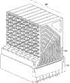
根据图55-63描述了高速底板连接器系统400的又一实施方式。通常,连接器系统400包括接地屏蔽件402、多个壳体段404以及多个电触头组件406。在一些实施方式中,接地屏蔽件402可包括液晶聚合物、锡(Sn)镀层和铜(Cu)镀层。然而,在其他实施方式中,接地屏蔽件402可包括其他材料,例如锌(Zn)、铝(Al)或者导电聚合物。Yet another embodiment of a high-speed
参照图57A和57B,多个电触头组件406中的每个电触头组件408包括多个电触头410和多个基本刚性的绝缘部分412。在一些实施方式中,电触头410可包括磷青铜基材料以及在镍镀层之上的金镀层和锡镀层,并且绝缘部分412可包括液晶聚合物(LCP)。然而,在其他实施方式中,电触头410可包括其他导电的基体材料以及镀层(贵金属或非贵金属),并且绝缘部分412可包括其他聚合物。Referring to FIGS. 57A and 57B , each electrical contact assembly 408 of the plurality of electrical contact assemblies 406 includes a plurality of electrical contacts 410 and a plurality of substantially rigid insulating portions 412 . In some embodiments, the electrical contacts 410 may include a phosphor bronze-based material with gold and tin plating over a nickel plating, and the insulating portion 412 may include a liquid crystal polymer (LCP). However, in other embodiments, the electrical contacts 410 may include other conductive base materials and platings (noble or non-noble), and the insulating portion 412 may include other polymers.
多个电触头410中的每个电触头在电触头的安装端426处限定了具有一个或多个基片接合元件415例如电触头安装管脚的长度方向414,并且在电触头的配合端422处限定了电配合连接器417。在一些实施方式中,电配合连接器417是如图8所示的封闭带形,而在其他实施方式中,电配合连接器417是如图9A所示的三条板形或者如图9B所示的双条板形。其他的配合连接器形式可以具有多个条板。Each of the plurality of electrical contacts 410 defines a lengthwise direction 414 having one or more
将电触头410定位在电触头组件408中,以使每个电触头与另一个电触头基本上平行。典型地,多个电触头410中的两个电触头形成了电触头对430,在一些实施方式中,电触头对430可以是差分对。The electrical contacts 410 are positioned in the electrical contact assembly 408 such that each electrical contact is substantially parallel to the other electrical contact. Typically, two of the plurality of electrical contacts 410 form an
沿多个电触头410的长度方向定位多个绝缘部分412以使电触头410以基本平行的关系定位。多个绝缘部分412沿多个电触头410的长度彼此分隔。由于绝缘部分之间的间隔416,可以在绝缘部分412之间弯曲电触头组件408,如图55B所示,同时仍然在多个电触头410的电触头之间保持基本平行的关系。平行的触头对可以在每个绝缘部分中以螺旋状的构造(像卷绕的导线对)定位,并且被有利地取向以用于在绝缘部分之间的间隔处弯曲。The plurality of insulating portions 412 are positioned along the length of the plurality of electrical contacts 410 such that the electrical contacts 410 are positioned in a substantially parallel relationship. The plurality of insulating portions 412 are separated from each other along the length of the plurality of electrical contacts 410 . Due to the spacing 416 between the insulating portions, the electrical contact assembly 408 may be bent between the insulating portions 412, as shown in FIG. 55B, while still maintaining a substantially parallel relationship between the electrical contacts of the plurality of electrical contacts 410. Parallel pairs of contacts may be positioned in each insulating section in a helical configuration (like a coiled pair of wires), and are advantageously oriented for bending at the spaces between the insulating sections.
多个壳体段404中的每个壳体段限定了多个电触头通道418。电触头通道418可包括导电表面以产生导电路径。每个电触头通道418适于接收电触头组件408中的一个并将定位在电触头通道中的电触头组件的电触头410与电触头通道的导电表面和定位在其他电触头通道中的电触头410电隔离。Each housing segment in plurality of
如图56A和56C所示,接地屏蔽件402限定了多段通道425,每段通道425适于接收多个壳体段404的壳体段。接地屏蔽件402定位多个壳体段404,如图55所示,从而使从壳体段404延伸的电触头组件406的电配合连接器417形成行和列的矩阵。应该明白,多个壳体段404中的每个壳体段以及结合的电触头组件406形成了矩阵的行,从而当多个壳体段404彼此相邻定位时,如图54B所示,形成了矩阵。As shown in FIGS. 56A and 56C , the
接地屏蔽件402限定了从接地屏蔽件402的配合端422延伸的多个接地配合片420,并且限定了从接地屏蔽件402的安装端426延伸的多个基片接合元件424,例如接地安装管脚。接地安装管脚可以限定宽边和比宽边小的边缘。The
在一些实施方式中,对应于电触头对430的每对电触头安装管脚415被定位在两个取向中的一个取向上,例如耦合的宽边或耦合的边缘。在其他实施方式中,对应于电触头对430的每对电触头安装管脚415被定位在两个取向中的一个取向上,其中在第一取向,对齐一对电触头安装管脚415从而使管脚的宽边基本与基片平行,而在第二取向,对齐一对电触头安装管脚415从而使宽边基本垂直于基片。在宽边和边缘之间从0度到90度的其他安装管脚取向是可能的。而且,电触头安装管脚415和接地安装管脚424可被定位为以产生除噪印迹,如上面关于图26、27和28所述。In some embodiments, each pair of electrical
连接器系统400可包括安装端组织器428和/或配合端组织器432。在一些实施方式中,安装端和配合端组织器428、432可包括液晶聚合物(LCP)。然而,在其他实施方式中,安装端和配合端组织器428、432可包括其他聚合物。安装端组织器428限定了多个通孔434,从而当把安装端组织器428定位在接地屏蔽件402的安装端426时,从接地屏蔽件402延伸的接地安装管脚424以及从多个电触头组件406延伸的电触头安装管脚415穿过多个通孔434,并且远离安装端组织器428延伸以接合底板电路板或子卡电路板中的一个,如上所述。
类似地,配合端组织器432限定了多个通孔435,从而当把配合端组织器432定位在接地屏蔽件402的配合端426时,从接地屏蔽件402延伸的接地配合片402以及从多个电触头组件406延伸的电配合连接器417穿过多个通孔434,并且远离配合端组织器432延伸。Similarly,
参照图62,连接器系统400包括端接头模块436,例如上述的端接头模块136、236、336,其适于接收接地配合片420以及远离配合端组织器432延伸的电配合连接器417。当端接头模块436接收电配合连接器417时,从端接头模块436的配合面延伸的多个信号管脚对442接合电配合连接器417。类似地,当端接头模块436接收接地配合片420时,从端接头模块436的配合面延伸的多个C型接地屏蔽件438和一行接地片440接合接地配合片420。Referring to FIG. 62 , the
图63A、63B、63C和63D是示出了上面关于图55-62所述的电连接器系统的近似特性的曲线图。图63A是示出了电连接器系统的插入损耗对频率的特性能图;图63B是示出了电连接器系统的回程损耗对频率的特性图;图63C是示出了电连接器系统的近端串扰噪声对频率的特性图;以及图63D是示出了电连接器系统的远端串扰噪声对频率的特性图。如图63A、63B、63C和63D所示,电连接器系统给在以高达至少25Gbps的速度操作的第一和第二电触头阵列410的电触头上负载的电信号提供了大致相同的阻抗分布图。63A, 63B, 63C and 63D are graphs showing approximate characteristics of the electrical connector system described above with respect to FIGS. 55-62. Figure 63 A is a characteristic graph showing the insertion loss of the electrical connector system versus frequency; Figure 63B is a characteristic graph showing the return loss of the electrical connector system versus frequency; Figure 63C is a graph showing the frequency of the electrical connector system NEXT noise vs. frequency characteristic plot; and FIG. 63D is a plot showing FEXT noise vs. frequency for an electrical connector system. As shown in Figures 63A, 63B, 63C, and 63D, the electrical connector system provides substantially the same electrical signals carried on the electrical contacts of the first and second electrical contact arrays 410 operating at speeds up to at least 25 Gbps. Impedance distribution map.
下面根据图64-71描述了在高速底板连接器系统中使用的薄片组件的其他实施方式。类似于上面关于图2-54所述的连接器系统100、200、300,高速底板连接器系统可包括通过薄片壳体在连接器系统500中彼此相邻定位的多个薄片组件502,如上所述。Other embodiments of wafer assemblies for use in high-speed backplane connector systems are described below with respect to FIGS. 64-71. Similar to the
参照图64和65,在一个实施方式中,多个薄片组件502中的每个薄片组件505包括多个电信号触头506、多个可接地的电触头508以及框架510。框架510限定了第一侧512和第二侧514。第一侧512还限定了多个第一通道516,每个第一通道516包括导电表面并且适于接收多个电信号触头506中的一个或多个电信号触头。在一些实施方式中,将多个电信号触头506定位在信号引线外壳518中,信号引线外壳518的大小适合被多个第一通道516接收,如图64所示。将认识到,在一些实施方式中,将多个电信号触头506中的两个电信号触头定位在信号引线外壳518中以形成电触头对520,电触头对520还可以是差分对。Referring to FIGS. 64 and 65 , in one embodiment, each
框架510的第二侧514也可以限定多个第二通道522。多个第二通道522中的每个通道包括导电表面并且适于接收一个或多个电信号触头,如下面更详细的解释。The
框架510还包括延伸到多个第一通道516的导电表面中的多个通孔524。在一些实施方式中,多个通孔524还可以延伸到多个第二通道522的导电表面中。
如图64所示,多个通孔524中的每个通孔沿框架510与多个通孔中的另一个通孔分开,并且位于多个第一通道516的通道之间的框架510上。多个通孔524中的每个通孔适于接收多个可接地电触头508中的可接地电触头。在一些实施方式中,将多个可接地的电触头508电连接到第一和第二侧512、514的导电表面。As shown in FIG. 64 , each of the plurality of through-
薄片壳体,例如上面所述的薄片壳体104、204和304,接收多个薄片组件502的配合端526,并使每个薄片组件与多个薄片组件502中的另一个薄片组件相邻定位。当定位在薄片壳体504中时,接合框架510的第一侧514的信号引线外壳518也接合相邻薄片组件的框架510的第二侧514。A wafer housing, such as
如图66A、66B和67所示,连接器系统500包括适于与薄片壳体和多个薄片组件502配合的端接头单元536。当端接头单元536与薄片壳体和多个薄片组件502配合时,薄片组件502的电信号触头506接收从端接头单元536的配合面延伸的多个信号管脚对542。类似地,当端接头单元536与薄片壳体和多个薄片组件502配合时,可接地的电触头508接收从端接头模块536的配合面延伸的多个接地管脚或接地屏蔽件540。As shown in FIGS. 66A , 66B and 67 , the connector system 500 includes a termination unit 536 adapted to mate with the wafer housing and the plurality of
信号管脚对542中的每个信号管脚限定了基片接合元件,例如信号安装管脚544,并且每个接地管脚540限定了基片接合元件,例如接地安装管脚546。信号管脚542和接地管脚540延伸过端接头单元536,从而使信号安装管脚544和接地安装管脚546远离端接头模块536的安装面延伸以接合底板电路板或子卡电路板。Each signal pin of
如上所述,在一些实施方式中,每对信号安装管脚544被定位在两个取向中的一个取向上,例如耦合的宽边或耦合的边缘。在其他实施方式中,每对信号安装管脚544被定位在两个取向中的一个取向上,其中在第一取向,对齐一对信号安装管脚544从而使该对的宽边基本平行于基片,和在第二取向,对齐一对信号安装管脚544从而使该对的宽边基本垂直于基片。而且,可以定位信号安装管脚544和接地安装管脚546以产生除噪印迹,如上面关于图26、27和28所述。As noted above, in some embodiments, each pair of signal mounting pins 544 is positioned in one of two orientations, such as coupled broadside or coupled edge. In other embodiments, each pair of signal mounting pins 544 is positioned in one of two orientations, wherein in the first orientation, a pair of signal mounting pins 544 are aligned such that the broad sides of the pair are substantially parallel to the base. chip, and in the second orientation, align the pair of signal mounting pins 544 so that the broadsides of the pair are substantially perpendicular to the substrate. Also, the signal mounting pin 544 and the ground mounting pin 546 may be positioned to create a noise canceling footprint, as described above with respect to FIGS. 26 , 27 and 28 .
参照图68,在一些实施方式中,电信号触头没有嵌入在信号引线外壳518中,而是定位在信号引线外壳518的通道中。例如,信号引线外壳518可以限定多个第一通道525和多个第二通道526。将第一电触头阵列527定位在多个第一通道525中,并且将第二电触头阵列528定位在多个第二通道526中。Referring to FIG. 68 , in some embodiments, the electrical signal contacts are not embedded in the signal
当定位在通道525、526中时,第一电触头阵列527中的每个电触头与第二电触头阵列528的电触头相邻定位。两个电触头共同形成电触头对520,其也可以是差分对。When positioned in the
当把信号引线外壳518定位在薄片组件的框架510和相邻薄片组件的框架510之间时,在信号引线外壳518的通道525、526之一与薄片组件505的框架510之间形成了多个气隙529。气隙529用于将位于气隙中的电触头与通道525、526的导电表面电隔离。When the signal
参照图69和70,在一些实施方式中,每个薄片组件505可包括锁定组件532以将多个薄片组件502固定在一起。例如,如图68所示,锁定组件532可以是延伸到相邻薄片组件505中并与相邻薄片组件505的框架510配合的叉状部件。可替换地,如图69所示,锁定组件532可以是接合两个相邻薄片组件505的波纹状弹簧。69 and 70, in some embodiments, each
图71A、71B、71C和71D是示出了利用上面关于图64-70所述的薄片组件的高速连接器系统的近似特性的曲线图。图71A是示出了高速连接器系统的插入损耗对频率的特性图;图71B是示出了高速连接器系统的回程损耗对频率的特性图;图71C是示出了高速连接器系统的近端串扰噪声对频率的特性图;以及图71D是示出了高速连接器系统的远端串扰噪声对频率的特性图。如图71A、71B、71C和71D所示,电连接器系统给在以高达至少25Gbps的速度操作的电触头506上负载的电信号提供了大致相同的阻抗分布图。71A, 71B, 71C, and 71D are graphs showing approximate characteristics of a high-speed connector system utilizing the wafer assembly described above with respect to FIGS. 64-70. 71A is a characteristic diagram showing the insertion loss of the high-speed connector system versus frequency; FIG. 71B is a characteristic diagram showing the return loss of the high-speed connector system versus frequency; FIG. Figure 71D is a characteristic diagram showing far-end crosstalk noise versus frequency for a high-speed connector system. As shown in FIGS. 71A, 71B, 71C, and 71D, the electrical connector system provides substantially the same impedance profile for electrical signals loaded on
Claims (8)
Translated fromChineseApplications Claiming Priority (6)
| Application Number | Priority Date | Filing Date | Title |
|---|---|---|---|
| US20095508P | 2008-12-05 | 2008-12-05 | |
| US61/200,955 | 2008-12-05 | ||
| US20519409P | 2009-01-16 | 2009-01-16 | |
| US61/205,194 | 2009-01-16 | ||
| US12/474,674US7927143B2 (en) | 2008-12-05 | 2009-05-29 | Electrical connector system |
| US12/474,674 | 2009-05-29 |
Publications (2)
| Publication Number | Publication Date |
|---|---|
| CN101783449Atrue CN101783449A (en) | 2010-07-21 |
| CN101783449B CN101783449B (en) | 2014-01-29 |
Family
ID=41667290
Family Applications (1)
| Application Number | Title | Priority Date | Filing Date |
|---|---|---|---|
| CN200911000191.7AActiveCN101783449B (en) | 2008-12-05 | 2009-12-07 | Electrical Connector System |
Country Status (4)
| Country | Link |
|---|---|
| US (1) | US7927143B2 (en) |
| EP (1) | EP2194609B1 (en) |
| CN (1) | CN101783449B (en) |
| TW (1) | TWI519002B (en) |
Cited By (20)
| Publication number | Priority date | Publication date | Assignee | Title |
|---|---|---|---|---|
| CN102185196A (en)* | 2009-12-29 | 2011-09-14 | 泰科电子公司 | Electrical connector system |
| CN103296546A (en)* | 2012-02-22 | 2013-09-11 | 富士康(昆山)电脑接插件有限公司 | Electric coupler assembly |
| US8961229B2 (en) | 2012-02-22 | 2015-02-24 | Hon Hai Precision Industry Co., Ltd. | High speed high density connector assembly |
| CN104718666A (en)* | 2012-08-27 | 2015-06-17 | 富加宜(亚洲)私人有限公司 | High speed electrical connector |
| CN105098446A (en)* | 2014-04-22 | 2015-11-25 | 泰科电子公司 | Interlayer type plug connector |
| CN106469863A (en)* | 2015-08-20 | 2017-03-01 | 莫列斯公司 | Electrical connectors and electrical connection devices |
| CN108011254A (en)* | 2016-10-31 | 2018-05-08 | 泰连公司 | The electric connector of ground shield with the impedance at control mating interface |
| CN108432065A (en)* | 2015-12-07 | 2018-08-21 | 安费诺富加宜(亚洲)私人有限公司 | With the electrical electrical cnnector for sharing ground connection |
| CN108695651A (en)* | 2017-04-07 | 2018-10-23 | 泰连公司 | Connector assembly with pin organizer |
| CN109256639A (en)* | 2017-07-13 | 2019-01-22 | 泰连公司 | Connector assembly with pin organizer |
| CN109728456A (en)* | 2017-10-27 | 2019-05-07 | 泰连公司 | Connector Assemblies with Conductive Pads |
| CN110088985A (en)* | 2016-10-19 | 2019-08-02 | 安费诺有限公司 | Flexible shield for ultra-high speed high density electrical interconnects |
| CN110098509A (en)* | 2018-01-30 | 2019-08-06 | 泰连公司 | Electric connector system with pin connector |
| CN110459919A (en)* | 2018-06-29 | 2019-11-15 | 中航光电科技股份有限公司 | Differential connector and its differential pair shielding structure, shielding buckle plate |
| CN111641083A (en)* | 2014-11-12 | 2020-09-08 | 安费诺有限公司 | Very high speed, high density electrical interconnect system with impedance control in the mating region |
| US11444398B2 (en) | 2018-03-22 | 2022-09-13 | Amphenol Corporation | High density electrical connector |
| US11469553B2 (en) | 2020-01-27 | 2022-10-11 | Fci Usa Llc | High speed connector |
| US11742620B2 (en) | 2018-11-21 | 2023-08-29 | Amphenol Corporation | High-frequency electrical connector |
| US11799246B2 (en) | 2020-01-27 | 2023-10-24 | Fci Usa Llc | High speed connector |
| USD1002553S1 (en) | 2021-11-03 | 2023-10-24 | Amphenol Corporation | Gasket for connector |
Families Citing this family (35)
| Publication number | Priority date | Publication date | Assignee | Title |
|---|---|---|---|---|
| US20090291593A1 (en)* | 2005-06-30 | 2009-11-26 | Prescott Atkinson | High frequency broadside-coupled electrical connector |
| WO2010038110A1 (en)* | 2008-09-30 | 2010-04-08 | Fci | Lead frame assembly for an electrical connector |
| CN107069274B (en) | 2010-05-07 | 2020-08-18 | 安费诺有限公司 | High performance cable connector |
| US8690604B2 (en) | 2011-10-19 | 2014-04-08 | Tyco Electronics Corporation | Receptacle assembly |
| US8398431B1 (en)* | 2011-10-24 | 2013-03-19 | Tyco Electronics Corporation | Receptacle assembly |
| US8398432B1 (en)* | 2011-11-07 | 2013-03-19 | Tyco Electronics Corporation | Grounding structures for header and receptacle assemblies |
| US8500487B2 (en)* | 2011-11-15 | 2013-08-06 | Tyco Electronics Corporation | Grounding structures for header and receptacle assemblies |
| US8449330B1 (en)* | 2011-12-08 | 2013-05-28 | Tyco Electronics Corporation | Cable header connector |
| US9240644B2 (en) | 2012-08-22 | 2016-01-19 | Amphenol Corporation | High-frequency electrical connector |
| US20140194004A1 (en)* | 2013-01-07 | 2014-07-10 | Tyco Electronics Corporation | Grounding structures for a receptacle assembly |
| US9142896B2 (en) | 2013-11-15 | 2015-09-22 | Tyco Electronics Corporation | Connector assemblies having pin spacers with lugs |
| CN115411547A (en) | 2014-01-22 | 2022-11-29 | 安费诺有限公司 | Electrical connector, subassembly, module, cable assembly, electrical assembly and circuit board |
| US9099813B1 (en) | 2014-02-28 | 2015-08-04 | Tyco Electronics Corporation | Electrical connector assembly having a contact organizer |
| US9281579B2 (en)* | 2014-05-13 | 2016-03-08 | Tyco Electronics Corporation | Electrical connectors having leadframes |
| CN108701922B (en) | 2015-07-07 | 2020-02-14 | Afci亚洲私人有限公司 | Electrical connector |
| TWI754439B (en) | 2015-07-23 | 2022-02-01 | 美商安芬諾Tcs公司 | Connector, method of manufacturing connector, extender module for connector, and electric system |
| US10453795B2 (en)* | 2015-12-26 | 2019-10-22 | Intel Corporation | Microprocessor package with first level die bump ground webbing structure |
| WO2017201170A1 (en) | 2016-05-18 | 2017-11-23 | Amphenol Corporation | Controlled impedance edged coupled connectors |
| TWI746561B (en) | 2016-05-31 | 2021-11-21 | 美商安芬諾股份有限公司 | High performance cable termination |
| CN112151987B (en) | 2016-08-23 | 2022-12-30 | 安费诺有限公司 | Configurable high performance connector |
| TWI788394B (en) | 2017-08-03 | 2023-01-01 | 美商安芬諾股份有限公司 | Cable assembly and method of manufacturing the same |
| WO2019195319A1 (en) | 2018-04-02 | 2019-10-10 | Ardent Concepts, Inc. | Controlled-impedance compliant cable termination |
| CN208862209U (en) | 2018-09-26 | 2019-05-14 | 安费诺东亚电子科技(深圳)有限公司 | A connector and its applied PCB board |
| US11101611B2 (en) | 2019-01-25 | 2021-08-24 | Fci Usa Llc | I/O connector configured for cabled connection to the midboard |
| WO2020154507A1 (en) | 2019-01-25 | 2020-07-30 | Fci Usa Llc | I/o connector configured for cable connection to a midboard |
| CN111585098B (en) | 2019-02-19 | 2025-08-19 | 安费诺有限公司 | High-speed connector |
| WO2020172395A1 (en) | 2019-02-22 | 2020-08-27 | Amphenol Corporation | High performance cable connector assembly |
| TW202448032A (en) | 2019-05-20 | 2024-12-01 | 美商安芬諾股份有限公司 | Connector module, connector, electronic assembly, electrical connector and wafer of connector module |
| CN114788097A (en) | 2019-09-19 | 2022-07-22 | 安费诺有限公司 | High speed electronic system with midplane cable connector |
| CN113258325A (en) | 2020-01-28 | 2021-08-13 | 富加宜(美国)有限责任公司 | High-frequency middle plate connector |
| CN215816516U (en) | 2020-09-22 | 2022-02-11 | 安费诺商用电子产品(成都)有限公司 | Electrical connector |
| CN213636403U (en) | 2020-09-25 | 2021-07-06 | 安费诺商用电子产品(成都)有限公司 | Electrical connector |
| CN215266741U (en) | 2021-08-13 | 2021-12-21 | 安费诺商用电子产品(成都)有限公司 | High-performance card connector meeting high-bandwidth transmission |
| USD1067191S1 (en) | 2021-12-14 | 2025-03-18 | Amphenol Corporation | Electrical connector |
| USD1068685S1 (en) | 2021-12-14 | 2025-04-01 | Amphenol Corporation | Electrical connector |
Citations (4)
| Publication number | Priority date | Publication date | Assignee | Title |
|---|---|---|---|---|
| US5795191A (en)* | 1996-09-11 | 1998-08-18 | Preputnick; George | Connector assembly with shielded modules and method of making same |
| WO2001057963A2 (en)* | 2000-02-03 | 2001-08-09 | Teradyne, Inc. | High speed pressure mount connector |
| US20060281346A1 (en)* | 2005-06-10 | 2006-12-14 | Hon Hai Precision Ind.Co.,Ltd | Backplane connector |
| US7309257B1 (en)* | 2006-06-30 | 2007-12-18 | Fci Americas Technology, Inc. | Hinged leadframe assembly for an electrical connector |
Family Cites Families (14)
| Publication number | Priority date | Publication date | Assignee | Title |
|---|---|---|---|---|
| US5882227A (en)* | 1997-09-17 | 1999-03-16 | Intercon Systems, Inc. | Controlled impedance connector block |
| US6824391B2 (en)* | 2000-02-03 | 2004-11-30 | Tyco Electronics Corporation | Electrical connector having customizable circuit board wafers |
| KR20020073527A (en)* | 2000-02-03 | 2002-09-26 | 테라다인 인코퍼레이티드 | Connector with shielding |
| EP1284032B1 (en)* | 2000-05-25 | 2008-12-03 | Tyco Electronics Corporation | Electrical connector having contacts isolated by shields |
| US20030022555A1 (en)* | 2001-03-30 | 2003-01-30 | Samtec, Inc. | Ground plane shielding array |
| US6899566B2 (en)* | 2002-01-28 | 2005-05-31 | Erni Elektroapparate Gmbh | Connector assembly interface for L-shaped ground shields and differential contact pairs |
| US6709294B1 (en)* | 2002-12-17 | 2004-03-23 | Teradyne, Inc. | Electrical connector with conductive plastic features |
| US6932626B2 (en)* | 2003-06-30 | 2005-08-23 | Tyco Electronics Corporation | Electrical card connector |
| JP2005032529A (en)* | 2003-07-10 | 2005-02-03 | Jst Mfg Co Ltd | High-speed transmission connector |
| US7217889B1 (en)* | 2003-12-04 | 2007-05-15 | Cisco Technology, Inc. | System and method for reducing crosstalk between vias in a printed circuit board |
| JP3909769B2 (en)* | 2004-01-09 | 2007-04-25 | 日本航空電子工業株式会社 | connector |
| US7371117B2 (en)* | 2004-09-30 | 2008-05-13 | Amphenol Corporation | High speed, high density electrical connector |
| US7207807B2 (en)* | 2004-12-02 | 2007-04-24 | Tyco Electronics Corporation | Noise canceling differential connector and footprint |
| US7163421B1 (en)* | 2005-06-30 | 2007-01-16 | Amphenol Corporation | High speed high density electrical connector |
- 2009
- 2009-05-29USUS12/474,674patent/US7927143B2/enactiveActive
- 2009-12-03TWTW098141336Apatent/TWI519002B/enactive
- 2009-12-04EPEP09178066.8Apatent/EP2194609B1/enactiveActive
- 2009-12-07CNCN200911000191.7Apatent/CN101783449B/enactiveActive
Patent Citations (4)
| Publication number | Priority date | Publication date | Assignee | Title |
|---|---|---|---|---|
| US5795191A (en)* | 1996-09-11 | 1998-08-18 | Preputnick; George | Connector assembly with shielded modules and method of making same |
| WO2001057963A2 (en)* | 2000-02-03 | 2001-08-09 | Teradyne, Inc. | High speed pressure mount connector |
| US20060281346A1 (en)* | 2005-06-10 | 2006-12-14 | Hon Hai Precision Ind.Co.,Ltd | Backplane connector |
| US7309257B1 (en)* | 2006-06-30 | 2007-12-18 | Fci Americas Technology, Inc. | Hinged leadframe assembly for an electrical connector |
Cited By (43)
| Publication number | Priority date | Publication date | Assignee | Title |
|---|---|---|---|---|
| CN102185196B (en)* | 2009-12-29 | 2015-02-04 | 泰科电子公司 | Electrical connector system |
| CN102185196A (en)* | 2009-12-29 | 2011-09-14 | 泰科电子公司 | Electrical connector system |
| CN103296546A (en)* | 2012-02-22 | 2013-09-11 | 富士康(昆山)电脑接插件有限公司 | Electric coupler assembly |
| US8961229B2 (en) | 2012-02-22 | 2015-02-24 | Hon Hai Precision Industry Co., Ltd. | High speed high density connector assembly |
| US9160114B2 (en) | 2012-02-22 | 2015-10-13 | Hon Hai Precision Industry Co., Ltd. | High speed high density connector assembly |
| CN103296546B (en)* | 2012-02-22 | 2015-11-25 | 富士康(昆山)电脑接插件有限公司 | Electric coupler component |
| CN104718666B (en)* | 2012-08-27 | 2018-08-10 | 安费诺富加宜(亚洲)私人有限公司 | High Speed Electrical Connector |
| CN104718666A (en)* | 2012-08-27 | 2015-06-17 | 富加宜(亚洲)私人有限公司 | High speed electrical connector |
| CN109004398B (en)* | 2012-08-27 | 2021-09-07 | 安费诺富加宜(亚洲)私人有限公司 | High speed electrical connector |
| CN109004398A (en)* | 2012-08-27 | 2018-12-14 | 安费诺富加宜(亚洲)私人有限公司 | High-speed electrical connectors |
| CN105098446A (en)* | 2014-04-22 | 2015-11-25 | 泰科电子公司 | Interlayer type plug connector |
| CN105098446B (en)* | 2014-04-22 | 2019-03-12 | 泰连公司 | Mezzanine Plug Connector |
| CN111641083A (en)* | 2014-11-12 | 2020-09-08 | 安费诺有限公司 | Very high speed, high density electrical interconnect system with impedance control in the mating region |
| US11764523B2 (en) | 2014-11-12 | 2023-09-19 | Amphenol Corporation | Very high speed, high density electrical interconnection system with impedance control in mating region |
| CN106469863A (en)* | 2015-08-20 | 2017-03-01 | 莫列斯公司 | Electrical connectors and electrical connection devices |
| CN106469863B (en)* | 2015-08-20 | 2018-10-09 | 莫列斯公司 | Electric connector and electric connecting device |
| CN108432065A (en)* | 2015-12-07 | 2018-08-21 | 安费诺富加宜(亚洲)私人有限公司 | With the electrical electrical cnnector for sharing ground connection |
| US11245229B2 (en) | 2015-12-07 | 2022-02-08 | Fci Usa Llc | Electrical connector having electrically commoned grounds |
| CN108432065B (en)* | 2015-12-07 | 2021-04-23 | 安费诺富加宜(亚洲)私人有限公司 | Electrical connector with electrically common ground |
| CN115189188A (en)* | 2016-10-19 | 2022-10-14 | 安费诺有限公司 | Flexible shielding piece, electric connector and electronic device |
| US11387609B2 (en) | 2016-10-19 | 2022-07-12 | Amphenol Corporation | Compliant shield for very high speed, high density electrical interconnection |
| CN110088985A (en)* | 2016-10-19 | 2019-08-02 | 安费诺有限公司 | Flexible shield for ultra-high speed high density electrical interconnects |
| CN110088985B (en)* | 2016-10-19 | 2022-07-05 | 安费诺有限公司 | Flexible shield for ultra-high speed high density electrical interconnects |
| TWI797094B (en)* | 2016-10-19 | 2023-04-01 | 美商安芬諾股份有限公司 | Compliant shield for very high speed, high density electrical interconnection |
| CN108011254B (en)* | 2016-10-31 | 2020-10-23 | 泰连公司 | Electrical connector having a ground shield controlling impedance at a mating interface |
| CN108011254A (en)* | 2016-10-31 | 2018-05-08 | 泰连公司 | The electric connector of ground shield with the impedance at control mating interface |
| CN108695651A (en)* | 2017-04-07 | 2018-10-23 | 泰连公司 | Connector assembly with pin organizer |
| CN109256639A (en)* | 2017-07-13 | 2019-01-22 | 泰连公司 | Connector assembly with pin organizer |
| CN109728456B (en)* | 2017-10-27 | 2022-07-05 | 泰连公司 | Connector Assemblies with Conductive Pads |
| CN109728456A (en)* | 2017-10-27 | 2019-05-07 | 泰连公司 | Connector Assemblies with Conductive Pads |
| CN110098509A (en)* | 2018-01-30 | 2019-08-06 | 泰连公司 | Electric connector system with pin connector |
| US11444398B2 (en) | 2018-03-22 | 2022-09-13 | Amphenol Corporation | High density electrical connector |
| CN110459919B (en)* | 2018-06-29 | 2022-01-25 | 中航光电科技股份有限公司 | Differential connector and differential pair shielding structure and shielding buckle plate thereof |
| CN110459919A (en)* | 2018-06-29 | 2019-11-15 | 中航光电科技股份有限公司 | Differential connector and its differential pair shielding structure, shielding buckle plate |
| US11742620B2 (en) | 2018-11-21 | 2023-08-29 | Amphenol Corporation | High-frequency electrical connector |
| US12218462B2 (en) | 2018-11-21 | 2025-02-04 | Amphenol Corporation | High-frequency electrical connector |
| US11469554B2 (en) | 2020-01-27 | 2022-10-11 | Fci Usa Llc | High speed, high density direct mate orthogonal connector |
| US11469553B2 (en) | 2020-01-27 | 2022-10-11 | Fci Usa Llc | High speed connector |
| US11799246B2 (en) | 2020-01-27 | 2023-10-24 | Fci Usa Llc | High speed connector |
| US11817657B2 (en) | 2020-01-27 | 2023-11-14 | Fci Usa Llc | High speed, high density direct mate orthogonal connector |
| US12074398B2 (en) | 2020-01-27 | 2024-08-27 | Fci Usa Llc | High speed connector |
| US12341302B2 (en) | 2020-01-27 | 2025-06-24 | Fci Usa Llc | High speed connector |
| USD1002553S1 (en) | 2021-11-03 | 2023-10-24 | Amphenol Corporation | Gasket for connector |
Also Published As
| Publication number | Publication date |
|---|---|
| US20100144175A1 (en) | 2010-06-10 |
| CN101783449B (en) | 2014-01-29 |
| TWI519002B (en) | 2016-01-21 |
| EP2194609B1 (en) | 2014-07-02 |
| TW201031055A (en) | 2010-08-16 |
| US7927143B2 (en) | 2011-04-19 |
| EP2194609A1 (en) | 2010-06-09 |
Similar Documents
| Publication | Publication Date | Title |
|---|---|---|
| CN101888032B (en) | Electrical connector system | |
| CN101783450B (en) | Electrical connector system | |
| CN101958474B (en) | Electrical connector system. | |
| CN101958473B (en) | Termination head assembly for electric connector to be installed to substrate | |
| CN101783449A (en) | Electrical Connector System | |
| EP2194607B1 (en) | Electrical connector system | |
| US7775802B2 (en) | Electrical connector system | |
| US7976318B2 (en) | Electrical connector system | |
| EP1026930B1 (en) | Circuit board side interconnect |
Legal Events
| Date | Code | Title | Description |
|---|---|---|---|
| C06 | Publication | ||
| PB01 | Publication | ||
| C10 | Entry into substantive examination | ||
| SE01 | Entry into force of request for substantive examination | ||
| C14 | Grant of patent or utility model | ||
| GR01 | Patent grant | ||
| CP01 | Change in the name or title of a patent holder | Address after:American Pennsylvania Patentee after:TE CONNECTIVITY Corp. Address before:American Pennsylvania Patentee before:Tyco Electronics Corp. | |
| CP01 | Change in the name or title of a patent holder | ||
| TR01 | Transfer of patent right | Effective date of registration:20250718 Address after:Schaffhausen Patentee after:Tailian Service Co.,Ltd. Country or region after:Switzerland Address before:Pennsylvania, USA Patentee before:TE CONNECTIVITY Corp. Country or region before:U.S.A. | |
| TR01 | Transfer of patent right | ||
| TR01 | Transfer of patent right | Effective date of registration:20250905 Address after:Schaffhausen Patentee after:Tailian solutions Co.,Ltd. Country or region after:Switzerland Address before:Schaffhausen Patentee before:Tailian Service Co.,Ltd. Country or region before:Switzerland | |
| TR01 | Transfer of patent right |