CN101779287A - Resistance change nonvolatile memory device - Google Patents
Resistance change nonvolatile memory deviceDownload PDFInfo
- Publication number
- CN101779287A CN101779287ACN200880025595.9ACN200880025595ACN101779287ACN 101779287 ACN101779287 ACN 101779287ACN 200880025595 ACN200880025595 ACN 200880025595ACN 101779287 ACN101779287 ACN 101779287A
- Authority
- CN
- China
- Prior art keywords
- electrode
- voltage
- resistance
- memory device
- resistance change
- Prior art date
- Legal status (The legal status is an assumption and is not a legal conclusion. Google has not performed a legal analysis and makes no representation as to the accuracy of the status listed.)
- Granted
Links
Images


Classifications
- G—PHYSICS
- G11—INFORMATION STORAGE
- G11C—STATIC STORES
- G11C13/00—Digital stores characterised by the use of storage elements not covered by groups G11C11/00, G11C23/00, or G11C25/00
- G11C13/0002—Digital stores characterised by the use of storage elements not covered by groups G11C11/00, G11C23/00, or G11C25/00 using resistive RAM [RRAM] elements
- G11C13/0007—Digital stores characterised by the use of storage elements not covered by groups G11C11/00, G11C23/00, or G11C25/00 using resistive RAM [RRAM] elements comprising metal oxide memory material, e.g. perovskites
- H—ELECTRICITY
- H10—SEMICONDUCTOR DEVICES; ELECTRIC SOLID-STATE DEVICES NOT OTHERWISE PROVIDED FOR
- H10B—ELECTRONIC MEMORY DEVICES
- H10B63/00—Resistance change memory devices, e.g. resistive RAM [ReRAM] devices
- H10B63/30—Resistance change memory devices, e.g. resistive RAM [ReRAM] devices comprising selection components having three or more electrodes, e.g. transistors
- H—ELECTRICITY
- H10—SEMICONDUCTOR DEVICES; ELECTRIC SOLID-STATE DEVICES NOT OTHERWISE PROVIDED FOR
- H10N—ELECTRIC SOLID-STATE DEVICES NOT OTHERWISE PROVIDED FOR
- H10N70/00—Solid-state devices having no potential barriers, and specially adapted for rectifying, amplifying, oscillating or switching
- H10N70/011—Manufacture or treatment of multistable switching devices
- H10N70/021—Formation of switching materials, e.g. deposition of layers
- H10N70/026—Formation of switching materials, e.g. deposition of layers by physical vapor deposition, e.g. sputtering
- H—ELECTRICITY
- H10—SEMICONDUCTOR DEVICES; ELECTRIC SOLID-STATE DEVICES NOT OTHERWISE PROVIDED FOR
- H10N—ELECTRIC SOLID-STATE DEVICES NOT OTHERWISE PROVIDED FOR
- H10N70/00—Solid-state devices having no potential barriers, and specially adapted for rectifying, amplifying, oscillating or switching
- H10N70/20—Multistable switching devices, e.g. memristors
- H10N70/24—Multistable switching devices, e.g. memristors based on migration or redistribution of ionic species, e.g. anions, vacancies
- H—ELECTRICITY
- H10—SEMICONDUCTOR DEVICES; ELECTRIC SOLID-STATE DEVICES NOT OTHERWISE PROVIDED FOR
- H10N—ELECTRIC SOLID-STATE DEVICES NOT OTHERWISE PROVIDED FOR
- H10N70/00—Solid-state devices having no potential barriers, and specially adapted for rectifying, amplifying, oscillating or switching
- H10N70/801—Constructional details of multistable switching devices
- H10N70/821—Device geometry
- H10N70/826—Device geometry adapted for essentially vertical current flow, e.g. sandwich or pillar type devices
- H—ELECTRICITY
- H10—SEMICONDUCTOR DEVICES; ELECTRIC SOLID-STATE DEVICES NOT OTHERWISE PROVIDED FOR
- H10N—ELECTRIC SOLID-STATE DEVICES NOT OTHERWISE PROVIDED FOR
- H10N70/00—Solid-state devices having no potential barriers, and specially adapted for rectifying, amplifying, oscillating or switching
- H10N70/801—Constructional details of multistable switching devices
- H10N70/841—Electrodes
- H—ELECTRICITY
- H10—SEMICONDUCTOR DEVICES; ELECTRIC SOLID-STATE DEVICES NOT OTHERWISE PROVIDED FOR
- H10N—ELECTRIC SOLID-STATE DEVICES NOT OTHERWISE PROVIDED FOR
- H10N70/00—Solid-state devices having no potential barriers, and specially adapted for rectifying, amplifying, oscillating or switching
- H10N70/801—Constructional details of multistable switching devices
- H10N70/881—Switching materials
- H10N70/883—Oxides or nitrides
- H10N70/8833—Binary metal oxides, e.g. TaOx
- G—PHYSICS
- G11—INFORMATION STORAGE
- G11C—STATIC STORES
- G11C2213/00—Indexing scheme relating to G11C13/00 for features not covered by this group
- G11C2213/30—Resistive cell, memory material aspects
- G11C2213/32—Material having simple binary metal oxide structure
- G—PHYSICS
- G11—INFORMATION STORAGE
- G11C—STATIC STORES
- G11C2213/00—Indexing scheme relating to G11C13/00 for features not covered by this group
- G11C2213/70—Resistive array aspects
- G11C2213/79—Array wherein the access device being a transistor
Landscapes
- Engineering & Computer Science (AREA)
- Chemical & Material Sciences (AREA)
- Materials Engineering (AREA)
- Manufacturing & Machinery (AREA)
- Semiconductor Memories (AREA)
Abstract
Translated fromChinese
Description
Translated fromChinese技术领域technical field
本发明涉及具有存储器单元的电阻变化型非易失性存储装置,该存储器单元由电阻变化元件和晶体管构成,该电阻变化元件的电阻值根据电信号可逆地变化。The present invention relates to a resistance variable nonvolatile memory device having a memory cell composed of a resistance variable element whose resistance value reversibly changes according to an electric signal and a transistor.
背景技术Background technique
近年来,在不断进行具有使用电阻变化元件构成的存储器单元的非易失性存储装置的研究开发。电阻变化元件是指下述元件:其具有电阻值根据电信号进行可逆地变化的性质,且能将与该电阻值对应的数据非易失性地存储。In recent years, research and development of nonvolatile memory devices having memory cells configured using resistance variable elements has continued. The variable resistance element refers to an element that has a property that its resistance value changes reversibly according to an electric signal, and that can store data corresponding to the resistance value in a non-volatile manner.
作为使用了电阻变化元件的非易失性存储装置,公知有将被称为所谓1T1R型的存储器单元以矩阵状阵列配置而得到的非易失性存储装置,该存储器单元通过在以垂直的方式配置的位线与字线、源线的交点的位置将MOS晶体管与电阻变化元件串联连接而成。As a nonvolatile memory device using a variable resistance element, there is known a nonvolatile memory device in which so-called 1T1R type memory cells are arranged in a matrix array. The position of the intersection of the bit line, the word line, and the source line is formed by connecting a MOS transistor and a variable resistance element in series.
在专利文献1中,公开了下述非易失性存储装置,其由使用了钙钛矿型晶体结构的氧化物作为电阻变化元件的1T1R型存储器单元构成。
图28是其中所示的存储器单元的截面示意图。FIG. 28 is a schematic cross-sectional view of the memory cell shown therein.
存储器单元1011是将晶体管1006与电阻变化元件1010以串联的方式电连接而形成的The
晶体管1006由在半导体基板1001上制作的作为第一扩散层区域的源极区域1002、作为第二扩散层区域的漏极区域1003、以及在栅极氧化膜1004上形成的栅极电极1005构成。The
电阻变化元件1010将电阻值根据施加电压而变化的可变电阻层1008夹持在下部电极1007与上部电极1009之间。In the
漏极区域1003与下部电极1007电连接。The
上部电极1009与成为位线1012的金属布线连接,栅极电极1005与字线连接,源极区域1002与成为源线1013的金属布线连接。The
这里,作为用于可变电阻层1008的材料,已经公开了Pr1-xCaxMnO3、La1-xCaxMnO3(PCMO)等,但是,关于电极材料,没有特别言及。Here, as a material for the
此外,对于写入到存储器单元1011的方法,已经公开了若向上部电极1009施加Vpp、向源极区域1002施加Vss、向栅极电极施加规定的电压振幅Vwp的脉冲电压,则能从低电阻状态向高电阻状态变化,相反,若向上部电极1009施加Vss、向源极区域1002施加Vpp、向栅极电极施加规定的Vwe的脉冲电压,则能从高电阻状态向低电阻状态变化。In addition, as a method of writing to the
在专利文献2中,示出了由下述1T1R型存储器单元构成的非易失性存储装置,该1T1R型存储器单元使用了与上述的根据电信号发生电阻变化的电阻变化元件的电阻变化的原理不同的电阻变化元件。该存储装置被称为相变存储器。
在相变存储器中,利用被称为硫属元素化物材料的相变材料在晶体状态下和非晶状态下电阻不同,对数据进行存储。重写是通过对相变材料流通电流而在熔点附近使其发热,使状态变化来进行的。被称为复位动作的高电阻化(非晶化)通过在较高温度下进行保持的控制来进行,被称为设置动作的低电阻化(晶体化)通过在较低温度下保持充分期间的控制来进行。In phase-change memory, data is stored using phase-change materials called chalcogenide materials that have different electrical resistances in the crystalline state and in the amorphous state. Rewriting is performed by passing an electric current through the phase-change material to generate heat near the melting point to change the state. Higher resistance (amorphization) called reset operation is performed by holding at a higher temperature, and low resistance (crystallization) called set operation is performed by holding at a lower temperature for a sufficient period of time. control to proceed.
此外,公开了在相变存储器中,数据的重写所需要的电流在复位动作和设置动作中不同,复位动作需要较大的电流。In addition, it is disclosed that in a phase-change memory, the current required for rewriting data differs between the reset operation and the set operation, and that a large current is required for the reset operation.
图29是专利文献2中公开的相变存储器的截面图。FIG. 29 is a cross-sectional view of a phase change memory disclosed in
存储器单元1021使用存储部1022和NMOS晶体管1027,以1T1R型构成。NMOS晶体管1027由与源极及漏极对应的N型扩散层区域1029及N型扩散层区域1030、以及夹持在它们之间的栅极电极1031构成。The memory cell 1021 is configured in a 1T1R type using a storage unit 1022 and an NMOS transistor 1027 . The NMOS transistor 1027 is composed of an N-type diffusion layer region 1029 and an N-type diffusion layer region 1030 corresponding to the source and the drain, and a gate electrode 1031 sandwiched between them.
存储部1022中,以夹持相变元件1024的方式,由第二金属布线层1023形成上部侧,由接触孔(contact via)1025、第一金属布线层1026形成下部侧,并且存储部1022与NMOS晶体管1027的N型扩散层区域1029相连。In the storage unit 1022, the upper side is formed by the second metal wiring layer 1023, the lower side is formed by the contact via 1025 and the first metal wiring layer 1026 so as to sandwich the phase change element 1024, and the storage unit 1022 and the first metal wiring layer 1026 are formed. The N-type diffusion layer region 1029 of the NMOS transistor 1027 is connected.
NMOS晶体管1027的相反侧的N型扩散层区域1030经由各布线层与第3金属布线层1028连接。The N-type diffused layer region 1030 on the opposite side of the NMOS transistor 1027 is connected to the third metal wiring layer 1028 via each wiring layer.
这里,第二金属布线层1023与源线对应,第3金属布线层1028与位线对应,NMOS晶体管1027的栅极电极1031与字线对应。Here, the second metal wiring layer 1023 corresponds to the source line, the third metal wiring layer 1028 corresponds to the bit line, and the gate electrode 1031 of the NMOS transistor 1027 corresponds to the word line.
在专利文献2中,公开了在相变存储器装置中引入控制源线的机构,在设置动作时和复位动作时,切换流通电流的方向。
在需要流通较大的电流的复位动作时,将源线设定为规定的高电平,将位线设定为低电平,在用较小的电流就足够的设置动作时,将位线设定为规定的高电平,将源线设定为低电平。In the reset operation that needs to flow a large current, set the source line to a specified high level, set the bit line to a low level, and set the bit line to a low level when a small current is sufficient. Set to the specified high level and set the source line to low level.
通过该设定,复位动作时的电流的方向成为如下方向:存储器单元的NMOS晶体管1027的源极电位(此时,与N型扩散层区域1030的电位对应)维持为与半导体基板的电位几乎相同的低电平的方向。因此,所谓的MOS晶体管的基板偏置效果的影响变小,因而可在晶体管的驱动能力高(可得到大的电流)的状态下进行复位动作。With this setting, the direction of the current during the reset operation is such that the source potential of the NMOS transistor 1027 of the memory cell (corresponding to the potential of the N-type diffusion layer region 1030 at this time) is maintained at substantially the same potential as the semiconductor substrate. direction of the low level. Therefore, the influence of the so-called substrate bias effect of the MOS transistor is reduced, and thus the reset operation can be performed in a state where the drive capability of the transistor is high (large current can be obtained).
另一方面,设置动作时的电流的方向成为如下的方向:存储器单元的NMOS晶体管1027的源极电位(此时,与N型扩散层区域1029的电位对应)上升至由NMOS晶体管1027的导通电阻值与相变元件1024的电阻值的分压关系决定的电压值的方向。因此,所谓的MOS晶体管的基板偏置效果的影响增大,在流经晶体管的电流被抑制成较小的状态下进行设置动作。On the other hand, the direction of the current during the set operation is such that the source potential of the NMOS transistor 1027 of the memory cell (corresponding to the potential of the N-type diffusion layer region 1029 at this time) rises to the point where the NMOS transistor 1027 is turned on. The direction of the voltage value is determined by the voltage division relationship between the resistance value and the resistance value of the phase change element 1024 . Therefore, the influence of the so-called substrate bias effect of the MOS transistor increases, and the set operation is performed with the current flowing through the transistor suppressed to be small.
根据该结构,可容易地对分别与设置动作以及复位动作相适应的大小的电流进行区别供给,从而可稳定地得到各自的动作结果。According to this configuration, it is possible to easily supply currents of magnitudes suitable for the set operation and the reset operation respectively, and to obtain the respective operation results stably.
但是,一般情况下,为了构成高密度的存储器单元阵列,必须以尽量小的面积形成存储器单元,为此,以尽量小的面积形成作为存储器单元的构成要素的电阻变化元件和晶体管很重要。However, in general, in order to form a high-density memory cell array, it is necessary to form memory cells in as small an area as possible. For this reason, it is important to form resistance variable elements and transistors, which are components of memory cells, in as small an area as possible.
为了以小面积形成晶体管,有效的方法是:将晶体管的栅极长度L尽量短地构成,以及将晶体管的栅极宽度W尽量没有浪费地以最小的宽度构成。In order to form a transistor with a small area, it is effective to configure the gate length L of the transistor as short as possible, and to configure the gate width W of the transistor to be as small as possible without waste.
尝试将该方法用于专利文献1中公开的非易失性存储装置。An attempt was made to apply this method to the nonvolatile memory device disclosed in
根据专利文献1,在图28所示的非易失性存储装置中,存储器单元1011从低电阻状态向高电阻状态的变化(高电阻化)是通过相对于下部电极1007向上部电极1009施加正电压、即将位线1012设定为Vpp、将源线1013设定为0V来进行的。According to
此时,晶体管1006的作为第一扩散层区域的源极区域1002(此时,源极区域1002作为晶体管1006的源极起作用)的电位成为与半导体基板1001的电位几乎相同的0V,晶体管1006中产生的基板偏置效果被抑制地较小。At this time, the potential of the source region 1002 (at this time, the
另一方面,存储器单元1011从高电阻状态到低电阻状态的变化(低电阻化)是通过将位线1012设定为0V、将源线设定为Vpp来进行的。On the other hand, the change (lower resistance) of the
此时,作为第二扩散层区域的漏极区域1003(此时,漏极区域1003作为晶体管1006的源极起作用)的电位上升至由电阻变化元件1010的电阻值和晶体管1006的通态电阻的分压决定的电压,晶体管1006中产生的基板偏置效果与高电阻化的情况相比增大。At this time, the potential of the
这样,通过晶体管中产生的基板偏置效果变得更小的方向的电流来进行与低电阻化相比需要更大的电流的高电阻化,从而晶体管的驱动能力中不必具有无用的富余,在以最佳的尺寸构成存储器单元的晶体管的方面是合理的。In this way, high resistance, which requires a larger current than low resistance, is carried out by the current in the direction in which the substrate bias effect generated in the transistor becomes smaller, so that there is no need to have useless margin in the drive capability of the transistor. The aspect of constituting the transistors of the memory cell with an optimal size is reasonable.
另外,即使在专利文献2中公开的半导体装置中,在将需要更大的电流的复位动作通过晶体管中产生的基板偏置效果变得更小的方向的电流来进行的方面,也可以引入同样的思考方法。In addition, even in the semiconductor device disclosed in
专利文献1:日本特开2005-25914号公报(图2)Patent Document 1: Japanese Patent Laid-Open No. 2005-25914 (FIG. 2)
专利文献2:日本特开2005-267837号公报(图7、图8)Patent Document 2: Japanese Unexamined Patent Publication No. 2005-267837 (FIG. 7, FIG. 8)
发明内容Contents of the invention
本申请发明人们研究了作为电阻变化型非易失性存储装置的一种的、由将过渡金属的缺氧型氧化物作为电阻变化层的1T1R型存储器单元构成的电阻变化型非易失性存储装置。The inventors of the present application studied a variable resistance nonvolatile memory device comprising a 1T1R type memory cell in which an oxygen-deficient oxide of a transition metal is used as a variable resistance layer, which is a type of variable resistance nonvolatile memory device. device.
这里,缺氧型氧化物是指,从化学计量组成考虑氧不足的氧化物。以作为过渡金属的一种的Ta(钽)为例,具有化学计量组成的氧化物,有Ta2O5。在该Ta2O5中,O(氧)以钽的2.5倍含有,如果以氧含有率来表示,则为71.4%。将氧含有率比该氧含有率71.4%低的状态的氧化物、即在表示为TaOx时具有满足0<x<2.5的非化学计量组成的钽氧化物称为缺氧型钽氧化物。Here, the oxygen-deficient oxide refers to an oxide that lacks oxygen in view of the stoichiometric composition. Taking Ta (tantalum) which is a kind of transition metal as an example, there is Ta2 O5 as an oxide having a stoichiometric composition. In this Ta2 O5 , O (oxygen) is contained 2.5 times that of tantalum, and when expressed as an oxygen content rate, it is 71.4%. An oxide having an oxygen content lower than 71.4%, that is, a tantalum oxide having a non-stoichiometric composition satisfying 0<x<2.5 when expressed as TaOx is called an oxygen-deficient tantalum oxide.
作为为了说明课题的准备,关于将缺氧型钽氧化物作为电阻变化层的电阻变化元件,对通过测定得到的几个特性进行说明。As a preparation for explaining the subject, some characteristics obtained by measurement of a variable resistance element having an oxygen-deficient tantalum oxide as a variable resistance layer will be described.
图1是表示在测定中使用的电阻变化元件的基本结构的示意图。电阻变化层3302中使用缺氧型钽氧化物,形成为将其用由Pt(铂)形成的下部电极3301和同样由Pt形成的上部电极3303进行夹持而成的上下对称的结构。FIG. 1 is a schematic diagram showing a basic configuration of a variable resistance element used in measurement. The
下面,将该非易失性元件称为元件A。另外,元件的名称与电极材料的关系、还包括实施方式中说明的元件示于表1。Hereinafter, this nonvolatile element is referred to as element A. In addition, the relationship between the name of the element and the electrode material, including the elements described in the embodiment, is shown in Table 1.
[表1][Table 1]
图2是表示该元件A的电阻变化的情况的一例的电流-电压的滞后特性的图表,将以下部电极3301为基准时的上部电极3303的电压表示于横轴,将流经元件A的电流值表示于纵轴。2 is a graph showing the current-voltage hysteresis characteristics of an example of the resistance change of the element A. The voltage of the
在图2中,若以下部电极3301为基准向上部电极3303施加正电压,则电流几乎与电压成比例增加,若超过由A点所示的正电压,则电流急剧降低。即,示出了从低电阻状态向高电阻状态变化(高电阻化)的情况。In FIG. 2 , when a positive voltage is applied to the
另一方面,在高电阻状态中,若以下部电极3301为基准向上部电极3303施加负电压(与以上部电极3303为基准向下部电极3301施加正电压等价),则在超过由B点所示的负电压时,电流急剧增加。即,示出了从高电阻状态向低电阻状态变化(低电阻化)的情况。On the other hand, in the high-resistance state, if a negative voltage is applied to the
表示图2的特性的电阻变化元件和专利文献1中公开的电阻变化元件虽然电阻变化层的材料不同,但是在以下方面均是共通的:通过双向的施加电压来进行高电阻状态和低电阻状态切换的所谓的双极动作,且通过相对于下部电极向上部电极施加正电压来进行高电阻化,通过施加负电压来进行低电阻化。Although the variable resistance element showing the characteristics of FIG. 2 and the variable resistance element disclosed in
此外,图2的特性表示,高电阻化通过A点才发生,低电阻化通过B点才发生。从该特性可知,在本发明涉及的电阻变化元件的高电阻化中,相比低电阻化,需要更大的电流。In addition, the characteristics shown in FIG. 2 show that high resistance occurs through point A, and low resistance occurs through point B. From this characteristic, it can be seen that a larger current is required to increase the resistance of the variable resistance element according to the present invention than to lower the resistance.
如上所述,通过构成存储器单元的晶体管中产生的基板偏置效果小的极性的电压的施加来进行需要更多的电流的高电阻化,通过其逆极性的电压的施加来进行用更小的电流就足够的低电阻化,这在以最佳的尺寸构成存储器单元的晶体管的方面是合理的。As described above, by applying a voltage of a polarity that has a small substrate bias effect in the transistor constituting the memory cell, the high resistance that requires more current is performed, and by applying a voltage of the opposite polarity, a higher resistance is achieved. A small current is enough to lower the resistance, which is reasonable in terms of configuring the transistor of the memory cell with an optimum size.
但是,本申请发明人们在进行研究的过程中发现,使一个方向的电阻变化(低电阻化或高电阻化)稳定地产生的电压施加方向(驱动极性)不一定相同,即使在使用Pt作为上下电极、使用缺氧型钽氧化物作为电阻变化层、由相同的材料制作的电阻变化元件中,也存在驱动极性不同的情况。However, the inventors of the present application found that the direction of voltage application (drive polarity) to stably generate a resistance change in one direction (lower resistance or higher resistance) is not necessarily the same even when Pt is used as the Even in variable resistance elements made of the same material, the upper and lower electrodes and the variable resistance layer using oxygen-deficient tantalum oxide may have different driving polarities.
可以确认例如有的电阻变化元件将上部电极3303比下部电极3301高的电压设为正,通过在上下的电极间施加+2.0V、100ns的脉冲电压进行低电阻化,通过施加-2.6V、100ns的脉冲电压进行高电阻化。It can be confirmed that, for example, in some variable resistance elements, the voltage of the
此外,可以确认其它的电阻变化元件将上部电极3303比下部电极3301高的电压设为正,通过在上下的电极间施加-2.0V、100ns的脉冲电压进行低电阻化,通过施加+2.7V、100ns的脉冲电压进行高电阻化。In addition, it was confirmed that in other variable resistance elements, the voltage of the
图3(a)、图3(b)是表示在对这些电阻变化元件交替持续施加引起低电阻化的脉冲电压和引起高电阻化的脉冲电压时的每次的电阻值的图表。横轴表示施加的电脉冲的数量,纵轴表示电阻值。3( a ) and FIG. 3( b ) are graphs showing resistance values each time a pulse voltage for lowering the resistance and a pulse voltage for increasing the resistance are applied alternately and continuously to these variable resistance elements. The horizontal axis represents the number of applied electric pulses, and the vertical axis represents the resistance value.
如图3(a)所示,有的电阻变化元件最初处于约33kΩ的高电阻状态,通过施加+2.0V的脉冲电压,变成约500Ω的低电阻状态,然后,通过施加-2.6V的脉冲电压而变成约40kΩ的高电阻状态后,反复进行相对于下部电极3301向上部电极3303施加正的脉冲电压而进行的低电阻化、和相对于下部电极3301向上部电极3303施加负的脉冲电压而进行的高电阻化。As shown in Figure 3(a), some resistance change elements are initially in a high resistance state of about 33kΩ, and are changed to a low resistance state of about 500Ω by applying a pulse voltage of +2.0V, and then, by applying a pulse voltage of -2.6V After the voltage becomes a high resistance state of about 40kΩ, the lowering of the resistance by applying a positive pulse voltage to the
将该电阻变化的方向和施加电压的极性的关系简单称为A模式。This relationship between the direction in which the resistance changes and the polarity of the applied voltage is simply referred to as an A-mode.
如图3(b)所示,其它的电阻变化元件最初处于约42kΩ的高电阻状态,通过施加-2.0V脉冲电压变成约600Ω的低电阻状态,然后,通过施加+2.7V的脉冲电压变成约40kΩ的高电阻状态后,反复进行相对于下部电极3301向上部电极3303施加负的脉冲电压而进行的低电阻化、和相对于下部电极3301向上部电极3303施加正的脉冲电压而进行的高电阻化。As shown in Fig. 3(b), the other resistance change elements are initially in a high resistance state of about 42kΩ, changed to a low resistance state of about 600Ω by applying a pulse voltage of -2.0V, and then changed to a low resistance state of about 600Ω by applying a pulse voltage of +2.7V. After reaching a high resistance state of about 40 kΩ, the lowering of the resistance by applying a negative pulse voltage to the
将该电阻变化的方向和施加电压的极性的关系简单称为B模式。图2所示的电压-电流滞后特性与该B模式相对应。This relationship between the direction of resistance change and the polarity of the applied voltage is simply referred to as a B-mode. The voltage-current hysteresis characteristic shown in FIG. 2 corresponds to this B mode.
另外,上述的脉冲电压值是指脉冲发生器的设定输出电压值,施加在电阻变化元件的两端间的有效电压值认为是因通过了测定系统的电压下降而比该脉冲电压值小的电压值。In addition, the above-mentioned pulse voltage value refers to the set output voltage value of the pulse generator, and the effective voltage value applied between the two ends of the variable resistance element is considered to be smaller than the pulse voltage value due to the voltage drop through the measurement system. Voltage value.
在得到了这样的结果的元件A中,上部电极3303和下部电极3301均由Pt形成,夹持在它们之间的由缺氧型钽氧化物形成的电阻变化层3302相对于电极为电性地上下对称的关系。In element A in which such results were obtained, both the
因此,作为电阻变化特性,A模式及B模式中的哪一种出现不一定清楚,而是基于经验法则和实证的测定结果。并且,可以预想到这些现象可以根据在电阻变化的机理中未阐明的某些各向异性因素来决定。Therefore, it is not necessarily clear which one of the A mode and the B mode appears as the resistance change characteristic, but is based on empirical rules and empirical measurement results. Also, it is conceivable that these phenomena may be determined by some anisotropy factor not elucidated in the mechanism of resistance change.
在A模式以及B模式不确定地出现的情况下,在构成1T1R型存储器装置的方面,考虑到如下的课题。When the A-mode and the B-mode appear indefinitely, the following problems are considered in configuring the 1T1R type memory device.
第一课题是无法将晶体管的尺寸最优化。The first problem is that the size of the transistor cannot be optimized.
如果能将电阻变化特性限定成A模式及B模式中的某一种,则根据现有已知的思考方法,能够设置成在基板偏置效果小的条件下晶体管进行动作,以能驱动高电阻化所需的电流的最小限度的尺寸构成晶体管。If the resistance change characteristic can be limited to one of the A mode and the B mode, then according to conventionally known thinking methods, it can be set that the transistor operates under the condition that the substrate bias effect is small, so as to be able to drive high resistance Transistors are constructed with the minimum size required to maximize the current required.
但是,如果模式不确定,则也考虑到在基板偏置效果大的条件下晶体管进行动作,需要以能驱动高电阻化所需的电流的有富余的尺寸构成晶体管。因此,与能限定模式的情况相比,需要将晶体管的栅极宽度W更宽地构成,成为存储器单元尺寸缩小化的大弊端,不优选。However, if the mode is not determined, it is also considered that the transistor operates under the condition that the substrate bias effect is large, and it is necessary to configure the transistor with a size that can drive a current required for high resistance. Therefore, compared with the case where the mode can be limited, it is necessary to configure the gate width W of the transistor to be wider, which is a major disadvantage in downsizing the memory cell, which is not preferable.
第二课题是需要对识别电阻变化特性的模式的信息进行管理。The second problem is that it is necessary to manage information for identifying patterns of resistance change characteristics.
如果模式不确定,则为了使电阻状态变化而施加的电压的极性与在施加电压后读出的电阻状态(高电阻状态及低电阻状态的某一种)的对应不确定,因而为了将电阻变化元件实际作为存储元件使用,需要对模式进行识别的信息。If the mode is uncertain, the correspondence between the polarity of the voltage applied to change the resistance state and the resistance state (either a high resistance state or a low resistance state) read after the voltage is applied is uncertain, so in order to change the resistance The variable element is actually used as a storage element, and information for identifying the pattern is required.
例如,在批(lot)或部分(slice)的单位中出现相同模式的情况下,在芯片内设置管理用的存储元件,在制造阶段中,将表示电阻变化元件按照A模式及B模式中的哪一种进行电阻变化的识别信息记录在该管理用的存储元件中,在利用阶段中,对应于该识别信息,在写入动作中将施加电压的极性反转,或者在读出动作中将输出数据的极性反转。For example, when the same pattern appears in the unit of lot or slice, memory elements for management are provided in the chip, and in the manufacturing stage, the resistance variable elements are displayed according to the patterns in A pattern and B pattern. The identification information of which kind of resistance change is recorded in the memory element for management, and in the utilization stage, corresponding to the identification information, the polarity of the applied voltage is reversed in the write operation, or the polarity of the applied voltage is reversed in the read operation. Inverts the polarity of the output data.
如果这样的话,可以考虑能将电阻变化元件实际上作为存储元件来使用,但是电路结构或控制方法变得复杂,不优选。而且,在再稍微细小的单位、例如存储器单元的单位中出现不同的模式的情况下,在每个存储器单元中设置管理用的存储元件来对模式的识别信息进行记录的方法在实际上是不可能的。In this case, it is conceivable that the variable resistance element can actually be used as a memory element, but the circuit configuration and control method become complicated, which is not preferable. Moreover, when different patterns appear in a slightly finer unit, such as a unit of a memory unit, it is not practical to provide a memory element for management in each memory unit to record the identification information of the pattern. possible.
本发明是鉴于上述情况而完成的,其目的在于提供如下技术:对于使用了电阻变化元件的1T1R型的非易失性存储装置,可控制电阻变化元件的电阻变化特性的A模式及B模式的出现,可以最佳的晶体管寸法设计存储器单元。The present invention has been made in view of the above circumstances, and an object of the present invention is to provide a technology of A-mode and B-mode which can control the resistance variable characteristics of the resistance variable element in a 1T1R type nonvolatile memory device using a resistance variable element. It appears that memory cells can be designed with optimum transistor dimensions.
为了解决上述课题,本发明的非易失性存储装置具备:半导体基板;非易失性存储元件,由第一电极、第二电极、电阻变化层构成,所述电阻变化层介于所述第一电极和所述第二电极之间,并以与所述第一电极和所述第二电极相接的方式设置,基于向所述第一电极与所述第二电极间施加的极性不同的电信号,电阻值可逆地变化;以及N型MOS晶体管,包括在所述半导体基板的主面构成的、第一N型扩散层区域、栅极、隔着所述栅极而在所述第一N型扩散层区域的相反侧构成的第二N型扩散层区域;所述电阻变化层包含钽及铪中的某一种的缺氧型氧化物,所述第一电极和所述第二电极利用由不同的元素形成的材料而构成,所述第一电极的标准电极电位V1、所述第二电极的标准电极电位V2、所述钽及铪中的所述某一种的标准电极电位Vt满足:Vt<V2且V1<V2,所述第一电极与所述N型MOS晶体管的所述第一N型扩散层区域连接而构成存储器单元。In order to solve the above-mentioned problems, the nonvolatile memory device of the present invention includes: a semiconductor substrate; a nonvolatile memory element including a first electrode, a second electrode, and a variable resistance layer interposed between the Between an electrode and the second electrode, and arranged in a manner to be in contact with the first electrode and the second electrode, based on the difference in polarity applied between the first electrode and the second electrode electrical signal, the resistance value changes reversibly; and an N-type MOS transistor includes a first N-type diffusion layer region formed on the main surface of the semiconductor substrate, a gate, and a first N-type diffused layer region formed on the main surface of the semiconductor substrate. A second N-type diffusion layer region formed on the opposite side of the N-type diffusion layer region; the variable resistance layer includes an oxygen-deficient oxide of one of tantalum and hafnium, the first electrode and the second The electrodes are made of materials made of different elements, the standard electrode potential V1 of the first electrode, the standard electrode potential V2 of the second electrode, the standard electrode potential of the one of the tantalum and hafnium The electrode potential Vt satisfies: Vt < V2 and V1 < V2 , and the first electrode is connected to the first N-type diffusion layer region of the N-type MOS transistor to form a memory cell.
此外,本发明的非易失性存储装置具备:半导体基板;非易失性存储元件,由第一电极、第二电极、电阻变化层构成,所述电阻变化层介于所述第一电极和所述第二电极之间,并以与所述第一电极和所述第二电极相接的方式设置,基于向所述第一电极与所述第二电极间施加的极性不同的电信号,电阻值可逆地变化;N阱,构成于所述半导体基板的主面;P型MOS晶体管,其包括在所述N阱的区域内构成的、第一P型扩散层区域、栅极、隔着所述栅极而在所述第一P型扩散层区域的相反侧构成的第二P型扩散层区域;所述电阻变化层包含钽及铪中的某一种的缺氧型氧化物,所述第一电极和所述第二电极利用由不同的元素形成的材料而构成,所述第一电极的标准电极电位V1、所述第二电极的标准电极电位V2、所述钽及铪中的所述某一种的标准电极电位Vt满足:Vt<V2且V1<V2,所述第二电极与所述P型MOS晶体管的所述第一P型扩散层区域连接而构成存储器单元。In addition, the nonvolatile memory device of the present invention includes: a semiconductor substrate; a nonvolatile memory element including a first electrode, a second electrode, and a variable resistance layer interposed between the first electrode and the variable resistance layer. between the second electrodes and arranged in contact with the first electrodes and the second electrodes, based on the electrical signals with different polarities applied between the first electrodes and the second electrodes , the resistance value changes reversibly; an N well is formed on the main surface of the semiconductor substrate; a P-type MOS transistor comprises a first P-type diffusion layer region, a gate, and a spacer formed in the region of the N well. A second P-type diffusion layer region formed on the opposite side of the first P-type diffusion layer region next to the gate; the variable resistance layer includes an oxygen-deficient oxide selected from tantalum and hafnium, The first electrode and the second electrode are made of materials made of different elements, the standard electrode potential V1 of the first electrode, the standard electrode potential V2 of the second electrode, the tantalum and The standard electrode potential Vt of the certain type of hafnium satisfies: Vt < V2 and V1 < V2 , the second electrode and the first P-type diffusion layer region of the P-type MOS transistor connected to form a memory unit.
根据本发明的非易失性存储装置,使用了通过作为难以使电阻变化层发生电阻变化的电极材料的第一电极和作为容易使电阻变化层发生电阻变化的电极材料的第二电极夹持电阻变化层而成的电阻变化型非易失性存储元件来构成存储器单元,因此,在各存储器单元中,以通过以第一电极为基准向第二电极施加正的电压来进行高电阻化、通过以第二电极为基准向第一电极施加正的电压来进行低电阻化的方式,能将用于进行电阻变化的电压施加方向(驱动极性)唯一地确定。According to the nonvolatile memory device of the present invention, the resistor is sandwiched between the first electrode, which is an electrode material that hardly changes the resistance of the resistance variable layer, and the second electrode, which is an electrode material that easily changes the resistance of the resistance variable layer. A memory cell is constituted by a variable resistance nonvolatile memory element made of a variable layer. Therefore, in each memory cell, the resistance is increased by applying a positive voltage to the second electrode with the first electrode as a reference. By applying a positive voltage to the first electrode with the second electrode as a reference to lower the resistance, the voltage application direction (drive polarity) for changing the resistance can be uniquely determined.
一般情况下,使电阻变化元件进行高电阻化的情况与使其进行低电阻化的情况相比,为了使处于低电阻值的状态的电阻变化元件产生发生电阻变化的程度的电压,需要更多的驱动电流。In general, when the resistance variable element is increased in resistance, more voltage is required to generate a voltage at which resistance changes in the resistance variable element in a state of low resistance than when the resistance is increased. drive current.
因此,在由上述电阻变化元件和N型MOS晶体管构成存储器单元的情况下,上述电阻变化元件的第一电极与N型MOS晶体管的第一N型扩散层区域连接。通过该连接,在将上述电阻变化元件进行高电阻化的情况下,将N型MOS晶体管的第二N型扩散层区域接地,通过在N型MOS晶体管中难以产生基板偏置效果的接地偏置,能够向上述电阻变化元件供给驱动电流。Therefore, when the memory cell is constituted by the variable resistance element and the N-type MOS transistor, the first electrode of the variable resistance element is connected to the first N-type diffusion layer region of the N-type MOS transistor. Through this connection, when the above-mentioned variable resistance element is increased in resistance, the second N-type diffusion layer region of the N-type MOS transistor is grounded, and the N-type MOS transistor is biased by the ground that hardly causes the substrate bias effect. , a driving current can be supplied to the variable resistance element.
此外,在由上述电阻变化元件和P型MOS晶体管构成存储器单元的情况下,将上述电阻变化元件的第二电极与P型MOS晶体管的第一P型扩散层区域连接。通过该连接,在对上述电阻变化元件进行高电阻化的情况下,将P型MOS晶体管的第二N型扩散层区域与电源连接,通过在P型MOS晶体管中难以产生基板偏置效果的电源偏置,能够向上述电阻变化元件供给驱动电流。Also, when the memory cell is constituted by the variable resistance element and the P-type MOS transistor, the second electrode of the variable resistance element is connected to the first P-type diffusion layer region of the P-type MOS transistor. Through this connection, when the above-mentioned variable resistance element is increased in resistance, the second N-type diffusion layer region of the P-type MOS transistor is connected to a power source, and the power source that hardly produces a substrate bias effect in the P-type MOS transistor is used. The bias can supply a drive current to the variable resistance element.
其结果是,也考虑到在基板偏置效果大的条件下晶体管进行动作的情况,不必以能驱动高电阻化所需的电流的有富余的尺寸来构成晶体管,可以最佳的晶体管寸法来设计存储器单元。As a result, considering that the transistor operates under the condition that the substrate bias effect is large, it is not necessary to configure the transistor with a size that is sufficient to drive the current required to increase the resistance, and it is possible to design the optimum transistor size. memory unit.
而且,电阻变化现象为电阻变化层与电极材料间的相互作用,不仅是电阻变化材料,与特定的电极材料的组合也变得重要。例如,在与Pt或Ir(铱)等比较高价的材料组合的情况下,优选只在一个电极中使用,另一个电极可以用W(钨)等尽量廉价的材料构成。在这样的情况下,能可靠地确定将哪侧的电极与晶体管连接是有效的。Furthermore, the variable resistance phenomenon is an interaction between the variable resistance layer and the electrode material, and not only the variable resistance material but also the combination with a specific electrode material becomes important. For example, when it is combined with a relatively expensive material such as Pt or Ir (iridium), it is preferable to use only one electrode, and the other electrode can be made of a material as cheap as possible such as W (tungsten). In such a case, it is effective to be able to reliably determine which side of the electrode is connected to the transistor.
即,能以小的布置面积实现使用了1T1R型存储器单元的电阻变化型非易失性存储装置,能实现集成度的提高以及成本的降低。That is, a variable resistance nonvolatile memory device using 1T1R memory cells can be realized with a small layout area, and it is possible to achieve an improvement in integration and a reduction in cost.
附图说明Description of drawings
图1是表示作为本发明的基础数据的非易失性存储元件的基本结构的示意图。FIG. 1 is a schematic diagram showing the basic structure of a nonvolatile memory element as basic data of the present invention.
图2是表示作为本发明的基础数据的非易失性存储元件的电阻变化中的电流-电压的滞后特性的一例的图。2 is a graph showing an example of a current-voltage hysteresis characteristic in a resistance change of a nonvolatile memory element, which is basic data of the present invention.
图3(a)、(b)是表示作为本发明的基础数据的非易失性存储元件的电阻值与电脉冲施加次数的关系的一例的图。3( a ) and ( b ) are diagrams showing an example of the relationship between the resistance value of the nonvolatile memory element and the number of times of electric pulse application, which are basic data of the present invention.
图4是表示作为本发明的基础数据的非易失性存储元件的钽氧化物层的组成的解析结果的图。FIG. 4 is a graph showing the analysis results of the composition of the tantalum oxide layer of the nonvolatile memory element, which is the basic data of the present invention.
图5是表示作为本发明的基础数据的非易失性存储元件的结构的截面图。FIG. 5 is a cross-sectional view showing the structure of a nonvolatile memory element which is the basic data of the present invention.
图6(a)、(b)是表示作为本发明的基础数据的非易失性存储元件的电阻值与电脉冲施加次数的关系的图。6( a ) and ( b ) are graphs showing the relationship between the resistance value of the nonvolatile memory element and the number of times of application of electric pulses, which are basic data of the present invention.
图7(a)、(b)是表示作为本发明的基础数据的非易失性存储元件的电阻值与电脉冲施加次数的关系的图。7( a ) and ( b ) are graphs showing the relationship between the resistance value of the nonvolatile memory element and the number of times of application of electric pulses, which are basic data of the present invention.
图8(a)、(b)是表示作为本发明的基础数据的非易失性存储元件的电阻值与电脉冲施加次数的关系的图。8( a ) and ( b ) are graphs showing the relationship between the resistance value of the nonvolatile memory element and the number of electric pulse applications, which are basic data of the present invention.
图9(a)、(b)是表示作为本发明的基础数据的非易失性存储元件的电阻值与电脉冲施加次数的关系的图。9( a ) and ( b ) are graphs showing the relationship between the resistance value of the nonvolatile memory element and the number of times of application of electric pulses, which are basic data of the present invention.
图10(a)、(b)是表示作为本发明的基础数据的非易失性存储元件的电阻值与电脉冲施加次数的关系的图。10( a ) and ( b ) are graphs showing the relationship between the resistance value of the nonvolatile memory element and the number of times of application of electric pulses, which are basic data of the present invention.
图11(a)、(b)是表示作为本发明的基础数据的非易失性存储元件的电阻值与电脉冲施加次数的关系的图。11( a ) and ( b ) are graphs showing the relationship between the resistance value of the nonvolatile memory element and the number of electric pulse applications, which are basic data of the present invention.
图12是表示作为本发明的基础数据的非易失性存储元件的电阻值与电脉冲施加次数的关系的图。FIG. 12 is a graph showing the relationship between the resistance value of the nonvolatile memory element and the number of times of application of electric pulses, which is the basic data of the present invention.
图13(a)~(h)是表示作为本发明的基础数据的非易失性存储元件的电阻值与电脉冲施加次数的关系的图。13( a ) to ( h ) are graphs showing the relationship between the resistance value of the nonvolatile memory element and the number of electric pulse applications, which are basic data of the present invention.
图14是表示作为本发明的基础数据的非易失性存储元件的电极材料种类与标准电极电位的关系的图。FIG. 14 is a graph showing the relationship between the type of electrode material of the nonvolatile memory element and the standard electrode potential, which is the basic data of the present invention.
图15(a)、(b)是用于对作为本发明的基础数据的非易失性存储元件的动作进行说明的截面示意图。15( a ) and ( b ) are schematic cross-sectional views for explaining the operation of the nonvolatile memory element which is the basic data of the present invention.
图16(a)、(b)是用于对作为本发明的基础数据的非易失性存储元件的动作进行说明的截面示意图。16( a ) and ( b ) are schematic cross-sectional views for explaining the operation of the nonvolatile memory element as the basic data of the present invention.
图17是表示作为本发明的基础数据的非易失性存储元件的铪氧化物层的组成的解析结果的图。FIG. 17 is a graph showing the analysis results of the composition of the hafnium oxide layer of the nonvolatile memory element, which is the basic data of the present invention.
图18(a)、(b)是表示作为本发明的基础数据的非易失性存储元件的电阻值与电脉冲施加次数的关系的图。18( a ) and ( b ) are graphs showing the relationship between the resistance value of the nonvolatile memory element and the number of electric pulse applications, which are basic data of the present invention.
图19(a)~(g)是表示作为本发明的基础数据的非易失性存储元件的电阻值与电脉冲施加次数的关系的图。19( a ) to ( g ) are graphs showing the relationship between the resistance value of the nonvolatile memory element and the number of electric pulse applications, which are basic data of the present invention.
图20是表示作为本发明的基础数据的非易失性存储元件的电极材料种类与标准电极电位的关系的图。FIG. 20 is a graph showing the relationship between the type of electrode material of the nonvolatile memory element and the standard electrode potential, which is the basic data of the present invention.
图21是本发明的实施方式中的电阻变化型非易失性存储装置的结构的图。FIG. 21 is a diagram showing the configuration of a variable resistance nonvolatile memory device in an embodiment of the present invention.
图22是表示本发明的实施方式中的电阻变化型非易失性存储装置的存储器单元部的结构的一例的截面图。22 is a cross-sectional view showing an example of the structure of a memory cell portion of the variable resistance nonvolatile memory device according to the embodiment of the present invention.
图23(a)~(c)是本发明的实施方式中的电阻变化型非易失性存储装置的动作时间图。23( a ) to ( c ) are timing charts of the operation of the resistance variable nonvolatile memory device according to the embodiment of the present invention.
图24是本发明的实施方式中的电阻变化型非易失性存储装置的存储器单元特性的模拟图。24 is a simulation diagram of memory cell characteristics of the variable resistance nonvolatile memory device in the embodiment of the present invention.
图25(a)~(f)是表示本发明的实施方式中的存储器单元的电路结构的电路图。25( a ) to ( f ) are circuit diagrams showing the circuit configuration of the memory cell in the embodiment of the present invention.
图26(a)~(f)是表示为了实现本发明的实施方式中的存储器单元的电阻变化元件与晶体管的连接关系的图。26( a ) to ( f ) are diagrams showing the connection relationship between the variable resistance element and the transistor for realizing the memory cell in the embodiment of the present invention.
图27是表示本发明的实施方式中的电阻变化型非易失性存储装置的存储器单元部的结构的一例的截面图。27 is a cross-sectional view showing an example of the structure of a memory cell portion of the variable resistance nonvolatile memory device according to the embodiment of the present invention.
图28是表示以往的电阻变化型非易失性存储装置的存储器单元的截面示意图。28 is a schematic cross-sectional view showing a memory cell of a conventional variable resistance nonvolatile memory device.
图29是以往的使用相变存储器的半导体装置的截面图。FIG. 29 is a cross-sectional view of a conventional semiconductor device using a phase change memory.
符号说明Symbol Description
200 非易失性存储装置200 non-volatile storage devices
201 存储器主体部201 Memory main body
202 存储器阵列202 memory array
203 列选择电路203 column selection circuit
204 读出放大器(sense amplifier)204 sense amplifier (sense amplifier)
205 数据输入输出电路205 data input and output circuit
206 写入电路206 write circuit
207 行驱动器207 row driver
208 行选择电路208 row selection circuit
209 地址输入电路209 address input circuit
210 控制电路210 control circuit
211 写入用电源211 Power supply for writing
212 低电阻(LR)化用电源212 Low resistance (LR) power supply
213 高电阻(HR)化用电源213 High resistance (HR) power supply
300 存储器单元300 memory cells
301 半导体基板301 Semiconductor substrate
302a、302b N型扩散层区域302a, 302b N-type diffusion layer region
303a 栅极绝缘膜303a gate insulating film
303b 栅极电极303b grid electrode
304、306、308、310 通孔(via)304, 306, 308, 310 through hole (via)
305、307、311 布线层305, 307, 311 wiring layer
309 电阻变化元件309 resistance change element
309a、309d 下部电极309a, 309d lower electrodes
309b、309e 电阻变化层309b, 309e resistance change layer
309c、309f 上部电极309c, 309f upper electrode
317 晶体管317 transistor
400 存储器单元400 memory cells
402a、402b P型扩散层区域402a, 402b P-type diffusion layer region
409 电阻变化元件409 resistance change element
417 晶体管417 transistor
418 N阱(well)418 N well (well)
500 非易失性存储元件500 non-volatile storage elements
501 单晶硅基板501 monocrystalline silicon substrate
502 氧化物层502 oxide layer
503 下部电极503 lower electrode
504 缺氧型的过渡金属的氧化物层504 An oxygen-deficient transition metal oxide layer
505 上部电极505 upper electrode
506 元件区域506 component area
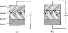
1401、1501 下部电极1401, 1501 lower electrode
1402、1502 缺氧型钽氧化物层1402, 1502 Oxygen-deficient tantalum oxide layer
1403、1503 上部电极1403, 1503 upper electrode
1404、1504 氧离子1404, 1504 Oxygen ions
3301 下部电极3301 lower electrode
3302 电阻变化层3302 resistance change layer
3303 上部电极3303 upper electrode
具体实施方式Detailed ways
下面参照附图对本发明的实施方式进行详细说明。Embodiments of the present invention will be described in detail below with reference to the accompanying drawings.
本发明的实施方式中的电阻变化型非易失性存储装置是将电阻变化元件和MOS晶体管串联连接而成的1T1R型非易失性存储装置,将电阻变化元件的电阻变化特性的模式固定的同时,按照固定的模式将MOS晶体管的结构最优化。The variable resistance nonvolatile memory device in the embodiment of the present invention is a 1T1R type nonvolatile memory device in which a variable resistance element and a MOS transistor are connected in series, and the mode of the variable resistance characteristic of the variable resistance element is fixed. At the same time, the structure of the MOS transistor is optimized according to a fixed pattern.
[本发明的基础数据][Basic data of the present invention]
作为准备,对与在本发明的电阻变化型非易失性存储装置中使用的2种电阻变化元件有关的基础数据进行说明。As a preparation, basic data related to two types of variable resistance elements used in the variable resistance nonvolatile memory device of the present invention will be described.
这些电阻变化元件是通过由不同材料形成的上下电极分别夹持由缺氧型钽氧化物形成的电阻变化层、以及由缺氧型铪氧化物形成的电阻变化层而构成的。These variable resistance elements are formed by sandwiching a variable resistance layer formed of an oxygen-deficient tantalum oxide and a variable resistance layer formed of an oxygen-deficient hafnium oxide between upper and lower electrodes formed of different materials.
这些电阻变化元件是以得到具有可逆的稳定的重写特性、并利用了电阻变化现象的非易失性存储元件为目的而由本申请发明人们发明的元件,分别在作为相关专利申请的日本特愿2007-267583号、以及日本特愿2008-121947号(专利文献)中进行了详细说明。These resistance change elements are elements invented by the inventors of the present application for the purpose of obtaining a nonvolatile memory element having reversible and stable rewriting characteristics and utilizing the resistance change phenomenon. Details are described in Japanese Patent Application No. 2007-267583 and Japanese Patent Application No. 2008-121947 (patent document).
本发明的电阻变化型非易失性存储装置中利用了如下特征,即,这些电阻变化元件所具有的、可将电阻变化特性固定为上述A模式及B模式中任意所希望的一种的特征。以下为了说明,引用上述相关专利申请的部分内容。The variable resistance nonvolatile memory device of the present invention utilizes the characteristic that the variable resistance characteristics of these variable resistance elements can be fixed to any desired one of the above-mentioned A mode and B mode. . In the following, for the sake of illustration, part of the content of the above-mentioned related patent application is cited.
另外,在本说明书中,“电阻变化元件”和“电阻变化型非易失性存储元件(或者简称为非易失性存储元件)”以相同的意思来使用。In addition, in this specification, "variable resistance element" and "variable resistance nonvolatile memory element (or simply referred to as nonvolatile memory element)" are used with the same meaning.
[在电阻变化层中使用了缺氧型钽氧化物的电阻变化元件][Resistance variable element using oxygen-deficient tantalum oxide in the resistance variable layer]
首先,对与使用了缺氧型钽氧化物的进行双极动作的电阻变化型非易失性存储元件有关的第一实验进行说明。First, a first experiment related to a bipolar-operating resistance variable nonvolatile memory element using an oxygen-deficient tantalum oxide will be described.
在第一实验中,通过将使用了缺氧型钽氧化物的进行双极动作的电阻变化型非易失性存储元件构成为仅在上下某一个电极附近容易发生电阻变化,由此来检验是否可得到可逆的稳定的重写特性。In the first experiment, it was examined whether the variable resistance nonvolatile memory element using an oxygen-deficient tantalum oxide and performing bipolar operation was easily changed only in the vicinity of one of the upper and lower electrodes. Reversible and stable rewriting characteristics can be obtained.
为了进行该检验,设想电阻变化的发生容易性根据电极的材料种类而变化,制作由不同材料的上下电极夹持缺氧型钽氧化物而成的结构的电阻变化元件,测定电阻变化特性。In order to perform this test, it was assumed that the ease of occurrence of resistance change varies depending on the type of electrode material, and a variable resistance element having a structure in which an oxygen-deficient tantalum oxide is sandwiched between upper and lower electrodes of different materials was fabricated, and the resistance change characteristic was measured.
下面对第一实验的结果进行说明。The results of the first experiment will be described below.
另外,在说明该检验结果之前,对缺氧型钽氧化物层的形成方法和氧含有率的适当的范围进行说明。In addition, before explaining the test results, the method of forming the oxygen-deficient tantalum oxide layer and the appropriate range of the oxygen content will be described.
然后,为了确认电阻变化的发生容易性是否依赖于电极材料,形成用由Pt、W、Ta、TaN(氮化钽)形成的电极夹持TaOx层而成的结构,说明对由电脉冲引起的电阻变化现象的情况进行调查而得到的结果。Then, in order to confirm whether the ease of occurrence of resistance change depends on the electrode material, a structure in which the TaOx layer is sandwiched between electrodes made of Pt, W, Ta, and TaN (tantalum nitride) was formed, and the response to electric pulses was explained. The results obtained by investigating the situation of the resistance change phenomenon.
并且最后,对用容易进行动作的电极材料和难以进行动作的电极材料夹持缺氧型钽氧化物而成的结构的电阻变化元件的电阻变化的测定结果进行说明。And finally, the measurement result of the resistance change of the variable resistance element having the structure in which the electrode material which is easy to operate and the electrode material which is difficult to operate is sandwiched between the oxygen-deficient tantalum oxide will be described.
[溅射时的氧流量比与钽氧化物层的氧含有率的关系][Relationship between the oxygen flow ratio during sputtering and the oxygen content of the tantalum oxide layer]
首先,对第一实验中的缺氧型钽氧化物层的制作条件以及氧含有率的解析结果进行说明。First, the production conditions of the oxygen-deficient tantalum oxide layer and the analysis results of the oxygen content in the first experiment will be described.
缺氧型钽氧化物层通过将Ta靶在氩(Ar)气体和O2(氧)气体气氛中进行溅射的所谓的反应性溅射法来制作。The oxygen-deficient tantalum oxide layer is produced by a so-called reactive sputtering method in which a Ta target is sputtered in an atmosphere of argon (Ar) gas and O2 (oxygen) gas.
第一实验中的具体的缺氧型钽氧化物的制作方法如下所述。The specific method for producing the oxygen-deficient tantalum oxide in the first experiment is as follows.
首先,将基板设置在溅射装置内,将溅射装置内抽真空至7×10⁻⁴Pa左右。以Ta为靶,将功率设为250W,将Ar气体和O2气体合并得到的总气体压力设为3.3Pa,将基板的设定温度设为30℃,进行溅射。这里,使O2气体相对于Ar气体的流量比从0.8%变化至6.7%。First, the substrate is placed in a sputtering apparatus, and the inside of the sputtering apparatus is evacuated to about 7×10⁻⁴ Pa. Using Ta as the target, the power was set to 250W, the total gas pressure obtained by combining Ar gas andO2 gas was set to 3.3Pa, and the set temperature of the substrate was set to 30°C to perform sputtering. Here, the flow rate ratio of Ogas to Ar gas was varied from 0.8% to 6.7%.
首先,由于目的在于调查组成,因此,作为基板,使用在硅(Si)上堆积了200nm的SiO2的基板,按钽氧化物层的膜厚为约100nm的方式调整溅射时间。First, since the purpose was to investigate the composition, a substrate in which 200 nm ofSiO2 was deposited on silicon (Si) was used as the substrate, and the sputtering time was adjusted so that the film thickness of the tantalum oxide layer was about 100 nm.
通过卢瑟福背散射法(RBS法)及俄歇电子光谱法(AES法)对这样制作的钽氧化物层的组成进行解析而得到的结果如图4所示。Fig. 4 shows the results of analyzing the composition of the tantalum oxide layer produced in this way by the Rutherford backscattering method (RBS method) and the Auger electron spectroscopy (AES method).
从该图可以看出,在使氧分压比从0.8%变化到6.7%的情况下,钽氧化物层中的氧含有率从约35at%(TaO0.66)变化到约70at%(TaO2.3)。It can be seen from this figure that when the oxygen partial pressure ratio is changed from 0.8% to 6.7%, the oxygen content rate in the tantalum oxide layer changes from about 35 at% (TaO0.66 ) to about 70 at% (TaO2.3 ) .
从以上结果可以看出,钽氧化物层中的氧含有率可通过氧流量比进行控制,可以形成与作为钽的化学计量的氧化物的Ta2O5(TaO2.5)的氧含有率71.4at%相比氧不足的缺氧型钽氧化物。From the above results, it can be seen that the oxygen content rate in the tantalum oxide layer can be controlled by the oxygen flow rate ratio, and can form an oxygen content rate 71.4 at that of Ta2 O5 (TaO2.5 ), which is a stoichiometric oxide of tantalum. % compared to oxygen-deficient tantalum oxides with insufficient oxygen.
另外,在第一实验中,在钽氧化物层的解析中使用了卢瑟福背散射法(RBS)以及俄歇电子光谱法(AES),但是,也可以使用荧光X线分析法(XPS)或电子探针显微分析法(EPMA)等的仪器分析方法。In addition, in the first experiment, Rutherford backscattering method (RBS) and Auger electron spectroscopy (AES) were used for the analysis of the tantalum oxide layer, but fluorescent X-ray analysis method (XPS) can also be used Or an instrumental analysis method such as electron probe microanalysis (EPMA).
[缺氧型钽氧化物层的组成和电阻变化特性][Composition and resistance change characteristics of an oxygen-deficient tantalum oxide layer]
对在如上所述制作的缺氧型钽氧化物中具有何种程度的氧含有率的缺氧型钽氧化物显示电阻变化进行了调查。这里,作为夹持缺氧型钽氧化物层的电极的材料所使用的材料,上下的电极均为Pt。It was investigated to what extent the oxygen-deficient tantalum oxide having an oxygen content in the oxygen-deficient tantalum oxide produced as described above exhibits a change in resistance. Here, as the material used for the electrodes sandwiching the oxygen-deficient tantalum oxide layer, both the upper and lower electrodes are Pt.
在上下的电极使用Pt的情况下,如上所述,作为双极型的电阻变化型的非易失性元件是不适当的。但是,如后所述,Pt是非常容易显示电阻变化的电极材料,对于判定具有某氧含有率的缺氧型钽氧化物是否显示电阻变化而言,是最合适的材料。When Pt is used for the upper and lower electrodes, as described above, it is not suitable as a bipolar variable resistance nonvolatile element. However, as will be described later, Pt is an electrode material that is very likely to show a change in resistance, and is the most suitable material for determining whether an oxygen-deficient tantalum oxide having a certain oxygen content shows a change in resistance.
从以上的理由考虑,形成图5所示的非易失性存储元件500。From the above reasons, the
即,在单晶硅基板501上通过热氧化法形成厚度为200nm的氧化物层502,通过溅射法在氧化物层502上形成作为下部电极503的厚度为100nm的Pt薄膜。That is, an
然后,以Ta作为靶,通过反应性溅射法形成缺氧型钽氧化物层504。在第一实验中研究的范围内,与上述的分析试样同样,使O2气体的流量比从0.8%变化至6.7%,制作非易失性存储元件。缺氧型钽氧化物层504的膜厚形成为30nm。Then, using Ta as a target, an oxygen-deficient
然后,在缺氧型钽氧化物层504上通过溅射法堆积作为上部电极505的厚度为150nm的Pt薄膜。Then, a Pt thin film with a thickness of 150 nm was deposited as the
最后,通过光刻工序和干蚀工序形成元件区域506。另外,元件区域506是直径为3μm的圆形图案。Finally, an
测定如上所述制作的非易失性存储元件的电阻变化现象。其结果是,在使用了从图4的α点(氧流量比约1.7%、氧含有率约45at%)到β点(氧流量比约5%、氧含有率约65at%)的钽氧化膜的非易失性存储元件的情况下,高电阻值为低电阻值的5倍以上,是良好的。The resistance change phenomenon of the nonvolatile memory element produced as described above was measured. As a result, the tantalum oxide film from the α point (oxygen flow ratio of about 1.7% and oxygen content rate of about 45at%) to the β point (oxygen flow ratio of about 5% and oxygen content rate of about 65at%) in Fig. 4 was used. In the case of a nonvolatile memory element, the high resistance value is five times or more than the low resistance value, which is good.
图6(a)、图6(b)分别是对使用了具有α点及β点的氧含有率的钽氧化物层的非易失性存储元件测定相对于脉冲施加次数的电阻变化特性而得到的结果。Fig. 6(a) and Fig. 6(b) are obtained by measuring the resistance change characteristics with respect to the number of pulse application for a nonvolatile memory element using a tantalum oxide layer having an oxygen content ratio of α point and β point, respectively. the result of.
根据图6(a)、图6(b),可以判断在使用了具有α点以及β点的氧含有率的钽氧化物层的元件的情况下,高电阻值均为低电阻值的5倍以上,是良好的。From Fig. 6(a) and Fig. 6(b), it can be judged that in the case of an element using a tantalum oxide layer having an oxygen content rate of α point and β point, the high resistance value is five times that of the low resistance value. The above is good.
因此,可以说氧含有率为45~65at%的组成范围、即将电阻变化层表示成TaOx时x的范围为0.8≤x≤1.9的范围是更合适的电阻变化层的范围(氧含有率=45at%与x=0.8相对应,氧含有率=65at%与x=1.9相对应)。Therefore, it can be said that the composition range in which the oxygen content is 45 to 65 at%, that is, the range in which x is 0.8≤x≤1.9 when the variable resistance layer is expressed asTaOx , is a more suitable range for the variable resistance layer (oxygen content = 45 at % corresponds to x = 0.8, oxygen content = 65 at % corresponds to x = 1.9).
[将W、Ta、TaN用于上下的电极材料的电阻变化元件的电阻变化特性][Resistance change characteristics of resistance change elements using W, Ta, TaN as upper and lower electrode materials]
然后,为了确认电阻变化的发生容易性是否依赖于电极材料,制作用由作为Pt以外的材料的W、Ta、TaN形成的下部电极503和上部电极505夹持缺氧型钽氧化物层504而成的结构,说明对由电脉冲引起的电阻变化的情况进行调查而得到的结果。Then, in order to confirm whether the ease of occurrence of resistance change depends on the electrode material, the
另外,这里以只评价电阻变化的发生容易性为目的而进行了实验,因此,将上下的电极材料设为相同。此外,将使用的缺氧型钽氧化物的氧含有率设为适当的氧含有率的范围的大致中间的58at%(TaO1.38)。元件的形成方法与上述大致相同,将Pt、W、Ta、TaN中的任意一种均通过溅射法进行堆积。In addition, since the experiment was performed here for the purpose of evaluating only the easiness of occurrence of resistance change, the upper and lower electrode materials were made the same. In addition, the oxygen content of the oxygen-deficient tantalum oxide used was set to 58 at% (TaO1.38 ), which is approximately in the middle of the appropriate oxygen content range. The method of forming the element is substantially the same as above, and any of Pt, W, Ta, and TaN is deposited by the sputtering method.
首先,为了比较,对下部电极503和上部电极505中的任一个均利用由Pt形成的薄膜形成的非易失性存储元件(以下,表示为元件B)的电阻变化特性进行说明。First, for comparison, resistance change characteristics of a nonvolatile memory element (hereinafter referred to as element B) in which both the
图7(a)、图7(b)是这样制作的元件B的由电脉冲引起的电阻变化的测定结果。Fig. 7(a) and Fig. 7(b) show the measurement results of the resistance change of the element B produced in this way due to the electric pulse.
图7(a)是在下部电极503和上部电极505之间以脉冲宽度100nsec、并且以下部电极503为基准向上部电极505交替施加具有+3.0V和-1.5V的电压的电脉冲时的电阻的测定结果。Fig. 7 (a) is between the
此时,通过施加+3.0V的电压的电脉冲,电阻值成为800~1000Ω左右,在施加-1.5V的电压的电脉冲时,变为150Ω左右。即,示出了如下变化:向上部电极505施加比下部电极503高的电压的电脉冲时进行高电阻化。At this time, by applying an electric pulse at a voltage of +3.0V, the resistance value becomes about 800 to 1000Ω, and when an electric pulse at a voltage of −1.5V is applied, the resistance value becomes about 150Ω. That is, a change is shown in which resistance is increased when an electric pulse having a voltage higher than that of the
此外,虽然省略了详细情况,但是从追加的实验可以得出如下推断的结果:此时的电阻变化在上部电极505的附近发生。In addition, although the details are omitted, it can be deduced from additional experiments that the resistance change at this time occurs in the vicinity of the
然后,使施加的电压的平衡变化,使负的电压增大的情况的结果为图7(b)。此时,相对于下部电极503向上部电极505施加-3.0V和+1.5V的电压的电脉冲。于是,在施加-3.0V的电脉冲时进行高电阻化,电阻值成为600~800Ω左右,在施加+1.5V的电脉冲时进行低电阻化,电阻值成为150Ω左右。即,在向上部电极505施加比下部电极503高的电压的电脉冲时进行低电阻化,与测定图7(a)时显示完全相反的动作。Then, the result of changing the balance of the applied voltage and increasing the negative voltage is shown in FIG. 7( b ). At this time, electric pulses at voltages of −3.0 V and +1.5 V are applied to the
此外,虽然省略了详细情况,但是,从追加的实验可以得出如下的推断的结果:此时的电阻变化在下部电极503的附近发生。In addition, although the details are omitted, it can be deduced from additional experiments that the resistance change at this time occurs in the vicinity of the
然后,对下部电极503和上部电极505中的任一个均用由W形成的薄膜形成的非易失性存储元件(以下,表示为元件C)的电阻变化特性进行说明。Next, resistance change characteristics of a nonvolatile memory element (hereinafter referred to as element C) in which either the
图8(a)、图8(b)是这样制作的元件C的由电脉冲引起的电阻变化的测定结果。Fig. 8(a) and Fig. 8(b) show the measurement results of the resistance change of the element C produced in this way due to the electric pulse.
图8(a)表示以在上部电极505的附近发生电阻变化(上部电极模式)为目的、以下部电极503为基准向上部电极505交替施加+7V和-5V时的电阻值的变化。上部电极模式为通过以下部电极为基准向上部电极施加正电压而发生高电阻化的模式,与上述的B模式对应。8( a ) shows changes in resistance value when +7V and -5V are alternately applied to the
从图8(a)可知,在脉冲数到30次左右为止时,虽然弱,但是可观测到在B模式下的电阻变化,在施加+7V的电脉冲时进行高电阻化,在施加-5V的电脉冲时进行低电阻化。但是,如果脉冲数超过30次,则几乎无法观测到电阻变化。From Figure 8(a), it can be seen that when the number of pulses reaches about 30 times, although the resistance change in the B mode can be observed weakly, when the electric pulse of +7V is applied, the resistance becomes high, and when -5V is applied Low resistance during electric pulse. However, when the number of pulses exceeds 30, almost no change in resistance can be observed.
相反,图8(b)表示以使在下部电极503的附近发生电阻变化(下部电极模式)为目的、向上部电极505交替施加+5V和-7V时的电阻值的变化。下部电极模式为通过以上部电极为基准向下部电极施加正电压而发生高电阻化的模式,与上述的A模式相对应。In contrast, FIG. 8( b ) shows the change in resistance value when +5V and -7V are alternately applied to the
从图8(b)可知,此时几乎无法观测到电阻值的变化,电阻值在30Ω左右成为稳定的值。As can be seen from FIG. 8( b ), at this time, almost no change in the resistance value can be observed, and the resistance value becomes a stable value at about 30Ω.
这里,如果对图7(a)的将上下的电极由Pt形成的元件B的结果与图8(a)的结果进行比较,则可知在将W用作电极时,明显变得难以发生电阻变化。Here, comparing the results of the element B in which the upper and lower electrodes are formed of Pt in FIG. .
在作为元件B的测定结果的图7(a)中,低电阻状态的电阻值为150Ω,高电阻状态的电阻值为约1000Ω、以比率计发生了7倍左右的变化,相对于此,在作为将W用作电极材料的元件C的测定结果的图8(a)中,即使在进行大的电阻变化的范围中,最高也仅在50Ω与100Ω之间发生电阻变化,作为比率,只是2倍左右的变化。In Fig. 7(a) which is the measurement result of element B, the resistance value in the low-resistance state is 150Ω, and the resistance value in the high-resistance state is about 1000Ω, which is a change of about 7 times in ratio. In FIG. 8( a ), which is the measurement result of an element C using W as an electrode material, even in the range where a large resistance change occurs, the resistance change occurs only between 50Ω and 100Ω at the highest, and the ratio is only 2. times change.
对于施加的电压,在图7(a)的测定时,为+3.0V和-1.5V,相对于此,在图8(a)中,尽管施加了+7V和-5V的非常高的电压,也几乎无法看到电阻变化。The applied voltage was +3.0V and -1.5V at the time of measurement in FIG. 7(a), but in FIG. Also almost no resistance change can be seen.
如上所示,可知在将W用作电极时,与将Pt用作电极的情况相比,明显难以发生电阻变化。As described above, it can be seen that when W is used as an electrode, resistance change is significantly less likely to occur than when Pt is used as an electrode.
以上的结果表示,将缺氧型钽氧化物用于电阻变化层的电阻变化元件的动作对使用的电极的材料有非常强的依赖性。即,至少可明确在将Pt用作电极的情况下容易发生电阻变化,在将W用作电极的情况下,难以发生电阻变化。The above results show that the operation of the variable resistance element using the oxygen-deficient tantalum oxide as the variable resistance layer is very strongly dependent on the material of the electrodes used. That is, at least it is clear that when Pt is used as an electrode, resistance change easily occurs, and when W is used as an electrode, resistance change hardly occurs.
此外,虽然未作详细说明,但是,也制作了将Ta或TaN用作上下的电极的电阻变化元件,并进行了电阻变化特性的测定。In addition, although not described in detail, variable resistance elements using Ta or TaN as upper and lower electrodes were also manufactured, and resistance variable characteristics were measured.
图9(a)、图9(b)是下部电极503和上部电极505中的任一个均使用了Ta的元件D的电阻变化特性。FIGS. 9( a ) and 9 ( b ) show resistance change characteristics of an element D in which Ta is used for both the
图9(a)是在向上部电极505施加+7V和-5V的电脉冲的情况下的测定结果,图9(b)是在向上部电极505施加+5V和-7V的电脉冲的情况下的测定结果。在哪一种情况下,几乎均未发生电阻变化。Fig. 9(a) is the measurement result when electric pulses of +7V and -5V are applied to the
此外,图10(a)是下部电极503和上部电极505中的任一个均使用了TaN的元件E的电阻变化特性。图10(a)是在向上部电极505施加+7V和-5V的电脉冲的情况下的测定结果,图10(b)是在向上部电极505施加+5V和-7V的电脉冲的情况下的测定结果。在该情况下,仅发生了可以说几乎没有变化的程度的电阻变化。In addition, FIG. 10( a ) shows resistance change characteristics of an element E in which TaN is used for both the
如上所述,除了W以外,也存在难以发生电阻变化的材料。As described above, there are materials other than W that are less prone to change in resistance.
[将W和Pt用作电极的电阻变化元件的电阻变化特性][Resistance change characteristics of a resistance change element using W and Pt as electrodes]
然后,说明由作为容易发生电阻变化的材料的Pt、和作为难以发生电阻变化的材料且工艺稳定性高的材料的W夹持缺氧型钽氧化物的形式的电阻变化元件即元件F的电阻变化特性。Next, the resistance of element F which is a variable resistance element in the form of an oxygen-deficient tantalum oxide sandwiched between Pt, a material that easily changes resistance, and W, a material that is difficult to change resistance and has high process stability, will be described. change characteristics.
准备的元件是使用W薄膜作为下部电极503、使用Pt薄膜作为上部电极505而制作的。W薄膜とPt薄膜分别是通过将W靶和Pt靶在Ar气体中进行溅射而堆积成的。The prepared element was fabricated using a W thin film as the
如上所述制作的元件F的由电脉冲引起的电阻变化的情况如图11(a)、图11(b)所示。The state of the resistance change by the electric pulse of the element F fabricated as above is shown in FIG. 11( a ) and FIG. 11( b ).
图11(a)表示以使在上部电极505的附近的电阻变化发生(B模式)为目的、以下部电极503为基准向上部电极505交替施加+2.5V和-1.5V时的电阻值的变化。此时,电阻值在施加了+2.5V的电脉冲时成为约600Ω,在施加了-1.5V的电脉冲时成为60Ω地稳定变化。FIG. 11( a ) shows the change in resistance value when +2.5V and -1.5V are alternately applied to the
另一方面,以使在下部电极503的附近的电阻变化发生(A模式)为目的、以下部电极503为基准向上部电极505交替施加+1.5V和-2.5V时的电阻值的变化如图11(b)所示。此时,电阻变化仅在60Ω与100Ω之间发生电阻变化,与为了使B模式的电阻变化发生的电压施加相比,仅发生可无视的程度的电阻变化。On the other hand, the change in resistance value when +1.5V and -2.5V are alternately applied to the
从以上的图11(a)、图11(b)的结果来看,元件F显示了仅在单侧的电极附近发生电阻变化的进行双极动作的电阻变化型的非易失性存储元件的理想的动作。From the above results of FIG. 11(a) and FIG. 11(b), element F shows the performance of a variable resistance nonvolatile memory element that performs bipolar operation in which resistance changes only in the vicinity of one electrode. Ideal for action.
此外,也未发现A模式和B模式混杂的现象。In addition, no mixing of A-mode and B-mode was found.
例如,图12表示向与得到图11(a)、图11(b)的测定结果的元件F不同的元件(同一基板上的不同元件)施加1000次左右的电脉冲的结果,但是,可以看到电阻变化现象非常稳定地发生。For example, Fig. 12 shows the result of applying electric pulses about 1000 times to an element (a different element on the same substrate) different from the element F that obtained the measurement results of Fig. 11(a) and Fig. 11(b), but it can be seen that until the resistance change phenomenon occurs very stably.
从以上情况可知,由于通过形成用容易发生电阻变化现象的电极、和难以发生电阻变化现象的电极夹持电阻变化层而成的结构,能使在所希望的单侧的电极侧进行电阻变化,因此可制作稳定动作的、显示出优选的双极动作的电阻变化型的非易失性存储元件。From the above, it can be seen that by forming a structure in which the variable resistance layer is sandwiched between electrodes that are prone to resistance change phenomenon and electrodes that are difficult to cause resistance change phenomenon, the resistance change can be performed on the desired side of the electrode, Therefore, a variable resistance nonvolatile memory element that operates stably and exhibits preferable bipolar operation can be fabricated.
此外,施加电压与电阻值的关系显示出如下动作:在向容易发生电阻变化的电极施加正的电压的电脉冲时,电阻值增高,在施加负的电压的电脉冲时,电阻值降低。In addition, the relationship between the applied voltage and the resistance value shows that when a positive voltage electric pulse is applied to an electrode prone to resistance change, the resistance value increases, and when a negative voltage electric pulse is applied, the resistance value decreases.
[与上下的电极材料种类对应的电阻变化元件的电阻变化特性][Resistance change characteristics of resistance change elements corresponding to types of upper and lower electrode materials]
然后,示出第二实验的结果,该第二实验对电极材料不同的几种元件评价了电阻变化的发生容易性。Next, the results of a second experiment evaluating the easiness of occurrence of resistance change with respect to several elements having different electrode materials are shown.
作为第二实验的结果将下部电极503固定为W、将上部电极505用Pt以外的不同的材料构成的多种元件的电阻变化的情况进行说明。这里,将下部电极503固定为W是因为W是比较稳定的材料、且加工也比较容易。As a result of the second experiment, a case where the resistance of various elements in which the
另外,元件的制作方法与第一实验中说明的方法相同,下部电极503、上部电极505都通过溅射法形成。此外,作为电阻变化材料的缺氧型钽氧化物也是将钽金属在O2和Ar中进行溅射而制作的。In addition, the fabrication method of the device was the same as that described in the first experiment, and the
为了调查与电极的不同相对应的电阻变化的特性,缺氧型钽氧化物的组成设定为完全相同。即,在将氧含有率固定为约58at%的缺氧型钽氧化物(表示为TaOx时,x为1.38)。In order to investigate the characteristics of the resistance change corresponding to the difference in electrodes, the compositions of the oxygen-deficient tantalum oxides were set to be completely the same. That is, an oxygen-deficient tantalum oxide (when expressed as TaOx , x is 1.38) with the oxygen content constant at about 58 at %.
此外,在第二实验中,由于将下部电极503设为难以动作的W,因此,将电阻值的变化几乎不产生的A模式(在相对于上部电极向下部电极施加高电压时进行高电阻化的模式)的结果省略,仅示出B模式(在相对于下部电极向上部电极施加高电压时进行高电阻化的模式)的结果。在B模式中进行电阻变化时的电脉冲的电压根据元件而存在若干不同,但是,将下部电极设为电压的基准,将进行高电阻化时的电压设为+1.8~+2.0V,将进行低电阻化时的电压设为-1.3~-1.6V。In addition, in the second experiment, since the
在图13(a)~图13(h)中总结了测定结果。The measurement results are summarized in Fig. 13(a) to Fig. 13(h).
首先,在看了图13(a)的作为上部电极使用Ir的元件G、图13(b)的作为上部电极使用Ag(银)的元件H、图13(c)的作为上部电极使用Cu(铜)的元件I的结果后,可知较稳定地以大的幅度发生了电阻变化。然后,在图13(d)的作为上部电极使用Ni(镍)的元件J、图13(h)的作为上部电极使用TaN的元件N中,虽然可看见若干的电阻变化,但是其变化幅度小。First, after looking at the element G using Ir as the upper electrode in FIG. 13(a), the element H using Ag (silver) as the upper electrode in FIG. From the results of the element I of copper), it can be seen that the resistance change occurred relatively stably with a large range. Then, in the element J using Ni (nickel) as the upper electrode in FIG. 13(d) and the element N using TaN as the upper electrode in FIG. .
然后,在图13(e)的作为上部电极使用Ta的元件K、图13(f)的作为上部电极使用Ti(钛)的元件L、图13(g)的作为上部电极使用Al(铝)的元件M中,完全没有观测到电阻变化现象。可以认为这些材料本质上具有难以产生电阻变化的性质。Then, the element K using Ta as the upper electrode in FIG. 13(e), the element L using Ti (titanium) as the upper electrode in FIG. 13(f), and the element L using Al (aluminum) as the upper electrode in FIG. In the element M, no resistance change phenomenon was observed at all. It is considered that these materials essentially have the property that resistance change is difficult to occur.
从以上的结果可知,在使用了缺氧型钽氧化物的非易失性存储元件中,存在容易产生电阻变化现象(容易进行动作)的材料、和难以产生电阻变化现象(难以进行动作)的材料。以第二实验的范围来说,容易进行动作的电极为Pt、Ir、Ag、Cu,难以进行动作的电极材料为W、Ni、Ta、Ti、Al、TaN。From the above results, it can be seen that in nonvolatile memory elements using oxygen-deficient tantalum oxide, there are materials that are prone to change in resistance (easy to operate) and materials that are difficult to change in resistance (difficult to operate). Material. In the scope of the second experiment, the electrodes that are easy to operate are Pt, Ir, Ag, and Cu, and the electrode materials that are difficult to operate are W, Ni, Ta, Ti, Al, and TaN.
如果形成通过这些材料的组合来夹持缺氧型钽氧化物的结构的电阻变化元件,则可得到没有模式混杂的稳定的电阻变化。其中,参照图7(a)、图11(b)、图13(d)、图13(h),在W、Ni、TaN电极的情况下,虽然微弱,但是还是可以观察到电阻变化。因此,在使用这些材料作为一个电极、使用例如在第二实验中完全观测不到电阻变化的电极材料即Ta、Ti、Al作为另一个电极的情况下,虽然微弱,但是可期待得到稳定的电阻变化。By forming a resistance variable element having a structure in which an oxygen-deficient tantalum oxide is sandwiched by a combination of these materials, a stable resistance change without mode mixing can be obtained. Among them, referring to FIG. 7(a), FIG. 11(b), FIG. 13(d), and FIG. 13(h), in the case of W, Ni, and TaN electrodes, resistance changes can be observed although weak. Therefore, when these materials are used as one electrode and Ta, Ti, and Al, electrode materials whose resistance change is not observed at all in the second experiment, for example, are used as the other electrode, a weak but stable resistance can be expected. Variety.
然后,对电阻变化本身发生的机理和电阻变化的发生容易性的材料依赖性进行了若干考察。Then, several considerations were made on the mechanism by which the resistance change itself occurs and the material dependence of the ease with which the resistance change occurs.
图14是对第一实验和第二实验的结果进行总结而得到的图。在横轴描绘电极材料,在纵轴描绘标准电极电位。图14的○表示电阻变化容易发生,△表示变化的比例小但是发生了电阻变化,×表示未发生电阻变化。另外,TiN(氮化钛)是未在第一实验及第二实验中使用的电极材料,用于参考而用·示出。FIG. 14 is a graph summarizing the results of the first experiment and the second experiment. The electrode material is plotted on the horizontal axis, and the standard electrode potential is plotted on the vertical axis. ○ in FIG. 14 indicates that resistance change occurs easily, △ indicates that resistance change occurs at a small rate of change, and × indicates that resistance change does not occur. In addition, TiN (titanium nitride) is an electrode material which was not used in the first experiment and the second experiment, and is indicated by · for reference.
在图14中,TaN、TiN以外的电极材料的标准电极电位为非专利文献1:“CRC HANDBOOK of CHEMISTRY and PHYSICS(化学及物理CRC手册),DAVID R.LIDE Editor-in-chif,84th Edition 2003-2004,CRC PRESS”中公开的文献值,TaN、TiN的标准电极电位是发明人们测定的数据。In Figure 14, the standard electrode potentials of electrode materials other than TaN and TiN are non-patent literature 1: "CRC HANDBOOK of CHEMISTRY and PHYSICS (Chemical and Physical CRC Handbook), DAVID R.LIDE Editor-in-chif, 84th Edition 2003 -2004, CRC PRESS", the standard electrode potentials of TaN and TiN are the data measured by the inventors.
发明人们通过用Solartron公司制的电化学测定系统SI1280B构成的3电极系的恒电位仪对含有TaN、TiN的几种电极材料的标准电极电位进行测定。作为测定条件,使用成为测定对象的电极材料作为作用极,使用Pt电极作为对极,使用Ag/AgCl电极作为参照极,作为电解液,将7ml的1wt%KCl在N2鼓泡的情况下来使用。The inventors measured the standard electrode potentials of several electrode materials including TaN and TiN using a three-electrode system potentiostat consisting of an electrochemical measurement system SI1280B manufactured by Solartron Corporation. As the measurement conditions, the electrode material to be measured is used as the working electrode, the Pt electrode is used as the counter electrode, the Ag/AgCl electrode is used as the reference electrode, and 7ml of 1wt% KCl is bubbled inN2 as the electrolyte solution. .
通过在这样的条件下探索作用极与对极之间的电位平衡点,对电极材料相对于Ag/AgCl电极的电位平衡点下的电位进行测定之后,将在测定的电位中加上+0.196V而得到的值作为电极材料相对于标准氢电极的电位(即标准电极电位)。By exploring the potential balance point between the working electrode and the counter electrode under such conditions, after measuring the potential at the potential balance point of the electrode material relative to the Ag/AgCl electrode, add +0.196V to the measured potential The obtained value was taken as the potential of the electrode material relative to the standard hydrogen electrode (ie, the standard electrode potential).
观察图14可知,在标准电极电位比作为电阻变化层的构成元素的Ta高的材料的情况下,发生了电阻变化,在标准电极电位比Ta低的材料的情况下,变得难以发生电阻变化。并且,可知标准电极电位的差越大,越容易发生电阻变化,随着标准电极电位的差减小,变得难以发生电阻变化。As can be seen from FIG. 14 , in the case of a material having a standard electrode potential higher than Ta, which is a constituent element of the variable resistance layer, a resistance change occurs, and in the case of a material having a standard electrode potential lower than Ta, a resistance change becomes less likely to occur. . In addition, it can be seen that the larger the difference in standard electrode potential, the easier the resistance change will be, and the smaller the difference in standard electrode potential, the less likely the resistance change will be.
一般情况下,标准电极电位是氧化的容易性的一个指标,意味着该值越大,越难以氧化,越小越容易氧化。从该情况可以推测,氧化的容易性对电阻变化现象的机理起很大的作用。In general, the standard electrode potential is an indicator of the ease of oxidation, meaning that the larger the value, the more difficult it is to oxidize, and the smaller it is, the easier it is to oxidize. From this fact, it is presumed that the ease of oxidation plays a large role in the mechanism of the resistance change phenomenon.
基于以上结果,考虑电阻变化的机理。首先,使用图15(a)、图15(b)对通过电阻变化容易发生的材料(标准电极电位大、难以氧化的材料)构成上部电极的情况进行说明。Based on the above results, the mechanism of the resistance change was considered. First, a case where the upper electrode is formed of a material (a material with a high standard electrode potential and difficult to oxidize) that easily changes in resistance will be described with reference to FIGS. 15( a ) and 15 ( b ).
如图15(a)所示,对于由下部电极1401、缺氧型钽氧化物层1402、用比Ta难氧化的材料构成的上部电极1403构成的电阻变化元件,在相对于下部电极1401向上部电极1403施加高电压时,缺氧型钽氧化物中的氧原子成为离子,通过电场进行移动,并集中到上部电极1403的界面附近。As shown in FIG. 15(a), for a variable resistance element composed of a
但是,构成上部电极1403的金属与Ta相比难以氧化,因此,氧离子1404成为滞留在缺氧型钽氧化物层1402与上部电极1403的界面的状态,并在界面附近与Ta结合,形成氧浓度高的缺氧型钽氧化物。通过该情况,元件进行高电阻化。However, since the metal constituting the
然后,如图15(b)所示,在向下部电极1401施加高的电压时,氧原子再次成为氧离子,返回到缺氧型钽氧化物层1402的内部。由此,可以想到发生了低电阻化。Then, as shown in FIG. 15( b ), when a high voltage is applied to the
然后,对通过比Ta容易氧化的材料构成上部电极的情况进行了说明的图为图16(a)、图16(b)。Next, Fig. 16(a) and Fig. 16(b) explain the case where the upper electrode is formed of a material that is easier to oxidize than Ta.
如图16(a)所示,对于由下部电极1501、缺氧型钽氧化物层1502、用比Ta容易氧化的材料形成的上部电极1503构成的电阻变化元件,相对于下部电极1501向上部电极1503施加高的电压时,缺氧型钽氧化物中的氧原子成为离子,通过电场移动,集中到上部电极1503的界面附近。As shown in FIG. 16(a), for a variable resistance element composed of a
此时,由于上部电极1503比Ta容易氧化,因此,氧离子1504被吸入到上部电极1503的内部,与形成上部电极1503的材料发生结合。此时,与图15(a)不同,在缺氧型钽氧化物层1502与上部电极1503的界面未形成高电阻层,而且,相对于构成上部电极1503的元素的数量,氧离子的数量少,因此,电阻值几乎不上升。At this time, since the
相反,如图16(b)所示,在向下部电极1501施加高的电压的情况下,吸入到上部电极1503的氧与上部电极件的结合更加稳定,因此,可以认为难以返回到缺氧型钽氧化物层1502中,电阻值不进行较大地变化。On the contrary, as shown in FIG. 16(b), when a high voltage is applied to the
如果在图15(a)、图15(b)、图16(a)、及图16(b)中,在构成上部电极的材料的氧化的容易性与Ta相同程度的情况下,认为产生上述的两个例子的中间的变化,发生微弱的电阻变化。If in Fig. 15(a), Fig. 15(b), Fig. 16(a), and Fig. 16(b), the ease of oxidation of the material constituting the upper electrode is at the same level as Ta, it is considered that the above-mentioned In the middle of the two examples, a weak resistance change occurs.
从以上结果可知,在将缺氧型钽氧化物用于电阻变化层的非易失性存储元件的情况下,在上部电极与下部电极中使用具有不同的标准电极电位的材料即可。From the above results, it can be seen that when an oxygen-deficient tantalum oxide is used for a nonvolatile memory element of a variable resistance layer, materials having different standard electrode potentials may be used for the upper electrode and the lower electrode.
由此,在单侧的电极附近优势地发生电阻变化,能实现理想的双极型的电阻变化。而且,不会发生电阻变化模式的混杂,使得稳定的电阻变化动作变得可能。As a result, resistance change occurs predominantly in the vicinity of one electrode, and an ideal bipolar resistance change can be realized. Furthermore, no confusion of resistance change modes occurs, enabling stable resistance change operation.
更优选的是,对于一个电极材料,使用比Ta的标准电极电位大、且差较大的材料,对于另一个电极材料,使用比Ta的标准电极电位大、且差较小的材料即可。More preferably, for one electrode material, a material having a standard electrode potential larger than Ta and having a larger difference is used, and for the other electrode material, a material having a standard electrode potential larger than Ta and having a smaller difference may be used.
进一步优选的是,对于一个电极材料,使用比Ta的标准电极电位大的材料,对于另一个电极材料,使用比Ta的标准电极电位小的材料即可。It is more preferable to use a material having a standard electrode potential higher than Ta for one electrode material, and use a material having a standard electrode potential lower than Ta for the other electrode material.
另外,作为第二实验的结果,虽然没有记述,但是,对于分别使用TaN及Pt作为下部电极及上部电极的电阻变化元件,可得到显示出发生了稳定的电阻变化现象的良好的实验结果。In addition, as the results of the second experiment, although not described, good experimental results showing stable resistance change phenomenon were obtained for the variable resistance element using TaN and Pt as the lower electrode and the upper electrode, respectively.
TaN的标准电极电位根据发明人们的测定为+0.48eV,Pt及Ta的标准电极电位根据非专利文献1分别为+1.18eV、-0.6eV。The standard electrode potential of TaN is +0.48eV according to the measurement of the inventors, and the standard electrode potentials of Pt and Ta are respectively +1.18eV and -0.6eV according to
该例为使用比Ta的标准电极电位大且差较大的材料即Pt作为上部电极、使用比Ta的标准电极电位大且差较小的材料即TaN作为下部电极的一例。This example is an example of using Pt, which is a material with a standard electrode potential larger and a larger difference than Ta, as the upper electrode, and TaN, which is a material with a standard electrode potential larger than Ta and a smaller difference, as the lower electrode.
即,可以认为在该例中,通过使用满足与上述的标准电极电位有关的条件的TaN及Pt作为电极材料,可得到作为第二实验的结果说明的作用效果。That is, it is considered that in this example, by using TaN and Pt satisfying the above-mentioned conditions related to the standard electrode potential as electrode materials, the effect explained as the result of the second experiment can be obtained.
此外,作为其他例子,可以分别使用TiN及Pt作为下部电极及上部电极。TiN的标准电极电位根据发明人们的上述测定为+0.55eV。因此,TiN与Pt的组合由于满足与在电阻变化层中使用钽氧化物的情况的标准电极电位有关的条件,因此,通过使用TiN及Pt作为电极材料,可以期待作为第二实验的结果所说明的作用效果。In addition, as another example, TiN and Pt may be used as the lower electrode and the upper electrode, respectively. The standard electrode potential of TiN is +0.55 eV based on the above-mentioned measurement by the inventors. Therefore, since the combination of TiN and Pt satisfies the conditions related to the standard electrode potential in the case of using tantalum oxide in the variable resistance layer, by using TiN and Pt as electrode materials, it can be expected that effect.
而且,作为其他例子,也可以使用Au(金)或Pd作为电极材料。根据非专利文献1,Au、Pd的标准电极电位分别为+1.692eV、+0.951eV,比Ta的标准电极电位-0.6eV高。因此,在使用钽氧化物作为电阻变化层时,作为容易进行电阻变化的电极材料,使用Au及Pd中的一种,且作为难以进行电阻变化的电极材料,使用标准电极电位比Au及Pd中的上述一种低的材料(例如,标准电极电位为+0.1eV的W),由此可期待作为第二实验的结果所说的作用效果。Furthermore, as another example, Au (gold) or Pd may be used as an electrode material. According to
此外,从上述机理可以看出,表现出在向容易发生电阻变化的电极施加正的电压的电脉冲时,电阻值增高,在施加负的电压的电脉冲时,电阻值降低的动作。In addition, from the above mechanism, it can be seen that when a positive voltage electric pulse is applied to an electrode prone to resistance change, the resistance value increases, and when a negative voltage electric pulse is applied, the resistance value decreases.
[使用缺氧型铪氧化物作为电阻变化层的电阻变化元件][Resistance variable element using oxygen-deficient hafnium oxide as resistance variable layer]
然后,作为其他相同的例子,对与将缺氧型铪氧化物作为电阻变化层使用的进行双极动作的非易失性存储元件有关的第3实验进行说明。Next, as another similar example, a third experiment related to a bipolar nonvolatile memory element using an oxygen-deficient hafnium oxide as a variable resistance layer will be described.
与第一实验的说明相同,首先,说明缺氧型铪氧化物层的形成方法、和氧含有率的适当的范围。Similar to the description of the first experiment, first, the formation method of the oxygen-deficient hafnium oxide layer and the appropriate range of the oxygen content will be described.
然后,为了确认电阻变化的发生容易性是否依赖于电极材料,形成用由Al、Ti、Ta、W、Cu、Pt形成的电极夹持HfOx层的结构,并说明了对由电脉冲引起的电阻变化现象的情况进行调查而得到的结果。并且,最后,对用容易进行动作的电极材料和难以进行动作的电极材料夹持缺氧型铪氧化物而成的结构的电阻变化元件的电阻变化的测定结果进行说明。Then, in order to confirm whether the ease of occurrence of resistance change depends on the electrode material, a structure in which theHfOx layer is sandwiched between electrodes made of Al, Ti, Ta, W, Cu, and Pt was formed, and the response to the electric pulse induced The results obtained by investigating the situation of the resistance change phenomenon. And finally, the measurement results of the resistance change of the resistance variable element having the structure in which the oxygen-deficient hafnium oxide is sandwiched between the electrode material which is easy to operate and the electrode material which is difficult to operate will be described.
[溅射时的氧流量比与铪氧化物层的氧含有率的关系][Relationship between the oxygen flow ratio during sputtering and the oxygen content of the hafnium oxide layer]
首先,对第3实验中的缺氧型铪氧化物层的制作条件及氧含有率的解析结果进行说明。First, the production conditions of the oxygen-deficient hafnium oxide layer and the analysis results of the oxygen content in the third experiment will be described.
缺氧型铪氧化物层是通过将Hf(铪)靶在Ar气体和O2气体气氛中进行溅射的所谓的反应性溅射法而制得的。第3实验中的具体的缺氧型铪氧化物的制作方法如下所述。The oxygen-deficient hafnium oxide layer is produced by a so-called reactive sputtering method in which an Hf (hafnium) target is sputtered in an atmosphere of Ar gas and O2 gas. The specific method of producing the oxygen-deficient hafnium oxide in the third experiment is as follows.
首先,在溅射装置内设置基板,将溅射装置内抽真空至3×10⁻⁵Pa左右。将Hf作为靶,将功率设为300W,将由Ar气体和O2气体合并而得的总气体压力设为0.9Pa,将基板的设定温度设为30℃,进行溅射。这里,使O2气体相对于Ar气体的流量比从2%变化至4.2%。First, a substrate is set in a sputtering apparatus, and the inside of the sputtering apparatus is evacuated to about 3×10⁻⁵ Pa. Sputtering was performed using Hf as a target, the power at 300W, the total gas pressure obtained by combining Ar gas andO2 gas at 0.9Pa, and the set temperature of the substrate at 30°C. Here, the flow rate ratio of Ogas to Ar gas was varied from 2% to 4.2%.
首先,由于以调查组成为目的,因此,作为基板,使用在Si上堆积200nm的SiO2而成的基板,以铪氧化物层的膜厚为约50nm的方式调整溅射时间。First, for the purpose of investigating the composition, a substrate obtained by depositing 200 nm of SiO2 on Si was used as the substrate, and the sputtering time was adjusted so that the film thickness of the hafnium oxide layer was about 50 nm.
对这样制作的铪氧化物层的组成通过卢瑟福背散射法(RBS法)进行解析而得的结果如图17所示。FIG. 17 shows the results of analyzing the composition of the hafnium oxide layer produced in this way by the Rutherford backscattering method (RBS method).
从该图可知,在使氧流量比从2%变化至4.2%时,铪氧化物层中的氧含有率从约37.7at%(HfO0.6)变化至约69.4at%(HfO2.3)。It can be seen from the figure that when the oxygen flow ratio is changed from 2% to 4.2%, the oxygen content in the hafnium oxide layer changes from about 37.7 at% (HfO0.6 ) to about 69.4 at% (HfO2.3 ).
从以上结果可知:通过氧流量比可控制铪氧化物层中的氧含有率;形成了从与Hf的化学计量的氧化物即HfO2的氧含有率66.7at%相比氧不足的缺氧型铪氧化物到被认为氧过量地含有的铪氧化物。From the above results, it can be seen that the oxygen content rate in the hafnium oxide layer can be controlled by the oxygen flow ratio; an oxygen-deficient type is formed from the oxygen content rate 66.7 at% ofHfO2 , which is the stoichiometric oxide of Hf. Hafnium oxide to hafnium oxide considered to contain oxygen in excess.
另外,在第3实验中,在铪氧化物层的解析中利用了卢瑟福背散射法(RBS),但是也可以利用俄歇电子光谱法(AES)、荧光X线分析法(XPS)、电子探针显微分析法(EPMA)等仪器分析方法。In addition, in the third experiment, Rutherford backscattering method (RBS) was used for the analysis of the hafnium oxide layer, but Auger electron spectroscopy (AES), fluorescent X-ray analysis method (XPS), Electron probe microanalysis (EPMA) and other instrumental analysis methods.
[缺氧型铪氧化物层的电阻变化特性][Resistance change characteristics of oxygen-deficient hafnium oxide layer]
对如上所述制作的缺氧型铪氧化物中具有何种程度的氧含有率的缺氧型铪氧化物显示出电阻变化进行了调查。这里,作为夹持缺氧型铪氧化物层的电极的材料使用的材料,上下的电极均为Pt。It was investigated to what extent the oxygen-deficient hafnium oxide having an oxygen content in the oxygen-deficient hafnium oxide produced as described above exhibits a change in electrical resistance. Here, as a material used as a material for the electrodes sandwiching the oxygen-deficient hafnium oxide layer, both the upper and lower electrodes are Pt.
在上下的电极使用Pt的情况下,如上所述,作为双极型的电阻变化型的非易失性元件是不适当的。但是,如后所述,Pt是非常容易显示电阻变化的电极材料,对于判定具有某氧含有率的缺氧型铪氧化物是否显示电阻变化而言,是最合适的材料。When Pt is used for the upper and lower electrodes, as described above, it is not suitable as a bipolar variable resistance nonvolatile element. However, as will be described later, Pt is an electrode material that is very likely to show a change in resistance, and is the most suitable material for determining whether an oxygen-deficient hafnium oxide having a certain oxygen content shows a change in resistance.
从以上的理由考虑,形成图5的非易失性存储元件。From the above reasons, the nonvolatile memory element of FIG. 5 is formed.
即,在单晶硅基板501上通过热氧化法形成厚度为200nm的氧化物层502,通过溅射法在氧化物层502上形成作为下部电极503的厚度为100nm的Pt薄膜。That is, an
然后,以Hf作为靶,通过反应性溅射法形成缺氧型铪氧化物层504。在第3实验中研究的范围内,与上述的分析试样同样,使O2气体的流量比从2%变化至4.2%,制作非易失性存储元件。缺氧型铪氧化物层504的膜厚形成为30nm。Then, using Hf as a target, an oxygen-deficient
然后,在缺氧型铪氧化物层504上通过溅射法堆积作为上部电极505的厚度为150nm的Pt薄膜。Then, a Pt thin film with a thickness of 150 nm was deposited as the
最后,通过光刻工序和干蚀工序形成元件区域506。另外,元件区域506是直径为3μm的圆形图案。Finally, an
测定如上所述制作的非易失性存储元件的电阻变化现象。其结果是,在使用了从图17的α点(氧流量比约2.7%、氧含有率约46.6at%)到β点(氧流量比约3.3%、氧含有率约62at%)的铪氧化膜的非易失性存储元件的情况下,高电阻值为低电阻值的4倍以上,是良好的。The resistance change phenomenon of the nonvolatile memory element produced as described above was measured. As a result, when using hafnium oxide from α point (oxygen flow ratio about 2.7%, oxygen content ratio about 46.6at%) to β point (oxygen flow ratio about 3.3%, oxygen content ratio about 62at%) in Fig. 17 In the case of a nonvolatile memory element having a thin film, the high resistance value is four times or more of the low resistance value, which is good.
图18(a)、图18(b)分别是对使用了具有α点及β点的氧含有率的铪氧化物层的非易失性存储元件测定相对于脉冲施加次数的电阻变化特性而得到的结果。Fig. 18(a) and Fig. 18(b) are obtained by measuring the resistance change characteristics with respect to the number of pulse application for a nonvolatile memory element using a hafnium oxide layer having an oxygen content ratio of α point and β point, respectively. the result of.
根据图18(a)、图18(b),可以判断在使用了具有α点以及β点的氧含有率的铪氧化物层的元件的情况下,高电阻值均为低电阻值的4倍以上,是良好的。From Fig. 18(a) and Fig. 18(b), it can be judged that in the case of an element using a hafnium oxide layer having an oxygen content rate of α point and β point, the high resistance value is four times the low resistance value. The above is good.
因此,氧含有率为46.6~62at%的组成范围、即将电阻变化层表示成HfOx时x的范围为0.9≤x≤1.6的范围是更合适的电阻变化层的范围(氧含有率=46.6at%与x=0.9相对应,氧含有率=62at%与x=1.6相对应)。Therefore, the composition range in which the oxygen content is 46.6 to 62 at%, that is, the range in which x is 0.9≦x ≦1.6 when the variable resistance layer is expressed as HfOx, is a more suitable range for the variable resistance layer (oxygen content=46.6 at % corresponds to x=0.9, oxygen content rate=62at% corresponds to x=1.6).
[与上下的电极材料种类相对应的电阻变化元件的电阻变化特性][Resistance change characteristics of resistance change elements according to types of upper and lower electrode materials]
然后,为了确认电阻变化的发生容易性是否依赖于电极材料,制作用由W形成的下部电极503和由Al、Ti、Hf、Ta、W、Cu、Pt中的一种形成的上部电极505夹持缺氧型铪氧化物层504而成的多种元件,说明对由电脉冲引起的电阻变化的情况进行调查而得到的结果。Then, in order to confirm whether the ease of occurrence of resistance change depends on the electrode material, a sandwich between the
将使用的缺氧型铪氧化物的氧含有率设为在适当的氧含有率的范围内与上限接近的61at%(HfO1.56)。对于元件的形成方法,铪氧化物的成膜方法与上述大致相同,而Al、Ti、Hf、Ta、W、Cu、Pt在形成铪氧化物后暂时取出到大气中,用其他的溅射装置通过溅射法进行堆积。The oxygen content of the oxygen-deficient hafnium oxide used was set to 61 at% (HfO1.56 ), which was close to the upper limit within the appropriate oxygen content range. For the formation method of the element, the film formation method of hafnium oxide is roughly the same as the above, and Al, Ti, Hf, Ta, W, Cu, and Pt are temporarily taken out into the atmosphere after the formation of hafnium oxide, and then sputtered with other sputtering equipment The deposition is performed by sputtering.
制作的元件O~元件U中使用的下部电极、上部电极的材料如表2所不。Table 2 shows the materials of the lower electrodes and upper electrodes used in the fabricated elements O to U.
[表2][Table 2]
对上述的元件O~元件U以规定的振幅施加脉冲宽度为100nsec的电脉冲来使它们进行电阻变化。An electric pulse having a pulse width of 100 nsec was applied with a predetermined amplitude to the above-mentioned elements O to U to change their resistances.
在第3实验中,由于将下部电极503设为难以进行动作的W,因此省略了A模式(在相对于上部电极向下部电极施加高的电压时进行高电阻化的模式)的结果,只显示了B模式(在相对于下部电极向上部电极施加高的电压时进行高电阻化的模式)的结果。In the third experiment, since the
在上部电极模式下进行电阻变化时的电脉冲的电压根据元件的不同存在若干不同,但是,将下部电极设为电压的基准,将进行高电阻化时的电压设为+1.1~+1.9V,将进行低电阻化时的电压设为-1.1~-1.5V。The voltage of the electric pulse when the resistance is changed in the upper electrode mode varies slightly depending on the element, but the lower electrode is used as the reference voltage, and the voltage when the resistance is increased is set to +1.1 to +1.9V, The voltage at the time of lowering the resistance is set to -1.1 to -1.5V.
在图19(a)~图19(g)中总结了测定结果。The measurement results are summarized in Fig. 19(a) to Fig. 19(g).
首先,在看了图19(a)的作为上部电极使用Al的元件O、图19(b)的作为上部电极使用Ti的元件P、图19(c)的作为上部电极使用Hf的元件Q的结果后,可知几乎没有进行电阻变化或者完全没有进行电阻变化。然后,在图19(d)的作为上部电极使用Ta的元件R的情况下,最初可以看到微弱的电阻变化,但是,随着脉冲数增加,其变化幅度减小,变得几乎不显示电阻变化。可以认为这些材料本质上具有难以发生电阻变化的性质。First, after looking at element O using Al as the upper electrode in FIG. 19(a), element P using Ti as the upper electrode in FIG. 19(b), and element Q using Hf as the upper electrode in FIG. 19(c). As a result, it was found that little or no resistance change occurred. Then, in the case of the element R using Ta as the upper electrode shown in FIG. Variety. It is considered that these materials essentially have a property that resistance changes hardly occur.
然后,在图19(e)的作为上部电极使用W的元件S、图19(f)的作为上部电极使用Cu的元件T、图19(g)的作为上部电极使用Pt的元件U的情况下,发生较稳定的电阻变化。Then, in the case of the element S using W as the upper electrode in FIG. 19(e), the element T using Cu as the upper electrode in FIG. 19(f), and the element U using Pt as the upper electrode in FIG. , a more stable resistance change occurs.
从以上的结果可知,使用了缺氧型铪氧化物的非易失性存储元件中,存在电阻变化现象容易发生(容易进行动作)的材料、和难以发生(难以进行动作)的材料。以第3实验的范围来说,容易进行动作的电极为Pt、Cu、W,难以进行动作的电极材料为Ta、Hf、Ti、Al。From the above results, it can be seen that in the nonvolatile memory element using the oxygen-deficient hafnium oxide, there are materials in which the resistance change phenomenon easily occurs (easy to operate) and materials in which the resistance change phenomenon does not occur (difficult to operate). In the scope of the third experiment, the electrodes that are easy to operate are Pt, Cu, and W, and the electrode materials that are difficult to operate are Ta, Hf, Ti, and Al.
如果形成通过这些材料的组合来夹持缺氧型钽氧化物的结构的电阻变化元件,则可得到没有模式混杂的稳定的电阻变化。其中,参照图19(d),在Ta电极的情况下,虽然微弱,但是可以观测到电阻变化。因此,在将该材料用作一个电极、将例如在第3实验中完全观测不到电阻变化的电极材料即Ti、Hf作为另一个电极的情况下,虽然微弱,但是可以期待稳定的电阻变化。By forming a resistance variable element having a structure in which an oxygen-deficient tantalum oxide is sandwiched by a combination of these materials, a stable resistance change without mode mixing can be obtained. However, referring to FIG. 19( d ), in the case of a Ta electrode, a change in resistance was observed although weak. Therefore, when this material is used as one electrode and, for example, Ti and Hf, which are electrode materials whose resistance change is not observed at all in the third experiment, are used as the other electrode, a slight but stable resistance change can be expected.
然后,对电阻变化本身发生的机理和电阻变化的发生容易性的材料依赖性进行了若干考察。Then, several considerations were made on the mechanism by which the resistance change itself occurs and the material dependence of the ease with which the resistance change occurs.
图20是对使用了缺氧型铪氧化物的非易失性存储元件涉及的结果进行总结而得到的图。在横轴描绘电极材料,在纵轴描绘标准电极电位。图20的○表示电阻变化容易发生,△表示变化的比例小但是发生了电阻变化,×表示未发生电阻变化。FIG. 20 is a graph summarizing results related to a nonvolatile memory element using an oxygen-deficient hafnium oxide. The electrode material is plotted on the horizontal axis, and the standard electrode potential is plotted on the vertical axis. ○ in FIG. 20 indicates that the resistance change easily occurs, △ indicates that the resistance change occurs at a small proportion of the change, and × indicates that the resistance change does not occur.
观察图20后可知,在标准电极电位比作为电阻变化层的构成元素的Hf高的材料的情况下,发生了电阻变化,在标准电极电位比Hf低的材料的情况下,变得难以发生电阻变化。并且,可知标准电极电位的差越大,越容易发生电阻变化,随着标准电极电位的差减小,变得难以发生电阻变化。Looking at FIG. 20, it can be seen that in the case of a material whose standard electrode potential is higher than Hf, which is a constituent element of the variable resistance layer, resistance change occurs, and in the case of a material whose standard electrode potential is lower than Hf, it becomes difficult to generate resistance. Variety. In addition, it can be seen that the larger the difference in standard electrode potential, the easier the resistance change will be, and the smaller the difference in standard electrode potential, the less likely the resistance change will be.
该结果显示出与在第二实验所说的、使用了缺氧型钽氧化物的非易失性存储元件的结果完全相同的倾向。即,可以认为对于使用了缺氧型铪氧化物的非易失性存储元件所说明的电阻变化的机理(参照图15(a)、图15(b)、图16(a)、以及图16(b))在使用了缺氧型铪氧化物的非易失性存储元件中也同样起作用。This result shows exactly the same tendency as the result of the nonvolatile memory element using the oxygen-deficient tantalum oxide described in the second experiment. That is, it is considered that the mechanism of the resistance change explained for the nonvolatile memory element using the oxygen-deficient hafnium oxide (see FIG. 15(a), FIG. 15(b), FIG. 16(a), and FIG. (b)) also functions in a nonvolatile memory element using an oxygen-deficient hafnium oxide.
从以上的结果可知,在将缺氧型铪氧化物用于电阻变化层的非易失性存储元件的情况下,在上部电极和下部电极中使用具有不同的标准电极电位的材料即可。From the above results, it can be seen that when an oxygen-deficient hafnium oxide is used for a nonvolatile memory element of a variable resistance layer, materials having different standard electrode potentials may be used for the upper electrode and the lower electrode.
由此,在单侧的电极附近优势地发生电阻变化,能实现理想的双极型的电阻变化。而且,不会发生电阻变化模式的混杂,使得稳定的电阻变化动作变得可能。As a result, resistance change occurs predominantly in the vicinity of one electrode, and an ideal bipolar resistance change can be realized. Furthermore, no confusion of resistance change modes occurs, enabling stable resistance change operation.
更优选的是,对于一个电极材料,使用比Hf的标准电极电位大、且差较大的材料,对于另一个电极材料,使用比Hf的标准电极电位大、且差较小的材料即可。More preferably, for one electrode material, a material having a standard electrode potential larger than Hf and having a larger difference is used, and for the other electrode material, a material having a standard electrode potential larger than Hf and having a smaller difference may be used.
进一步优选的是,对于一个电极材料,使用比Hf的标准电极电位大的材料,对于另一个电极材料,使用Hf的标准电极电位以下的材料即可。It is more preferable to use a material having a standard electrode potential higher than Hf for one electrode material, and use a material having a standard electrode potential lower than Hf for the other electrode material.
另外,作为第3实验的结果,虽然没有记述,但是,根据非专利文献1,由于Au的标准电极电位为+1.692eV,因此比Hf的标准电极电位-1.55eV高。因此,在使用Hf氧化物作为电阻变化层的情况下,作为容易进行电阻变化的电极材料使用Au,也能期待作为第3实验的结果所述的作用效果。In addition, although not described as the result of the third experiment, according to
此外,作为其他例子,如第二实验中所述,可以使用TaN以及TiN中的一种作为下部电极,使用Pt作为上部电极。从上述的标准电极电位的值来看,这些电极材料的组合满足与在作为电阻变化层使用Hf氧化物的情况下的标准电极电位有关的条件,因此,通过使用TaN以及TiN中的一种和Pt作为电极材料,可以期待作为第3实验的结果所述的作用效果。In addition, as another example, as described in the second experiment, one of TaN and TiN may be used as the lower electrode, and Pt may be used as the upper electrode. From the value of the above-mentioned standard electrode potential, the combination of these electrode materials satisfies the conditions related to the standard electrode potential in the case of using Hf oxide as the resistance variable layer. Therefore, by using one of TaN and TiN and As an electrode material, Pt can be expected to have the effect described as the result of the third experiment.
此外,从上述的机理可知,显示出在向容易发生电阻变化的电极施加正的电压的电脉冲时,电阻值增高,在施加负的电压的电脉冲时,电阻值降低的动作。In addition, from the above mechanism, it is known that when a positive voltage electric pulse is applied to an electrode prone to resistance change, the resistance value increases, and when a negative voltage electric pulse is applied, the resistance value decreases.
另外,在上述的第一实验、第二实验及第3实验中,对作为电阻变化层使用缺氧型钽氧化物及铪氧化物的例子进行了说明,但是,并非限定于此,对于将其他过渡金属的缺氧型的氧化膜用于电阻变化层的非易失性存储元件,可以认为如上所述地利用施加在电极上的电场来使氧离子发生移动,同样可以应用。此时,如果以使用的过渡金属材料的标准电极电位为基准来选择电极材料,能形成在单侧优势地进行动作的非易失性存储元件。此外,也可以按照不使电阻变化特性大幅度变化的程度在作为电阻变化层的钽氧化物或铪氧化物中添加微量的掺杂剂。In addition, in the above-mentioned first experiment, second experiment, and third experiment, examples in which oxygen-deficient tantalum oxide and hafnium oxide were used as the variable resistance layer were described, but this is not limiting. An oxygen-deficient oxide film of a transition metal is used for a nonvolatile memory element of a variable resistance layer, and it is considered that oxygen ions are moved by an electric field applied to an electrode as described above, and the same can be applied. In this case, if the electrode material is selected on the basis of the standard electrode potential of the transition metal material used, a nonvolatile memory element that operates predominantly on one side can be formed. In addition, a small amount of dopant may be added to the tantalum oxide or hafnium oxide as the variable resistance layer to such an extent that the variable resistance characteristics are not significantly changed.
[本发明的实施方式中的电阻变化型非易失性存储装置][Resistance Variable Nonvolatile Memory Device in Embodiment of the Present Invention]
然后,作为本发明的实施方式,对使用了上述说明的电阻变化元件的1T1R型的非易失性存储装置进行说明。Next, as an embodiment of the present invention, a 1T1R type nonvolatile memory device using the variable resistance element described above will be described.
[NMOS结构的1T1R非易失性存储装置][1T1R non-volatile storage device with NMOS structure]
图21是表示本发明的实施方式的非易失性存储装置的结构的框图。FIG. 21 is a block diagram showing the configuration of a nonvolatile memory device according to an embodiment of the present invention.
如图21所示,本实施方式的非易失性存储装置在半导体基板上具备存储器主体部201,存储器主体部201具备:存储器阵列202、行选择电路208、由字线驱动器WLD、源线驱动器SLD构成的行驱动器207、列选择电路203、用于进行数据的写入的写入电路206、检测流入选择位线的电流量并判定存储的数据为“1”或“0”的读出放大器204、经由端子DQ进行输入输出数据的输入输出处理的数据输入输出电路205。As shown in FIG. 21 , the nonvolatile memory device of this embodiment includes a memory
而且,作为写入用电源211,具备低电阻(LR)化用电源212和高电阻(HR)化用电源213,低电阻(LR)化用电源212的输出V2向行驱动器207供给,高电阻(HR)化用电源213的输出V1向写入电路206供给。Furthermore, as the writing
而且,具备接收从外部输入的地址信号的地址输入电路209、和基于从外部输入的控制信号对存储器主体部201的动作进行控制的控制电路210。Furthermore, it includes an
存储器阵列202具备:在半导体基板上形成的、以互相交叉的方式排列的多个字线WL0、WL1、WL2、...及多个位线BL0、BL1、BL2、...,分别与这些字线WL0、WL1、WL2、...及位线BL0、BL1、BL2、...的交点对应地设置的多个NMOS晶体管N11、N12、N13、N21、N22、N23、N31、N32、N33、...(以下,表示为“晶体管N11、N12、...”),以及与晶体管N11、N12、...1对1串联连接的多个电阻变化元件R11、R12、R13、R21、R22、R23、R31、R32、R33、...(以下,表示为“电阻变化元件R11、R12、...”),各个构成存储器单元M11、M12、M13、M21、M22、M23、M31、M32、M33、...(以下,表示为“存储器单元M11、M12、...”)。这里,电阻变化元件R11、R12、...是作为本发明的基础数据上述说明的电阻变化元件。The
如图21所示,晶体管N11、N21、N31、...的栅极与字线WL0连接,晶体管N12、N22、N32、...的栅极与字线WL1连接,晶体管N13、N23、N33、...的栅极与字线WL2连接,晶体管N14、N24、N34、...的栅极与字线WL3连接。As shown in Figure 21, the gates of transistors N11, N21, N31, ... are connected to word line WL0, the gates of transistors N12, N22, N32, ... are connected to word line WL1, and transistors N13, N23, N33 Gates of transistors N14, N24, N34, ... are connected to word line WL2, and gates of transistors N14, N24, N34, ... are connected to word line WL3.
此外,晶体管N11、N21、N31、...以及晶体管N12、N22、N32、...与源线SL0共用地连接,晶体管N13、N23、N33、...以及晶体管N14、N24、N34、...与源线SL2共用地连接。In addition, the transistors N11, N21, N31, ... and the transistors N12, N22, N32, ... are commonly connected to the source line SL0, and the transistors N13, N23, N33, ... and the transistors N14, N24, N34, . .. and the common ground connection of the source line SL2.
此外,电阻变化元件R11、R12、R13、R14、...与位线BL0连接,电阻变化元件R21、R22、R23、R24、...与位线BL1连接,电阻变化元件R31、R32、R33、R34、...与位线BL2连接。In addition, the variable resistance elements R11, R12, R13, R14, ... are connected to the bit line BL0, the variable resistance elements R21, R22, R23, R24, ... are connected to the bit line BL1, and the variable resistance elements R31, R32, R33 , R34, . . . are connected to the bit line BL2.
地址输入电路209从外部电路(未图示)接受地址信号,基于该地址信号将行地址信号向行选择电路208输出,并且将列地址信号向列选择电路203输出。这里,地址信号是表示在多个存储器单元M11、M12、...中选择的特定的存储器单元的地址的信号。
控制电路210在数据的写入循环中,对应于向数据输入输出电路205输入的输入数据Din,将指示施加写入用电压的写入信号向写入电路206输出。另一方面,在数据的读出循环中,控制电路210将指示读出动作的读出信号向读出放大器204输出。The
行选择电路208接收从地址输入电路209输出的行地址信号,对应于该行地址信号,通过行驱动器207,由与多个字线WL0、WL1、WL2、...中的任一个对应的字线驱动器电路WLD,对该选择的字线施加规定的电压。The
此外,同样,行选择电路208接收从地址输入电路209输出的行地址信号,对应于该行地址信号,通过行驱动器207,由与多个源线SL0、SL2、...中的任一个对应的源线驱动器电路SLD,对该选择的源线施加规定的电压。In addition, similarly, the
此外,列选择电路203接收从地址输入电路209输出的列地址信号,对应于该列地址信号,选择多个位线BL0、BL1、BL2、...中的任一个,对该选择的位线施加写入用电压或读出用电压。In addition,
写入电路206在接收从控制电路210输出的写入信号的情况下,对列选择电路203输出指示对选择的位线施加写入用电压的信号。When receiving the write signal output from the
此外,读出放大器204在数据的读出循环中,检测流入到成为读出对象的选择位线中的电流量,判定存储的数据为“1”或“0”。该结果得到的输出数据DO经由数据输入输出电路205向外部电路输出。In addition, the
写入用电源211由低电阻(LR)化用电源212和高电阻(HR)化用电源213构成,其输出分别输入到行驱动器207及写入电路206中。The
关于写入动作,在实施方式中使用的上下的电极的材料种类不同的电阻变化元件还具有与在使用了Pt作为上下的电极的电阻变化元件中的电流-电压的滞后特性(图2)类似的滞后特性。Regarding the writing operation, the variable resistance element in which the materials of the upper and lower electrodes used in the embodiment are different also has a current-voltage hysteresis characteristic similar to that of the variable resistance element using Pt as the upper and lower electrodes ( FIG. 2 ). hysteresis characteristics.
在电阻变化元件R11、R12、...所具有的电流-电压的滞后特性中,在将与图2的A点对应的电压表述为高电阻化电压VHR、将与图2的B点对应的电压表述为低电阻化电压VLR时,HR化用电源213为可对电阻变化元件R11、R12、...施加超过高电阻化电压VHR的正电压的电源电路,LR化用电源212为可对电阻变化元件R11、R12、...施加超过低电阻化电压VLR的绝对值的负电压的电源电路。In the current-voltage hysteresis characteristics of the variable resistance elements R11, R12, ..., the voltage corresponding to point A in FIG. 2 is expressed as the high resistance voltage VHR and corresponds to point B in FIG. 2 When the voltage is expressed as the low resistance voltage VLR , the HR
图22是表示与图21中的C部对应的存储器单元300的结构(2比特量的结构)的截面图、以及电阻变化元件309的放大图。FIG. 22 is a cross-sectional view showing the structure (2-bit structure) of the memory cell 300 corresponding to portion C in FIG. 21 , and an enlarged view of the variable resistance element 309 .
晶体管317、电阻变化元件309分别与图21中的晶体管N11、N12和电阻变化元件R11、R12对应。The transistor 317 and the variable resistance element 309 correspond to the transistors N11 and N12 and the variable resistance elements R11 and R12 in FIG. 21 , respectively.
存储器单元300是在半导体基板301上依次形成第二N型扩散层区域302a、第一N型扩散层区域302b、栅极绝缘膜303a、栅极电极303b、第一通孔304、第一布线层305、第二通孔306、第二布线层307、第3通孔308、电阻变化元件309、第4通孔310、第3布线层311而构成的。The memory cell 300 is formed on a semiconductor substrate 301 in order by forming a second N-type diffusion layer region 302a, a first N-type diffusion layer region 302b, a gate insulating film 303a, a gate electrode 303b, a first through hole 304, and a first wiring layer. 305, the second via hole 306, the second wiring layer 307, the third via hole 308, the resistance change element 309, the fourth via hole 310, and the third wiring layer 311.
与第4通孔310连接的第3布线层311与位线BL0相对应,与晶体管317的第二N型扩散层区域302a连接的、第一布线层305以及第二布线层307与在该图上垂直地走行的源线SL0相对应。The third wiring layer 311 connected to the fourth via hole 310 corresponds to the bit line BL0, and the first wiring layer 305 and the second wiring layer 307 connected to the second N-type diffusion layer region 302a of the transistor 317 are the same as in the figure. Corresponding to the source line SL0 running vertically above.
半导体基板301的电压为0V,从0V电源线(未图示)通过一般公知的结构供给。The voltage of the semiconductor substrate 301 is 0V, and is supplied from a 0V power supply line (not shown) by a generally known configuration.
如图22的放大部分所示,电阻变化元件309是在第3通孔308上将下部电极309a、电阻变化层309b、上部电极309c以夹心状形成,而且同与第3布线连接的第4通孔310相连。As shown in the enlarged part of FIG. 22, the variable resistance element 309 is formed by sandwiching the
这里,电阻变化层309b构成为由缺氧型钽氧化物形成,下部电极309a和上部电极309c由不同的材料构成,下部电极309a由难以发生电阻变化的电极材料即W构成,并经由通孔与晶体管的第一N型扩散层区域302b连接,上部电极309c由容易发生电阻变化的Pt构成,并经由通孔与在第3布线层311中形成的位线BL0连接。Here, the
[电阻变化型非易失性存储装置的动作][Operation of variable resistance nonvolatile memory device]
对于如上那样构成的电阻变化型非易失性存储装置,对于写入数据时的写入循环、以及读出数据时的读出循环中的动作例,边参照图23(a)~图23(c)中所示的时间图边进行说明。For the variable resistance nonvolatile memory device configured as above, for an operation example in a write cycle when writing data and a read cycle when reading data, refer to FIGS. 23( a ) to 23 ( The timing diagram shown in c) is illustrated.
图23(a)~图23(c)是表示本发明的实施方式中的非易失性存储装置的动作例的时间图。另外,这里,进行如下定义:将电阻变化层为高电阻状态的情况分配为数据“1”,将电阻变化层为低电阻状态的情况分配为数据“0”,由此来表示其动作例。此外,说明仅表示对存储器单元M11进行数据的写入以及读出的情况。23( a ) to 23( c ) are time charts showing an example of the operation of the nonvolatile memory device in the embodiment of the present invention. Here, it is defined that data "1" is assigned when the resistance variable layer is in a high resistance state, and data "0" is assigned when the resistance variable layer is in a low resistance state, thereby showing an example of the operation. In addition, the description only shows the case where data is written and read from the memory cell M11.
此外,在图23(a)中,LR化用电源212中产生的电压V2被确定为对电阻变化元件R11、R12、...施加超过低电阻化电压VLR的电压的电压值。In addition, in FIG. 23( a ), the voltage V2 generated in the LR-forming
在图23(b)中,在HR化用电源213中产生的电压V1被确定为对电阻变化元件R11、R12、...施加超过高电阻化电压VHR的电压的电压值。In FIG. 23( b ), the voltage V1 generated in the HR-forming
对于V1以及V2的确定方法留待后述。The methods for determining V1 and V2 will be described later.
在图23(c)中,Vread是读出放大器204中产生的读出用电压,是将高电阻化电压VHR以下的电压施加到电阻变化元件R11、R12、...上的电压值。In FIG. 23(c), Vread is a readout voltage generated in the
此外,在图23(a)~图23(c)中,VDD与供给到非易失性存储装置200中的电源电压相对应。In addition, in FIGS. 23( a ) to 23 ( c ), VDD corresponds to the power supply voltage supplied to the
在图23(a)所示的对存储器单元M11的数据“0”写入循环中,最初将选择位线BL0、源线SL0设定为电压V2。然后,将选择的字线WL0设定为电压VDD,使选择存储器单元M11的NMOS晶体管N11导通。在该阶段中,晶体管317的第二N型扩散层区域302a、和第一N型扩散层区域302b均被施加电压V2,因此,没有电流流动。In the cycle of writing data "0" to the memory cell M11 shown in FIG. 23(a), the selected bit line BL0 and the source line SL0 are first set to the voltage V2. Then, the selected word line WL0 is set to the voltage VDD, and the NMOS transistor N11 of the selected memory cell M11 is turned on. In this stage, the voltage V2 is applied to both the second N-type diffusion layer region 302a and the first N-type diffusion layer region 302b of the transistor 317, so no current flows.
然后,将选择位线BL0在规定期间设定为电压0V,在规定期间后,施加再次成为电压V2的脉冲波形。在该阶段中,在电阻变化元件309中,以下部电极309a为基准向上部电极309c施加具有超过低电阻化电压VLR的绝对值的负的电压,进行从高电阻值向低电阻值的写入。然后,将字线WL0设定成电压0V,使晶体管317断开,完成数据“0”的写入。Then, the selected bit line BL0 is set to a voltage of 0 V for a predetermined period, and after a predetermined period, a pulse waveform that becomes a voltage V2 again is applied. At this stage, in the variable resistance element 309, a negative voltage having an absolute value exceeding the low resistance voltage VLR is applied to the
在图23(b)所示的对存储器单元M11的数据“1”写入循环中,最初将选择位线BL0、源线SL0设定为电压0V。然后,将选择的字线WL0设定为电压VDD,使选择存储器单元M11的NMOS晶体管N11导通。In the cycle of writing data "1" to the memory cell M11 shown in FIG. 23(b), the selected bit line BL0 and the source line SL0 are first set to a voltage of 0V. Then, the selected word line WL0 is set to the voltage VDD, and the NMOS transistor N11 of the selected memory cell M11 is turned on.
然后,将选择位线BL0在规定期间设定为电压V1,在规定期间后,施加再次成为电压0V的脉冲波形。在该阶段中,在电阻变化元件309中,以下部电极309a为基准向上部电极309c施加超过高电阻化电压VHR的正的电压,进行从低电阻值向高电阻值的写入。然后,将字线WL0设定为电压0V,完成数据“1”的写入。Then, the selected bit line BL0 is set to the voltage V1 for a predetermined period, and after a predetermined period, a pulse waveform to return to the voltage 0V is applied. At this stage, in the variable resistance element 309, a positive voltage exceeding the high resistance voltage VHR is applied to the
在图23(c)所示的对存储器单元M11的数据的读出循环中,最初将选择位线BL0、源线SL0设定为电压0V。然后,将选择的字线WL0设定为电压VDD,使选择存储器单元M11的NMOS晶体管N11导通。In the data read cycle for the memory cell M11 shown in FIG. 23(c), the selected bit line BL0 and the source line SL0 are first set to a voltage of 0V. Then, the selected word line WL0 is set to the voltage VDD, and the NMOS transistor N11 of the selected memory cell M11 is turned on.
然后,将选择位线BL0在规定期间设定为读出电压Vread,通过读出放大器204检测流入到选择存储器单元M11中的电流值,由此来判定存储的数据为数据“0”或数据“1”。然后,将字线WL0设定为电压0V,完成数据的读出动作。Then, the selected bit line BL0 is set to the read voltage Vread for a predetermined period, and the current value flowing into the selected memory cell M11 is detected by the
[1T1R型存储器单元的特性][Characteristics of 1T1R type memory cell]
对实施方式中的1T1R型存储器单元M11、M12、...、特别是对NMOS晶体管N11、N12、...的结构进行说明。The structure of the 1T1R type memory cells M11, M12, . . . , especially the NMOS transistors N11, N12, . . .
根据本实施方式,如图22的放大部分所示,电阻变化元件309在上部电极309c侧使用电阻变化层309b容易进行电阻变化的电极,相对于下部电极309a向上部电极309c施加正电压,由此可以认为在该界面附近发生氧化现象,变成高电阻状态,通过施加相反方向的电压,发生还原现象,变成低电阻状态,从而能够整体限定相对于电压施加方向的电阻变化的状态。According to the present embodiment, as shown in the enlarged part of FIG. 22 , the variable resistance element 309 uses an electrode whose
图24表示在存储器单元的两端施加2.2V时在电阻变化元件上施加的电压与电阻变化元件的电阻值的关系。FIG. 24 shows the relationship between the voltage applied to the variable resistance element and the resistance value of the variable resistance element when 2.2V is applied across the memory cell.
施加方向1在图21中是在向位线BL0、BL1、...施加规定的正电压、向源线SL0、SL1...施加0V时、即相对于下部电极309a向上部电极309c施加正电压时的特性。
此外,施加方向2在图21中是在向位线BL0、BL1、...施加0V、向源线SL0、SL1、...施加规定的正电压、即相对于下部电极309a向上部电极309c施加负电压时的特性。In addition, the
例如,元件电阻值为1000Ω时,施加方向1的情况表示可以向电阻变化元件施加约2.1V,作为电流值,表示可以驱动2.1V÷1000Ω=2.1mA。此外,施加方向2的情况表示可以向电阻变化元件施加约1.25V,作为电流值,表示可以驱动1.25V÷1000Ω=1.25mA。For example, when the element resistance value is 1000Ω, the
从以上可知,NMOS晶体管的基板偏置效果的影响少的施加方向1与施加方向2的情况相比,该情况能驱动约1.7倍大小的电流。From the above, it can be seen that in the case of the
此外,在图23(a)中说明的LR化用电源212所产生的电压V2的值可以用施加方向2的特性来确定。In addition, the value of the voltage V2 generated by the
可知例如将电阻变化元件309的高电阻状态下的电阻值设为10kΩ,则通过在存储器单元的两端施加2.2V,能向电阻变化元件309施加到约1.5V(图24的C点)。此时的电流值为1.5V÷10kΩ=0.15mA。It can be seen that, for example, if the resistance value in the high resistance state of the variable resistance element 309 is 10 kΩ, by applying 2.2 V across the memory cell, approximately 1.5 V can be applied to the variable resistance element 309 (point C in FIG. 24 ). The current value at this time is 1.5V÷10kΩ=0.15mA.
可知如果将用于使电阻变化元件309低电阻化的低电阻化电压VLR设为例如-1.3V,则只要在LR化用电源212中,将电压V2设为2.2V,并且具有0.15mA以上的电流驱动能力,就能对电阻变化元件309施加超过低电阻化电压VLR的电压。It can be seen that if the resistance-lowering voltage VLR for lowering the resistance of the resistance variable element 309 is set to -1.3V, for example, the voltage V2 in the LR-forming
同样,在图23(b)中说明的HR化用电源213所产生的电压V1的值可以用施加方向1的特性确定。Similarly, the value of the voltage V1 generated by the HR-forming
可知例如将电阻变化元件309的低电阻状态下的电阻值设为1000Ω,则通过在存储器单元的两端施加2.2V,能向电阻变化元件309施加到约2.1V(图24的D点)。此时的电流值为2.1V÷1000Ω=2.1mA。It can be seen that, for example, if the resistance value of the variable resistance element 309 in the low resistance state is 1000Ω, by applying 2.2V across the memory cell, approximately 2.1V can be applied to the variable resistance element 309 (point D in FIG. 24 ). The current value at this time is 2.1V÷1000Ω=2.1mA.
可知如果将用于使电阻变化元件309高电阻化的高电阻化电压VHR设为例如1.2V,则只要在HR化用电源213中,将电压V1设为2.2V,并且具有2.1mA以上的电流驱动能力,就能对电阻变化元件309施加超过高电阻化电压VHR的电压。更优选的是,也可以将电压V1以更低的电压(例如1.8V等)确定为具有一定以上的富余度的电压值。It can be seen that if the high-resistance-increasing voltage VHR for increasing the resistance of the resistance variable element 309 is set to 1.2V, for example, in the HR-forming
此外,在设计阶段,通过上述的方法设定大概的电压,在制品检查的阶段,也可以并用如下以往公知的方法:将电压V1或电压V2动作确认为能稳定地进行电阻变化的电压,并通过微调来确定成最佳电压。In addition, in the design stage, an approximate voltage is set by the above-mentioned method, and the following conventionally known method can also be used in the product inspection stage: confirm that the voltage V1 or voltage V2 operates as a voltage that can stably change the resistance, and Determine the optimum voltage by fine-tuning.
如上所述,在本实施方式的电阻变化型非易失性存储装置中,由于使用由容易发生电阻变化的电极材料形成上部电极、由难以发生电阻变化的电极材料形成下部电极而成的电阻变化元件,因此,在各存储器单元中,使一个方向的电阻变化(低电阻化或高电阻化)稳定地产生的电压施加方向(驱动极性)唯一地确定。As described above, in the variable resistance nonvolatile memory device according to this embodiment, the resistance change caused by using an electrode material that is prone to resistance change to form the upper electrode and an electrode material that is less likely to change resistance is used to form the lower electrode. Therefore, in each memory cell, the voltage application direction (drive polarity) that stably produces a resistance change in one direction (lower resistance or higher resistance) is uniquely determined.
并且,由于将该下部电极与NMOS晶体管的一个N型扩散层区域相连接来构成存储器单元,因此,能在施加方向1上可靠一致地进行用于需要更大的电流的从低电阻向高电阻的电阻变化的电压施加,不需要设想成为施加方向2的情况,能以最佳的晶体管尺寸设计存储器单元。And, since the lower electrode is connected to one N-type diffused layer region of the NMOS transistor to form a memory cell, it is possible to reliably and uniformly perform the transition from low resistance to high resistance for requiring a larger current in the
基于这一点,如果在电流驱动能力上有富余,尤其是能将HR化电源电压V1进一步低电压化,对低电压化或低耗电化也是有效的。Based on this point, if there is a margin in the current drive capability, it is also effective to reduce the voltage of the HR-based power supply voltage V1 further and reduce the power consumption.
而且,通过唯一地确定驱动极性,不需要管理对电阻变化特性的模式进行识别的信息,能形成简单廉价的电路结构。Furthermore, by uniquely determining the driving polarity, it is not necessary to manage information for identifying the pattern of the resistance change characteristic, and a simple and inexpensive circuit configuration can be formed.
此外,在使用Pt那样的高价的电极材料的情况下,只要用于一方的电极材料即可,因此,对于制造成本的降低也是有效的。In addition, when an expensive electrode material such as Pt is used, it only needs to be used for one electrode material, so it is also effective for reduction of production cost.
[其他的1T1R型存储器单元的构成例][Constitution example of other 1T1R type memory cells]
图25(a)~图25(f)是表示包含实施方式中说明的1T1R型存储器单元、且用于公知的电阻变化元件的、1T1R型存储器单元的电路结构的电路图。25( a ) to 25 ( f ) are circuit diagrams showing the circuit configuration of a 1T1R type memory cell including the 1T1R type memory cell described in the embodiment and used for a known variable resistance element.
图25(a)表示使用了实施方式中说明的NMOS晶体管的结构。FIG. 25( a ) shows a structure using the NMOS transistor described in the embodiment.
图25(b)表示相对于图25(a)的结构更换了位线与源线的连接关系的结构。FIG. 25(b) shows a structure in which the connection relationship between the bit line and the source line is changed from the structure in FIG. 25(a).
图25(c)表示相对于图25(b)的结构将源线与供给固定的基准电压的基准电源连接而成的结构。此时,通过相对于基准电压使位线电压增高或者降低来控制写入状态。FIG. 25(c) shows a configuration in which the source line is connected to a reference power supply supplying a fixed reference voltage, compared to the configuration in FIG. 25(b). At this time, the write state is controlled by increasing or decreasing the voltage of the bit line with respect to the reference voltage.
图25(d)表示相对于使用了NMOS晶体管的图25(a)的结构、使用了PMOS晶体管的结构。此时,PMOS晶体管的基板电压供给电源电压VDD等的高电位。此外,存储器单元在通过将字线设成低电平来进行选择的方面不同,但是,其他的控制方法与由图25(a)的NMOS晶体管构成的情况相同。FIG. 25( d ) shows a structure using a PMOS transistor compared to the structure of FIG. 25( a ) using an NMOS transistor. At this time, the substrate voltage of the PMOS transistor supplies a high potential such as the power supply voltage VDD. Also, memory cells are different in that they are selected by setting the word line to a low level, but other control methods are the same as those of the NMOS transistors in FIG. 25( a ).
图25(e)表示相对于图25(d)的结构更换了位线与源线的连接关系的结构。FIG. 25(e) shows a structure in which the connection relationship between the bit line and the source line is replaced with that in FIG. 25(d).
图25(f)表示相对于图25(e)的结构将源线与供给固定的基准电压的基准电源连接的结构。此时,通过相对于基准电压将位线电压增高或降低来控制写入状态。FIG. 25(f) shows a configuration in which the source line is connected to a reference power supply supplying a fixed reference voltage, compared to the configuration in FIG. 25(e). At this time, the write state is controlled by raising or lowering the bit line voltage with respect to the reference voltage.
图26(a)~图26(f)是表示用于实现图25(a)~图25(f)的电路的、电阻变化元件与晶体管的在本发明中的连接关系的图。26( a ) to 26( f ) are diagrams showing connection relationships of variable resistance elements and transistors in the present invention for realizing the circuits of FIGS. 25( a ) to 25( f ).
这里,电阻变化层309e与电阻变化层309b同样地由缺氧型钽氧化物形成,下部电极309d与上部电极309c的构成材料同样地由容易发生电阻变化的Pt构成,上部电极309f与下部电极309a同样地由难以发生电阻变化的电极材料即W构成。Here, the
图26(a)与图22(a)所示的结构相同因此,省略说明。FIG. 26( a ) has the same structure as that shown in FIG. 22( a ), so description thereof will be omitted.
图26(b)相对于图26(a)的结构更换了位线与源线的连接关系而构成,由容易发生电阻变化的电极材料构成的上部电极309c与源线连接,由难以发生电阻变化的电极材料构成的下部电极309a经由NMOS晶体管与位线连接。Figure 26(b) is constructed by replacing the connection relationship between the bit line and the source line with respect to the structure of Figure 26(a), and the
此时也与图26(a)的情况相同,源线与字线在相同方向上进行布线,位线在与它们垂直的方向上进行布线。Also in this case, as in the case of FIG. 26( a ), source lines and word lines are wired in the same direction, and bit lines are wired in a direction perpendicular to them.
通过图26(c)的结构,由容易发生电阻变化的电极材料构成的上部电极309c与基准电源连接,由难以发生电阻变化的电极材料构成的下部电极309a经由NMOS晶体管与位线连接。With the structure of FIG. 26(c), the
图26(d)与图26(a)的情况相反,由难以发生电阻变化的电极材料构成的上部电极309f与位线连接,由容易发生电阻变化的电极材料构成的下部电极309d侧经由PMOS晶体管与源线连接。此时也与图26(a)的情况同样,源线与字线在相同方向上进行布线,位线在与它们垂直的方向上进行布线。Fig. 26(d) is contrary to the case of Fig. 26(a), the
图26(e)相对于图26(d)的结构更换了位线与源线的连接关系而构成,由难以发生电阻变化的电极材料构成的上部电极309f与源线连接,由容易发生电阻变化的电极材料构成的下部电极309d经由PMOS晶体管与位线连接。Fig. 26(e) is configured by replacing the connection relationship between the bit line and the source line with respect to the structure of Fig. 26(d), and the
此时也与图26(d)的情况相同,源线与字线在相同方向上进行布线,位线在与它们垂直的方向上进行布线。Also in this case, as in the case of FIG. 26(d), the source lines and the word lines are wired in the same direction, and the bit lines are wired in a direction perpendicular to them.
图26(f)中由难以发生电阻变化的电极材料构成的上部电极309f与基准电源连接,由容易发生电阻变化的电极材料构成的下部电极309d经由PMOS晶体管与位线连接。In FIG. 26(f), an
图27是在将由PMOS晶体管构成的图26(d)的1T1R型的存储器单元400应用于非易失性存储装置中的情况下、与图21中的C部(2比特量)相对应的截面图、以及电阻变化元件409的放大图。另外,与图22所示的存储器单元300共同的部分用相同的符号,并省略了重复的说明。FIG. 27 is a cross-section corresponding to part C (2 bits) in FIG. 21 when the
存储器单元400是在半导体基板301上依次形成N阱418、第二P型扩散层区域402a、第一P型扩散层区域402b、栅极绝缘膜303a、栅极电极303b、第一通孔304、第一布线层305、第二通孔306、第二布线层307、第3通孔308、电阻变化元件409、第4通孔310、第3布线层311而构成的。In the
与第4通孔310连接的第3布线层311与位线BL0相对应,与晶体管417的第二P型扩散层区域402a连接的第一布线层305以及第二布线层311与在该图中垂直走行的源线SL0相对应。该非易失性存储装置的电源电压VDD从VDD电源线(未图示)以公知的结构供给到N阱。The third wiring layer 311 connected to the fourth via hole 310 corresponds to the bit line BL0, and the first wiring layer 305 and the second wiring layer 311 connected to the second P-type diffusion layer region 402a of the transistor 417 are the same as in the figure. The source line SL0 running vertically corresponds to it. The power supply voltage VDD of this nonvolatile memory device is supplied to the N well from a VDD power supply line (not shown) in a known configuration.
如图27的放大部分所示,电阻变化元件409在第3通孔308上以夹心状形成下部电极309d、电阻变化层309e、上部电极309f,进而与同第3布线连接的第4通孔310相连。As shown in the enlarged part of FIG. 27, the variable resistance element 409 has a
这里,由PMOS晶体管构成的1T1R型存储器单元(图26(d)~图26(f))的情况与由NMOS晶体管构成的1T1R型存储器单元(图26(a)~图26(c))的情况相反,将与晶体管417的第一P型扩散层区域402b连接的下部电极309d用容易发生电阻变化的电极材料即Pt构成,将上部电极309f用难以发生电阻变化的电极材料即W构成。Here, the case of a 1T1R type memory cell composed of PMOS transistors (Fig. On the contrary, the
这里,基板偏置效果的影响小、可取得大的电流驱动能力的晶体管417的驱动方向为:将第二P型扩散层区域402a设为源极、与成为该PMOS晶体管的基板电压的N阱418的电压(VDD)接近的方向,即,将下部电极309d设为高电平、将上部电极309f设为低电平的方向。Here, the driving direction of the transistor 417, which is less affected by the substrate bias effect and can obtain a large current driving capability, is: the second P-type diffusion layer region 402a is used as the source, and the N well that becomes the substrate voltage of the PMOS transistor The direction in which the voltage (VDD) of 418 approaches, that is, the direction in which the
为了使需要更大的电流的从低电阻状态向高电阻状态的电阻变化方向与该电压施加方向一致,用容易发生电阻变化的电极材料构成下部电极309d,相反,用难以发生电阻变化的电极材料构成上部电极309f,相对于上部电极309f向下部电极309d施加正的电压,此时,能够在下部电极309d的界面附近发生氧化现象而变成高电阻状态。In order to align the direction of resistance change from a low-resistance state to a high-resistance state, which requires a larger current, to the voltage application direction, the
另外,一般情况下,多在1T1R型存储器单元中使用NMOS晶体管,但是,作为用PMOS晶体管形成存储器单元的情况,可以考虑下述的情况。In general, NMOS transistors are often used in 1T1R type memory cells, but the following cases are conceivable as cases where memory cells are formed using PMOS transistors.
例如,在选择的存储器单元中,为了得到更大的晶体管的驱动电流,有时只较低地设定存储器单元的晶体管的阈值电压。此时,向与选择存储器单元所属的位线连接的、选择存储器单元以外的非选择存储器单元的漏电流也增大。其结果可以认为是,读出特性降低。For example, in a selected memory cell, in order to obtain a larger transistor drive current, only the threshold voltage of the transistor of the memory cell may be set lower. At this time, the leakage current to non-selected memory cells other than the selected memory cell connected to the bit line to which the selected memory cell belongs also increases. As a result, it is considered that the readout characteristics are degraded.
作为在维持选择存储器单元的驱动电流的状态下避免漏电流增大的一种方法,可以考虑下述方法:将半导体基板301的区域设置成电分离成几个块的结构,对除选择存储器单元所属的块以外的晶体管按照其阈值电压升高的方式改变该块的基板电压,将其漏电流降低。As a method of avoiding an increase in leakage current while maintaining the driving current of the selected memory cell, the following method can be considered: the region of the semiconductor substrate 301 is provided in a structure electrically separated into several blocks, and the selected memory cell is removed. Transistors other than the block to which they belong change the substrate voltage of the block so that their threshold voltages increase, reducing their leakage current.
一般情况下,在许多CMOS型半导体装置中,使用P型硅半导体作为半导体基板301。因此,如果希望实施这样的结构,则在将存储器单元的晶体管用NMOS晶体管构成的情况下,需要采用例如例如作为三阱结构而已知的阱结构,将基板区域电分离成几个块。此时,需要追加新的制造工序,成本增大。Generally, in many CMOS type semiconductor devices, a P-type silicon semiconductor is used as the semiconductor substrate 301 . Therefore, in order to implement such a structure, when the memory cell transistors are formed of NMOS transistors, it is necessary to electrically separate the substrate region into several blocks using a well structure known as a triple well structure, for example. In this case, it is necessary to add a new manufacturing process, and the cost increases.
相对于此,在将存储器单元的晶体管用PMOS晶体管构成的情况下,只要将N阱418以所希望的单位进行布置设计而分块化即可,因此,可以得到能够无须追加制造工序地实施各个块的分离的优点。On the other hand, when the transistors of the memory cells are formed of PMOS transistors, it is only necessary to layout and design the N well 418 in desired units and divide them into blocks. Therefore, it is possible to implement each of the N wells 418 without an additional manufacturing process. Advantages of the separation of blocks.
此外,图22及图27的截面图分别与图26(a)、图26(d)相对应地表示。In addition, the sectional views of FIG. 22 and FIG. 27 correspond to FIG. 26( a ) and FIG. 26( d ), respectively.
由NMOS晶体管构成的与图26(b)、图26(c)对应的截面图相对于图22(a)的截面图只改变了连接源线、位线、基准电源的布线层,因此,省略说明。The cross-sectional view corresponding to FIG. 26(b) and FIG. 26(c) composed of NMOS transistors only changes the wiring layer connecting the source line, bit line, and reference power supply with respect to the cross-sectional view in FIG. 22(a), and therefore, omits illustrate.
此外,由PMOS晶体管构成的与图26(e)、图26(f)相对应的截面图相对于图27的截面图只改变了连接源线、位线、基准电压的布线层,因此,省略说明。In addition, the cross-sectional view corresponding to FIG. 26(e) and FIG. 26(f) composed of PMOS transistors only changes the wiring layer connecting the source line, bit line, and reference voltage with respect to the cross-sectional view in FIG. illustrate.
表3是关于与图26(a)~图26(f)对应的存储器单元结构,表示对于该各个结构在向电阻元件进行低电阻化写入的情况下和进行高电阻化写入的情况下的位线与源线的控制方法。Table 3 is about memory cell structures corresponding to FIGS. 26( a ) to 26 ( f ), and shows the case of performing low-resistance writing and the case of high-resistance writing for each structure. The control method of the bit line and the source line.
[表3][table 3]

另外,在图26(b)及图26(d)的结构的情况下,在图21所示的框图中,形成为LR化用电源212的输出V2供给到写入电路206、HR化用电源213的输出V1供给到行驱动器207中的结构。26(b) and 26(d), in the block diagram shown in FIG. 21, the output V2 of the LR-forming
此外,在图26(c)及图26(f)的结构的情况下,在图21所示的框图中,向写入电路206供给的HR化用电源213的输出V1设定为用于使电阻变化元件309高电阻化的高电阻化电压VHR与用于使电阻变化元件309低电阻化的低电阻化电压VLR之和以上的电压值,向行驱动器207供给的LR化用电源212的输出V2设定为其中间附近的电压值。26(c) and 26(f), in the block diagram shown in FIG. The LR-forming
在各存储器单元中,使一个方向的电阻变化(低电阻化或高电阻化)稳定地产生的电压施加方向(驱动极性)根据表3唯一地确定,因此,不需要管理对电阻变化特性的模式进行识别的信息,能将电路结构简单化。In each memory cell, the direction of voltage application (drive polarity) to stably generate a resistance change in one direction (lower resistance or higher resistance) is uniquely determined from Table 3. Therefore, it is not necessary to manage the control of resistance change characteristics. The information for pattern recognition can simplify the circuit structure.
另外,在上述的实施方式中,对使用了作为电阻变化层的缺氧型的钽氧化物、铪氧化物的例子进行了说明,但是,并不限定于此,,也可以应用将其他的过渡金属的缺氧型的氧化膜用于电阻变化层中的非易失性存储元件。In addition, in the above-mentioned embodiment, an example of using oxygen-deficient tantalum oxide and hafnium oxide as the variable resistance layer has been described, but the present invention is not limited thereto, and other transition layers can also be applied. A metal oxygen-deficient oxide film is used for the nonvolatile memory element in the variable resistance layer.
另外,在本实施方式中,作为容易发生电阻变化的电极材料,使用了Pt,但是,其他也可以使用Ir、Pd、Ag、Cu。In addition, in the present embodiment, Pt is used as an electrode material that is prone to change in resistance, but other materials such as Ir, Pd, Ag, and Cu may also be used.
同样,作为难以发生电阻变化的电极材料,使用了W,但是,其他也可以使用Ni、Ta、Ti、Al、TaN。Similarly, W is used as an electrode material that hardly changes in resistance, but Ni, Ta, Ti, Al, and TaN can also be used.
工业可利用性industrial availability
如上所述,在本发明中,能以小的布置面积实现由使用了电阻变化元件的1T1R型存储器单元构成的电阻变化型非易失性存储装置,因此,对于实现例如高集成且小面积的存储器是有用的。As described above, in the present invention, a variable resistance nonvolatile memory device composed of 1T1R memory cells using variable resistance elements can be realized with a small layout area. Memory is useful.
Claims (20)
Applications Claiming Priority (3)
| Application Number | Priority Date | Filing Date | Title |
|---|---|---|---|
| JP2008134815 | 2008-05-22 | ||
| JP134815/2008 | 2008-05-22 | ||
| PCT/JP2008/003769WO2009141857A1 (en) | 2008-05-22 | 2008-12-15 | Resistance change nonvolatile memory device |
Publications (2)
| Publication Number | Publication Date |
|---|---|
| CN101779287Atrue CN101779287A (en) | 2010-07-14 |
| CN101779287B CN101779287B (en) | 2011-12-21 |
Family
ID=41339832
Family Applications (1)
| Application Number | Title | Priority Date | Filing Date |
|---|---|---|---|
| CN200880025595.9AActiveCN101779287B (en) | 2008-05-22 | 2008-12-15 | Resistance change nonvolatile memory device |
Country Status (4)
| Country | Link |
|---|---|
| US (3) | US8094485B2 (en) |
| JP (3) | JP5021029B2 (en) |
| CN (1) | CN101779287B (en) |
| WO (1) | WO2009141857A1 (en) |
Cited By (4)
| Publication number | Priority date | Publication date | Assignee | Title |
|---|---|---|---|---|
| CN102544076A (en)* | 2010-12-23 | 2012-07-04 | 中国科学院微电子研究所 | Resistive random access memory gated by bipolar transistor, array and manufacturing method of array |
| WO2012088862A1 (en)* | 2010-12-29 | 2012-07-05 | 中国科学院微电子研究所 | Method for fabricating three dimensional semiconductor memory device |
| WO2012100562A1 (en)* | 2011-01-27 | 2012-08-02 | 中国科学院微电子研究所 | Resistive random access unit and resistive random access memory |
| CN105264663A (en)* | 2013-06-25 | 2016-01-20 | 英特尔公司 | Conductive oxide random access memory (CORAM) cell and method of manufacturing the same |
Families Citing this family (33)
| Publication number | Priority date | Publication date | Assignee | Title |
|---|---|---|---|---|
| US7839672B1 (en)* | 2006-12-18 | 2010-11-23 | Marvell International Ltd. | Phase change memory array circuits and methods of manufacture |
| CN101689548B (en)* | 2008-05-08 | 2012-06-13 | 松下电器产业株式会社 | Nonvolatile storage element, nonvolatile storage device, and data writing method to nonvolatile storage element |
| WO2009141857A1 (en)* | 2008-05-22 | 2009-11-26 | パナソニック株式会社 | Resistance change nonvolatile memory device |
| JP5097028B2 (en)* | 2008-06-25 | 2012-12-12 | シャープ株式会社 | Nonvolatile semiconductor memory device and driving method thereof |
| JP5456779B2 (en)* | 2008-07-29 | 2014-04-02 | マイクロン テクノロジー, インク. | Potential polarity reversal for phase change cell readout to reduce recovery delay after programming |
| JP5251349B2 (en)* | 2008-08-08 | 2013-07-31 | 富士通株式会社 | Resistance change element and resistance change element manufacturing method |
| JP4607257B2 (en)* | 2008-12-04 | 2011-01-05 | パナソニック株式会社 | Nonvolatile memory element and nonvolatile memory device |
| JP5732827B2 (en)* | 2010-02-09 | 2015-06-10 | ソニー株式会社 | Storage element, storage device, and operation method of storage device |
| US8437174B2 (en) | 2010-02-15 | 2013-05-07 | Micron Technology, Inc. | Memcapacitor devices, field effect transistor devices, non-volatile memory arrays, and methods of programming |
| US8416609B2 (en) | 2010-02-15 | 2013-04-09 | Micron Technology, Inc. | Cross-point memory cells, non-volatile memory arrays, methods of reading a memory cell, methods of programming a memory cell, methods of writing to and reading from a memory cell, and computer systems |
| WO2011114725A1 (en)* | 2010-03-19 | 2011-09-22 | パナソニック株式会社 | Nonvolatile memory element, production method therefor, design support method therefor, and nonvolatile memory device |
| JP5135373B2 (en)* | 2010-03-24 | 2013-02-06 | 株式会社東芝 | Nonvolatile memory device |
| JP4838399B2 (en) | 2010-03-30 | 2011-12-14 | パナソニック株式会社 | Nonvolatile memory device and method of writing to nonvolatile memory device |
| JP4860787B1 (en) | 2010-06-03 | 2012-01-25 | パナソニック株式会社 | Cross-point variable resistance nonvolatile memory device |
| US8901527B2 (en)* | 2010-07-02 | 2014-12-02 | Nanya Technology Corp. | Resistive random access memory structure with tri-layer resistive stack |
| US20120193600A1 (en)* | 2010-07-02 | 2012-08-02 | Atsushi Himeno | Variable resistance nonvolatile memory element, method of manufacturing the same, and variable resistance nonvolatile memory device |
| US8634224B2 (en) | 2010-08-12 | 2014-01-21 | Micron Technology, Inc. | Memory cells, non-volatile memory arrays, methods of operating memory cells, methods of writing to and reading from a memory cell, and methods of programming a memory cell |
| CN102576709B (en)* | 2010-08-17 | 2015-03-04 | 松下电器产业株式会社 | Non-volatile memory device and manufacturing method thereof |
| WO2012058324A2 (en) | 2010-10-29 | 2012-05-03 | Rambus Inc. | Resistance change memory cell circuits and methods |
| US8330139B2 (en) | 2011-03-25 | 2012-12-11 | Micron Technology, Inc. | Multi-level memory cell |
| JP2012243826A (en)* | 2011-05-16 | 2012-12-10 | Toshiba Corp | Non-volatile storage |
| US8592795B2 (en)* | 2011-07-01 | 2013-11-26 | Micron Technology, Inc. | Multilevel mixed valence oxide (MVO) memory |
| WO2013021648A1 (en)* | 2011-08-11 | 2013-02-14 | パナソニック株式会社 | Method for writing to resistance change nonvolatile memory element |
| JP5266429B1 (en) | 2011-12-02 | 2013-08-21 | パナソニック株式会社 | Cross-point variable resistance nonvolatile memory device |
| JP5881172B2 (en)* | 2012-10-04 | 2016-03-09 | 東建コーポレーション株式会社 | Route information providing server device |
| KR102100743B1 (en)* | 2013-06-28 | 2020-04-14 | 인텔 코포레이션 | Integrating vlsi-compatible fin structures with selective epitaxial growth and fabricating devices thereon |
| WO2015182100A1 (en) | 2014-05-26 | 2015-12-03 | パナソニックIpマネジメント株式会社 | Semiconductor storage device |
| US9336881B2 (en) | 2014-06-16 | 2016-05-10 | Panasonic Intellectual Property Management Co., Ltd. | Variable resistance nonvolatile memory device including a variable resistance layer that changes reversibly between a low resistance state and a high resistance state according to an applied electrical signal |
| KR20160006028A (en)* | 2014-07-08 | 2016-01-18 | 삼성전자주식회사 | resistive memory device |
| DE102014114197B4 (en)* | 2014-09-30 | 2016-11-17 | Infineon Technologies Ag | Chip and method for identifying a chip |
| JP6860916B2 (en)* | 2015-05-29 | 2021-04-21 | ナノブリッジ・セミコンダクター株式会社 | Programmable logic integrated circuit, design support system and configuration method |
| FR3050861B1 (en) | 2016-04-29 | 2020-05-29 | Commissariat A L'energie Atomique Et Aux Energies Alternatives | SINGLE POLE RESISTIVE MEMORY |
| KR101935348B1 (en)* | 2017-05-18 | 2019-04-03 | 세종대학교산학협력단 | Phase-change material multi-layer and producing method of the same, and phase-change memory device including the same |
Family Cites Families (38)
| Publication number | Priority date | Publication date | Assignee | Title |
|---|---|---|---|---|
| US123629A (en)* | 1872-02-13 | Improvement in steering apparatus for vessels | ||
| US63731A (en)* | 1867-04-09 | William a | ||
| US265322A (en)* | 1882-10-03 | jackson | ||
| US5533106A (en)* | 1994-06-27 | 1996-07-02 | Us West Technologies, Inc. | Method and system for processing calls wherein the display of calling party ID information has been inhibited |
| US5978806A (en)* | 1997-02-18 | 1999-11-02 | Ameritech Corporation | Method and apparatus for communicating information about a called party to a calling party |
| US6175622B1 (en)* | 1998-02-10 | 2001-01-16 | Northern Telecom Limited | Virtual private network for a telephone network |
| WO2000049659A1 (en) | 1999-02-17 | 2000-08-24 | International Business Machines Corporation | Microelectronic device for storing information and method thereof |
| US6661785B1 (en)* | 1999-10-12 | 2003-12-09 | Bellsouth Intellectual Property Corporation | Method and apparatus for providing internet call waiting with voice over internet protocol |
| JP3546036B2 (en)* | 2001-10-17 | 2004-07-21 | 松下電器産業株式会社 | Nonvolatile semiconductor memory device |
| JP4282314B2 (en)* | 2002-06-25 | 2009-06-17 | シャープ株式会社 | Storage device |
| US6801448B2 (en)* | 2002-11-26 | 2004-10-05 | Sharp Laboratories Of America, Inc. | Common bit/common source line high density 1T1R R-RAM array |
| WO2004100266A1 (en)* | 2003-05-09 | 2004-11-18 | Matsushita Electric Industrial Co., Ltd. | Non-volatile memory and method for manufacturing same |
| JP4113493B2 (en) | 2003-06-12 | 2008-07-09 | シャープ株式会社 | Nonvolatile semiconductor memory device and control method thereof |
| JP4646636B2 (en)* | 2004-02-20 | 2011-03-09 | ルネサスエレクトロニクス株式会社 | Semiconductor device |
| JP4848633B2 (en)* | 2004-12-14 | 2011-12-28 | ソニー株式会社 | Storage element and storage device |
| JP4410095B2 (en)* | 2004-12-27 | 2010-02-03 | 株式会社東芝 | Semiconductor memory |
| JP2006190376A (en) | 2005-01-05 | 2006-07-20 | Sharp Corp | Nonvolatile semiconductor memory device |
| JP4874658B2 (en)* | 2005-02-04 | 2012-02-15 | 株式会社東芝 | Nonvolatile semiconductor memory device |
| JP2006332424A (en)* | 2005-05-27 | 2006-12-07 | Toshiba Corp | Semiconductor memory device |
| JP4475174B2 (en)* | 2005-06-09 | 2010-06-09 | ソニー株式会社 | Storage device |
| WO2006137111A1 (en)* | 2005-06-20 | 2006-12-28 | Fujitsu Limited | Nonvolatile semiconductor storage device and write method therefor |
| JP4533807B2 (en)* | 2005-06-23 | 2010-09-01 | 株式会社東芝 | Magnetoresistive element and magnetic random access memory |
| JP3989506B2 (en)* | 2005-12-27 | 2007-10-10 | シャープ株式会社 | Variable resistance element, manufacturing method thereof, and semiconductor memory device including the same |
| JP4203506B2 (en) | 2006-01-13 | 2009-01-07 | シャープ株式会社 | Nonvolatile semiconductor memory device and rewriting method thereof |
| WO2007083362A1 (en) | 2006-01-18 | 2007-07-26 | Fujitsu Limited | Resistive storage element and method for manufacturing same |
| KR100718155B1 (en) | 2006-02-27 | 2007-05-14 | 삼성전자주식회사 | Nonvolatile Memory Device Using Two Oxide Layers |
| JPWO2007102212A1 (en)* | 2006-03-08 | 2009-07-23 | 富士通株式会社 | Manufacturing method of resistance change type memory element |
| JP4228033B2 (en)* | 2006-03-08 | 2009-02-25 | パナソニック株式会社 | Nonvolatile memory element, nonvolatile memory device, and manufacturing method thereof |
| WO2007105284A1 (en)* | 2006-03-13 | 2007-09-20 | Fujitsu Limited | Resistance-varying type storage element, and method for manufacturing the resistance-varying type storage element |
| JP2007258533A (en)* | 2006-03-24 | 2007-10-04 | Fujitsu Ltd | Semiconductor memory device and driving method thereof |
| JP2008028228A (en)* | 2006-07-24 | 2008-02-07 | Seiko Epson Corp | Variable resistance element and resistance change type memory device |
| JP4921884B2 (en)* | 2006-08-08 | 2012-04-25 | 株式会社東芝 | Semiconductor memory device |
| JP4823316B2 (en) | 2006-09-05 | 2011-11-24 | 富士通株式会社 | Writing method for nonvolatile semiconductor memory device |
| KR100810615B1 (en)* | 2006-09-20 | 2008-03-06 | 삼성전자주식회사 | Phase-transition memory device with high-temperature phase-transition pattern and method of manufacturing the same |
| US9236381B2 (en) | 2006-11-17 | 2016-01-12 | Panasonic Intellectual Property Management Co., Ltd. | Nonvolatile memory element, nonvolatile memory apparatus, nonvolatile semiconductor apparatus, and method of manufacturing nonvolatile memory element |
| KR101054321B1 (en)* | 2007-03-01 | 2011-08-05 | 후지쯔 가부시끼가이샤 | Semiconductor device and manufacturing method thereof |
| WO2009141857A1 (en)* | 2008-05-22 | 2009-11-26 | パナソニック株式会社 | Resistance change nonvolatile memory device |
| JP4881400B2 (en)* | 2009-03-23 | 2012-02-22 | 株式会社東芝 | Nonvolatile semiconductor memory device and screening method thereof |
- 2008
- 2008-12-15WOPCT/JP2008/003769patent/WO2009141857A1/enactiveApplication Filing
- 2008-12-15USUS12/676,933patent/US8094485B2/enactiveActive
- 2008-12-15CNCN200880025595.9Apatent/CN101779287B/enactiveActive
- 2008-12-15JPJP2009523092Apatent/JP5021029B2/enactiveActive
- 2011
- 2011-12-05USUS13/310,894patent/US8233311B2/enactiveActive
- 2012
- 2012-06-13JPJP2012133366Apatent/JP2012182493A/enactivePending
- 2012-06-13JPJP2012133367Apatent/JP5475058B2/enactiveActive
- 2012-06-27USUS13/534,315patent/US8472238B2/enactiveActive
Cited By (6)
| Publication number | Priority date | Publication date | Assignee | Title |
|---|---|---|---|---|
| CN102544076A (en)* | 2010-12-23 | 2012-07-04 | 中国科学院微电子研究所 | Resistive random access memory gated by bipolar transistor, array and manufacturing method of array |
| WO2012088862A1 (en)* | 2010-12-29 | 2012-07-05 | 中国科学院微电子研究所 | Method for fabricating three dimensional semiconductor memory device |
| US9070872B2 (en) | 2010-12-29 | 2015-06-30 | Institute of Microelectronics, Chinese Academy of Sciences | Method for manufacturing three-dimensional semiconductor memory device |
| WO2012100562A1 (en)* | 2011-01-27 | 2012-08-02 | 中国科学院微电子研究所 | Resistive random access unit and resistive random access memory |
| US8642989B2 (en) | 2011-01-27 | 2014-02-04 | Institute of Microeletronics, Chinese Academy of Sciences | Resistive random access memory cell and memory |
| CN105264663A (en)* | 2013-06-25 | 2016-01-20 | 英特尔公司 | Conductive oxide random access memory (CORAM) cell and method of manufacturing the same |
Also Published As
| Publication number | Publication date |
|---|---|
| US8233311B2 (en) | 2012-07-31 |
| US20100177555A1 (en) | 2010-07-15 |
| US8094485B2 (en) | 2012-01-10 |
| JPWO2009141857A1 (en) | 2011-09-22 |
| WO2009141857A1 (en) | 2009-11-26 |
| US20120074375A1 (en) | 2012-03-29 |
| JP5475058B2 (en) | 2014-04-16 |
| US8472238B2 (en) | 2013-06-25 |
| JP2012182493A (en) | 2012-09-20 |
| CN101779287B (en) | 2011-12-21 |
| JP5021029B2 (en) | 2012-09-05 |
| JP2012209569A (en) | 2012-10-25 |
| US20120281453A1 (en) | 2012-11-08 |
Similar Documents
| Publication | Publication Date | Title |
|---|---|---|
| CN101779287A (en) | Resistance change nonvolatile memory device | |
| CN102119424B (en) | Resistance variable nonvolatile memory device | |
| CN101836296B (en) | Resistance variable nonvolatile memory device and method for forming memory cell | |
| JP4252110B2 (en) | Nonvolatile memory device, nonvolatile memory element, and nonvolatile memory element array | |
| JP4703789B2 (en) | Resistance variable nonvolatile memory device and writing method thereof | |
| JP5197402B2 (en) | Resistance change type memory device | |
| JP5395314B2 (en) | Nonvolatile memory element and nonvolatile memory device | |
| JP5351363B1 (en) | Nonvolatile memory element and nonvolatile memory device | |
| WO2010004705A1 (en) | Nonvolatile memory element, method for manufacturing the nonvolatile memory element, and nonvolatile semiconductor device using the nonvolatile memory element | |
| JPWO2011052239A1 (en) | Resistance variable nonvolatile memory device and method of forming memory cell | |
| JP2010015662A (en) | Resistance change type non volatile storage device | |
| JP6162931B2 (en) | Storage element and storage device | |
| JP2020107625A (en) | Resistance change type nonvolatile storage element and resistance change type nonvolatile memory device using the same |
Legal Events
| Date | Code | Title | Description |
|---|---|---|---|
| C06 | Publication | ||
| PB01 | Publication | ||
| C10 | Entry into substantive examination | ||
| SE01 | Entry into force of request for substantive examination | ||
| C14 | Grant of patent or utility model | ||
| GR01 | Patent grant | ||
| TR01 | Transfer of patent right | ||
| TR01 | Transfer of patent right | Effective date of registration:20200601 Address after:Kyoto Japan Patentee after:Panasonic semiconductor solutions Co.,Ltd. Address before:Osaka Japan Patentee before:Panasonic Corp. |