CN101777514B - A trench type semiconductor power device and its preparation method - Google Patents
A trench type semiconductor power device and its preparation methodDownload PDFInfo
- Publication number
- CN101777514B CN101777514BCN2010101049017ACN201010104901ACN101777514BCN 101777514 BCN101777514 BCN 101777514BCN 2010101049017 ACN2010101049017 ACN 2010101049017ACN 201010104901 ACN201010104901 ACN 201010104901ACN 101777514 BCN101777514 BCN 101777514B
- Authority
- CN
- China
- Prior art keywords
- trench
- layer
- type
- power device
- semiconductor power
- Prior art date
- Legal status (The legal status is an assumption and is not a legal conclusion. Google has not performed a legal analysis and makes no representation as to the accuracy of the status listed.)
- Active
Links
- 239000004065semiconductorSubstances0.000titleclaimsabstractdescription63
- 238000002360preparation methodMethods0.000titleclaimsabstractdescription26
- 239000010410layerSubstances0.000claimsabstractdescription144
- 239000002019doping agentSubstances0.000claimsabstractdescription48
- 238000000034methodMethods0.000claimsabstractdescription48
- 229910052751metalInorganic materials0.000claimsabstractdescription36
- 239000002184metalSubstances0.000claimsabstractdescription36
- 239000011229interlayerSubstances0.000claimsabstractdescription24
- 230000003628erosive effectEffects0.000claimsabstractdescription10
- 238000011049fillingMethods0.000claimsabstractdescription8
- 239000000758substrateSubstances0.000claimsabstractdescription7
- 238000000137annealingMethods0.000claimsdescription17
- 238000005530etchingMethods0.000claimsdescription13
- 229910021420polycrystalline siliconInorganic materials0.000claimsdescription12
- 229920005591polysiliconPolymers0.000claimsdescription12
- 238000002513implantationMethods0.000claimsdescription9
- RTAQQCXQSZGOHL-UHFFFAOYSA-NTitaniumChemical compound[Ti]RTAQQCXQSZGOHL-UHFFFAOYSA-N0.000claimsdescription7
- NRTOMJZYCJJWKI-UHFFFAOYSA-NTitanium nitrideChemical compound[Ti]#NNRTOMJZYCJJWKI-UHFFFAOYSA-N0.000claimsdescription7
- 238000000151depositionMethods0.000claimsdescription7
- 239000010936titaniumSubstances0.000claimsdescription7
- 229910052719titaniumInorganic materials0.000claimsdescription7
- WFKWXMTUELFFGS-UHFFFAOYSA-NtungstenChemical compound[W]WFKWXMTUELFFGS-UHFFFAOYSA-N0.000claimsdescription7
- 229910052721tungstenInorganic materials0.000claimsdescription7
- 239000010937tungstenSubstances0.000claimsdescription7
- VYPSYNLAJGMNEJ-UHFFFAOYSA-NSilicium dioxideChemical compoundO=[Si]=OVYPSYNLAJGMNEJ-UHFFFAOYSA-N0.000claimsdescription6
- 230000005669field effectEffects0.000claimsdescription6
- 229910044991metal oxideInorganic materials0.000claimsdescription6
- 150000004706metal oxidesChemical class0.000claimsdescription6
- 229910000881Cu alloyInorganic materials0.000claimsdescription5
- WPPDFTBPZNZZRP-UHFFFAOYSA-Naluminum copperChemical compound[Al].[Cu]WPPDFTBPZNZZRP-UHFFFAOYSA-N0.000claimsdescription5
- 238000001312dry etchingMethods0.000claimsdescription3
- 239000011521glassSubstances0.000claimsdescription3
- 230000003647oxidationEffects0.000claimsdescription3
- 238000007254oxidation reactionMethods0.000claimsdescription3
- 238000005498polishingMethods0.000claimsdescription3
- 235000012239silicon dioxideNutrition0.000claimsdescription3
- 239000000377silicon dioxideSubstances0.000claimsdescription3
- 239000000126substanceSubstances0.000claimsdescription3
- 239000002344surface layerSubstances0.000claims1
- 238000004519manufacturing processMethods0.000description31
- 238000010586diagramMethods0.000description30
- 230000015572biosynthetic processEffects0.000description8
- 239000011248coating agentSubstances0.000description4
- 238000000576coating methodMethods0.000description4
- OAICVXFJPJFONN-UHFFFAOYSA-NPhosphorusChemical compound[P]OAICVXFJPJFONN-UHFFFAOYSA-N0.000description2
- 229910052785arsenicInorganic materials0.000description2
- RQNWIZPPADIBDY-UHFFFAOYSA-Narsenic atomChemical compound[As]RQNWIZPPADIBDY-UHFFFAOYSA-N0.000description2
- 230000008021depositionEffects0.000description2
- 239000007943implantSubstances0.000description2
- 229910052698phosphorusInorganic materials0.000description2
- 239000011574phosphorusSubstances0.000description2
- 229920002120photoresistant polymerPolymers0.000description2
- 108091006146ChannelsProteins0.000description1
- 108010075750P-Type Calcium ChannelsProteins0.000description1
- XUIMIQQOPSSXEZ-UHFFFAOYSA-NSiliconChemical compound[Si]XUIMIQQOPSSXEZ-UHFFFAOYSA-N0.000description1
- GDFCWFBWQUEQIJ-UHFFFAOYSA-N[B].[P]Chemical compound[B].[P]GDFCWFBWQUEQIJ-UHFFFAOYSA-N0.000description1
- 230000003471anti-radiationEffects0.000description1
- 230000000903blocking effectEffects0.000description1
- 230000015556catabolic processEffects0.000description1
- 238000004891communicationMethods0.000description1
- 230000007812deficiencyEffects0.000description1
- 230000000694effectsEffects0.000description1
- 238000005516engineering processMethods0.000description1
- 238000012986modificationMethods0.000description1
- 230000004048modificationEffects0.000description1
- 238000000059patterningMethods0.000description1
- 230000008092positive effectEffects0.000description1
- 229910052710siliconInorganic materials0.000description1
- 239000010703siliconSubstances0.000description1
- 238000003860storageMethods0.000description1
Images


Classifications
- H—ELECTRICITY
- H10—SEMICONDUCTOR DEVICES; ELECTRIC SOLID-STATE DEVICES NOT OTHERWISE PROVIDED FOR
- H10D—INORGANIC ELECTRIC SEMICONDUCTOR DEVICES
- H10D30/00—Field-effect transistors [FET]
- H10D30/60—Insulated-gate field-effect transistors [IGFET]
- H10D30/64—Double-diffused metal-oxide semiconductor [DMOS] FETs
- H10D30/66—Vertical DMOS [VDMOS] FETs
- H10D30/668—Vertical DMOS [VDMOS] FETs having trench gate electrodes, e.g. UMOS transistors
- H—ELECTRICITY
- H10—SEMICONDUCTOR DEVICES; ELECTRIC SOLID-STATE DEVICES NOT OTHERWISE PROVIDED FOR
- H10D—INORGANIC ELECTRIC SEMICONDUCTOR DEVICES
- H10D30/00—Field-effect transistors [FET]
- H10D30/01—Manufacture or treatment
- H10D30/021—Manufacture or treatment of FETs having insulated gates [IGFET]
- H10D30/028—Manufacture or treatment of FETs having insulated gates [IGFET] of double-diffused metal oxide semiconductor [DMOS] FETs
- H10D30/0291—Manufacture or treatment of FETs having insulated gates [IGFET] of double-diffused metal oxide semiconductor [DMOS] FETs of vertical DMOS [VDMOS] FETs
- H10D30/0295—Manufacture or treatment of FETs having insulated gates [IGFET] of double-diffused metal oxide semiconductor [DMOS] FETs of vertical DMOS [VDMOS] FETs using recessing of the source electrodes
- H—ELECTRICITY
- H10—SEMICONDUCTOR DEVICES; ELECTRIC SOLID-STATE DEVICES NOT OTHERWISE PROVIDED FOR
- H10D—INORGANIC ELECTRIC SEMICONDUCTOR DEVICES
- H10D30/00—Field-effect transistors [FET]
- H10D30/01—Manufacture or treatment
- H10D30/021—Manufacture or treatment of FETs having insulated gates [IGFET]
- H10D30/028—Manufacture or treatment of FETs having insulated gates [IGFET] of double-diffused metal oxide semiconductor [DMOS] FETs
- H10D30/0291—Manufacture or treatment of FETs having insulated gates [IGFET] of double-diffused metal oxide semiconductor [DMOS] FETs of vertical DMOS [VDMOS] FETs
- H10D30/0297—Manufacture or treatment of FETs having insulated gates [IGFET] of double-diffused metal oxide semiconductor [DMOS] FETs of vertical DMOS [VDMOS] FETs using recessing of the gate electrodes, e.g. to form trench gate electrodes
- H—ELECTRICITY
- H10—SEMICONDUCTOR DEVICES; ELECTRIC SOLID-STATE DEVICES NOT OTHERWISE PROVIDED FOR
- H10D—INORGANIC ELECTRIC SEMICONDUCTOR DEVICES
- H10D30/00—Field-effect transistors [FET]
- H10D30/60—Insulated-gate field-effect transistors [IGFET]
- H10D30/64—Double-diffused metal-oxide semiconductor [DMOS] FETs
- H10D30/66—Vertical DMOS [VDMOS] FETs
- H10D30/665—Vertical DMOS [VDMOS] FETs having edge termination structures
- H—ELECTRICITY
- H10—SEMICONDUCTOR DEVICES; ELECTRIC SOLID-STATE DEVICES NOT OTHERWISE PROVIDED FOR
- H10D—INORGANIC ELECTRIC SEMICONDUCTOR DEVICES
- H10D62/00—Semiconductor bodies, or regions thereof, of devices having potential barriers
- H10D62/10—Shapes, relative sizes or dispositions of the regions of the semiconductor bodies; Shapes of the semiconductor bodies
- H10D62/102—Constructional design considerations for preventing surface leakage or controlling electric field concentration
- H10D62/103—Constructional design considerations for preventing surface leakage or controlling electric field concentration for increasing or controlling the breakdown voltage of reverse-biased devices
- H10D62/104—Constructional design considerations for preventing surface leakage or controlling electric field concentration for increasing or controlling the breakdown voltage of reverse-biased devices having particular shapes of the bodies at or near reverse-biased junctions, e.g. having bevels or moats
- H—ELECTRICITY
- H10—SEMICONDUCTOR DEVICES; ELECTRIC SOLID-STATE DEVICES NOT OTHERWISE PROVIDED FOR
- H10D—INORGANIC ELECTRIC SEMICONDUCTOR DEVICES
- H10D62/00—Semiconductor bodies, or regions thereof, of devices having potential barriers
- H10D62/80—Semiconductor bodies, or regions thereof, of devices having potential barriers characterised by the materials
- H10D62/83—Semiconductor bodies, or regions thereof, of devices having potential barriers characterised by the materials being Group IV materials, e.g. B-doped Si or undoped Ge
- H—ELECTRICITY
- H10—SEMICONDUCTOR DEVICES; ELECTRIC SOLID-STATE DEVICES NOT OTHERWISE PROVIDED FOR
- H10D—INORGANIC ELECTRIC SEMICONDUCTOR DEVICES
- H10D64/00—Electrodes of devices having potential barriers
- H10D64/111—Field plates
- H10D64/117—Recessed field plates, e.g. trench field plates or buried field plates
- H—ELECTRICITY
- H10—SEMICONDUCTOR DEVICES; ELECTRIC SOLID-STATE DEVICES NOT OTHERWISE PROVIDED FOR
- H10D—INORGANIC ELECTRIC SEMICONDUCTOR DEVICES
- H10D64/00—Electrodes of devices having potential barriers
- H10D64/60—Electrodes characterised by their materials
- H10D64/62—Electrodes ohmically coupled to a semiconductor
Landscapes
- Electrodes Of Semiconductors (AREA)
Abstract
Description
Translated fromChinese技术领域technical field
本发明涉及一种半导体功率器件,尤其涉及一种沟槽型半导体功率器件及其制备方法。The invention relates to a semiconductor power device, in particular to a trench type semiconductor power device and a preparation method thereof.
背景技术Background technique
由于功率半导体器件的发展,许多电子设备的体积变得越来越小而效率却相应提高。作为功率半导体器件主体之一的功率MOSFET则被广泛应用于便携式通讯终端、笔记本电脑、汽车和消费电子领域,并且是分立器件和智能功率集成电路(SPIC)中的重要组成部分。功率MOSFET能够在该领域取得上述优势,主要基于其以下特点:电压控制器件,输入阻抗高,驱动功率低,易与前级耦合;漏极电流负温度系数,无二次击穿,安全工作区(SOA)宽,热稳定性好;是多子器件,抗辐照能力强;无少子存储效应,开关速度快;多单元并联工作,可获得较大的输出功率。理想的功率MOSFET应当能够在关断状态时承受大的阻断电压,在开启状态时,有小的正向压降,并且具有大的电流处理能力和较快的开关速度,从而减小其开关损耗。Due to the development of power semiconductor devices, many electronic devices have become smaller and smaller with a corresponding increase in efficiency. As one of the main bodies of power semiconductor devices, power MOSFETs are widely used in portable communication terminals, notebook computers, automobiles and consumer electronics, and are an important part of discrete devices and smart power integrated circuits (SPICs). The power MOSFET can achieve the above advantages in this field, mainly based on its following characteristics: voltage control device, high input impedance, low driving power, easy to couple with the previous stage; negative temperature coefficient of drain current, no secondary breakdown, safe working area (SOA) wide, good thermal stability; multi-sub-device, strong anti-radiation ability; no minority sub-storage effect, fast switching speed; multi-unit parallel operation, can obtain greater output power. An ideal power MOSFET should be able to withstand a large blocking voltage in the off state, have a small forward voltage drop in the on state, and have a large current handling capability and a faster switching speed, thereby reducing its switching loss.
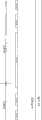
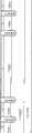
对功率MOSFET性能的提高更多地需要从优化工艺条件、改进器件结构方面入手。日本应用物理杂志2008年第3期介绍了一种低压N通道沟槽型功率金属氧化半导体场效应管沟槽终端区的结构及实现方法,该沟槽型功率金属氧化半导体场效应管的结构如图29所示,活动区在左边,该结构的底部是漏极末端,划片道在右端。有源区终端和划片道之间有三个沟槽,P型基区被定义为PMOS的源极或漏极,沟槽底部为PMOS的沟道,N-漂移区是PMOS基区,沟槽内填充的多晶硅是PMOS的栅极,沟槽多晶硅电连接到其左边的P型基区。To improve the performance of power MOSFET, it is more necessary to start from optimizing process conditions and improving device structure. The Japanese Journal of Applied Physics, No. 3, 2008, introduced the structure and implementation method of the trench termination region of a low-voltage N-channel trenched power metal oxide semiconductor field effect transistor. The structure of the trenched power metal oxide semiconductor field effect transistor is as follows: As shown in Figure 29, the active area is on the left, the bottom of the structure is the drain end, and the scribe lane is on the right. There are three trenches between the terminal of the active area and the scribe track, the P-type base area is defined as the source or drain of the PMOS, the bottom of the trench is the channel of the PMOS, and the N-drift area is the PMOS base area. The filled polysilicon is the gate of the PMOS, and the trench polysilicon is electrically connected to the P-type base region on its left.
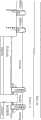
图30为美国专利文件US20080227269A1公开的另一种沟槽型功率金属氧化半导体场效应管的结构及实现方法,包括有源区10、终端区12、栅极沟槽14、基区16、漂移区18、薄氧化物20、厚氧化物22、源区26、接触孔区28、外延层31、衬底32、较厚氧化物40,以及源极(接触)金属等,在制备过程中,其基区是在沟槽掩模之前,在外延层上制成,省略了基区掩模,利用源区掩模,注入掺杂物,形成源区。Fig. 30 shows the structure and implementation method of another trench type power metal oxide semiconductor field effect transistor disclosed in the US patent document US20080227269A1, including an active region 10, a
上述结构(图29和图30)的沟槽型功率金属氧化半导体场效应管,其制备工艺虽然也少用基区掩模形成P型基区,但需要N+源区掩模版形成NMOS的源区,制造工序较多,器件的质量和可靠性相对较差。For the trench type power metal oxide semiconductor field effect transistor with the above structure (Figure 29 and Figure 30), although the manufacturing process rarely uses a base area mask to form a P-type base area, it needs an N+ source area mask to form an NMOS source area , There are many manufacturing processes, and the quality and reliability of the device are relatively poor.
发明内容Contents of the invention
为了解决现有技术存在的不足,本发明提供一种沟槽型半导体功率器件及其制备方法,减少了制造沟槽型半导体功率器件工序,避免了有关工序造成的污染,提高了器件的质量和可靠性,同时减少成本和制造时间。In order to solve the deficiencies in the prior art, the present invention provides a trench type semiconductor power device and its preparation method, which reduces the manufacturing process of the trench type semiconductor power device, avoids the pollution caused by the related process, and improves the quality and quality of the device. reliability while reducing cost and manufacturing time.
为了实现上述目的,根据本发明的一种沟槽型半导体功率器件的制备方法,该方法包括以下步骤:In order to achieve the above object, according to a method for preparing a trench type semiconductor power device of the present invention, the method comprises the following steps:
首先,利用沟槽掩模对衬底上的外延层进行侵蚀而形成多个栅极沟槽,并注入掺杂剂分别形成源区和基区;First, using a trench mask to etch the epitaxial layer on the substrate to form a plurality of gate trenches, and injecting dopants to form a source region and a base region respectively;
然后,利用接触孔掩模,对层间介质进行侵蚀形成接触沟槽,并对接触沟槽进行填充形成沟槽插塞;Then, using the contact hole mask, the interlayer dielectric is etched to form a contact trench, and the contact trench is filled to form a trench plug;
最后,利用金属掩模进行金属侵蚀,形成金属垫层和连线。Finally, metal etching is performed using a metal mask to form a metal pad layer and wiring.
进一步地,所述制备方法还包括以下步骤:Further, the preparation method also includes the following steps:
1)利用沟槽掩模将暴露的氧化层干蚀掉;1) using a trench mask to dry-etch the exposed oxide layer;
2)注入N型掺杂剂,并采用退火作业将其推进扩散到外延层形成源区;2) Implanting N-type dopant, and using annealing operation to advance and diffuse it to the epitaxial layer to form the source region;
3)将外延层开出沟槽,去掉氧化层;3) Grooving the epitaxial layer and removing the oxide layer;
4)对沟槽进行牺牲性处理,并填充沟槽;4) Perform sacrificial treatment on the trench and fill the trench;
5)注入P型掺杂物形成基区,并采用退火作业将基区推进扩散到外延层中;5) Implanting P-type dopants to form a base region, and using annealing operation to advance and diffuse the base region into the epitaxial layer;
6)在最顶层形成层间介质,并利用接触孔掩模形成接触沟槽;6) forming an interlayer dielectric on the topmost layer, and using a contact hole mask to form a contact trench;
7)对接触沟槽进行填充形成沟槽插塞;7) filling the contact trench to form a trench plug;
8)在层间介质上沉积一层铝铜合金,并利用金属掩模进行金属侵蚀形成金属垫层和连线。8) Depositing a layer of aluminum-copper alloy on the interlayer dielectric, and using a metal mask to perform metal erosion to form a metal pad layer and wiring.
进一步地,所述制备方法还包括以下步骤:Further, the preparation method also includes the following steps:
1)利用沟槽掩模将暴露的氧化层干蚀掉;1) using a trench mask to dry-etch the exposed oxide layer;
2)将外延层开出沟槽,去掉氧化层;2) Grooving the epitaxial layer and removing the oxide layer;
3)对沟槽进行牺牲性处理,并填充沟槽;3) Perform sacrificial treatment on the trench and fill the trench;
4)注入P型掺杂物形成基区,并采用退火作业将P型基区推进扩散到外延层中;4) Implanting P-type dopants to form a base region, and annealing is used to advance and diffuse the P-type base region into the epitaxial layer;
5)将N型掺杂剂注入P型基区形成源区,并采用退火作业将N型源区推进扩散到P型基区中;5) injecting N-type dopants into the P-type base region to form a source region, and annealing to advance and diffuse the N-type source region into the P-type base region;
6)在最顶层形成层间介质,并利用接触孔掩模形成接触沟槽;6) forming an interlayer dielectric on the topmost layer, and using a contact hole mask to form a contact trench;
7)对接触沟槽进行填充形成沟槽插塞;7) filling the contact trench to form a trench plug;
8)在层间介质上沉积一层铝铜合金,并利用金属掩模进行金属侵蚀形成金属垫层和连线。8) Depositing a layer of aluminum-copper alloy on the interlayer dielectric, and using a metal mask to perform metal erosion to form a metal pad layer and wiring.
更进一步地,注入N型掺杂剂是直接透过氧化层向外延层或透过栅极氧化层向P型基区直接注入N型掺杂剂;注入P型掺杂剂是直接透过栅极氧化层向外延层注入P型掺杂剂。這些步骤都省去生成氧化层,通过源区/基区掩模暴露及蝕掉氧化层,才做掺杂剂注入的工序。Furthermore, injecting N-type dopants is directly injecting N-type dopants into the epitaxial layer through the oxide layer or directly injecting N-type dopants into the P-type base region through the gate oxide layer; injecting P-type dopants directly through the gate The extreme oxide layer implants P-type dopants into the epitaxial layer. These steps all omit the process of forming an oxide layer, exposing and etching the oxide layer through the source region/base region mask, and then performing dopant implantation.
为了实现上述目的,根据本发明的一种沟槽型半导体功率器件,其特征在于,所述沟槽型半导体功率器件采用上述制备方法生产。In order to achieve the above object, a trench type semiconductor power device according to the present invention is characterized in that the trench type semiconductor power device is produced by the above preparation method.
本发明具有明显的优点和积极效果,采用本发明的制备方法,减少了利用源区掩模以及基区掩模的工序而可以直接注入形成源区和基区,实现了用较少的制备工序,完成了新结构器件的制备,使器件的质量以及可靠性得到了较大的提高;同时,由于本发明所述的制备方法中省去了生成一氧化层和蚀刻氧化层的步骤,减少了对环境的污染。The present invention has obvious advantages and positive effects. By adopting the preparation method of the present invention, the process of using the source area mask and the base area mask is reduced, and the source area and the base area can be directly implanted to form the source area and the base area. , completed the preparation of the new structure device, the quality and reliability of the device have been greatly improved; at the same time, because the preparation method of the present invention omits the steps of generating an oxide layer and etching the oxide layer, reducing the pollution of the environment.
附图说明Description of drawings
附图用来提供对本发明的进一步理解,并且构成说明书的一部分,与本发明的实施例一起用于解释本发明,并不构成对本发明的限制。在附图中:The accompanying drawings are used to provide a further understanding of the present invention, and constitute a part of the description, and are used together with the embodiments of the present invention to explain the present invention, and do not constitute a limitation to the present invention. In the attached picture:
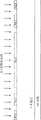
图1为根据本发明的沟槽型半导体功率器件制备方法中暴露氧化层示意图;Fig. 1 is a schematic diagram of an exposed oxide layer in a method for preparing a trench type semiconductor power device according to the present invention;
图2为根据本发明的沟槽型半导体功率器件制备方法中暴露外延层示意图;Fig. 2 is a schematic diagram of the exposed epitaxial layer in the preparation method of the trench type semiconductor power device according to the present invention;
图3为根据本发明的沟槽型半导体功率器件制备方法实施例1中不使用源区掩模注入N型掺杂剂示意图;3 is a schematic diagram of implanting N-type dopants without using a source region mask in
图4为根据本发明的沟槽型半导体功率器件制备方法实施例1中N型源区形成示意图;4 is a schematic diagram of forming an N-type source region in Example 1 of the method for manufacturing a trench-type semiconductor power device according to the present invention;
图5为根据本发明的沟槽型半导体功率器件制备方法实施例1中栅极沟槽形成示意图;5 is a schematic diagram of forming a gate trench in Example 1 of the method for manufacturing a trench-type semiconductor power device according to the present invention;
图6为根据本发明的沟槽型半导体功率器件制备方法实施例1中去掉氧化层示意图;6 is a schematic diagram of removing the oxide layer in
图7为根据本发明的沟槽型半导体功率器件制备方法实施例1中生成栅极氧化层示意图;7 is a schematic diagram of forming a gate oxide layer in
图8为根据本发明的沟槽型半导体功率器件制备方法实施例1中多晶硅栅极形成示意图;8 is a schematic diagram of forming a polysilicon gate in Example 1 of the method for manufacturing a trench type semiconductor power device according to the present invention;
图9为根据本发明的沟槽型半导体功率器件制备方法实施例1中不使用基区掩模注入P型掺杂剂示意图;9 is a schematic diagram of implanting P-type dopants without using a base region mask in
图10为根据本发明的沟槽型半导体功率器件制备方法实施例1中形成P型基区示意图;10 is a schematic diagram of forming a P-type base region in
图11为根据本发明的沟槽型半导体功率器件制备方法实施例1中层间介质形成示意图;11 is a schematic diagram of forming an interlayer dielectric in Example 1 of the method for manufacturing a trench-type semiconductor power device according to the present invention;
图12为根据本发明的沟槽型半导体功率器件制备方法实施例1中接触沟槽形成示意图;12 is a schematic diagram of forming a contact trench in Example 1 of the method for manufacturing a trench-type semiconductor power device according to the present invention;
图13为根据本发明的沟槽型半导体功率器件制备方法实施例1中沟槽插塞形成示意图;13 is a schematic diagram of the formation of trench plugs in Example 1 of the method for manufacturing a trench-type semiconductor power device according to the present invention;
图14为根据本发明的沟槽型半导体功率器件制备方法实施例1中金属垫层和金属连线形成示意图;14 is a schematic diagram of the formation of a metal pad layer and a metal connection in Example 1 of the method for manufacturing a trench type semiconductor power device according to the present invention;
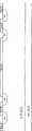
图15为根据本发明的沟槽型半导体功率器件制备方法实施例2中栅极沟槽形成示意图;15 is a schematic diagram of gate trench formation in Example 2 of the method for manufacturing a trench-type semiconductor power device according to the present invention;
图16为根据本发明的沟槽型半导体功率器件制备方法实施例2中去除氧化层示意图;16 is a schematic diagram of removing an oxide layer in Embodiment 2 of the method for manufacturing a trench type semiconductor power device according to the present invention;
图17为根据本发明的沟槽型半导体功率器件制备方法实施例2中生成栅极氧化层示意图;17 is a schematic diagram of forming a gate oxide layer in Embodiment 2 of the method for manufacturing a trench type semiconductor power device according to the present invention;
图18为根据本发明的沟槽型半导体功率器件制备方法实施例2中多晶硅栅极形成示意图;18 is a schematic diagram of forming a polysilicon gate in Example 2 of the method for manufacturing a trench type semiconductor power device according to the present invention;
图19为根据本发明的沟槽型半导体功率器件制备方法实施例2中不使用基区掩模注入P型掺杂剂示意图;19 is a schematic diagram of implanting P-type dopants without using a base region mask in Example 2 of the method for manufacturing a trench type semiconductor power device according to the present invention;
图20为根据本发明的沟槽型半导体功率器件制备方法实施例2中P型基区形成示意图;20 is a schematic diagram of the formation of a P-type base region in Embodiment 2 of the method for manufacturing a trench-type semiconductor power device according to the present invention;
图21为根据本发明的沟槽型半导体功率器件制备方法实施例2中不使用源区掩模注入N型掺杂剂示意图;21 is a schematic diagram of implanting N-type dopants without using a source region mask in Embodiment 2 of the method for manufacturing a trench type semiconductor power device according to the present invention;
图22为根据本发明的沟槽型半导体功率器件制备方法实施例2中N型源区形成示意图;22 is a schematic diagram of forming an N-type source region in Example 2 of the method for manufacturing a trench-type semiconductor power device according to the present invention;
图23为根据本发明的沟槽型半导体功率器件制备方法实施例2中层间介质形成示意图;23 is a schematic diagram of forming an interlayer dielectric in Example 2 of the method for manufacturing a trench type semiconductor power device according to the present invention;
图24为根据本发明的沟槽型半导体功率器件制备方法实施例2中接触沟槽形成示意图;24 is a schematic diagram of forming a contact trench in Example 2 of the method for manufacturing a trench-type semiconductor power device according to the present invention;
图25为根据本发明的沟槽型半导体功率器件制备方法实施例2中沟槽插塞形成示意图;25 is a schematic diagram of the formation of trench plugs in Example 2 of the method for manufacturing a trench-type semiconductor power device according to the present invention;
图26为根据本发明的沟槽型半导体功率器件制备方法实施例2中金属垫层和金属连线形成示意图;26 is a schematic diagram of the formation of a metal pad layer and a metal connection in Example 2 of the method for manufacturing a trench type semiconductor power device according to the present invention;
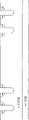
图27为根据本发明的沟槽型半导体功率器件制备方法实施例3中接触沟槽形成示意图;27 is a schematic diagram of forming a contact trench in Example 3 of the method for manufacturing a trench-type semiconductor power device according to the present invention;
图28为根据本发明的沟槽型半导体功率器件制备方法实施例4中接触沟槽形成示意图;28 is a schematic diagram of the formation of contact trenches in Embodiment 4 of the method for manufacturing a trench-type semiconductor power device according to the present invention;
图29为日本公开的一种沟槽型半导体功率器件结构示意图;Fig. 29 is a schematic structural diagram of a trench type semiconductor power device disclosed in Japan;
图30为美国公开的一种沟槽型半导体功率器件结构示意图;Fig. 30 is a schematic structural diagram of a trench type semiconductor power device disclosed in the United States;
具体实施方式Detailed ways
以下结合附图对本发明的优选实施例进行说明,应当理解,此处所描述的优选实施例仅用于说明和解释本发明,并不用于限定本发明。The preferred embodiments of the present invention will be described below in conjunction with the accompanying drawings. It should be understood that the preferred embodiments described here are only used to illustrate and explain the present invention, and are not intended to limit the present invention.
本发明的沟槽型半导体功率器件制备方法,首先,利用沟槽掩模对衬底上的外延层进行侵蚀而形成多个栅极沟槽,并注入掺杂剂分别形成源区和基区;然后,利用接触孔掩模,对层间介质进行侵蚀形成接触沟槽,并用钛或氮化钛和钨层对接触沟槽进行填充形成沟槽插塞;最后,利用金属掩模进行金属侵蚀,形成金属垫层和连线。In the preparation method of the trench type semiconductor power device of the present invention, first, the epitaxial layer on the substrate is etched to form a plurality of gate trenches by using a trench mask, and dopant is injected to form a source region and a base region respectively; Then, use the contact hole mask to etch the interlayer dielectric to form a contact trench, and fill the contact trench with titanium or titanium nitride and tungsten layers to form a trench plug; finally, use a metal mask to perform metal erosion, Form metal pads and connections.
实施例1Example 1
如图1所示,外延层置于衬底的上方,首先在外延层的上面采用积淀或热生长方式形成氧化层(氧化物硬光罩),在氧化层上再积淀一层光刻涂层,然后通过沟槽掩模形成图案暴露出氧化层的一些部分。As shown in Figure 1, the epitaxial layer is placed above the substrate. First, an oxide layer (oxide hard mask) is formed on the epitaxial layer by deposition or thermal growth, and then a layer of photoresist coating is deposited on the oxide layer. , and then patterned through the trench mask to expose some portions of the oxide layer.
如图2所示,对沟槽掩模形成图案暴露出的氧化层进行干蚀后,暴露出外延层,然后清除掉光刻涂层。As shown in FIG. 2 , after dry etching the oxide layer exposed by patterning the trench mask, the epitaxial layer is exposed, and then the photolithographic coating is removed.
如图3所示,省去生成一氧化层和通过源区掩模暴露和蚀刻氧化层,而透过氧化层向外延层直接被注入N型掺杂剂,而被氧化层覆盖的部分没有被注入,N型掺杂剂采用磷或砷。As shown in Figure 3, the generation of an oxide layer and the exposure and etching of the oxide layer through the source region mask are omitted, and the N-type dopant is directly implanted into the epitaxial layer through the oxide layer, and the part covered by the oxide layer is not covered. For implantation, phosphorus or arsenic is used as the N-type dopant.
如图4所示,在该处理过程中,注入的N型掺杂剂通过退火作业被推进扩散到外延层形成N型源区。N型源区的深度依赖于多种因素,决定于所采用的掺杂剂的类型、注入时的能量、浓度以及退火时间等。通过调整这些因素来实现所需的浓度和深度。As shown in FIG. 4 , during this process, the implanted N-type dopant is propelled and diffused into the epitaxial layer to form an N-type source region through an annealing operation. The depth of the N-type source region depends on many factors, such as the type of dopant used, the energy, concentration and annealing time during implantation. Achieve the desired concentration and depth by adjusting these factors.
如图5所示,N型源区通过蚀刻形成沟槽,该沟槽穿过N型源区延伸至外延层。As shown in FIG. 5 , the N-type source region is etched to form a trench, and the trench extends through the N-type source region to the epitaxial layer.
如图6所示,在形成沟槽后,去掉氧化层,暴露出N型源区和外延层。As shown in FIG. 6, after the trench is formed, the oxide layer is removed to expose the N-type source region and the epitaxial layer.
如图7所示,对沟槽进行牺牲性氧化,以消除在开槽过程中被等离子破坏的硅层,并通过热生长的方式,在沟槽暴露着的侧壁和底部,以及N型源区和外延层的上表面形成一层薄的栅极氧化层。As shown in Figure 7, sacrificial oxidation is performed on the trench to eliminate the silicon layer damaged by the plasma during the trenching process, and through thermal growth, the exposed sidewalls and bottom of the trench, as well as the N-type source A thin gate oxide layer is formed on the upper surface of the epitaxial region and the epitaxial layer.
如图8所示,在沟槽中沉积一层已掺杂的多晶硅(含有掺杂剂的多晶硅),以填充沟槽并覆盖顶面,接着对多晶硅层进行化学机械抛光。As shown in FIG. 8 , a layer of doped polysilicon (polysilicon containing dopants) is deposited in the trench to fill the trench and cover the top surface, followed by chemical mechanical polishing of the polysilicon layer.
如图9所示,省去生成一氧化层和通过基区掩模暴露和蚀刻氧化层,而直接透过栅极氧化层向外延层注入P型掺杂剂,在外延层上形成P型基区。As shown in Figure 9, the generation of an oxide layer and the exposure and etching of the oxide layer through the base region mask are omitted, and the P-type dopant is directly injected into the epitaxial layer through the gate oxide layer to form a P-type base layer on the epitaxial layer. district.
如图10所示,通过退火处理,使P型基区推進扩散到外延层中。P型基区的深度依赖于多种因素,決定于所采用的掺杂剂的类型、注入时的能量、浓度以及退火时间等。通过调整这些因素来实现所需的浓度和深度。As shown in FIG. 10 , the P-type base region is promoted and diffused into the epitaxial layer through annealing treatment. The depth of the P-type base region depends on many factors, such as the type of dopant used, the energy, concentration and annealing time during implantation. Achieve the desired concentration and depth by adjusting these factors.
如图11所示,为了在上述P型基区和N型源区形成接触孔沟槽,在最顶层沉积硼磷玻璃和二氧化硅形成层间介质。As shown in FIG. 11 , in order to form contact hole trenches in the above-mentioned P-type base region and N-type source region, boron-phosphorus glass and silicon dioxide are deposited on the top layer to form an interlayer dielectric.
如图12所示,通过接触孔掩模,对层间介质进行浸蚀以形成接触沟槽;然后对含有掺杂剂的外延层进行浸蚀,使接触沟槽更深地穿过源区进入到P型基区。As shown in Figure 12, through the contact hole mask, the interlayer dielectric is etched to form a contact trench; then the epitaxial layer containing dopants is etched to make the contact trench go deeper through the source region into the P-type base region.
如图13所示,对接触沟槽进行乾蚀,並在沟槽侧壁、底部以及外延层上表面沉积一层钛/氮化钛层,再对接触沟槽进行钨填充以形成沟槽插塞,并对层间介质顶层进行浸蚀,以去除钛/氮化钛和钨。As shown in Figure 13, the contact trench is dry-etched, and a layer of titanium/titanium nitride is deposited on the side wall, bottom and upper surface of the epitaxial layer of the trench, and then the contact trench is filled with tungsten to form a trench socket. plug, and etch the top interlayer dielectric to remove titanium/titanium nitride and tungsten.
如图14所示,在该器件的上面沉积一层铝铜合金,然后通过金属掩模进行金属浸蚀,形成金属垫层和连线。As shown in Figure 14, a layer of aluminum-copper alloy is deposited on the device, and then metal etching is performed through a metal mask to form a metal pad layer and wiring.
实施例2Example 2
首先将外延层置于衬底的上方,在外延层的上面采用积淀或热生长方式形成氧化层(氧化物硬光罩),在氧化层上再积淀一层光刻涂层,然后通过沟槽掩模形成图案暴露出氧化层的一些部分;对沟槽掩模形成图案暴露出氧化层的一些部分进行干蚀后,暴露出外延层,然后清除掉光刻涂层。First, the epitaxial layer is placed above the substrate, and an oxide layer (oxide hard mask) is formed on the epitaxial layer by deposition or thermal growth, and a layer of photoresist coating is deposited on the oxide layer, and then through the trench The mask is patterned to expose portions of the oxide layer; the epitaxial layer is exposed after dry etching the portions of the trench mask patterned to expose the oxide layer, and then the photolithographic coating is removed.
如图15所示,暴露的外延层通过蚀刻形成栅极沟槽。As shown in Figure 15, the exposed epitaxial layer is etched to form gate trenches.
如图16所示,在外延层形成沟槽后,去掉氧化层,暴露出全部外延层。As shown in FIG. 16 , after trenches are formed in the epitaxial layer, the oxide layer is removed to expose the entire epitaxial layer.
如图17所示,对沟槽进行牺牲性氧化,并通过热生长的方式,在沟槽暴露着的侧壁和底部,以及外延层的上表面形成一层薄的栅极氧化层。As shown in FIG. 17 , sacrificial oxidation is performed on the trench, and a thin gate oxide layer is formed on the exposed sidewall and bottom of the trench and the upper surface of the epitaxial layer by thermal growth.
如图18所示,在沟槽中沉积一层包含掺杂剂的多晶硅,以填充沟槽并覆盖顶面,接着对多晶硅层进行化学机械抛光。As shown in FIG. 18 , a layer of polysilicon containing dopants is deposited in the trench to fill the trench and cover the top surface, followed by chemical mechanical polishing of the polysilicon layer.
如图19所示,省去生成一氧化层和通过基区掩模暴露和蚀刻氧化层,而直接透过栅极氧化层向外延层注入P型掺杂剂,在外延层上形成P型基区。As shown in Figure 19, the generation of an oxide layer and the exposure and etching of the oxide layer through the base region mask are omitted, and the P-type dopant is directly implanted into the epitaxial layer through the gate oxide layer to form a P-type base layer on the epitaxial layer. district.
如图20所示,通过退火处理,使P型基区推進扩散到外延层中。P型基区的深度依赖于多种因素,决定于所采用的掺杂剂的类型、注入时的能量、浓度以及退火时间等。通过调整这些因素来实现所需的浓度和深度。As shown in FIG. 20, the P-type base region is promoted and diffused into the epitaxial layer through annealing treatment. The depth of the P-type base region depends on many factors, such as the type of dopant used, the energy, concentration and annealing time during implantation. Achieve the desired concentration and depth by adjusting these factors.
如图21所示,省去生成一氧化层和通过源区掩模暴露和蚀刻氧化层,而直接透过栅极氧化层向P型基区注入N型掺杂剂,如磷或砷,在P型基区上形成N型源区。As shown in Figure 21, the generation of an oxide layer and the exposure and etching of the oxide layer through the source region mask are omitted, and the N-type dopant, such as phosphorus or arsenic, is directly implanted into the P-type base region through the gate oxide layer. An N-type source region is formed on the P-type base region.
如图22所示,通过退火作业,N型源区被推进扩散,增加N型源区在P型基区的深度。N型源区的深度依赖于多种因素,决定于所采用的掺杂剂的类型、注入时的能量、浓度以及退火时间等,通过调整这些因素来实现所需的浓度和深度。As shown in FIG. 22, through the annealing operation, the N-type source region is promoted and diffused, increasing the depth of the N-type source region in the P-type base region. The depth of the N-type source region depends on many factors, such as the type of dopant used, the energy, concentration and annealing time during implantation, etc., and the required concentration and depth can be achieved by adjusting these factors.
如图23所示,为了在上述P型基区和N型源区形成接触孔沟槽,在最顶层沉积硼磷玻璃和二氧化硅形成层间介质。As shown in FIG. 23 , in order to form contact hole trenches in the above-mentioned P-type base region and N-type source region, borophosphorus glass and silicon dioxide are deposited on the top layer to form an interlayer dielectric.
如图24所示,通过接触孔掩模,对层间介质进行浸蚀以形成接触沟槽;然后对含有掺杂剂的外延层进行浸蚀,使接触沟槽更深地穿过源区进入到P型基区。As shown in Figure 24, through the contact hole mask, the interlayer dielectric is etched to form a contact trench; then the epitaxial layer containing dopants is etched to make the contact trench go deeper through the source region into the P-type base region.
如图25所示,对接触沟槽进行干蚀,並在沟槽侧壁、底部以及外延层上表面沉积一层钛/氮化钛层,再对接触沟槽进行钨填充以形成沟槽插塞,并对层间介质顶层进行浸蚀,以去除钛/氮化钛和钨。As shown in Figure 25, the contact trench is dry-etched, and a layer of titanium/titanium nitride is deposited on the side wall, bottom and upper surface of the epitaxial layer of the trench, and then the contact trench is filled with tungsten to form a trench socket. plug, and etch the top interlayer dielectric to remove titanium/titanium nitride and tungsten.
如图26所示,在该器件的上面沉积一层铝铜合金,然后通过金属掩模进行金属浸蚀,形成金属垫层和连线。As shown in Figure 26, a layer of aluminum-copper alloy is deposited on the device, and then metal etching is performed through a metal mask to form a metal pad layer and wiring.
本实施例与实施例1的区别在于,实施例2是在外延层开出沟槽并在“注入P型掺杂物形成基区,并采用退火作业将基区推进扩散到外延层中”步骤之后才做N型掺杂剂注入,而其它的步骤一样。The difference between this embodiment and
实施例3Example 3
在该实施例中,其制备方法与实施例1基本相同,不同之处在于接触沟槽的形成与实施例1存在差异。In this embodiment, its preparation method is basically the same as that of
如图27所示,通过接触孔掩模,对层间介质进行浸蚀以形成接触沟槽;然后对含有掺杂剂的外延层进行浸蚀,使接触沟槽更深地穿过源区进入到P型基区,在该制备过程中,同時侵蚀掉了终端区的N型源区和部份栅极沟槽。As shown in Figure 27, through the contact hole mask, the interlayer dielectric is etched to form a contact trench; then the epitaxial layer containing dopants is etched to make the contact trench go deeper through the source region into the In the preparation process of the P-type base region, the N-type source region and part of the gate trench of the terminal region are etched away at the same time.
实施例4Example 4
在该实施例中,其制备方法与实施例2的区别在于接触沟槽的形成方式与实施例2不同。In this embodiment, the difference between its preparation method and that of embodiment 2 lies in the way of forming the contact grooves.
如图28所示,通过接触孔掩模,对层间介质进行浸蚀以形成接触沟槽;然后对含有掺杂剂的外延层进行浸蚀,使接触沟槽更深地穿过源区进入到P型基区,在该制备过程中,同時侵蚀掉了终端区的N型源区和部份栅极沟槽。As shown in Figure 28, through the contact hole mask, the interlayer dielectric is etched to form a contact trench; then the epitaxial layer containing dopants is etched to make the contact trench go deeper through the source region into the In the preparation process of the P-type base region, the N-type source region and part of the gate trench of the terminal region are etched away at the same time.
本领域普通技术人员可以理解:以上所述仅为本发明的优选实施例而已,并不用于限制本发明,本发明不排它地涉及用于制造半导体器件(例如,MOS器件或绝缘栅双极晶体管(IGBT)类型的器件或双极结型晶体管(BJT)类型的器件或双极二极管或肖特基二极管)的工艺及对应的器件。本发明的实施例是以N型通道沟槽型半导体功率器件作出說明,不排它地涉及P型通道半导体功率器件的制造,主要不同是掺杂物的类型。尽管参照前述实施例对本发明进行了详细的说明,对于本领域的技术人员来说,其依然可以对前述各实施例所记载的技术方案进行修改,或者对其中部分技术特征进行等同替换。凡在本发明的精神和原则之内,所作的任何修改、等同替换、改进等,均应包含在本发明的保护范围之内。Those of ordinary skill in the art can understand that: the above description is only a preferred embodiment of the present invention, and is not intended to limit the present invention, and the present invention does not exclusively relate to a Transistor (IGBT) type devices or bipolar junction transistor (BJT) type devices or bipolar diodes or Schottky diodes) technology and corresponding devices. The embodiment of the present invention is illustrated by an N-channel trench type semiconductor power device, not exclusively related to the manufacture of a P-type channel semiconductor power device, and the main difference is the type of dopant. Although the present invention has been described in detail with reference to the aforementioned embodiments, those skilled in the art can still modify the technical solutions described in the aforementioned embodiments, or perform equivalent replacements for some of the technical features. Any modifications, equivalent replacements, improvements, etc. made within the spirit and principles of the present invention shall be included within the protection scope of the present invention.
Claims (12)
Translated fromChinesePriority Applications (3)
| Application Number | Priority Date | Filing Date | Title |
|---|---|---|---|
| CN2010101049017ACN101777514B (en) | 2010-02-03 | 2010-02-03 | A trench type semiconductor power device and its preparation method |
| PCT/CN2010/074664WO2011094993A1 (en) | 2010-02-03 | 2010-06-29 | Trench semiconductor power device and fabrication method thereof |
| US13/576,702US20130049107A1 (en) | 2010-02-03 | 2010-06-29 | Trench semiconductor power device and fabrication method thereof |
Applications Claiming Priority (1)
| Application Number | Priority Date | Filing Date | Title |
|---|---|---|---|
| CN2010101049017ACN101777514B (en) | 2010-02-03 | 2010-02-03 | A trench type semiconductor power device and its preparation method |
Publications (2)
| Publication Number | Publication Date |
|---|---|
| CN101777514A CN101777514A (en) | 2010-07-14 |
| CN101777514Btrue CN101777514B (en) | 2012-12-05 |
Family
ID=42513913
Family Applications (1)
| Application Number | Title | Priority Date | Filing Date |
|---|---|---|---|
| CN2010101049017AActiveCN101777514B (en) | 2010-02-03 | 2010-02-03 | A trench type semiconductor power device and its preparation method |
Country Status (3)
| Country | Link |
|---|---|
| US (1) | US20130049107A1 (en) |
| CN (1) | CN101777514B (en) |
| WO (1) | WO2011094993A1 (en) |
Families Citing this family (20)
| Publication number | Priority date | Publication date | Assignee | Title |
|---|---|---|---|---|
| CN102376554B (en)* | 2010-08-23 | 2014-02-05 | 科轩微电子股份有限公司 | Trench type power semiconductor manufacturing method |
| US8507978B2 (en)* | 2011-06-16 | 2013-08-13 | Alpha And Omega Semiconductor Incorporated | Split-gate structure in trench-based silicon carbide power device |
| CN102956479B (en)* | 2011-08-24 | 2015-06-24 | 大中积体电路股份有限公司 | Insulated gate bipolar transistor structure and manufacturing method thereof |
| CN103187288B (en)* | 2011-12-29 | 2016-08-10 | 立新半导体有限公司 | A kind of preparation method of the groove semiconductor power device with electrostatic protection function |
| CN103187292B (en)* | 2011-12-29 | 2016-06-29 | 立新半导体有限公司 | A kind of method manufacturing trench semiconductor power device |
| CN103187282B (en)* | 2011-12-29 | 2016-04-13 | 立新半导体有限公司 | A kind of preparation method of groove semiconductor power device |
| CN103187291B (en)* | 2011-12-29 | 2016-02-10 | 立新半导体有限公司 | A kind of method preparing trench semiconductor power discrete device |
| CN103187287B (en)* | 2011-12-29 | 2016-08-10 | 立新半导体有限公司 | A kind of preparation method of groove discrete semiconductor device |
| CN103187281B (en)* | 2011-12-29 | 2016-04-13 | 立新半导体有限公司 | A kind of preparation method of trench semiconductor power discrete device |
| CN103219241B (en)* | 2012-01-19 | 2016-06-22 | 立新半导体有限公司 | A kind of method preparing groove discrete semiconductor device |
| JP2014078689A (en)* | 2012-09-20 | 2014-05-01 | Toshiba Corp | Power semiconductor device and method of manufacturing the same |
| TWI578403B (en)* | 2014-10-03 | 2017-04-11 | 佰群科技股份有限公司 | Trench schottky diode and manufacturing mehtod thereof |
| KR102219504B1 (en) | 2015-03-18 | 2021-02-25 | 한국전자통신연구원 | Field effect power electronic device and method for fabricating the same |
| JP6488204B2 (en)* | 2015-07-07 | 2019-03-20 | 株式会社豊田中央研究所 | Semiconductor device manufacturing method |
| CN105118857B (en)* | 2015-07-20 | 2018-12-25 | 青岛佳恩半导体有限公司 | A kind of manufacturing method of groove type power MOS FET |
| US9711394B1 (en)* | 2016-05-23 | 2017-07-18 | United Microelectronics Corp. | Method for cleaning the surface of an epitaxial layer in openings of semiconductor device |
| KR102492733B1 (en) | 2017-09-29 | 2023-01-27 | 삼성디스플레이 주식회사 | Copper plasma etching method and manufacturing method of display panel |
| CN115425079A (en)* | 2022-07-29 | 2022-12-02 | 深圳基本半导体有限公司 | A trench type double-layer gate power device and its manufacturing method |
| CN115394852A (en)* | 2022-08-05 | 2022-11-25 | 深圳基本半导体有限公司 | Structure of shielded gate power MOSFET and manufacturing method thereof |
| CN115360239A (en)* | 2022-08-05 | 2022-11-18 | 深圳基本半导体有限公司 | A shielded gate power VDMOS device and its manufacturing method |
Citations (2)
| Publication number | Priority date | Publication date | Assignee | Title |
|---|---|---|---|---|
| CN1552102A (en)* | 2001-09-05 | 2004-12-01 | Trench Field Effect Transistor with Self-Aligned Source and Contact | |
| CN101261992A (en)* | 2008-04-11 | 2008-09-10 | 苏州硅能半导体科技股份有限公司 | A power groove MOS field effect tube and its making method |
Family Cites Families (11)
| Publication number | Priority date | Publication date | Assignee | Title |
|---|---|---|---|---|
| JP4073176B2 (en)* | 2001-04-02 | 2008-04-09 | 新電元工業株式会社 | Semiconductor device and manufacturing method thereof |
| US6762445B2 (en)* | 2001-07-19 | 2004-07-13 | Matsushita Electric Industrial Co., Ltd. | DRAM memory cell with dummy lower electrode for connection between upper electrode and upper layer interconnect |
| US6800904B2 (en)* | 2002-10-17 | 2004-10-05 | Fuji Electric Co., Ltd. | Semiconductor integrated circuit device and method of manufacturing the same |
| US20060273382A1 (en)* | 2005-06-06 | 2006-12-07 | M-Mos Sdn. Bhd. | High density trench MOSFET with low gate resistance and reduced source contact space |
| US20070063269A1 (en)* | 2005-09-20 | 2007-03-22 | International Rectifier Corp. | Trench IGBT with increased short circuit capability |
| US7750398B2 (en)* | 2006-09-26 | 2010-07-06 | Force-Mos Technology Corporation | Trench MOSFET with trench termination and manufacture thereof |
| US8035159B2 (en)* | 2007-04-30 | 2011-10-11 | Alpha & Omega Semiconductor, Ltd. | Device structure and manufacturing method using HDP deposited source-body implant block |
| CN101459135B (en)* | 2007-12-14 | 2010-05-26 | 上海华虹Nec电子有限公司 | Implementing method for slot type dual layer grid power MOS device construction |
| CN101488521A (en)* | 2008-01-16 | 2009-07-22 | 力士科技股份有限公司 | Trench MOS transistor structure and process thereof |
| US8222108B2 (en)* | 2009-07-08 | 2012-07-17 | Force Mos Technology Co., Ltd. | Method of making a trench MOSFET having improved avalanche capability using three masks process |
| US20110006362A1 (en)* | 2009-07-10 | 2011-01-13 | Force Mos Technology Co. Ltd. | Trench MOSFET with on-resistance reduction |
- 2010
- 2010-02-03CNCN2010101049017Apatent/CN101777514B/enactiveActive
- 2010-06-29WOPCT/CN2010/074664patent/WO2011094993A1/enactiveApplication Filing
- 2010-06-29USUS13/576,702patent/US20130049107A1/ennot_activeAbandoned
Patent Citations (2)
| Publication number | Priority date | Publication date | Assignee | Title |
|---|---|---|---|---|
| CN1552102A (en)* | 2001-09-05 | 2004-12-01 | Trench Field Effect Transistor with Self-Aligned Source and Contact | |
| CN101261992A (en)* | 2008-04-11 | 2008-09-10 | 苏州硅能半导体科技股份有限公司 | A power groove MOS field effect tube and its making method |
Also Published As
| Publication number | Publication date |
|---|---|
| CN101777514A (en) | 2010-07-14 |
| US20130049107A1 (en) | 2013-02-28 |
| WO2011094993A1 (en) | 2011-08-11 |
Similar Documents
| Publication | Publication Date | Title |
|---|---|---|
| CN101777514B (en) | A trench type semiconductor power device and its preparation method | |
| CN102768994B (en) | Integration of schottky diode within power MOSFET | |
| CN101834142B (en) | A kind of trench with thick insulating bottom and its semiconductor device manufacturing method | |
| TWI521604B (en) | Semiconductor component and preparation method | |
| CN102789987B (en) | Method for manufacturing super junction power transistor with low miller capacitance | |
| CN103094324B (en) | Trench-type insulated gate bipolar transistor and preparation method thereof | |
| CN113053738A (en) | Split gate type groove MOS device and preparation method thereof | |
| CN113964038B (en) | Fabrication method of trench gate MOSFET device | |
| CN105655402A (en) | Low-voltage super-junction MOSFET (metal-oxide-semiconductor field effect transistor) terminal structure and method for manufacturing same | |
| CN103632964A (en) | Method of preparing groove semiconductor power device | |
| TW563244B (en) | Deep trench isolation structure of high voltage device and its manufacturing method | |
| CN112820645A (en) | Power semiconductor device and preparation method thereof | |
| CN103839999A (en) | Structure and preparation method of power field effect transistor | |
| CN102034708B (en) | Manufacturing method of trench DMOS (double-diffused metal oxide semiconductor) transistor | |
| CN114883185A (en) | Manufacturing method of IGBT chip with high current density | |
| CN102005472B (en) | Manufacturing method of power semiconductor device | |
| CN113257674A (en) | Diode chip structure and manufacturing method | |
| CN109119473B (en) | Transistor and manufacturing method thereof | |
| CN104701169A (en) | Manufacturing technology method for anti-latch-up groove type insulated gate bipolar transistor | |
| CN104425247A (en) | Preparation method of insulated gate bipolar transistor | |
| TWI517393B (en) | Semiconductor device and method of fabricating the same | |
| CN101246825A (en) | Silicon material high frequency low power consumption power junction field effect transistor (JFET) manufacturing method | |
| KR20100074503A (en) | Trench gate mosfet and method for fabricating of the same | |
| CN100395876C (en) | Method for manufacturing power metal oxide semiconductor field effect transistor | |
| CN110197791A (en) | Trench MOSFET structure and preparation method thereof of the polysilicon as source region |
Legal Events
| Date | Code | Title | Description |
|---|---|---|---|
| C06 | Publication | ||
| PB01 | Publication | ||
| C10 | Entry into substantive examination | ||
| SE01 | Entry into force of request for substantive examination | ||
| C14 | Grant of patent or utility model | ||
| GR01 | Patent grant |