CN101770817A - Multi-interface memory verification system based on FPGA - Google Patents
Multi-interface memory verification system based on FPGADownload PDFInfo
- Publication number
- CN101770817A CN101770817ACN201010022919ACN201010022919ACN101770817ACN 101770817 ACN101770817 ACN 101770817ACN 201010022919 ACN201010022919 ACN 201010022919ACN 201010022919 ACN201010022919 ACN 201010022919ACN 101770817 ACN101770817 ACN 101770817A
- Authority
- CN
- China
- Prior art keywords
- memory
- data
- interface
- fpga
- control
- Prior art date
- Legal status (The legal status is an assumption and is not a legal conclusion. Google has not performed a legal analysis and makes no representation as to the accuracy of the status listed.)
- Pending
Links
- 230000015654memoryEffects0.000titleclaimsabstractdescription92
- 238000012795verificationMethods0.000titleclaimsabstractdescription15
- 238000004891communicationMethods0.000claimsabstractdescription16
- 238000013507mappingMethods0.000claimsabstractdescription11
- 230000001360synchronised effectEffects0.000claimsabstractdescription8
- 230000006870functionEffects0.000claimsdescription11
- 230000002093peripheral effectEffects0.000claimsdescription6
- 230000005055memory storageEffects0.000claims2
- 238000004088simulationMethods0.000claims1
- 238000012360testing methodMethods0.000abstractdescription11
- 238000000034methodMethods0.000abstractdescription9
- 238000004904shorteningMethods0.000abstract1
- 238000002054transplantationMethods0.000abstract1
- 238000010586diagramMethods0.000description9
- 230000010354integrationEffects0.000description3
- 230000007246mechanismEffects0.000description3
- 230000008569processEffects0.000description3
- 230000000630rising effectEffects0.000description3
- 238000006243chemical reactionMethods0.000description2
- 238000012545processingMethods0.000description2
- 230000006399behaviorEffects0.000description1
- 230000002457bidirectional effectEffects0.000description1
- 230000008859changeEffects0.000description1
- 230000007812deficiencyEffects0.000description1
- 238000011161developmentMethods0.000description1
- 238000005516engineering processMethods0.000description1
- 238000011990functional testingMethods0.000description1
- 238000004519manufacturing processMethods0.000description1
- 230000008520organizationEffects0.000description1
- 238000011160researchMethods0.000description1
- 238000000926separation methodMethods0.000description1
- 230000008054signal transmissionEffects0.000description1
- 238000010998test methodMethods0.000description1
- 239000002699waste materialSubstances0.000description1
Images


Landscapes
- Logic Circuits (AREA)
Abstract
Translated fromChinese
Description
Translated fromChinese技术领域technical field
本发明涉及通信技术、自动控制及仪器仪表技术领域,具体地说是一种集多种存储器的驱动及测试于一体的基于现场可编程门阵列(FPGA)的多接口存储器验证系统。The invention relates to the technical fields of communication technology, automatic control and instrumentation, in particular to a field-programmable gate array (FPGA)-based multi-interface memory verification system integrating drive and test of various memories.
背景技术Background technique
随着市场上不断推出大容量、高速度的存储器,但容量和速度的提高导致了存储器与标准接口的细节差异,新型存储器的推出从根本上改变了存储器的访问接口及对其进行访问的操作方式,市场主流控制器并不能完全支持对这样大容量、高速度并拥有特殊访问接口的存储器进行直接访问操作。With the introduction of large-capacity and high-speed memories on the market, the increase in capacity and speed has led to differences in the details of the memory and the standard interface. The introduction of new types of memory has fundamentally changed the access interface of the memory and the operation of accessing it. However, mainstream controllers in the market cannot fully support direct access operations to such large-capacity, high-speed memories with special access interfaces.
当前国内外存储器的主流测试方式仍是针对单一型号或者单一接口的芯片进行单独测试,对于不同接口类型的芯片(比如说NOR Flash和SPI Flash)来说并没有一个可通用的测试平台,这导致针对不同功能的存储芯片来说需要为其功能完整性和性能稳定性的测试提供不同的测试平台,造成资源浪费。At present, the mainstream test method of memory at home and abroad is still to test a chip of a single model or a single interface separately. There is no universal test platform for chips of different interface types (such as NOR Flash and SPI Flash), which leads to For memory chips with different functions, it is necessary to provide different test platforms for testing their functional integrity and performance stability, resulting in waste of resources.
此外,国内的研究也多停留在如何控制较传统的单一类型的存储器上,对于多种新型接口的存储器的投入实际应用的过程不利,另一方面,在基于FPGA的开发中,人们多习惯于使用FPGA芯片内嵌的仿CPU软硬核资源来完成CPU端的诸多控制工作,这些资源由于受到内部时钟的限制,无法完整的模拟出高速存储器可能的实际使用环境,不能完整测试出其工作于高速时钟下的性能。In addition, the domestic research also mostly stays on how to control the traditional single type of memory, which is not good for the process of putting the memory of various new interfaces into practical application. On the other hand, in the development based on FPGA, people are more accustomed to Use the imitation CPU soft and hard core resources embedded in the FPGA chip to complete many control tasks on the CPU side. Due to the limitation of the internal clock, these resources cannot completely simulate the possible actual use environment of the high-speed memory, and cannot fully test that it works at high speed. performance under the clock.
发明内容Contents of the invention
本发明的目的是针对现有技术的不足而提供的一种基于FPGA的多接口存储器验证系统,为存储芯片生产厂商提供了灵活简便的存储芯片功能验证及演示的平台。The purpose of the present invention is to provide a FPGA-based multi-interface memory verification system for the deficiencies of the prior art, and provide a flexible and convenient memory chip function verification and demonstration platform for memory chip manufacturers.
本发明的目的是这样实现的:The purpose of the present invention is achieved like this:
一种基于FPGA的多接口存储器验证系统,其特点是:An FPGA-based multi-interface memory verification system is characterized by:
a、系统包括高级精简指令集计算机模块(ARM模块)和现场可编程门阵列模块(FPGA模块),两模块之间以总线方式连接;采用FPGA端模拟SRAM外部存储器的方式,将FPGA内控制器逻辑映射到ARM内存中来提供数据和控制的访问接口;a. The system includes an Advanced Reduced Instruction Set Computer Module (ARM module) and a Field Programmable Gate Array module (FPGA module). The two modules are connected by a bus; the FPGA end is used to simulate the SRAM external memory, and the FPGA internal controller Logically mapped to ARM memory to provide data and control access interface;
b、系统采用异步总线通讯方式,将ARM输出的异步控制信号、异步地址及数据信号同步到FPGA的内部时钟域中;b. The system adopts asynchronous bus communication mode to synchronize the asynchronous control signal, asynchronous address and data signal output by ARM to the internal clock domain of FPGA;
c、系统存储器数据、控制接口统一采用存储器数据直接映射方式,使各存储器控制器IP核移植集成于系统中;数据访问接口以先进先出(FIFO)形式实现;c. The system memory data and control interface uniformly adopt the memory data direct mapping method, so that the IP core of each memory controller is transplanted and integrated in the system; the data access interface is realized in the form of first-in-first-out (FIFO);
其中:in:
所述ARM模块为系统控制器并外设部分配置:同步动态随机存取存储器(SDRAM)、Nand Flash内存、NOR Flash内存、通用异步接收/发送装置(UART)、USB主设备、USB设备、以太网接口、LCD接口及SD卡读卡器;The ARM module is a system controller and peripheral part configuration: Synchronous Dynamic Random Access Memory (SDRAM), Nand Flash memory, NOR Flash memory, Universal Asynchronous Receiver/Transmitter (UART), USB master device, USB device, Ethernet Network interface, LCD interface and SD card reader;
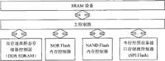
所述FPGA模块内部逻辑分为三层:与ARM接口的SRAM设备层、负责模块的控制、数据与寄存器映射的主控制器层以及存储器控制器层。The internal logic of the FPGA module is divided into three layers: an SRAM device layer interfaced with the ARM, a master controller layer responsible for module control, data and register mapping, and a memory controller layer.
上述与ARM接口的SRAM设备层通过模拟一个SRAM外部存储器向ARM提供读写接口,以此建立ARM-FPGA之间的通讯;SRAM设备层内由三个子层组成,分别为:物理子层、控制子层及用户子层。The above-mentioned SRAM device layer interfaced with ARM provides a read-write interface to ARM by simulating an SRAM external memory, so as to establish communication between ARM-FPGA; the SRAM device layer consists of three sub-layers, namely: physical sub-layer, control sublayer and user sublayer.
上述负责模块的控制、数据与寄存器映射的主控制器层转换地址、命令的格式并转发数据,并在其内部将SRAM设备层的请求转发到功能寄存器(SFR)。The above-mentioned main controller layer responsible for module control, data and register mapping converts addresses, command formats and forwards data, and internally forwards the request of the SRAM device layer to the function register (SFR).
上述存储器控制器层由四个具体的存储器控制器组成,分别是:双倍速率同步动态随机存储器(DDR SDRAM)、NOR Flash内存、NAND Flash内存以及串行外设接口内存(SPI Flash),各存储器控制器的用户访问接口各不相同,通过主控制器层进行地址、命令、数据协调控制,并向SFR控制模块提供功能控制接口。The above memory controller layer is composed of four specific memory controllers, namely: double rate synchronous dynamic random access memory (DDR SDRAM), NOR Flash memory, NAND Flash memory and serial peripheral interface memory (SPI Flash), each The user access interfaces of the memory controller are different, and the address, command, and data coordination control are carried out through the main controller layer, and the function control interface is provided to the SFR control module.
上述物理子层提供SRAM接口,将异步地址、数据同步到内部时钟,向控制子层发送访问请求信号;控制子层将物理子层传来的地址、命令及数据转换为合适的格式并放入用户子层的先进先出(FIFO),并向系统控制器发送访问请求信号;用户子层向系统控制器提供一个统一的数据、命令访问接口。The above physical sublayer provides SRAM interface, synchronizes the asynchronous address and data to the internal clock, and sends an access request signal to the control sublayer; the control sublayer converts the address, command and data from the physical sublayer into a suitable format and puts it into The first-in-first-out (FIFO) of the user sublayer sends an access request signal to the system controller; the user sublayer provides a unified data and command access interface to the system controller.
本验证系统配备市场常见的存储器接口,可以进行常规的功能测试及演示,同时,又能灵活地通过固件升级来支持最新接口类型的存储器,在最短的时间内对最新的存储器芯片进行测试、验证以及同时进行多种类型的芯片测试及演示,大大缩短了新型存储芯片投入实际使用的时间周期。This verification system is equipped with common memory interfaces in the market, and can perform routine functional tests and demonstrations. At the same time, it can flexibly support the latest interface types of memory through firmware upgrades, and test and verify the latest memory chips in the shortest time. As well as conducting multiple types of chip tests and demonstrations at the same time, the time period for new memory chips to be put into practical use is greatly shortened.
附图说明Description of drawings
图1为本发明结构示意图Fig. 1 is a structural representation of the present invention
图2为本发明ARM模块内存分布图Fig. 2 is ARM module internal memory distribution figure of the present invention
图3为本发明FPGA模块内部架构框图Fig. 3 is a block diagram of the FPGA module internal architecture of the present invention
图4为本发明FPGA模块的SRAM设备层内部框图Fig. 4 is the internal block diagram of the SRAM device layer of the FPGA module of the present invention
图5为总线通讯中数据线三态控制的IOBUF元件原理图Figure 5 is a schematic diagram of the IOBUF component of the three-state control of the data line in the bus communication
图6为本发明ARM模块与FPGA模块的数据、控制访问接口框图Fig. 6 is the data of the present invention ARM module and FPGA module, control access interface block diagram
具体实施方式Detailed ways
本发明由两大模块组成:ARM模块与FPGA模块。两模块之间以总线方式(FPGA端仿SRAM存储器)连接,采用FPGA端模拟SRAM外部存储器的方式,将FPGA内控制器逻辑映射到ARM内存中来提供数据和控制的访问接口。由于各种存储器的访问特性不同,所以ARM与FPGA通讯部分采用了全总线连接,即所有的数据线、地址线、控制线全部连接到FPGA。如图1所示的系统总体架构图。The invention consists of two modules: ARM module and FPGA module. The two modules are connected by a bus (the FPGA end imitates SRAM memory), and the FPGA end simulates the SRAM external memory, and the FPGA internal controller logic is mapped to the ARM memory to provide data and control access interfaces. Because the access characteristics of various memories are different, the ARM and FPGA communication part adopts a full bus connection, that is, all data lines, address lines, and control lines are all connected to FPGA. The overall architecture of the system shown in Figure 1.
(1)、ARM模块(1), ARM module
ARM模块采用三星S3C2440Mobile MCU作为系统控制器,此MCU基于M920T核心,拥有丰富的片内外设,支持EBI(External Bus Interface),为FPGA通讯提供了条件。能够运行Linux和Windows CE操作系统,为整个验证系统提供流行的应用平台支持。外部总线接口(EBI)总共分为8个Bank,其中Bank1、Bank2、Bank3作为外部存储器内存访问映射,提供统一的存储器访问接口。如图2所示的ARM模块内存分布图。The ARM module uses Samsung S3C2440Mobile MCU as the system controller. This MCU is based on the M920T core, has rich on-chip peripherals, supports EBI (External Bus Interface), and provides conditions for FPGA communication. It can run Linux and Windows CE operating systems, providing popular application platform support for the entire verification system. The external bus interface (EBI) is divided into 8 Banks in total, among which Bank1, Bank2, and Bank3 are used as external memory memory access mappings to provide a unified memory access interface. The memory distribution diagram of the ARM module shown in Figure 2.
(2)、FPGA模块(2), FPGA module
FPGA模块采用的是Xilinx公司的Virtex-5LX系列芯片(Virtex-5XC5VLX50),内部的实现逻辑可分为三层,分别为:与ARM接口的SRAM设备层,负责整体模块系统的控制、数据与寄存器映射的模块控制器层以及存储器控制器层。如图3所示的FPGA模块内部架构框图。The FPGA module uses Xilinx's Virtex-5LX series chip (Virtex-5XC5VLX50). The internal implementation logic can be divided into three layers, namely: the SRAM device layer interfaced with ARM, which is responsible for the control, data and registers of the overall module system Mapped module controller layer and memory controller layer. The block diagram of the internal architecture of the FPGA module as shown in Figure 3.
i、SRAM设备层i. SRAM device layer
SRAM设备层负责与ARM之间的通讯,通过模拟一个SRAM外部存储器向ARM提供读写接口,以此来建立ARM-FPGA间的通讯,图4为SRAM设备层IP内部结构框图。SRAM设备层内部由三个子层组成:物理子层,控制子层,用户子层。物理子层负责硬件链路方面的转换,提供SRAM接口,将异步地址、数据同步到内部时钟,并向控制子层发送访问请求信号。控制子层负责将物理子层传来的地址、命令及数据转换为合适的格式并放入用户子层的先进先出(FIFO),同时负责向系统主控制器发送访问请求信号。用户子层内部包括3个FIFO寄存器向系统主控制器提供了一个统一的数据、命令访问接口。The SRAM device layer is responsible for the communication with the ARM, and provides a read-write interface to the ARM by simulating an SRAM external memory to establish communication between the ARM-FPGA. Figure 4 is a block diagram of the internal structure of the SRAM device layer IP. The SRAM device layer is composed of three sublayers: the physical sublayer, the control sublayer, and the user sublayer. The physical sublayer is responsible for the conversion of the hardware link, provides the SRAM interface, synchronizes the asynchronous address and data to the internal clock, and sends the access request signal to the control sublayer. The control sublayer is responsible for converting addresses, commands and data from the physical sublayer into appropriate formats and putting them into the first-in-first-out (FIFO) of the user sublayer, and is responsible for sending access request signals to the system master controller. The user sublayer includes three FIFO registers to provide a unified data and command access interface to the main controller of the system.
ii、主控制器层ii. Main controller layer
主控制器层负责FPGA内部存储器控制器的功能协调,并完成地址、命令的格式转换以及数据的转发。当SRAM设备层请求访问的地址属于寄存器Bank时,请求将不会被转发到具体存储器控制器,而是主控制器内部的SFR(Special Function Register)处理模块来实现功能设置。SFR处理模块再根据不同的访问内容来具体改变当前活动状态下的存储器控制器行为。The main controller layer is responsible for the functional coordination of the internal memory controller of the FPGA, and completes the format conversion of addresses and commands and the forwarding of data. When the address requested by the SRAM device layer belongs to the register bank, the request will not be forwarded to the specific memory controller, but the SFR (Special Function Register) processing module inside the main controller to realize the function setting. The SFR processing module then specifically changes the behavior of the memory controller in the current active state according to different access contents.
iii、存储器控制器层iii. Memory controller layer
存储器控制器层由四个具体的存储器控制器组成,分别是:双倍速率同步动态随机存储器(DDR SDRAM)、NOR Flash内存、NAND Flash内存以及串行外设接口内存(SPI Flash),各存储器控制器的用户访问接口各不相同,因此由主控制器进行地址、命令、数据协调控制,并向SFR控制模块提供了功能控制接口。The memory controller layer consists of four specific memory controllers, namely: double rate synchronous dynamic random access memory (DDR SDRAM), NOR Flash memory, NAND Flash memory and serial peripheral interface memory (SPI Flash), each memory The user access interfaces of the controllers are different, so the main controller performs the coordinated control of address, command and data, and provides the function control interface to the SFR control module.
本发明采用ARM-FPGA分离式,关键问题在于:通信信号的同步、存储器统一数据、控制接口及存储器控制器的集成。The invention adopts the ARM-FPGA separation type, and the key problems are: the synchronization of communication signals, the unified data of memory, the integration of control interface and memory controller.
①、异步总线通讯①, asynchronous bus communication
ARM的外部总线接口(EBI)所支持的SRAM总线接口为传统异步访问总线,而FPGA内部逻辑全部采用的是同步时序逻辑,需要将ARM输出的异步控制信号、异步地址及数据信号同步到FPGA的内部时钟域中来。The SRAM bus interface supported by ARM's external bus interface (EBI) is a traditional asynchronous access bus, while the internal logic of FPGA all adopts synchronous sequential logic, which needs to synchronize the asynchronous control signal, asynchronous address and data signal output by ARM to the FPGA. from the internal clock domain.
ARM端到FPGA端的SRAM总线接口中并不包含时钟信号,FPGA只能在每个内部时钟上升沿来判断外部控制信号的状态,当检测到读写信号变化时,向SRAM控制模块给出一个读写信号。具体做法如下:The SRAM bus interface from the ARM end to the FPGA end does not contain a clock signal. The FPGA can only judge the state of the external control signal at the rising edge of each internal clock. write signal. The specific method is as follows:
i)在每个时钟上升沿寄存当前外部控制信号状态。i) Register the current external control signal state at each rising edge of the clock.
always@(posedge clk0)always@(posedge clk0)
beginbegin
ctrl_oe_n_r<=ctrl_oe_n;ctrl_oe_n_r<=ctrl_oe_n;
endend
ii)使用组合逻辑判断当前外部控制信号状态和上一周期状态,当满足下降沿时序时给出内部读写请求信号。ii) Use combinational logic to judge the current external control signal state and the state of the previous cycle, and give an internal read and write request signal when the falling edge sequence is met.
assign rd_req_r=(!ctrl_oe_n&&ctrl_oe_n_r);assign rd_req_r = (!ctrl_oe_n&&ctrl_oe_n_r);
iii)当检测到内部读写请求信号时,向SRAM控制模块给出一个时钟周期长度的读写请求信号。iii) When an internal read-write request signal is detected, a read-write request signal with a length of one clock cycle is given to the SRAM control module.
always@(posedge clk0)always@(posedge clk0)
beginbegin
rd_req<=1’b0;rd_req<=1'b0;
if(rd_req_r)beginif(rd_req_r)begin
rd_req<=1’b1;rd_req<=1'b1;
endend
endend
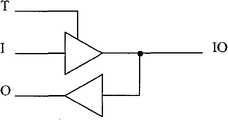
在总线通讯时还会碰到数据线的三态控制问题,解决方式为:使用FPGA内部IO模块加上三态组合控制逻辑,如图5即为总线通讯中数据线的三态控制器件IOBUF元件原理图,实现方式为:In the bus communication, the problem of three-state control of the data line will also be encountered. The solution is: use the internal IO module of the FPGA and add the three-state combination control logic, as shown in Figure 5, which is the three-state control device IOBUF component of the data line in the bus communication Schematic diagram, the implementation method is:
assign data_tri_n=(!ctrl_we_n&&ctrl_oe_n);//三态控制信号组合逻辑assign data_tri_n=(!ctrl_we_n&&ctrl_oe_n);//tri-state control signal combination logic
IOBUF u_iobuf_data //实例化一个IOBUF元件IOBUF u_iobuf_data //Instantiate an IOBUF element
(.IO(sram_data[data_i]), //sram数据总线,双向(.IO(sram_data[data_i]), //sram data bus, bidirectional
.I(rd_data[data_i]), //sram读数据总线,输入.I(rd_data[data_i]), //sram read data bus, input
.O(wr_data[data_i]), //sram写数据总线,输出.O(wr_data[data_i]), //sram write data bus, output
.T(data_tri_n) //sram数据总线,三态控制总线.T(data_tri_n) //sram data bus, tri-state control bus
););
有了经过时钟同步的地址线和数据,有了nWAIT信号来给出灵活的读写指令周期,有了数据线的三态控制,这样就在ARM和FPGA之间建立起了完善的通讯机制。With clock-synchronized address lines and data, nWAIT signal to give flexible read and write instruction cycles, and tri-state control of data lines, a perfect communication mechanism is established between ARM and FPGA.
②、存储器统一数据、控制接口②, memory unified data, control interface
为了适应各种存储器控制器的集成,为用户提供统一的应用接口,统一采用存储器数据直接映射方式,在SFR区提供特性控制接口。In order to adapt to the integration of various memory controllers and provide users with a unified application interface, the memory data direct mapping method is uniformly adopted, and the characteristic control interface is provided in the SFR area.
ARM端外部总线接口(EBI)向外扩展4个Bank总线区域给FPGA端,每个Bank有128MB空间,其中Bank1、Bank2、Bank3空间连续,这三个Bank作为统一的数据访问接口,Bank5同样拥有128MB空间,独立作为控制访问接口,提供SFR访问形式,为SFR提供一组16MB地址空间,每个加载的存储器控制器拥有独立的16MB SFR地址空间,由FPGA内SFR控制器统一控制,SFR控制器根据不同的地址映射向具体的存储器控制器转发控制请求。图6为ARM与FPGA的数据、控制访问接口框图。The external bus interface (EBI) on the ARM side expands 4 Bank bus areas to the FPGA side. Each Bank has 128MB of space, of which Bank1, Bank2, and Bank3 are continuous in space. These three Banks serve as a unified data access interface, and Bank5 also has 128MB space, independently used as a control access interface, providing SFR access form, providing a set of 16MB address space for SFR, each loaded memory controller has an independent 16MB SFR address space, which is uniformly controlled by the SFR controller in the FPGA, and the SFR controller Forward control requests to specific memory controllers according to different address mappings. Figure 6 is a block diagram of data and control access interfaces between ARM and FPGA.
③、存储器控制器的集成③, the integration of memory controller
系统提供统一的数据访问接口,方便地将存储器控制器的IP核集成到验证系统并以FIFO形式实现。数据访问FIFO分为地址/指令FIFO,写数据FIFO和读数据FIFO,地址/指令FIFO用来接收主控制器发出的读写指令以及数据访问地址,写数据FIFO接收主控制器发来的对应写指令的数据,读数据FIFO在存储器控制器接收到读指令之后,来返回从存储器读取的数据。The system provides a unified data access interface, and easily integrates the IP core of the memory controller into the verification system and realizes it in the form of FIFO. The data access FIFO is divided into address/command FIFO, write data FIFO and read data FIFO. The address/command FIFO is used to receive the read and write commands and data access addresses issued by the main controller, and the write data FIFO receives the corresponding write from the main controller. The data of the instruction, the read data FIFO returns the data read from the memory after the memory controller receives the read instruction.
主控制器要向存储器控制器发送写数据请求时,需要在写数据/指令FIFO前(或同时)将需要写的数据写入写数据FIFO,然后向数据/指令FIFO写入读写指令和写地址,在整个写操作过程中写使能信号要保持有效。主控制器要从存储器控制器读数据时,首先从数据/指令FIFO发送读指令和读地址,然后等待读信号有效,从读数据FIFO中读出需要的数据。When the main controller wants to send a write data request to the memory controller, it needs to write the data to be written into the write data FIFO before (or at the same time) the write data/command FIFO, and then write the read-write command and write to the data/command FIFO. address, the write enable signal must remain valid during the entire write operation. When the master controller wants to read data from the memory controller, it first sends a read command and a read address from the data/command FIFO, then waits for the read signal to be valid, and reads the required data from the read data FIFO.
通过主控制器向SFR控制器转发SFR访问请求,由SFR控制器理解控制器的请求的内容,再根据不同的存储器控制器特性,向下派发具体存储器控制器的功能控制请求。只有当SFR控制器判断到有效的SFR访问的内容时,才改变相应控制器IP的特性,这样各种不同的控制器IP就能避免改变大部分代码而和整个验证系统兼容,并提供能够改变其功能特性的SFR接口。The main controller forwards the SFR access request to the SFR controller, and the SFR controller understands the content of the controller's request, and then distributes the function control request of the specific memory controller downward according to the characteristics of different memory controllers. Only when the SFR controller judges the content of valid SFR access, it changes the characteristics of the corresponding controller IP, so that various controller IPs can avoid changing most of the code and be compatible with the entire verification system, and provide the ability to change Its functional characteristics of the SFR interface.
各种不同控制器在FPGA上的实现:Implementation of various controllers on FPGA:
i)DDR SDRAM控制器的实现i) Implementation of DDR SDRAM controller
在FPGA模块中通过软件使用Verilog HDL语言完成DDR SDRAM控制器的编写工作。In the FPGA module, the programming of the DDR SDRAM controller is completed by using Verilog HDL language through software.
DDR SDRAM在进行读写操作前需要进行初始化。当电平重置信号有效时,DDR SDRAM控制器就开始按照JEDEC(工业化标准组织)标准对DDR SDRAM存储器进行初始化。在完成存储器初始化之后便开始校准流程。DDR SDRAM控制器校准过程分成四个阶段,分别为DQ-DQS校准、DQS-FPGA CLK校准、读数据有效校准和DQS阀校准。DDR SDRAM needs to be initialized before reading and writing operations. When the level reset signal is valid, the DDR SDRAM controller starts to initialize the DDR SDRAM memory according to the JEDEC (Industrial Standards Organization) standard. The calibration process starts after the memory initialization is complete. The DDR SDRAM controller calibration process is divided into four stages, namely DQ-DQS calibration, DQS-FPGA CLK calibration, read data valid calibration and DQS valve calibration.
DDR SDRAM控制器的控制模块负责响应用户模块发来的读写请求,管理DDR SDRAM内部状态机,负责DDR SDRAM的物理读写指令,同时还管理DDRSDRAM的刷新机制和Bank管理机制等。DDR SDRAM有多种刷新模式,需要不断进行刷新,以保存数据。DDR SDRAM在刷新之前要求所有块必须处于空闲状态,但是实际应用中并不能保证所有块必须处于空闲状态,因此刷新之前首先对所有的块预充电,然后再刷新。The control module of the DDR SDRAM controller is responsible for responding to the read and write requests sent by the user module, managing the internal state machine of DDR SDRAM, responsible for the physical read and write instructions of DDR SDRAM, and also managing the refresh mechanism and Bank management mechanism of DDR SDRAM. DDR SDRAM has a variety of refresh modes, which need to be refreshed continuously to save data. DDR SDRAM requires that all blocks must be in an idle state before refreshing, but in practical applications, it cannot be guaranteed that all blocks must be in an idle state, so all blocks must be pre-charged before refreshing, and then refreshed.
ii)NOR Flash控制器的实现ii) Implementation of NOR Flash controller
在FPGA模块中通过软件使用Verilog HDL语言完成NOR Flash控制器的编写工作。In the FPGA module, the programming of the NOR Flash controller is completed by using Verilog HDL language through software.
对NOR Flash操作模式的控制主要表现为对功能寄存器中内容的操作。NOR Flash只能工作于异步模式,选择FIFO寄存器作为NOR Flash控制器中的数据缓存区。The control of the NOR Flash operation mode is mainly manifested as the operation of the contents in the function register. NOR Flash can only work in asynchronous mode, and the FIFO register is selected as the data buffer area in the NOR Flash controller.
iii)NAND Flash控制器的实现iii) Implementation of NAND Flash controller
在FPGA模块中通过软件使用Verilog HDL语言完成NAND Flash控制器的编写工作。In the FPGA module, the programming of the NAND Flash controller is completed by using Verilog HDL language through software.
为了满足从NAND Flash中读取数据时的时序要求,NAND Flash控制器内部控制逻辑的时钟采用的是100MHz的时钟,对100MHz的时钟进行6分频,分频得到的NAND Flash控制信号是33.33%的占空比,即低电平时间为40ns,高电平时间为20ns,这样在数据有效至读数据控制信号的有效沿(上升沿)还留有5ns的时间余量,完全满足读取数据的时序要求。In order to meet the timing requirements when reading data from NAND Flash, the internal control logic clock of the NAND Flash controller uses a 100MHz clock, divide the 100MHz clock by 6, and the NAND Flash control signal obtained by frequency division is 33.33% The duty cycle, that is, the low level time is 40ns, and the high level time is 20ns, so there is still a time margin of 5ns from the valid data to the valid edge (rising edge) of the read data control signal, which fully meets the requirements of the read data. timing requirements.
NAND Flash控制器包含有两个数据缓存区,每个为1056个字(Word),使用双数据缓存的目的是为了保证用户总能对其中一个缓存区进行操作。使用Xilinx公司集成在Virtex-5系列FPGA芯片中Block RAM资源来实现两个数据缓存区。The NAND Flash controller contains two data buffer areas, each of which is 1056 words (Word). The purpose of using double data buffer is to ensure that users can always operate on one of the buffer areas. Use the Block RAM resource integrated in the Virtex-5 series FPGA chip by Xilinx to realize two data cache areas.
在NAND的生产及使用过程中会产生坏块,为了检测数据的可靠性,使用一种比较专用的校验-汉明码ECC。汉明码能纠正单比特错误和检测双比特错误,而且计算速度很快。During the production and use of NAND, bad blocks will be generated. In order to test the reliability of the data, a special verification-Hamming code ECC is used. Hamming codes can correct single-bit errors and detect double-bit errors, and are computationally fast.
iv)SPI Flash控制器的实现iv) Implementation of SPI Flash controller
在FPGA模块中通过软件使用Verilog HDL语言完成SPI Flash控制器的编写工作。In the FPGA module, the programming of the SPI Flash controller is completed by using Verilog HDL language through software.
SPI Flash器件工作需要串行时钟,利用FPGA的外部时钟clk作为系统的基准时钟,对其进行分频得到SPI Flash芯片工作所需要的串行时钟,仅在对SPI Flash器件进行操作时才向SPI Flash器件提供串行时钟,以避免写入或读出错误的数据,因此提供了两根控制信号:tx_enable和rx_enable,只要它们两者中有一根信号的状态在系统时钟clk的下降沿时为高,则说明接下来要对SPI Flash器件进行操作了,于是将串行时钟输出到SPI Flash器件的信号输入口,从而为SPI Flash器件的工作提供时钟。The SPI Flash device requires a serial clock to work. Use the external clock clk of the FPGA as the system's reference clock, divide it to obtain the serial clock required for the SPI Flash chip to work, and send it to the SPI only when operating the SPI Flash device. The Flash device provides a serial clock to avoid writing or reading erroneous data, so two control signals are provided: tx_enable and rx_enable, as long as the state of one of them is high at the falling edge of the system clock clk , it means that the SPI Flash device will be operated next, so the serial clock is output to the signal input port of the SPI Flash device, thereby providing a clock for the operation of the SPI Flash device.
SPI Flash的指令是通过sel、addr和wr三根控制信号来给出的,SPIFlash控制器根据这三根信号线的不同组合来获得不同的控制信号。SPIFlash控制器预先将从用户那边获得的指令和地址字节寄存起来,以便当SPIFlash控制器在状态机的控制下到达正确的工作状态时能够准确地将相应的指令字节和地址字节传输给SPI Flash器件。The instructions of SPI Flash are given by three control signals of sel, addr and wr, and the SPIFlash controller obtains different control signals according to different combinations of these three signal lines. The SPIFlash controller pre-registers the instruction and address bytes obtained from the user, so that when the SPIFlash controller reaches the correct working state under the control of the state machine, it can accurately transmit the corresponding instruction bytes and address bytes For SPI Flash devices.
本发明硬件的实现是:将ARM和FPGA模块集成在一块板上,减少了ARM与FPGA之间信号传输时的噪声影响,同时减少了所占的空间。板左上方为ARM模块,包括一片ARM芯片和两片程序存储芯片,ARM模块的系统时钟为100MHz,FPGA模块位于系统板上部的中间部分,为其提供了一片25MHz的基准时钟,通过FPGA内部的数字时钟管理(DCM)模块,可得本发明中四种存储器控制器工作状态机所需的精准时钟信号。FPGA芯片正下方即为预留的FPGA I/O口,通过使用这些预留的I/O口可以方便的对新的存储器控制器类型进行升级,从而增加本发明的适应能力。The realization of the hardware of the present invention is: the ARM and the FPGA module are integrated on one board, which reduces the noise influence during signal transmission between the ARM and the FPGA, and reduces the occupied space at the same time. The upper left of the board is the ARM module, including an ARM chip and two program memory chips. The system clock of the ARM module is 100MHz, and the FPGA module is located in the middle of the upper part of the system board, providing it with a 25MHz reference clock. The digital clock management (DCM) module can obtain the precise clock signals required by the working state machines of the four memory controllers in the present invention. Right below the FPGA chip is the reserved FPGA I/O port. By using these reserved I/O ports, the new memory controller type can be easily upgraded, thereby increasing the adaptability of the present invention.
Claims (5)
Priority Applications (1)
| Application Number | Priority Date | Filing Date | Title |
|---|---|---|---|
| CN201010022919ACN101770817A (en) | 2010-01-18 | 2010-01-18 | Multi-interface memory verification system based on FPGA |
Applications Claiming Priority (1)
| Application Number | Priority Date | Filing Date | Title |
|---|---|---|---|
| CN201010022919ACN101770817A (en) | 2010-01-18 | 2010-01-18 | Multi-interface memory verification system based on FPGA |
Publications (1)
| Publication Number | Publication Date |
|---|---|
| CN101770817Atrue CN101770817A (en) | 2010-07-07 |
Family
ID=42503627
Family Applications (1)
| Application Number | Title | Priority Date | Filing Date |
|---|---|---|---|
| CN201010022919APendingCN101770817A (en) | 2010-01-18 | 2010-01-18 | Multi-interface memory verification system based on FPGA |
Country Status (1)
| Country | Link |
|---|---|
| CN (1) | CN101770817A (en) |
Cited By (18)
| Publication number | Priority date | Publication date | Assignee | Title |
|---|---|---|---|---|
| CN102789190A (en)* | 2011-05-20 | 2012-11-21 | 中国科学院微电子研究所 | Column address distributor circuit suitable for different types of FPGA circuit programming |
| CN102799509A (en)* | 2012-07-10 | 2012-11-28 | 中国科学技术大学 | High-bandwidth extendable complex logic verification system based on double FPGA (Field- Programmable Gate Array) chips |
| CN103021464A (en)* | 2012-12-18 | 2013-04-03 | 上海市共进通信技术有限公司 | Memory chip programmer, setting of memory chip programmer and method for carrying out programming control on memory chip |
| CN103226541A (en)* | 2013-03-29 | 2013-07-31 | 江苏复芯物联网科技有限公司 | Embedded high-performance heterogeneous computing platform based on FPGA and ARM |
| CN103532770A (en)* | 2012-07-06 | 2014-01-22 | 成都林海电子有限责任公司 | Information interactive test method for satellite mobile communication terminal based on Beidou |
| CN105117360A (en)* | 2015-07-29 | 2015-12-02 | 国核自仪系统工程有限公司 | Interface signal remapping method based on FPGA |
| TWI570627B (en)* | 2014-06-06 | 2017-02-11 | 蘋果公司 | Interface emulator using fifos |
| CN106776408A (en)* | 2016-11-21 | 2017-05-31 | 奕瑞影像科技(太仓)有限公司 | A kind of implementation method of arm processor and FPGA bidirectional data transfers |
| WO2018018978A1 (en)* | 2016-07-25 | 2018-02-01 | 深圳市中兴微电子技术有限公司 | Universal serial bus controller verification method, system and device |
| CN108231132A (en)* | 2017-12-28 | 2018-06-29 | 北京兆易创新科技股份有限公司 | A kind of nand flash memory verification device and verification system |
| CN109614351A (en)* | 2018-11-30 | 2019-04-12 | 中国人民解放军陆军工程大学 | Parallel bus serial interconnection extension method with error correction and automatic response mechanism |
| CN110764956A (en)* | 2019-08-29 | 2020-02-07 | 福州瑞芯微电子股份有限公司 | SD or MMC interface testing device and method based on FPGA |
| CN111830874A (en)* | 2020-07-23 | 2020-10-27 | 湖南中车时代通信信号有限公司 | Multi-channel serial digital signal transmission control device and method for train control system |
| CN113254373A (en)* | 2021-06-16 | 2021-08-13 | 上海矽久微电子有限公司 | Similar dual-port memory implementation method supporting simultaneous reading and writing, similar memory and chip structure |
| CN113326670A (en)* | 2021-05-31 | 2021-08-31 | 上海阵量智能科技有限公司 | Prototype verification system, method, processing unit and equipment |
| CN114660435A (en)* | 2013-10-12 | 2022-06-24 | 深圳市爱德特科技有限公司 | A test device based on FPGA |
| CN115659883A (en)* | 2022-11-08 | 2023-01-31 | 北京中电华大电子设计有限责任公司 | Verification device and verification method for memory controller, storage medium and chip |
| CN118153492A (en)* | 2024-05-11 | 2024-06-07 | 西北工业大学 | A structure for realizing normalization of chip demonstration board and application verification board |
- 2010
- 2010-01-18CNCN201010022919Apatent/CN101770817A/enactivePending
Cited By (30)
| Publication number | Priority date | Publication date | Assignee | Title |
|---|---|---|---|---|
| CN102789190B (en)* | 2011-05-20 | 2015-03-25 | 中国科学院微电子研究所 | Column address distributor circuit suitable for different types of FPGA circuit programming |
| CN102789190A (en)* | 2011-05-20 | 2012-11-21 | 中国科学院微电子研究所 | Column address distributor circuit suitable for different types of FPGA circuit programming |
| CN103532770A (en)* | 2012-07-06 | 2014-01-22 | 成都林海电子有限责任公司 | Information interactive test method for satellite mobile communication terminal based on Beidou |
| CN102799509A (en)* | 2012-07-10 | 2012-11-28 | 中国科学技术大学 | High-bandwidth extendable complex logic verification system based on double FPGA (Field- Programmable Gate Array) chips |
| CN102799509B (en)* | 2012-07-10 | 2014-12-10 | 中国科学技术大学 | High-bandwidth extendable complex logic verification system based on double FPGA (Field- Programmable Gate Array) chips |
| CN103021464A (en)* | 2012-12-18 | 2013-04-03 | 上海市共进通信技术有限公司 | Memory chip programmer, setting of memory chip programmer and method for carrying out programming control on memory chip |
| CN103226541A (en)* | 2013-03-29 | 2013-07-31 | 江苏复芯物联网科技有限公司 | Embedded high-performance heterogeneous computing platform based on FPGA and ARM |
| CN114660435A (en)* | 2013-10-12 | 2022-06-24 | 深圳市爱德特科技有限公司 | A test device based on FPGA |
| US9703748B2 (en) | 2014-06-06 | 2017-07-11 | Apple Inc. | Method and apparatus of emulating interfaces using FIFOs |
| TWI570627B (en)* | 2014-06-06 | 2017-02-11 | 蘋果公司 | Interface emulator using fifos |
| US10049073B2 (en) | 2014-06-06 | 2018-08-14 | Apple Inc. | Interface emulator using FIFOs |
| CN105117360A (en)* | 2015-07-29 | 2015-12-02 | 国核自仪系统工程有限公司 | Interface signal remapping method based on FPGA |
| CN105117360B (en)* | 2015-07-29 | 2019-01-04 | 国核自仪系统工程有限公司 | Interface signal replay shooting method based on FPGA |
| WO2017016178A1 (en)* | 2015-07-29 | 2017-02-02 | 国核自仪系统工程有限公司 | Interface signal remapping method based on fpga |
| WO2018018978A1 (en)* | 2016-07-25 | 2018-02-01 | 深圳市中兴微电子技术有限公司 | Universal serial bus controller verification method, system and device |
| CN106776408A (en)* | 2016-11-21 | 2017-05-31 | 奕瑞影像科技(太仓)有限公司 | A kind of implementation method of arm processor and FPGA bidirectional data transfers |
| CN106776408B (en)* | 2016-11-21 | 2019-11-22 | 奕瑞影像科技(太仓)有限公司 | A kind of implementation method of arm processor and FPGA bidirectional data transfers |
| CN108231132B (en)* | 2017-12-28 | 2020-12-25 | 北京兆易创新科技股份有限公司 | NAND flash memory verification device and verification system |
| CN108231132A (en)* | 2017-12-28 | 2018-06-29 | 北京兆易创新科技股份有限公司 | A kind of nand flash memory verification device and verification system |
| CN109614351A (en)* | 2018-11-30 | 2019-04-12 | 中国人民解放军陆军工程大学 | Parallel bus serial interconnection extension method with error correction and automatic response mechanism |
| CN109614351B (en)* | 2018-11-30 | 2022-05-24 | 中国人民解放军陆军工程大学 | Parallel bus serial interconnection extension method with error correction and automatic response mechanism |
| CN110764956B (en)* | 2019-08-29 | 2022-05-03 | 福州瑞芯微电子股份有限公司 | SD or MMC interface testing device and method based on FPGA |
| CN110764956A (en)* | 2019-08-29 | 2020-02-07 | 福州瑞芯微电子股份有限公司 | SD or MMC interface testing device and method based on FPGA |
| CN111830874A (en)* | 2020-07-23 | 2020-10-27 | 湖南中车时代通信信号有限公司 | Multi-channel serial digital signal transmission control device and method for train control system |
| CN113326670A (en)* | 2021-05-31 | 2021-08-31 | 上海阵量智能科技有限公司 | Prototype verification system, method, processing unit and equipment |
| CN113326670B (en)* | 2021-05-31 | 2024-06-07 | 上海阵量智能科技有限公司 | Prototype verification system, method, processing unit and device |
| CN113254373A (en)* | 2021-06-16 | 2021-08-13 | 上海矽久微电子有限公司 | Similar dual-port memory implementation method supporting simultaneous reading and writing, similar memory and chip structure |
| CN113254373B (en)* | 2021-06-16 | 2021-10-12 | 上海矽久微电子有限公司 | Similar dual-port memory implementation method supporting simultaneous reading and writing, similar memory and chip structure |
| CN115659883A (en)* | 2022-11-08 | 2023-01-31 | 北京中电华大电子设计有限责任公司 | Verification device and verification method for memory controller, storage medium and chip |
| CN118153492A (en)* | 2024-05-11 | 2024-06-07 | 西北工业大学 | A structure for realizing normalization of chip demonstration board and application verification board |
Similar Documents
| Publication | Publication Date | Title |
|---|---|---|
| CN101770817A (en) | Multi-interface memory verification system based on FPGA | |
| CN105224482B (en) | A kind of FPGA accelerator cards high-speed memory system | |
| CN108268414B (en) | SD card driver and its control method based on SPI mode | |
| WO2023174086A1 (en) | Universal interface register system and rapid generation method | |
| CN105335326A (en) | PCIE-SATA interface array device based on FPGA | |
| CN101000597A (en) | IP kernel of embedded Java processor based on AMBA | |
| CN102831090A (en) | Address line for space-borne DSP (Digital Signal Processor) and FPGA (Field Programmable Gate Array) communication interfaces and optimization method for address line | |
| CN101436171B (en) | Modular Communication Control System | |
| CN114296638A (en) | Storage and computing integrated solid-state hard disk controller, solid-state hard disk, data storage system and method | |
| JP2023505261A (en) | Data transfer between memory and distributed computational arrays | |
| CN100568210C (en) | A PCI Adapter for Image Processor | |
| CN104615386A (en) | Off-core cache device | |
| CN204390227U (en) | Computing equipment expanding unit and extendible computing system | |
| CN102789424A (en) | External extended DDR2 (Double Data Rate 2) read-write method on basis of FPGA (Field Programmable Gate Array) and external extended DDR2 particle storage on basis of FPGA | |
| CN103226531B (en) | A kind of dual-port peripheral configuration interface circuit | |
| CN105224486A (en) | Based on the 1553B bus protocol module of LBE bus | |
| CN101425044B (en) | A SDRAM reading and writing method for write-through cache | |
| CN205050007U (en) | Storage expansion card in blade server based on fusion framework | |
| CN109726149B (en) | Method and device for accessing NAND FLASH through AXI bus | |
| CN201936294U (en) | Caching system for high-speed image acquisition system | |
| CN104021086B (en) | A kind of implementation method of 8 single-chip microcomputers, 16 memory element RAM of read-write | |
| CN104572487A (en) | Memory access device and method for reflective memory card | |
| CN102508749B (en) | Method for testing dual inline memory modules (DIMM) | |
| CN208077160U (en) | SD card driver based on SPI mode | |
| TWI734150B (en) | Memory interface circuit, memory storage device and signal generation method |
Legal Events
| Date | Code | Title | Description |
|---|---|---|---|
| C06 | Publication | ||
| PB01 | Publication | ||
| C10 | Entry into substantive examination | ||
| SE01 | Entry into force of request for substantive examination | ||
| C02 | Deemed withdrawal of patent application after publication (patent law 2001) | ||
| WD01 | Invention patent application deemed withdrawn after publication | Application publication date:20100707 |