CN101769941A - Electronic detection method of device structure of GaN base photovoltaic detector - Google Patents
Electronic detection method of device structure of GaN base photovoltaic detectorDownload PDFInfo
- Publication number
- CN101769941A CN101769941ACN201010101896ACN201010101896ACN101769941ACN 101769941 ACN101769941 ACN 101769941ACN 201010101896 ACN201010101896 ACN 201010101896ACN 201010101896 ACN201010101896 ACN 201010101896ACN 101769941 ACN101769941 ACN 101769941A
- Authority
- CN
- China
- Prior art keywords
- gan base
- gan
- distribution
- device structure
- detection method
- Prior art date
- Legal status (The legal status is an assumption and is not a legal conclusion. Google has not performed a legal analysis and makes no representation as to the accuracy of the status listed.)
- Granted
Links
Images


Landscapes
- Testing Or Measuring Of Semiconductors Or The Like (AREA)
Abstract
Translated fromChineseDescription
Translated fromChinese技术领域technical field
本发明涉及半导体材料器件的检测技术,具体是指一种GaN基光伏探测器器件结构中电子学分布特征的测量分析方法。The invention relates to a detection technology of a semiconductor material device, in particular to a method for measuring and analyzing electronic distribution characteristics in a GaN-based photovoltaic detector device structure.
背景技术Background technique
GaN基紫外探测器在航空及航天跟踪与控制、导弹制导与预警、医疗卫生与生物工程、环境监测与预报等领域都有重要应用。其中,以p-n结和p-i-n结为代表的结型光伏探测器结构由于具有响应速度快、低噪声等优点逐渐成为GaN基探测器的主流器件结构,尤其在紫外焦平面器件中被广泛采用。在决定GaN基光电探测器工艺效果和器件性能的因素中,GaN及AlGaN功能材料的电子学特性如实际结电场分布、表面态密度、缺陷和杂质电子特性的影响至关重要;特别是与材料缺陷相关的电子学行为在GaN基探测器中的影响比常用的硅基紫外器件中的影响要显著得多。因此,对GaN基器件结构的表面和体内电子学分布特性进行有效地表征,对于优化工艺、改善器件性能有积极意义。GaN-based ultraviolet detectors have important applications in aviation and aerospace tracking and control, missile guidance and early warning, medical and health and biological engineering, environmental monitoring and forecasting and other fields. Among them, the junction photovoltaic detector structure represented by p-n junction and p-i-n junction has gradually become the mainstream device structure of GaN-based detectors due to its advantages of fast response speed and low noise, especially in ultraviolet focal plane devices. Among the factors that determine the process effect and device performance of GaN-based photodetectors, the electronic properties of GaN and AlGaN functional materials such as the actual junction electric field distribution, surface state density, defects and impurity electronic properties are very important; especially with materials The impact of defect-related electronic behavior is much more pronounced in GaN-based detectors than in commonly used silicon-based UV devices. Therefore, effective characterization of the electronic distribution characteristics of the surface and the body of GaN-based device structures is of positive significance for optimizing the process and improving device performance.
目前,针对GaN光伏型探测器性能的表征通常是采用宏观的电流-偏压(I-V)、电容-偏压(C-V)等电学测量方法,I-V方法能够检测器件的暗电流等特性,并通过数值拟合对其起源进行分析;而电容-偏压(C-V)方法可用于检测材料的界面电荷。另一方面,通过光电子能谱(UPS,XPS,AES)等技术分析材料的表面成分和原子价态,可以获得半导体的表面电子结构等信息。这些方法给出的是GaN材料器件的综合电学、电子学特征,而半导体光伏探测器件通常包含p-n结等空间电场显著递变的区域,这类器件的台面单元其侧壁的电子能态受体内能带(电场)分布的影响,在结区附近,表面电子态的荷电状况会出现剧烈变化;这些表面电荷及其引起的表面电场对器件结构中光生少数载流子的分布、寿命都有直接的影响,从而左右器件的光电响应性能;加上GaN基III-V族半导体是较为公认的表面态密度高而且复杂的材料体系,因此需要高空间分辨能力的电子学分析手段。At present, the characterization of the performance of GaN photovoltaic detectors usually uses macroscopic electrical measurement methods such as current-bias voltage (I-V) and capacitance-bias voltage (C-V). Fitting analyzes its origin; while the capacitance-bias (C-V) method can be used to detect the interfacial charge of the material. On the other hand, by analyzing the surface composition and atomic valence state of materials through photoelectron spectroscopy (UPS, XPS, AES) and other techniques, information such as the surface electronic structure of semiconductors can be obtained. These methods give the comprehensive electrical and electronic characteristics of GaN material devices, while semiconductor photovoltaic detector devices usually contain p-n junctions and other regions where the space electric field significantly changes. Influenced by the distribution of the internal energy band (electric field), near the junction region, the charge state of the surface electronic state will change drastically; these surface charges and the surface electric field caused by them have a great influence on the distribution and lifetime of the photogenerated minority carriers in the device structure. It has a direct impact on the photoelectric response performance of the device; in addition, GaN-based III-V semiconductors are relatively recognized as high and complex material systems with high surface state density, so electronic analysis methods with high spatial resolution are required.
本发明基于扫描探针显微技术,通过对GaN光伏探测器结构的表面-针尖相对电势差空间分布的测量,结合数值模拟,直接给出器件侧壁表面各区域的电荷密度,器件内部和表面电场等分布信息,从而为器件性能的分析和优化提供重要的参数。The present invention is based on the scanning probe microscope technology, through the measurement of the spatial distribution of the surface-needle tip relative potential difference of the GaN photovoltaic detector structure, combined with the numerical simulation, the charge density of each region on the surface of the side wall of the device, the electric field inside and on the surface of the device are directly given Equidistribution information, thus providing important parameters for the analysis and optimization of device performance.
发明内容Contents of the invention
本发明是针对现有分析技术的不足,提供一种适用于GaN基紫外光伏探测器结构的电子学检测方法。该探测器结构至少包括一衬底、一p型层和一n型层,其中p型层和n型层可以是GaN或AlGaN材料。本方法可以直接为台面器件提供侧壁和上表面各位置处的表面电荷密度、电场分布等信息。本发明的依据是器件结构的表面能带分布主要由功能材料体内的能带结构和相应的表面电荷密度共同决定的;因而对材料结构参数相对确定的器件结构,通过考虑表面电荷影响的数值模型计算得到表面能带分布,并与实验检测值进行比对拟合,可以获得器件表面电荷密度的空间分布,同时可以由模拟结果得出如表面和体内的电场分布等信息。The invention aims at the deficiencies of the existing analysis technology, and provides an electronic detection method suitable for the GaN-based ultraviolet photovoltaic detector structure. The detector structure at least includes a substrate, a p-type layer and an n-type layer, wherein the p-type layer and the n-type layer can be GaN or AlGaN material. The method can directly provide information such as surface charge density and electric field distribution at each position of the side wall and the upper surface for the mesa device. The basis of the present invention is that the surface energy band distribution of the device structure is mainly determined by the energy band structure in the functional material body and the corresponding surface charge density; thus, for the device structure with relatively definite material structure parameters, the numerical model considering the influence of the surface charge The surface energy band distribution is calculated and compared with the experimental detection value to obtain the spatial distribution of the surface charge density of the device. At the same time, information such as the electric field distribution on the surface and in the body can be obtained from the simulation results.
此方法首先检测GaN基器件结构表面相对导电针尖的电势及其分布。包括:在器件结构上表面蒸镀金属并退火制作形成欧姆接触电极,其中,如果上表面层为n型结构,则蒸镀的金属电极为Ti/Al;如果上表面层为p型结构,则蒸镀的金属电极为Ni/Au。然后划片获得光洁平整表面,再以欧姆接触电极作为公共电极,测量器件的上表面和剖面深度方向,包含不同掺杂区域和材料组分层表面相对导电针尖的电势qeVsp,dev及其分布,该相对表面电势分布可以由扫描探针显微镜的表面电势成像模式测得。This method first detects the potential and distribution of the surface of the GaN-based device structure relative to the conductive tip. Including: evaporating metal on the upper surface of the device structure and annealing to form an ohmic contact electrode, wherein, if the upper surface layer is an n-type structure, the evaporated metal electrode is Ti/Al; if the upper surface layer is a p-type structure, then The evaporated metal electrode is Ni/Au. Then scribing to obtain a smooth and flat surface, and then use the ohmic contact electrode as the common electrode to measure the upper surface of the device and the depth direction of the section, including the potential qe Vsp, dev and Its distribution, the relative surface potential distribution, can be measured by the surface potential imaging mode of the scanning probe microscope.
其次,对得到的相对表面电势分布进行定标,获得器件结构的表面能带分布。包括:测量一种金属(金Au或者铂Pt)光洁表面和导电针尖之间的相对表面电势qeVsp,m;再根据公式Ec=φm-qeVsp,m+qeVsp,dev-χ确定GaN基探测器器件结构表面任一处的导带相对费米能级的位置Ec,其中φm代表定标金属的功函数,χ表示器件各层材料的电子亲和能。Secondly, the obtained relative surface potential distribution is calibrated to obtain the surface energy band distribution of the device structure. Including: measuring the relative surface potential qe Vsp,m between the smooth surface of a metal (gold Au or platinum Pt) and the conductive tip; then according to the formula Ec =φm -qe Vsp,m +qe Vsp,dev -χ determines the position Ec of the conduction band relative to the Fermi level at any point on the surface of the GaN-based detector device structure, where φm represents the work function of the calibration metal, and χ represents the electron affinity of the materials of each layer of the device able.
最后,以数值模型拟合表面能带分布,分析器件结构表面和体内的电子学分布特征。对器件结构的数值建模采用商用软件进行,并加入两类材料和工艺因素,一是表面电荷及其分布因素,包括器件结构上表面的填充电荷和台面器件单元侧壁的表面电荷分布;二是GaN基材料离子注入制成p-n结时的注入分布效应。Finally, the numerical model is used to fit the surface energy band distribution, and the electronic distribution characteristics on the surface and in the body of the device structure are analyzed. The numerical modeling of the device structure is carried out with commercial software, and two types of material and process factors are added, one is the surface charge and its distribution factors, including the filling charge on the upper surface of the device structure and the surface charge distribution on the side wall of the mesa device unit; It is the implantation distribution effect when GaN-based material ion implantation makes p-n junction.
对台面器件侧壁的表面电荷分布,采用在材料生长方向上分层建模的方法。每一单层的侧壁分配独立的表面电荷种类和密度拟合参量,单层厚度为2到200纳米,具体数值由材料体内生长方向能带分布的梯度决定:能带分布缓变的区域设定较宽的层厚,反之,能带递变显著的区域设定较薄的层厚。For the surface charge distribution on the sidewall of the mesa device, the method of layered modeling in the material growth direction is adopted. The sidewall of each monolayer is assigned independent surface charge types and density fitting parameters. The thickness of the monolayer is 2 to 200 nanometers. The specific value is determined by the gradient of the energy band distribution in the growth direction of the material: Set a wider layer thickness, on the contrary, set a thinner layer thickness in the region where the energy band changes significantly.
在数值模拟中,功能材料层的成分、厚度以及掺杂等参数根据器件的实际结构设定。In the numerical simulation, parameters such as composition, thickness and doping of the functional material layer are set according to the actual structure of the device.
由数值模型计算表面能带相对位置及分布,并与实际测量得出的曲线进行对比拟合,得出器件上表面和剖面的电荷密度分布。在此基础上,得到器件结构表面以及体内的电场分布等信息。The relative position and distribution of the surface energy bands are calculated by the numerical model, and compared with the curve obtained from the actual measurement, the charge density distribution on the upper surface and section of the device is obtained. On this basis, information such as the electric field distribution on the surface of the device structure and in the body is obtained.
与现有检测技术相比,本发明的优势首先体现在对GaN基光伏探测器器件结构电子学特征的空间分辨能力,从而能够给出器件结构表面电荷的极性和密度分布,并由此确定GaN或AlGaN表面的电中性能级。另一方面,这种电子学分辨能力也适用于GaN基紫外探测器面阵中单元器件的分析。Compared with the existing detection technology, the advantages of the present invention are first reflected in the spatial resolution of the electronic characteristics of the GaN-based photovoltaic detector device structure, so that the polarity and density distribution of the surface charge of the device structure can be given, and thus determined Electroneutrality levels of GaN or AlGaN surfaces. On the other hand, this electronic resolving power is also applicable to the analysis of unit devices in the GaN-based ultraviolet detector array.
此外,由于本发明对器件结构剖面电子学分布的检测分析能力,而对于台面型的GaN基光伏探测器,该剖面等同于单元器件的侧壁,因此本发明的这一特点为建立台面型器件结构的三维数值模型提供重要参数,从而有助于进一步分析和优化器件的电学和光电性能。In addition, due to the ability of the present invention to detect and analyze the electronic distribution of the device structure section, and for mesa-type GaN-based photovoltaic detectors, the section is equivalent to the sidewall of the unit device, so this feature of the present invention is to establish a mesa-type device The 3D numerical model of the structure provides important parameters, thereby facilitating further analysis and optimization of the electrical and optoelectronic properties of the device.
附图说明Description of drawings
图1为本发明的相对表面电势测量示意图。Fig. 1 is a schematic diagram of relative surface potential measurement in the present invention.
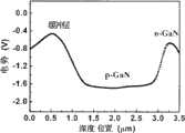
图2为本发明实施例中GaN基p-n结结构剖面生长方向相对导电针尖的表面电势分布。Fig. 2 is the surface potential distribution of the GaN-based p-n junction structure section growth direction relative to the conductive tip in the embodiment of the present invention.
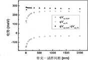
图3为本发明实施例中导电针尖在铂和n-GaN表面测得的相对电势与针尖-试样间距的关系。Fig. 3 is the relationship between the relative potential measured by the conductive needle tip on the surface of platinum and n-GaN and the distance between the needle tip and the sample in the embodiment of the present invention.
图4为本发明实施例中实际测量和数值模拟得出的GaN器件结构p-n结及其临近区域的表面能带分布。Fig. 4 is the surface energy band distribution of the GaN device structure p-n junction and its adjacent regions obtained from actual measurement and numerical simulation in the embodiment of the present invention.
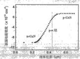
图5为本发明实施例中得出的GaN p-n结附近表面电荷密度分布曲线。Fig. 5 is the surface charge density distribution curve near the GaN p-n junction obtained in the embodiment of the present invention.
图6为本发明实施例中得出的考虑了侧壁表面电荷效应的GaN p-n结二维电场分布。Fig. 6 is a two-dimensional electric field distribution of a GaN p-n junction obtained in an embodiment of the present invention considering the sidewall surface charge effect.
具体实施方式Detailed ways
下面以GaN p-n结结构为实施例,结合附图对本发明的具体实施方式作详细说明:Taking the GaN p-n junction structure as an example below, the specific implementation of the present invention will be described in detail in conjunction with the accompanying drawings:
图1是本发明的测量示意图,该方法适用的探测器结构至少包括一衬底、一p型层和一n型层,其中p型层和n型层可以是GaN或AlGaN材料,其中试样的制备包括公共电极的引出和剖面的制备。公共电极由器件的上表面蒸镀一层金属,经退火后形成欧姆接触而引出;待测剖面由金刚石刀划片自然解理获得。Fig. 1 is the measurement schematic diagram of the present invention, and the applicable detector structure of this method at least comprises a substrate, a p-type layer and an n-type layer, wherein p-type layer and n-type layer can be GaN or AlGaN material, wherein sample The preparation includes the extraction of the common electrode and the preparation of the section. The common electrode is drawn out by evaporating a layer of metal on the upper surface of the device and forming an ohmic contact after annealing; the section to be measured is obtained by natural cleavage by diamond knife scribing.
在本实施例中,所测的器件结构沿材料生长方向依次是蓝宝石衬底层、非故意掺杂GaN缓冲层、p型GaN层以及n型GaN层,其中n型导电层由Si离子注入形成。在n型GaN层的上表面蒸镀Ti/Al,退火后形成欧姆接触,见图1。样品解理后固定在测量基片上,其中解理面垂直向上,公共电极经由基片引出。表面电势的测量采用美国Veeco公司生产的Multimode Nanoscope IV扫描探针显微镜的表面电势成像模式,选用Pt涂层的导电针尖。In this embodiment, the measured device structure along the material growth direction is a sapphire substrate layer, an unintentionally doped GaN buffer layer, a p-type GaN layer and an n-type GaN layer, wherein the n-type conductive layer is formed by Si ion implantation. Evaporate Ti/Al on the upper surface of the n-type GaN layer, and form an ohmic contact after annealing, as shown in Figure 1. After the sample is cleaved, it is fixed on the measurement substrate, wherein the cleavage plane is vertically upward, and the common electrode is drawn out through the substrate. The measurement of the surface potential adopts the surface potential imaging mode of the Multimode Nanoscope IV scanning probe microscope produced by Veeco Company of the United States, and a Pt-coated conductive tip is selected.
根据上述方法由表面电势成像方法测得的剖面-针尖相对电势分布见图2,不同材料和掺杂区域以及它们之间的过渡区域在测量表面的表面电势分布都可以清晰地呈现出来。The cross-section-tip relative potential distribution measured by the surface potential imaging method according to the above method is shown in Figure 2. The surface potential distribution of different materials and doped regions and the transition regions between them can be clearly presented on the measurement surface.
对相对表面电势的定标选用新蒸镀的Pt薄膜作为标准金属试样,图3是导电针尖在Pt薄膜和n型(6×1018cm-3)GaN表面不同距离测得的相对电势,为保证可比对性和降低定标误差,对两种试样的测量采用了相同的导电针尖和参数设置。图3显示,虽然随着针尖-试样间距增加,测得的相对电势也发生变化,但两种试样相对电势之差qVsp,GaN-qVsp,Pt基本维持在275±8meV,体现良好的置信度。再利用关系式Ec=φm-qeVsp,m+qeVsp,dev-χ计算出图2中任一点相对电势对应的表面导带相对费米能级位置,并得到表面能带分布(图4的数据点)。For the calibration of the relative surface potential, a freshly evaporated Pt thin film is used as the standard metal sample. Figure 3 shows the relative potential measured at different distances between the conductive tip of the Pt thin film and the n-type (6×1018 cm-3 ) GaN surface. In order to ensure comparability and reduce calibration errors, the same conductive tip and parameter settings were used for the measurement of the two samples. Figure 3 shows that although the measured relative potential changes as the tip-sample distance increases, the relative potential difference qVsp, GaN -qVsp, and Pt between the two samples are basically maintained at 275±8meV, showing a good performance confidence level. Then use the relationship Ec = φm -qe Vsp, m + qe Vsp, dev - χ to calculate the position of the surface conduction band relative to the Fermi level corresponding to the relative potential of any point in Figure 2, and obtain the surface energy band distribution (data points in Figure 4).
由Sentaurus Device软件建立所测体系的数值模型对获得的表面能带分布进行拟合,其中试样的材料结构、掺杂条件和参数按照实际情况给定;在GaN材料生长方向上分层建模以获得侧壁表面可调的电荷种类和密度分布;单层的厚度在p-n结和n型掺杂浓度递变区域为2到5纳米以反映体内较强的能带变化趋势,而在典型的p型和n型区,由于体内能带平滑,则采用20至100纳米的层厚。由此以各层表面固定电荷种类和密度作为变量,拟合得到和测量值相一致的侧壁表面能带分布(图4);图5给出了相应的p-n结附近的表面固定电荷分布,值得提出的是,表面电荷密度分布对体内相对能带位置的微分即是GaN禁带中的表面电子态密度分布。The numerical model of the measured system is established by Sentaurus Device software to fit the obtained surface energy band distribution, in which the material structure, doping conditions and parameters of the sample are given according to the actual situation; layered modeling in the growth direction of GaN material To obtain adjustable charge species and density distribution on the sidewall surface; the thickness of the single layer is 2 to 5 nanometers in the p-n junction and n-type doping concentration gradient region to reflect the strong energy band change trend in the body, while in the typical For the p-type and n-type regions, layer thicknesses of 20 to 100 nm are used due to the smooth energy bands in the body. Therefore, using the fixed charge species and density on the surface of each layer as variables, the fitted sidewall surface energy band distribution is consistent with the measured value (Fig. 4); Fig. 5 shows the corresponding surface fixed charge distribution near the p-n junction, It is worth mentioning that the differential of the surface charge density distribution to the relative energy band position in the body is the surface electronic density of states distribution in the GaN forbidden band.
从模拟结果中,还可以计算得到器件表面和体内的电场分布等信息(图6),从而有利于预测和分析相似工艺条件下制成的台面型GaN器件单元的性能。From the simulation results, information such as the electric field distribution on the surface and in the body of the device can also be calculated (Figure 6), which is conducive to predicting and analyzing the performance of mesa-type GaN device units fabricated under similar process conditions.
以上所述的实施例仅为了说明本发明的技术思想及特点,其目的在于使本领域的普通技术人员能够了解本发明的内容并据以实施,本发明的范围不仅局限于上述具体实施例,即凡依本发明所揭示的精神所作的同等变化或修饰,仍涵盖在本发明的保护范围。The above-described embodiments are only to illustrate the technical ideas and characteristics of the present invention, and its purpose is to enable those of ordinary skill in the art to understand the content of the present invention and implement it accordingly. The scope of the present invention is not limited to the above-mentioned specific embodiments. That is, all equivalent changes or modifications made according to the spirit disclosed in the present invention still fall within the protection scope of the present invention.
Claims (5)
Priority Applications (1)
| Application Number | Priority Date | Filing Date | Title |
|---|---|---|---|
| CN 201010101896CN101769941B (en) | 2010-01-27 | 2010-01-27 | Electronic detection method of device structure of GaN base photovoltaic detector |
Applications Claiming Priority (1)
| Application Number | Priority Date | Filing Date | Title |
|---|---|---|---|
| CN 201010101896CN101769941B (en) | 2010-01-27 | 2010-01-27 | Electronic detection method of device structure of GaN base photovoltaic detector |
Publications (2)
| Publication Number | Publication Date |
|---|---|
| CN101769941Atrue CN101769941A (en) | 2010-07-07 |
| CN101769941B CN101769941B (en) | 2013-04-17 |
Family
ID=42502929
Family Applications (1)
| Application Number | Title | Priority Date | Filing Date |
|---|---|---|---|
| CN 201010101896Expired - Fee RelatedCN101769941B (en) | 2010-01-27 | 2010-01-27 | Electronic detection method of device structure of GaN base photovoltaic detector |
Country Status (1)
| Country | Link |
|---|---|
| CN (1) | CN101769941B (en) |
Cited By (3)
| Publication number | Priority date | Publication date | Assignee | Title |
|---|---|---|---|---|
| CN107402184A (en)* | 2016-05-20 | 2017-11-28 | 清华大学 | A kind of method for measuring nanostructured surface distribution of charges |
| CN108646160A (en)* | 2018-04-10 | 2018-10-12 | 中国科学院上海技术物理研究所 | The measuring device and method of minority carrier Subspace Distribution in low-gap semiconductor |
| CN116298400A (en)* | 2023-03-09 | 2023-06-23 | 南昌大学 | A characterization method for detecting the activation effect of p-type group III nitrides |
Citations (5)
| Publication number | Priority date | Publication date | Assignee | Title |
|---|---|---|---|---|
| JP2002064201A (en)* | 2000-08-18 | 2002-02-28 | Toshiba Corp | Semiconductor field effect transistor and power amplifier |
| CN1681134A (en)* | 2004-04-07 | 2005-10-12 | 中国科学院半导体研究所 | Gallium Nitride-based Schottky Structure Ultraviolet Detector and Manufacturing Method |
| US20050285155A1 (en)* | 2004-06-28 | 2005-12-29 | Nitronex Corporation | Semiconductor device-based sensors and methods associated with the same |
| CN101127368A (en)* | 2001-07-23 | 2008-02-20 | 美商克立股份有限公司 | GaN Substrate Diodes with Low Forward Voltage and Low Reverse Current Operation |
| CN101494244A (en)* | 2009-03-04 | 2009-07-29 | 中国科学院上海技术物理研究所 | Back irradiation plane type PIN structure GaN-based ultraviolet detector and preparation method |
- 2010
- 2010-01-27CNCN 201010101896patent/CN101769941B/ennot_activeExpired - Fee Related
Patent Citations (5)
| Publication number | Priority date | Publication date | Assignee | Title |
|---|---|---|---|---|
| JP2002064201A (en)* | 2000-08-18 | 2002-02-28 | Toshiba Corp | Semiconductor field effect transistor and power amplifier |
| CN101127368A (en)* | 2001-07-23 | 2008-02-20 | 美商克立股份有限公司 | GaN Substrate Diodes with Low Forward Voltage and Low Reverse Current Operation |
| CN1681134A (en)* | 2004-04-07 | 2005-10-12 | 中国科学院半导体研究所 | Gallium Nitride-based Schottky Structure Ultraviolet Detector and Manufacturing Method |
| US20050285155A1 (en)* | 2004-06-28 | 2005-12-29 | Nitronex Corporation | Semiconductor device-based sensors and methods associated with the same |
| CN101494244A (en)* | 2009-03-04 | 2009-07-29 | 中国科学院上海技术物理研究所 | Back irradiation plane type PIN structure GaN-based ultraviolet detector and preparation method |
Non-Patent Citations (2)
| Title |
|---|
| 刘云燕等: "GaN基紫外光探测器的研究进展", 《半导体技术》* |
| 李向阳等: "GaN基紫外探测器及其研究进展", 《红外与激光工程》* |
Cited By (5)
| Publication number | Priority date | Publication date | Assignee | Title |
|---|---|---|---|---|
| CN107402184A (en)* | 2016-05-20 | 2017-11-28 | 清华大学 | A kind of method for measuring nanostructured surface distribution of charges |
| CN107402184B (en)* | 2016-05-20 | 2020-01-03 | 清华大学 | Method for measuring surface charge distribution of nano structure |
| CN108646160A (en)* | 2018-04-10 | 2018-10-12 | 中国科学院上海技术物理研究所 | The measuring device and method of minority carrier Subspace Distribution in low-gap semiconductor |
| CN108646160B (en)* | 2018-04-10 | 2023-07-04 | 中国科学院上海技术物理研究所 | Apparatus and method for measuring the spatial distribution of minority carriers in narrow bandgap semiconductors |
| CN116298400A (en)* | 2023-03-09 | 2023-06-23 | 南昌大学 | A characterization method for detecting the activation effect of p-type group III nitrides |
Also Published As
| Publication number | Publication date |
|---|---|
| CN101769941B (en) | 2013-04-17 |
Similar Documents
| Publication | Publication Date | Title |
|---|---|---|
| Oliver | Advances in AFM for the electrical characterization of semiconductors | |
| Maragliano et al. | Quantifying charge carrier concentration in ZnO thin films by Scanning Kelvin Probe Microscopy | |
| Tennyson et al. | Imaging energy harvesting and storage systems at the nanoscale | |
| CN102621465B (en) | Method for detecting minority carrier lifetime of semiconductor nanowire | |
| CN102175727B (en) | Method for measuring low background carrier concentration by utilizing optical excitation differential capacitance method | |
| Chen et al. | Insight into interfaces and junction of polycrystalline silicon solar cells by kelvin probe force microscopy | |
| CN101865871A (en) | A Method for Measuring the Mobility of Organic Thin Films Based on Schottky Contact IV Analysis | |
| Abou-Ras et al. | Electron-beam-induced current measurements of thin-film solar cells | |
| CN101769941B (en) | Electronic detection method of device structure of GaN base photovoltaic detector | |
| Leite et al. | Mapping the local photoelectronic properties of polycrystalline solar cells through high resolution laser-beam-induced current microscopy | |
| CN102830260B (en) | Method for measuring carrier concentration in semiconductor quantum well | |
| Jiang et al. | The nanometer-resolution local electrical potential and resistance mapping of CdTe thin films | |
| Geng et al. | Three-Dimensional Kelvin Probe Force Microscopy | |
| Hu et al. | Investigating size-dependent conductive properties on individual Si nanowires | |
| Xiao et al. | Locating the electrical junctions in Cu (In, Ga) Se2 and Cu2ZnSnSe4 solar cells by scanning capacitance spectroscopy | |
| Teferi et al. | Imaging of bandtail states in silicon heterojunction solar cells: Nanoscopic current effects on photovoltaics | |
| CN102544185A (en) | Light spot position detection sensor | |
| Wu et al. | Electrical anisotropy properties of ZnO nanorods analyzed by conductive atomic force microscopy | |
| CN105047814B (en) | A kind of silicon substrate downfield giant magnetoresistance magnetic sensor device and preparation and performance test methods | |
| Ye et al. | Direct observation of surface charge redistribution in active nanoscale conducting channels by Kelvin Probe Force Microscopy | |
| CN107907713B (en) | A kind of detection method and application of electrical properties of single soot nanoparticles | |
| Ishida | Local impedance measurement by direct detection of oscillating electrostatic potential using kelvin probe force microscopy | |
| Gicevičius et al. | Probing Out‐Of‐Plane Charge Transport in Organic Semiconductors Using Conductive Atomic Force Microscopy | |
| Jiang et al. | Local Resistance Measurement for Degradation of c-Si Heterojunction with Intrinsic Thin Layer (HIT) Solar Modules | |
| CN103904000B (en) | The method using electric capacity contrast test structure detection polysilicon bottom bridging defect |
Legal Events
| Date | Code | Title | Description |
|---|---|---|---|
| C06 | Publication | ||
| PB01 | Publication | ||
| C10 | Entry into substantive examination | ||
| SE01 | Entry into force of request for substantive examination | ||
| C14 | Grant of patent or utility model | ||
| GR01 | Patent grant | ||
| CF01 | Termination of patent right due to non-payment of annual fee | Granted publication date:20130417 Termination date:20220127 | |
| CF01 | Termination of patent right due to non-payment of annual fee |