CN101764054B - Compound semiconductor epitaxial chip and manufacturing method thereof - Google Patents
Compound semiconductor epitaxial chip and manufacturing method thereofDownload PDFInfo
- Publication number
- CN101764054B CN101764054BCN200810187928XACN200810187928ACN101764054BCN 101764054 BCN101764054 BCN 101764054BCN 200810187928X ACN200810187928X ACN 200810187928XACN 200810187928 ACN200810187928 ACN 200810187928ACN 101764054 BCN101764054 BCN 101764054B
- Authority
- CN
- China
- Prior art keywords
- compound semiconductor
- epitaxial
- buffer layer
- layer
- manufacturing
- Prior art date
- Legal status (The legal status is an assumption and is not a legal conclusion. Google has not performed a legal analysis and makes no representation as to the accuracy of the status listed.)
- Expired - Fee Related
Links
- 150000001875compoundsChemical class0.000titleclaimsabstractdescription273
- 239000004065semiconductorSubstances0.000titleclaimsabstractdescription272
- 238000004519manufacturing processMethods0.000titleclaimsabstractdescription93
- 238000000034methodMethods0.000claimsabstractdescription91
- 238000010438heat treatmentMethods0.000claimsabstractdescription61
- 229910052710siliconInorganic materials0.000claimsabstractdescription55
- 239000010703siliconSubstances0.000claimsabstractdescription55
- 239000000758substrateSubstances0.000claimsabstractdescription46
- 238000000151depositionMethods0.000claimsabstractdescription26
- 229910052751metalInorganic materials0.000claimsabstractdescription24
- 239000002184metalSubstances0.000claimsabstractdescription24
- JBRZTFJDHDCESZ-UHFFFAOYSA-NAsGaChemical compound[As]#[Ga]JBRZTFJDHDCESZ-UHFFFAOYSA-N0.000claimsdescription67
- 229910001218Gallium arsenideInorganic materials0.000claimsdescription62
- XUIMIQQOPSSXEZ-UHFFFAOYSA-NSiliconChemical compound[Si]XUIMIQQOPSSXEZ-UHFFFAOYSA-N0.000claimsdescription53
- 238000000137annealingMethods0.000claimsdescription29
- 230000008569processEffects0.000claimsdescription27
- 238000005137deposition processMethods0.000claimsdescription23
- 239000000463materialSubstances0.000claimsdescription22
- 239000010409thin filmSubstances0.000claimsdescription22
- 230000008021depositionEffects0.000claimsdescription19
- 125000004122cyclic groupChemical group0.000claimsdescription12
- 238000005229chemical vapour depositionMethods0.000claimsdescription10
- 238000000407epitaxyMethods0.000claimsdescription8
- GPXJNWSHGFTCBW-UHFFFAOYSA-NIndium phosphideChemical compound[In]#PGPXJNWSHGFTCBW-UHFFFAOYSA-N0.000claimsdescription6
- HZXMRANICFIONG-UHFFFAOYSA-Ngallium phosphideChemical compound[Ga]#PHZXMRANICFIONG-UHFFFAOYSA-N0.000claimsdescription6
- RPQDHPTXJYYUPQ-UHFFFAOYSA-Nindium arsenideChemical compound[In]#[As]RPQDHPTXJYYUPQ-UHFFFAOYSA-N0.000claimsdescription5
- 238000001451molecular beam epitaxyMethods0.000claimsdescription5
- 229910005540GaPInorganic materials0.000claimsdescription4
- 229910000673Indium arsenideInorganic materials0.000claimsdescription4
- MDPILPRLPQYEEN-UHFFFAOYSA-Naluminium arsenideChemical compound[As]#[Al]MDPILPRLPQYEEN-UHFFFAOYSA-N0.000claimsdescription4
- 239000013078crystalSubstances0.000abstractdescription20
- 239000010408filmSubstances0.000description8
- 238000005259measurementMethods0.000description6
- RBFQJDQYXXHULB-UHFFFAOYSA-NarsaneChemical compound[AsH3]RBFQJDQYXXHULB-UHFFFAOYSA-N0.000description5
- 230000000694effectsEffects0.000description5
- 238000005516engineering processMethods0.000description4
- XCZXGTMEAKBVPV-UHFFFAOYSA-NtrimethylgalliumChemical compoundC[Ga](C)CXCZXGTMEAKBVPV-UHFFFAOYSA-N0.000description4
- 229910000530Gallium indium arsenideInorganic materials0.000description3
- 238000004891communicationMethods0.000description3
- 238000010586diagramMethods0.000description3
- 239000007789gasSubstances0.000description3
- 230000006872improvementEffects0.000description3
- 238000012986modificationMethods0.000description3
- 230000004048modificationEffects0.000description3
- 230000005693optoelectronicsEffects0.000description3
- BLRPTPMANUNPDV-UHFFFAOYSA-NSilaneChemical compound[SiH4]BLRPTPMANUNPDV-UHFFFAOYSA-N0.000description2
- 230000009286beneficial effectEffects0.000description2
- 230000007547defectEffects0.000description2
- 238000013461designMethods0.000description2
- 230000017525heat dissipationEffects0.000description2
- 238000002360preparation methodMethods0.000description2
- 239000012495reaction gasSubstances0.000description2
- 229910052782aluminiumInorganic materials0.000description1
- XAGFODPZIPBFFR-UHFFFAOYSA-NaluminiumChemical compound[Al]XAGFODPZIPBFFR-UHFFFAOYSA-N0.000description1
- 229910021417amorphous siliconInorganic materials0.000description1
- 238000011161developmentMethods0.000description1
- 229910052732germaniumInorganic materials0.000description1
- GNPVGFCGXDBREM-UHFFFAOYSA-Ngermanium atomChemical compound[Ge]GNPVGFCGXDBREM-UHFFFAOYSA-N0.000description1
- -1howeverChemical compound0.000description1
- 229910021421monocrystalline siliconInorganic materials0.000description1
- 230000003287optical effectEffects0.000description1
- 230000035515penetrationEffects0.000description1
- 230000008092positive effectEffects0.000description1
- 230000000750progressive effectEffects0.000description1
- 230000009467reductionEffects0.000description1
- 238000012827research and developmentMethods0.000description1
- 229910000077silaneInorganic materials0.000description1
- 239000000126substanceSubstances0.000description1
- 238000007740vapor depositionMethods0.000description1
Images


Landscapes
- Recrystallisation Techniques (AREA)
- Chemical Vapour Deposition (AREA)
Abstract
Description
Translated fromChinese技术领域technical field
本发明涉及一种化合物半导体及其制造方法,特别是涉及一种长于一金属基板上的化合物半导体外延芯片及其制造方法。The invention relates to a compound semiconductor and its manufacturing method, in particular to a compound semiconductor epitaxial chip longer than a metal substrate and its manufacturing method.
背景技术Background technique
随着光电及通讯产业急速发展,化合物半导体如砷化镓(GaAs)等III-V族化合物凭借其直接能隙(direct band-gap)、高载子迁移率(carrier mobility)、以及藉由调整III-V族化合物的化学组成可得到不同能隙的材料…等优越特性已成为制作光电及通讯组件的主要基材。With the rapid development of the optoelectronic and communication industries, compound semiconductors such as gallium arsenide (GaAs) and other III-V compounds rely on their direct band-gap, high carrier mobility, and by adjusting The chemical composition of III-V compounds can obtain materials with different energy gaps... and other superior properties have become the main substrates for making optoelectronic and communication components.
III-V族化合物半导体的光电及通讯组件的制作主要是以砷化镓(GaAs)、磷化镓(GaP)及磷化铟(InP)等III-V族化合物为基板(substrate),在晶格(lattice)匹配的状况下进行外延成长。目前,III-V族化合物半导体基板的直径多为四英时以下的砷化镓(GaAs)或锗(Ge)材料基板,或使用单晶硅基板(Si)。The optoelectronic and communication components of III-V compound semiconductors are mainly made of III-V compounds such as gallium arsenide (GaAs), gallium phosphide (GaP) and indium phosphide (InP) as substrates. The epitaxial growth is carried out under the condition of lattice (lattice) matching. At present, most of the III-V compound semiconductor substrates are gallium arsenide (GaAs) or germanium (Ge) material substrates with a diameter of less than four inches, or single crystal silicon substrates (Si).
然而,由于缓冲层与III-V族化合物半导体材料之间存在晶格不匹配及热膨胀系数(thermal expansion coefficient)不同等问题,例如,硅缓冲层与砷化镓材料的晶格常数在25℃时相差约为4.1%,再者,硅缓冲层与砷化镓材料的热膨胀系数在25℃时相差约为62%。因此,将III-V化合物半导体材料外延于缓冲层上,会因为晶格不匹配及热膨胀系数不同等问题,在化合物半导体外延层内形成贯穿式位错(threadingdlslocation),从而造成结晶质量不佳。However, due to the problems of lattice mismatch and thermal expansion coefficient between the buffer layer and the III-V compound semiconductor material, for example, the lattice constant of the silicon buffer layer and the gallium arsenide material is different at 25° C. The difference is about 4.1%. Moreover, the difference in thermal expansion coefficient between the silicon buffer layer and GaAs material is about 62% at 25°C. Therefore, epitaxial III-V compound semiconductor materials on the buffer layer will form threading dislocations (threadingdlslocation) in the compound semiconductor epitaxial layer due to problems such as lattice mismatch and thermal expansion coefficient, resulting in poor crystal quality.
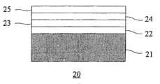
请参阅图1所示,为第一现有习知的技术在硅基板上成长化合物半导体外延的剖面示意图。一化合物半导体外延芯片20包含:一硅基板21、一砷化镓第一缓冲层22、一砷化镓第一外延层23、一砷化镓第二缓冲层24、一砷化镓第二外延层25。该化合物半导体外延芯片20的制备方法是采用有机金属化学气相沉积(metal-organic chemical vapor deposition)法,首先对该硅基板21进行一沉积制造工艺,其中该沉积制造工艺的温度约为450℃,沉积后形成该砷化镓第一缓冲层22的厚度为5至20μm。接着进行该砷化镓第一外延层的外延制造工艺,其中外延制造工艺的温度为650℃,外延后形成该砷化镓第一外延层23的厚度为1μm。接着再进行一沉积制造工艺,其中该沉积制造工艺的温度亦约为450℃,沉积后形成该砷化镓第二缓冲层24的厚度为5至20nm。接续再进行该砷化镓第二外延层的外延制造工艺,其中外延制造工艺的温度亦约为650℃,外延后形成该砷化嫁第二外延层25的厚度约为2μm。Please refer to FIG. 1 , which is a schematic cross-sectional view of growing compound semiconductor epitaxy on a silicon substrate in the first prior art. A compound semiconductor
前述第一现有习知的技术是利用二层砷化镓缓冲层(22、24)及二层砷化镓外延层(23,25)来改善砷化镓在硅基板21上外延的品质。但此一制造工艺仍需再加入一温度循环退火(thermal cycle annealing)的热处理程序才可进一步有效改善砷化镓外延层的质量。The aforementioned first prior art technology is to improve the quality of GaAs epitaxy on the
请参阅图2所示,为第二现有习知的技术的化合物半导体外延芯片剖面示意图。一化合物半导体外延芯片30包含:一硅基板31、一砷化镓第一缓冲层32、一砷化镓第一外延层33、一砷化镓第二缓冲层34、一砷化镓第二外延层35。该化合物半导体外延芯片30的制备方法亦是采用有机金属化学气相沉积法,首先对该硅基板31进行一沉积制造工艺,其中沉积制造工艺的温度为430℃,沉积后形成该砷化镓第一缓冲层32的厚度为50nm。接着进行该砷化镓第一外延层33的外延制造工艺,其中外延制造工艺的温度为620℃,外延后形成该砷化镓第一外延层33的厚度为2μm。此时,紧接着进行温度循环退火热处理程序,首先将有机金属化学气相沉积系统内的外延芯片温度降至300℃,到达此一温度后,再加热外延芯片至750℃,并在750℃维特5分钟,然后再降低温度至300℃,如此是一个温度循环。当经过一个或四个温度循环退火热处理后接着再进行一沉积制造工艺,其中该沉积制造工艺的温度为620℃,沉积后形成该砷化铟镓第二缓冲层34的厚度为200nm。接着再进行该砷化镓第二外延层35的外延制造工艺,其中外延制造工艺的温度亦为620℃,外延后形成该砷化镓第二外延层35的厚度为1.8μm。Please refer to FIG. 2 , which is a schematic cross-sectional view of a compound semiconductor epitaxial chip in the second prior art. A compound semiconductor
此第二现有习知的技术是利用一层砷化镓第一缓冲层32及一层砷化镓第一外延层33,经过温度循环退火热处理来降低贯穿式位错产生的机会,进而成长该砷化铟镓第二缓冲层34、该砷化录第二外延层35,以改善砷化镓在该硅基板31上的外延品质。依据第二现有习知的技术的结果显示,在经过一次温度循环退火热处理状况下,该砷化镓第一外延层33的双晶X射线摇摆曲线(double crystal X-ray rocking curve)量测呈现半高波宽(FullWidth at Half Maximum,FWHM)值为280arcsec。然而,在经过四次温度循环退火热处理状况下,该砷化镓第一外延层33的双晶X-射线摇摆曲线量测呈现半高波宽值降为140arcsec。此一现象表示温度循环退火热处理对于砷化镓在硅基板的外延质量有显著的效用。This second conventional technology is to use a layer of GaAs
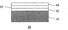
请参阅图3所示,为第三现有习知的技术的化合物半导体外延芯片剖面示意图。一化合物半导体外延芯片40包含:一硅基板41、一砷化镓第一缓冲层42、一砷化镓第一外延层43、一砷化镓第二外延层44。该化合物半导体外延芯片40的制备方法亦是采用有机金属化学气相沉积法,首先对该硅基板41进行一沉积制造工艺,其中沉积制造工艺的温度为400℃,沉积后形成该砷化镓第一缓冲层42的厚度小于200nm。接着进行该砷化镓第一外延层43的外延制造工艺,其中外延制造工艺的温度为700℃,外延后形成该砷化镓第一外延层43的厚度为1μm。此时,紧接着进行温度循环退火热处理程序,首先将有机金属化学气相沉积系统内的外延芯片温度降至室温,到达此一温度后,再加热外延至850℃,并在850℃维持5分钟,然后再降低温度至700℃。接着,进行该砷化镓第二外延层44的外延成长,如此是一个温度循环外延程序,当经过三个至十三个温度循环外延程序后,同时完成热处理及该砷化镓第二外延层44的外延成长制造工艺,形成该砷化镓第二外延层44的厚度为3~4μm。Please refer to FIG. 3 , which is a schematic cross-sectional view of a compound semiconductor epitaxial chip in the third prior art. A compound semiconductor
此第三现有习知的技术是利用一层砷化镓第一缓冲层42、一层砷化镓第一外延层43及同时进行温度循环退火热处理与外延制造工艺的方式来降低贯穿式位错的产生,进而得到该砷化镓第二外延层44,以改善砷化镓在硅基板41上的外延品质。依据伊藤(Itoh)等人的实验结果显示,在经过三个至十三个温度循环外延程序后,该砷化镓第二外延层44的双晶X-射线摇摆曲线量测呈现半高波宽值为130arcsec。因此,第三现有习知的技术所采用的方法虽然可改进砷化镓的外延质量,但是由双晶X-射线摇摆曲线量测结果来看,该砷化镓第二外延层44的质量仍是相当低落。This third prior known technology is to reduce the penetration potential by using a
因此,在化合物半导体外延芯片中,制造工艺步骤、外延结构以及温度循环退火热处理程序皆攸关着外延芯片的晶体质量。Therefore, in the compound semiconductor epitaxial chip, the manufacturing process steps, the epitaxial structure and the temperature cycle annealing heat treatment procedure are all related to the crystal quality of the epitaxial chip.
由此可见,上述现有的化合物半导体外延芯片及其制造方法在产品结构、制造方法与使用上,显然仍存在有不便与缺陷,而亟待加以进一步改进。为了解决上述存在的问题,相关厂商莫不费尽心思来谋求解决之道,但长久以来一直未见适用的设计被发展完成,而一般产品及方法又没有适切的结构及方法能够解决上述问题,此显然是相关业者急欲解决的问题。因此如何能创设一种新的化合物半导体外延芯片及其制造方法,实属当前重要研发课题之一,亦成为当前业界极需改进的目标。It can be seen that the above-mentioned existing compound semiconductor epitaxial chip and its manufacturing method obviously still have inconveniences and defects in terms of product structure, manufacturing method and use, and need to be further improved. In order to solve the above-mentioned problems, the relevant manufacturers have tried their best to find a solution, but no suitable design has been developed for a long time, and there is no suitable structure and method for general products and methods to solve the above-mentioned problems. This is obviously a problem that relevant industry players are eager to solve. Therefore, how to create a new compound semiconductor epitaxial chip and its manufacturing method is one of the current important research and development topics, and it has also become a goal that the industry needs to improve.
发明内容Contents of the invention
本发明的目的在于,克服现有的化合物半导体外延芯片及其制造方法存在的缺陷,而提供一种具有良好晶体质量及特性的化合物半导体外延芯片及其制造方法,所要解决的技术问题是使其利用金属基板的基材改良,与外延结构及温度循环退火热处理程序的制造工艺步骤改进,来达到晶体质量增进、制造工艺简化与成本降低的优点,非常适于实用。The object of the present invention is to overcome the defects of existing compound semiconductor epitaxial chip and its manufacturing method, and provide a compound semiconductor epitaxial chip with good crystal quality and characteristics and its manufacturing method. The technical problem to be solved is to make it The improvement of the base material of the metal substrate, the improvement of the manufacturing process steps of the epitaxial structure and the temperature cycle annealing heat treatment procedure are used to achieve the advantages of crystal quality improvement, manufacturing process simplification and cost reduction, which is very suitable for practical use.
本发明的目的及解决其技术问题是采用以下技术方案来实现的。依据本发明提出的一种化合物半导体外延芯片的制造方法,其包含以下步骤:在一金属基板上沉积一层硅薄膜以形成一硅第一缓冲层;在该硅第一缓冲层上沉积一层化合物半导体薄膜以形成一化合物半导体第二缓冲层;在该化合物半导体第二缓冲层上沉积一层化合物半导体薄膜以形成一化合物半导体第三缓冲层;在该化合物半导体第三缓冲层上外延一层化合物半导体薄膜以形成一化合物半导体第一外延层;施以一第一次热处理程序;在该化合物半导体第一外延层上外延一层化合物半导体薄膜以形成一化合物半导体第二外延层;以及施以一第二次热处理程序以完成一化合物半导体外延芯片。The purpose of the present invention and the solution to its technical problems are achieved by adopting the following technical solutions. A method for manufacturing a compound semiconductor epitaxial chip according to the present invention comprises the following steps: depositing a silicon film on a metal substrate to form a silicon first buffer layer; depositing a silicon first buffer layer on the silicon first buffer layer Compound semiconductor thin film to form a compound semiconductor second buffer layer; Deposit a layer of compound semiconductor thin film on the compound semiconductor second buffer layer to form a compound semiconductor third buffer layer; Epitaxially layer a compound semiconductor on the compound semiconductor third buffer layer compound semiconductor thin film to form a compound semiconductor first epitaxial layer; apply a first heat treatment process; epitaxially layer a compound semiconductor thin film on the compound semiconductor first epitaxial layer to form a compound semiconductor second epitaxial layer; and apply A second heat treatment process to complete a compound semiconductor epitaxial chip.
本发明的目的及解决其技术问题还可采用以下技术措施进一步实现。The purpose of the present invention and its technical problems can also be further realized by adopting the following technical measures.
前述的化合物半导体外延芯片的制造方法,其中所述的化合物半导体薄膜为砷化镓、砷化铝、磷化镓、砷化铟、磷化铟等III-V族化合物半导体二元材料或由其组成的三元或四元材料。The method for manufacturing the aforementioned compound semiconductor epitaxial chip, wherein the compound semiconductor thin film is a III-V compound semiconductor binary material such as gallium arsenide, aluminum arsenide, gallium phosphide, indium arsenide, indium phosphide, or a combination thereof Composed of ternary or quaternary materials.
前述的化合物半导体外延芯片的制造方法,其中沉积的制造工艺为一有机金属化学气相沉积制造工艺。In the aforementioned method for manufacturing a compound semiconductor epitaxial chip, the deposition process is a metal-organic chemical vapor deposition process.
前述的化合物半导体外延芯片的制造方法,其中外延的制造工艺为一分子束外延制造工艺。In the aforementioned method for manufacturing a compound semiconductor epitaxial chip, the epitaxial manufacturing process is a molecular beam epitaxy manufacturing process.
前述的化合物半导体外延芯片的制造方法,其中所述的硅第一缓冲层的沉积制造工艺在温度为580~600℃下进行。The aforementioned method for manufacturing a compound semiconductor epitaxial chip, wherein the deposition and manufacturing process of the silicon first buffer layer is carried out at a temperature of 580-600°C.
前述的化合物半导体外延芯片的制造方法,其中所述的硅第一缓冲层的厚度为
前述的化合物半导体外延芯片的制造方法,其中所述的化合物半导体第二缓冲层的沉积制造工艺在温度为380~400℃下进行。The aforementioned method for manufacturing a compound semiconductor epitaxial chip, wherein the deposition and manufacturing process of the compound semiconductor second buffer layer is carried out at a temperature of 380-400°C.
前述的化合物半导体外延芯片的制造方法,其中所述的化合物半导体第二缓冲层的厚度为10至20μm。In the aforementioned method for manufacturing a compound semiconductor epitaxial chip, the thickness of the compound semiconductor second buffer layer is 10 to 20 μm.
前述的化合物半导体外延芯片的制造方法,其中所述的化合物半导体第三缓冲层的沉积制造工艺在温度为400~450℃下进行。The aforementioned method for manufacturing a compound semiconductor epitaxial chip, wherein the deposition and manufacturing process of the third buffer layer of the compound semiconductor is carried out at a temperature of 400-450°C.
前述的化合物半导体外延芯片的制造方法,其中所述的化合物半导体第三缓冲层的厚度为
前述的化合物半导体外延芯片的制造方法,其中所述的化合物半导体第一外延层的外延制造工艺在温度为650℃下进行。The aforementioned method for manufacturing a compound semiconductor epitaxial chip, wherein the epitaxial manufacturing process of the first epitaxial layer of the compound semiconductor is carried out at a temperature of 650°C.
前述的化合物半导体外延芯片的制造方法,其中所述的化合物半导体第二外延层的外延制造工艺在温度为710℃下进行。In the aforementioned method for manufacturing a compound semiconductor epitaxial chip, the epitaxial manufacturing process of the second epitaxial layer of the compound semiconductor is carried out at a temperature of 710°C.
前述的化合物半导体外延芯片的制造方法,其中所述的化合物半导体第一外延层的厚度为1.5~2μm。The aforementioned method for manufacturing a compound semiconductor epitaxial chip, wherein the thickness of the first compound semiconductor epitaxial layer is 1.5-2 μm.
前述的化合物半导体外延芯片的制造方法,其中所述的化合物半导体第二外延层的厚度为1.5~2μm。The aforementioned method for manufacturing a compound semiconductor epitaxial chip, wherein the thickness of the second compound semiconductor epitaxial layer is 1.5-2 μm.
前述的化合物半导体外延芯片的制造方法,其中该第一次热处理程序与该第二次热处理程序皆为一高低温循环退火热处理程序,该高低温循环退火热处理程序经过4~8次的高低温循环。The aforementioned method for manufacturing a compound semiconductor epitaxial chip, wherein the first heat treatment procedure and the second heat treatment procedure are both a high-low temperature cyclic annealing heat treatment procedure, and the high-low temperature cyclic annealing heat treatment procedure undergoes 4 to 8 high-low temperature cycles .
本发明的目的及解决其技术问题还采用以下技术方案来实现。依据本发明提出的一种化合物半导体外延芯片,其包含:一金属基板;一硅第一缓冲层,设置于该金属基板上;一化合物半导体第二缓冲层,设置于该硅第一缓冲层上;一化合物半导体第三缓冲层,设置于该化合物半导体第二缓冲层上,该化合物半导体第三缓冲层并经过一第一次热处理程序;一化合物半导体第一外延层,设置于该化合物半导体第三缓冲层上;及一化合物半导体第二外延层,设置于该化合物半导体第一外延层上,该化合物半导体第二外延层并经过一第二次热处理程序。The purpose of the present invention and the solution to its technical problem also adopt the following technical solutions to achieve. A compound semiconductor epitaxial chip according to the present invention comprises: a metal substrate; a silicon first buffer layer disposed on the metal substrate; a compound semiconductor second buffer layer disposed on the silicon first buffer layer ; a compound semiconductor third buffer layer, arranged on the compound semiconductor second buffer layer, and the compound semiconductor third buffer layer has undergone a first heat treatment procedure; a compound semiconductor first epitaxial layer, arranged on the compound semiconductor second buffer layer on three buffer layers; and a second compound semiconductor epitaxial layer disposed on the compound semiconductor first epitaxial layer, and the compound semiconductor second epitaxial layer undergoes a second heat treatment procedure.
本发明的目的及解决其技术问题还可采用以下技术措施进一步实现。The purpose of the present invention and its technical problems can also be further realized by adopting the following technical measures.
前述的化合物半导体外延芯片,其中所述的化合物半导体第二缓冲层、该化合物半导体第三缓冲层、该化合物半导体第一外延层及该化合物半导体第二外延层的材料为砷化镓、砷化铝、磷化镓、砷化铟、磷化铟等III-V族化合物半导体二元材料或由其组成的三元或四元材料。The aforementioned compound semiconductor epitaxial chip, wherein the materials of the compound semiconductor second buffer layer, the compound semiconductor third buffer layer, the compound semiconductor first epitaxial layer and the compound semiconductor second epitaxial layer are gallium arsenide, arsenide Aluminum, gallium phosphide, indium arsenide, indium phosphide and other III-V compound semiconductor binary materials or ternary or quaternary materials composed of them.
前述的化合物半导体外延芯片,其中所述的硅第一缓冲层的厚度为
前述的化合物半导体外延芯片,其中所述的化合物半导体第二缓冲层的厚度为10至20μm。The aforementioned compound semiconductor epitaxial chip, wherein the thickness of the compound semiconductor second buffer layer is 10 to 20 μm.
前述的化合物半导体外延芯片,其中所述的化合物半导体第三缓冲层的厚度为
前述的化合物半导体外延芯片,其中所述的化合物半导体第一外延层的厚度为1.5~2μm。The aforementioned compound semiconductor epitaxial chip, wherein the thickness of the first compound semiconductor epitaxial layer is 1.5-2 μm.
前述的化合物半导体外延芯片,其中所述的化合物半导体第一外延层的厚度为1.5~2μm。The aforementioned compound semiconductor epitaxial chip, wherein the thickness of the first compound semiconductor epitaxial layer is 1.5-2 μm.
前述的化合物半导体外延芯片,其中该第一次热处理程序与该第二次热处理程序皆为一高低温循环退火热处理程序,该高低温循环退火热处理程序经过4~8次的高低温循环。In the aforementioned compound semiconductor epitaxial chip, the first heat treatment process and the second heat treatment process are both a high-low temperature cyclic annealing heat treatment process, and the high-low temperature cyclic annealing heat treatment process undergoes 4 to 8 high-low temperature cycles.
本发明与现有技术相比具有明显的优点和有益效果。由以上技术方案可知,本发明的主要技术内容如下:Compared with the prior art, the present invention has obvious advantages and beneficial effects. As can be seen from above technical scheme, main technical content of the present invention is as follows:
为了达到上述目的,本发明提供了一种化合物半导体外延芯片及其制造方法,为达上述目的,本发明的化合物半导体外延芯片的制造方法包含以下步骤:在一金属基板上沉积一层硅薄膜以形成一硅第一缓冲层;在该硅第一缓冲层上沉积一层化合物半导体薄膜以形成一化合物半导体第二缓冲层;在该化合物半导体第二缓冲层上沉积一层化合物半导体薄膜以形成一化合物半导体第三缓冲层;在该化合物半导体第三缓冲层上外延一层化合物半导体薄膜以形成一化合物半导体第一外延层;施以一第一次热处理程序;在该化合物半导体第一外延层上外延一层化合物半导体薄膜以形成一化合物半导体第二外延层;及施以一第二次热处理程序以完成一化合物半导体外延芯片。In order to achieve the above object, the present invention provides a compound semiconductor epitaxial chip and a manufacturing method thereof. To achieve the above object, the manufacturing method of the compound semiconductor epitaxial chip of the present invention includes the following steps: depositing a layer of silicon thin film on a metal substrate to forming a silicon first buffer layer; depositing a compound semiconductor thin film on the silicon first buffer layer to form a compound semiconductor second buffer layer; depositing a compound semiconductor thin film on the compound semiconductor second buffer layer to form a Compound semiconductor third buffer layer; epitaxy a layer of compound semiconductor thin film on the compound semiconductor third buffer layer to form a compound semiconductor first epitaxial layer; apply a first heat treatment procedure; on the compound semiconductor first epitaxial layer epitaxial compound semiconductor thin film to form a compound semiconductor second epitaxial layer; and applying a second heat treatment process to complete a compound semiconductor epitaxial chip.
另外,为了达到上述目的,本发明还提供了一种化合物半导体外延芯片及其制造方法,为达上述目的,本发明的化合物半导体外延芯片包含:一金属基板;一硅第一缓冲层,设置于该金属基板上;一化合物半导体第二缓冲层,设置于该硅第一缓冲层上;一化合物半导体第三缓冲层,设置于该化合物半导体第二缓冲层上,该化合物半导体第三缓冲层并经过一第一次热处理程序;一化合物半导体第一外延层,设置于该化合物半导体第三缓冲层上;及一化合物半导体第二外延层,设置于该化合物半导体第一外延层上,该化合物半导体第二外延层并经过一第二次热处理程序。In addition, in order to achieve the above object, the present invention also provides a compound semiconductor epitaxial chip and its manufacturing method. In order to achieve the above object, the compound semiconductor epitaxial chip of the present invention includes: a metal substrate; a silicon first buffer layer arranged on On the metal substrate; a compound semiconductor second buffer layer, disposed on the silicon first buffer layer; a compound semiconductor third buffer layer, disposed on the compound semiconductor second buffer layer, the compound semiconductor third buffer layer and After a first heat treatment process; a compound semiconductor first epitaxial layer, disposed on the compound semiconductor third buffer layer; and a compound semiconductor second epitaxial layer, disposed on the compound semiconductor first epitaxial layer, the compound semiconductor The second epitaxial layer is subjected to a second heat treatment process.
在本发明的实施例中,该化合物半导体第二缓冲层、该化合物半导体第三缓冲层、该化合物半导体第一外延层及该化合物半导体第二外延层的材料可为砷化镓、砷化铝、磷化镓、砷化铟、磷化铟等III-V族化合物半导体二元材料或由其组成的三元或四元材料。In an embodiment of the present invention, the materials of the compound semiconductor second buffer layer, the compound semiconductor third buffer layer, the compound semiconductor first epitaxial layer and the compound semiconductor second epitaxial layer can be gallium arsenide, aluminum arsenide , gallium phosphide, indium arsenide, indium phosphide and other III-V compound semiconductor binary materials or ternary or quaternary materials composed of them.
在本发明的实施例中,沉积的制造工艺可为一有机金属化学气相沉积制造工艺,外延的制造工艺可为一分子束外延制造工艺。该硅第一缓冲层的沉积制造工艺是在温度约为580~600℃下进行,沉积厚度约为
在本发明的实施例中,该第一次热处理程序与该第二次热处理程序皆为一高低温循环退火热处理程序,该高低温循环退火热处理程序经过4~8次的高低温循环。In an embodiment of the present invention, the first heat treatment procedure and the second heat treatment procedure are both a high-low temperature cyclic annealing heat treatment procedure, and the high-low temperature cyclic annealing heat treatment procedure undergoes 4 to 8 high-low temperature cycles.
借由上述技术方案,本发明化合物半导体外延芯片及其制造方法至少具有下列优点及有益效果:By virtue of the above technical solutions, the compound semiconductor epitaxial chip and its manufacturing method of the present invention have at least the following advantages and beneficial effects:
藉此,本发明使用金属基板而使基板尺寸的应用上更具有弹性且具有低成本、高散热及可弯曲性的优点以及III-V族化合物半导体高载子迁移率的特性,并可广泛应用于大型建筑帷幕、电动车及3C产品,且价格远低于使用硅基板的III-V族化合物半导体基板,而在制作发光二极管(lightemitting diode)、光敏二极管(photodiode)、太阳电池(solar cell)、激光二极管(laser diode)或高功率晶体管(power transistor)等组件时,更能达到高散热及降低制作成本的目的。Thereby, the present invention uses the metal substrate to make the application of the substrate size more flexible and has the advantages of low cost, high heat dissipation and flexibility, as well as the characteristics of high carrier mobility of III-V compound semiconductors, and can be widely used It is used in large-scale building curtains, electric vehicles and 3C products, and the price is much lower than that of III-V compound semiconductor substrates using silicon substrates, while making light emitting diodes (light emitting diodes), photodiodes (photodiodes), solar cells (solar cells) , laser diode (laser diode) or high power transistor (power transistor) and other components, it can better achieve the purpose of high heat dissipation and reduce production cost.
再者,本发明进行热处理时,可藉由该硅第一缓冲层、该化合物半导体第二缓冲层及该化合物半导体第三缓冲层共同作用使贯穿式位错的产生机会降低,进而得到更佳质量的化合物半导体外延芯片。Furthermore, when heat treatment is carried out in the present invention, the generation chance of threading dislocations can be reduced through the cooperation of the first buffer layer of silicon, the second buffer layer of compound semiconductor and the third buffer layer of compound semiconductor, thereby obtaining a better Quality compound semiconductor epitaxial chips.
综上所述,本发明揭露一种化合物半导体外延芯片及其制造方法。首先在一金属基板上沉积一硅第一缓冲层,接着在其上沉积一化合物半导体第二缓冲层,接着在该化合物半导体第二缓冲层上沉积一化合物半导体第三缓冲层,再在该化合物半导体第三缓冲层上外延一化合物半导体第一外延层,然后施以第一次热处理程序,接着在该化合物半导体第一外延层上外延一化合物半导体第二外延层,然后再施以第二次热处理程序,由此得到良好晶体质量的化合物半导体磊芯片。本发明在技术上有显著的进步,并具有明显的积极效果,诚为一新颖、进步、实用的新设计。In summary, the present invention discloses a compound semiconductor epitaxial chip and a manufacturing method thereof. First deposit a silicon first buffer layer on a metal substrate, then deposit a compound semiconductor second buffer layer on it, then deposit a compound semiconductor third buffer layer on the compound semiconductor second buffer layer, and then deposit the compound semiconductor second buffer layer on the compound semiconductor A compound semiconductor first epitaxial layer is epitaxially grown on the third semiconductor buffer layer, and then a first heat treatment process is applied, and then a compound semiconductor second epitaxial layer is epitaxially grown on the compound semiconductor first epitaxial layer, and then a second heat treatment process is applied. A heat treatment procedure, thereby obtaining a compound semiconductor epitaxial chip with good crystal quality. The present invention has significant progress in technology, and has obvious positive effects, and is a novel, progressive and practical new design.
上述说明仅是本发明技术方案的概述,为了能够更清楚了解本发明的技术手段,而可依照说明书的内容予以实施,并且为了让本发明的上述和其他目的、特征和优点能够更明显易懂,以下特举较佳实施例,并配合附图,详细说明如下。The above description is only an overview of the technical solution of the present invention. In order to better understand the technical means of the present invention, it can be implemented according to the contents of the description, and in order to make the above and other purposes, features and advantages of the present invention more obvious and understandable , the following preferred embodiments are specifically cited below, and are described in detail as follows in conjunction with the accompanying drawings.
附图说明Description of drawings
图1为第一现有习知的技术的化合物半导体外延芯片的剖面示意图。FIG. 1 is a schematic cross-sectional view of a compound semiconductor epitaxial chip in the first prior art.
图2为第二现有习知的技术的化合物半导体外延芯片的剖面示意图。FIG. 2 is a schematic cross-sectional view of a compound semiconductor epitaxial chip according to a second prior art.
图3为第三现有习知的技术的化合物半导体外延芯片的剖面示意图。FIG. 3 is a schematic cross-sectional view of a compound semiconductor epitaxial chip according to a third prior art.
图4为本发明实施例中化合物半导体外延芯片的构造剖面图。FIG. 4 is a cross-sectional view of the structure of a compound semiconductor epitaxial chip in an embodiment of the present invention.
图5为本发明实施例中温度循环退火热处理的高低温加热示意图。Fig. 5 is a schematic diagram of high and low temperature heating in the temperature cycle annealing heat treatment in the embodiment of the present invention.
图6为本发明实施例中化合物半导体外延芯片的变晶X-射线摇摆曲线量测图。FIG. 6 is a measurement diagram of the X-ray rocking curve of the compound semiconductor epitaxial chip in the embodiment of the present invention.
图7为本发明再一实施例中太阳能电池外延芯片的剖面示意图。FIG. 7 is a schematic cross-sectional view of a solar cell epitaxial chip in another embodiment of the present invention.
20:化合物半导体外延芯片21:硅基板20: Compound semiconductor epitaxial chip 21: Silicon substrate
22:砷化镓第一缓冲层 23:砷化镓第一外延层22: The first buffer layer of gallium arsenide 23: The first epitaxial layer of gallium arsenide
24:砷化镓第二缓冲层 25:砷化镓第二外延层24: GaAs second buffer layer 25: GaAs second epitaxial layer
30:化合物半导体外延芯片31:硅基板30: Compound semiconductor epitaxial chip 31: Silicon substrate
32:砷化镓第一缓冲层 33:砷化镓第一外延层32: GaAs first buffer layer 33: GaAs first epitaxial layer
34:砷化镓第二缓冲层 35:砷化镓第二外延层34: GaAs second buffer layer 35: GaAs second epitaxial layer
40:化合物半导体外延芯片41:硅基板40: Compound semiconductor epitaxial chip 41: Silicon substrate
42:砷化镓第一缓冲层 43:砷化镓第一外延层42: GaAs first buffer layer 43: GaAs first epitaxial layer
44:砷化镓第二外延层 50:化合物半导体外延芯片44: GaAs second epitaxial layer 50: Compound semiconductor epitaxial chip
51:金属基板 52:硅第一缓冲层51: Metal substrate 52: Silicon first buffer layer
53:化合物半导体第二缓冲层54:化合物半导体第三缓冲层53: compound semiconductor second buffer layer 54: compound semiconductor third buffer layer
55:化合物半导体第一外延层56:化合物半导体第二外延层55: Compound semiconductor first epitaxial layer 56: Compound semiconductor second epitaxial layer
60:太阳能电池外延芯片 61:背面场外延层60: Solar cell epitaxial chip 61: Back field epitaxial layer
62:基极层 63:射极层62: Base layer 63: Emitter layer
64:光窗层 65:接触层64: Optical window layer 65: Contact layer
具体实施方式Detailed ways
为更进一步阐述本发明为达成预定发明目的所采取的技术手段及功效,以下结合附图及较佳实施例,对依据本发明提出的化合物半导体外延芯片及其制造方法其具体实施方式、结构、方法、步骤、特征及其功效,详细说明如后。In order to further explain the technical means and effects of the present invention to achieve the intended purpose of the invention, the specific implementation, structure, The method, steps, features and effects thereof are described in detail below.
有关本发明的前述及其他技术内容、特点及功效,在以下配合参考图式的较佳实施例的详细说明中将可清楚呈现。通过具体实施方式的说明,当可对本发明为达成预定目的所采取的技术手段及功效得一更加深入且具体的了解,然而所附图式仅是提供参考与说明之用,并非用来对本发明加以限制。The aforementioned and other technical contents, features and effects of the present invention will be clearly presented in the following detailed description of preferred embodiments with reference to the drawings. Through the description of the specific implementation mode, when the technical means and functions adopted by the present invention to achieve the predetermined purpose can be obtained a deeper and more specific understanding, but the accompanying drawings are only for reference and description, and are not used to explain the present invention be restricted.
首先,请参阅图4所示,是本发明实施例中一化合物半导体外延芯片50的构造剖面图。在本实施例中,长晶制造工艺中的沉积制造工艺可采用有机金属化学气相沉积制造工艺,而外延制造工艺可采用分子束外延制造工艺,所采用的化合物半导体薄膜层是以砷化镓(GaAs)为示例。首先,在长晶系统内,在一金属基板51上进行一沉积制造工艺,可用硅烷(SiH4)为反应气体,沉积温度约为580~600℃,在该金属基板51上沉积一层厚度约为

接着请参阅图5所示,是本发明实施例中温度循环退火热处理的高低温加热示意图。如图5所示,首先将系统温度降至200℃,维持约7分钟,接着提高系统温度至800℃,维持约5分钟,然后再将系统温度降至200℃,维持约5分钟,接着提高系统温度至800℃,维持约5分钟,如此经过约4~8次的高低温循环退火热处理程序,以降低该些缓冲层与该化合物半导体第一外延层55间因晶格常数或热膨胀系数产生贯穿式位错效应的机会。Next, please refer to FIG. 5 , which is a schematic diagram of high and low temperature heating in the temperature cycle annealing heat treatment in the embodiment of the present invention. As shown in Figure 5, first lower the system temperature to 200°C and maintain it for about 7 minutes, then increase the system temperature to 800°C and maintain it for about 5 minutes, then lower the system temperature to 200°C and maintain it for about 5 minutes, then increase The temperature of the system is maintained at 800° C. for about 5 minutes. In this way, about 4 to 8 times of high and low temperature cyclic annealing heat treatment procedures are performed to reduce the gap between the buffer layers and the
已完成第一次的温度循环退火热处理后,将长晶系统的温度降至约710℃并进行外延制造工艺。外延制造工艺可应用三甲基镓与三氢化砷为反应气体在该化合物半导体第一外延层55上进行,外延一层化合物半导体薄膜以形成一化合物半导体第二外延层56,厚度约为1.5~2μm。接着在长晶系统内进行第二次的温度循环退火热处理,亦如图5所示,首先将系统温度降至200℃,维持约7分钟,接着提高系统温度至800℃,维持约5分钟,然后再将系统温度降至200℃,维持约5分钟,接着提高系统温度至800℃,维持约5分钟,如此经过约4~8次的高低温循环退火热处理程序,以降低该化合物半导体第二外延层56的贯穿式位错产生的机会,并可去除该金属基板51与该化合物半导体第二外延层56间的所有应力。After the first temperature cycle annealing heat treatment is completed, the temperature of the crystal growth system is lowered to about 710° C. and the epitaxial manufacturing process is performed. The epitaxial manufacturing process can use trimethylgallium and arsenic trihydride as reaction gases to carry out on the first compound
前述实施例中,该化合物半导体薄膜层是以砷化镓(GaAs)为示例,然而砷化铝(AlAs)、磷化镓(GaP)、砷化铟(InAs)、磷化铟(InP)等III-V族化合物半导体二元材料或由其组成的三元或四元材料皆可实施本发明。In the foregoing embodiments, the compound semiconductor thin film layer is exemplified by gallium arsenide (GaAs), however, aluminum arsenide (AlAs), gallium phosphide (GaP), indium arsenide (InAs), indium phosphide (InP), etc. III-V compound semiconductor binary materials or ternary or quaternary materials composed of them can implement the present invention.
本发明的化合物半导体外延芯片的制造方法主要包含:在该金属基板51上沉积一层硅薄膜以形成该硅第一缓冲层52,接着在该硅第一缓冲层52上沉积一层化合物半导体薄膜以形成该化合物半导体第二缓冲层53,再在该化合物半导体第二缓冲层53上沉积一层化合物半导体薄膜以形成该化合物半导体第三缓冲层54,再在该化合物半导体第三缓冲层54上外延一层化合物半导体薄膜以形成该化合物半导体第一外延层55,接着施以第一次热处理程序,再在该化合物半导体第一外延层55上外延一层化合物半导体薄膜以形成该化合物半导体第二外延层56,然后施以第二次热处理程序,如此即可得到良好晶体质量的该化合物半导体外延芯片50。该长晶制造工艺中的沉积制造工艺为有机金属气相沉积制造工艺,该外延制造工艺为分子束外延制造工艺。The manufacturing method of the compound semiconductor epitaxial chip of the present invention mainly includes: depositing a layer of silicon film on the
本发明制备金属基板的化合物半导体外延芯片50包含该金属基板51、设置于该金属基板51上的该硅第一缓冲层52、设置于该硅第一缓冲层52上的该化合物半导体第二缓冲层53、设置于该化合物半导体第二缓冲层53上的该化合物半导体第三缓冲层54、设置于该化合物半导体第三缓冲层54上的该化合物半导体第一外延层55、以及设置于该化合物半导体第一外延层55上的该化合物半导体第二外延层56。该硅第一缓冲层52与该化合物半导体第二缓冲层53用以使贯穿式位错在缓冲层内相互结合,达到降低贯穿式位错密度的目的,而该化合物半导体第三缓冲层54用以消除剩余的贯穿式位错在缓冲层的密度。而该化合物半导体第一外延层54则用以提供该化合物半导体第二外延层55成长所需的单晶结构。The compound
接着请参阅图6所示,是本发明实施例中化合物半导体外延芯片50的变晶X-射线摇摆曲线量测图,图中显示砷化镓材质的化合物半导体外延层的半高波宽值为55arcsec。将此结果与第二现有习知的技术的结果140arcsec、第三现有习知的技术的结果130arcsec相较,可得知本发明在金属基板上成长的化合物半导体外延芯片的质量确实比硅基板上成长的外延质量更佳。Next, please refer to FIG. 6, which is a measurement chart of the variable crystal X-ray rocking curve of the compound
接着请参阅图7所示,是本发明再一实施例中太阳能电池外延芯片60的剖面示意图。如图7所示,一太阳能电池外延芯片60是在本发明的该化合物半导体外延芯片50上外延一层背面场(backside field)外延层61,接着依序外延一基极层(base layer)62、一射极层(emitter layer)63、一光窗层(window layer)64及一接触层(contact layer)65以形成一太阳能电池结构。Please refer to FIG. 7 , which is a schematic cross-sectional view of a solar
以上所述,仅是本发明的较佳实施例而已,并非对本发明作任何形式上的限制,虽然本发明已以较佳实施例揭露如上,然而并非用以限定本发明,任何熟悉本专业的技术人员,在不脱离本发明技术方案范围内,当可利用上述揭示的方法及技术内容作出些许的更动或修饰为等同变化的等效实施例,但凡是未脱离本发明技术方案的内容,依据本发明的技术实质对以上实施例所作的任何简单修改、等同变化与修饰,均仍属于本发明技术方案的范围内。The above description is only a preferred embodiment of the present invention, and does not limit the present invention in any form. Although the present invention has been disclosed as above with preferred embodiments, it is not intended to limit the present invention. Anyone familiar with this field Those skilled in the art, without departing from the scope of the technical solution of the present invention, may use the method and technical content disclosed above to make some changes or modifications to equivalent embodiments with equivalent changes, but if they do not depart from the technical solution of the present invention, Any simple modifications, equivalent changes and modifications made to the above embodiments according to the technical essence of the present invention still fall within the scope of the technical solution of the present invention.
Claims (23)
Translated fromChinese


Priority Applications (1)
| Application Number | Priority Date | Filing Date | Title |
|---|---|---|---|
| CN200810187928XACN101764054B (en) | 2008-12-23 | 2008-12-23 | Compound semiconductor epitaxial chip and manufacturing method thereof |
Applications Claiming Priority (1)
| Application Number | Priority Date | Filing Date | Title |
|---|---|---|---|
| CN200810187928XACN101764054B (en) | 2008-12-23 | 2008-12-23 | Compound semiconductor epitaxial chip and manufacturing method thereof |
Publications (2)
| Publication Number | Publication Date |
|---|---|
| CN101764054A CN101764054A (en) | 2010-06-30 |
| CN101764054Btrue CN101764054B (en) | 2011-11-09 |
Family
ID=42495141
Family Applications (1)
| Application Number | Title | Priority Date | Filing Date |
|---|---|---|---|
| CN200810187928XAExpired - Fee RelatedCN101764054B (en) | 2008-12-23 | 2008-12-23 | Compound semiconductor epitaxial chip and manufacturing method thereof |
Country Status (1)
| Country | Link |
|---|---|
| CN (1) | CN101764054B (en) |
Families Citing this family (4)
| Publication number | Priority date | Publication date | Assignee | Title |
|---|---|---|---|---|
| CN105304773B (en)* | 2015-11-03 | 2017-09-15 | 湘能华磊光电股份有限公司 | A kind of LED outer layer growths method |
| CN112813403B (en)* | 2019-11-15 | 2023-04-07 | 山东华光光电子股份有限公司 | Method for improving reflectivity of high reflective film of semiconductor laser and implementation device thereof |
| CN115275779A (en)* | 2022-07-13 | 2022-11-01 | 常州承芯半导体有限公司 | Vertical cavity surface emitting laser and method of forming the same |
| CN115287761A (en)* | 2022-08-04 | 2022-11-04 | 顾赢速科技(合肥)有限公司 | Thermal stress process and device for growing silicon carbide crystal |
Citations (3)
| Publication number | Priority date | Publication date | Assignee | Title |
|---|---|---|---|---|
| CN101009346A (en)* | 2006-01-27 | 2007-08-01 | 中国科学院物理研究所 | Non polarity A side nitride film growing on the silicon substrate and its making method and use |
| CN101132022A (en)* | 2007-09-29 | 2008-02-27 | 西安电子科技大学 | GaN device and preparation method based on composition graded GaN MISFET |
| CN101321428A (en)* | 2007-06-06 | 2008-12-10 | 钰衡科技股份有限公司 | High cooling circuit board and preparation thereof |
- 2008
- 2008-12-23CNCN200810187928XApatent/CN101764054B/ennot_activeExpired - Fee Related
Patent Citations (3)
| Publication number | Priority date | Publication date | Assignee | Title |
|---|---|---|---|---|
| CN101009346A (en)* | 2006-01-27 | 2007-08-01 | 中国科学院物理研究所 | Non polarity A side nitride film growing on the silicon substrate and its making method and use |
| CN101321428A (en)* | 2007-06-06 | 2008-12-10 | 钰衡科技股份有限公司 | High cooling circuit board and preparation thereof |
| CN101132022A (en)* | 2007-09-29 | 2008-02-27 | 西安电子科技大学 | GaN device and preparation method based on composition graded GaN MISFET |
Also Published As
| Publication number | Publication date |
|---|---|
| CN101764054A (en) | 2010-06-30 |
Similar Documents
| Publication | Publication Date | Title |
|---|---|---|
| US9799737B2 (en) | Method for forming group III/V conformal layers on silicon substrates | |
| JPH01225114A (en) | Method for manufacturing semiconductor thin film | |
| KR19980080367A (en) | A semiconductor substrate, a method of manufacturing the same, and an electronic device manufactured on the semiconductor substrate | |
| CN101764054B (en) | Compound semiconductor epitaxial chip and manufacturing method thereof | |
| KR101213228B1 (en) | Growth of Ge Epitaxial Layer with Negative Photoconductance Characteristics and Photodiode Using the Same | |
| US20200343093A1 (en) | Structure of epitaxy on heterogeneous substrate and method for fabricating the same | |
| CN115172145A (en) | High-quality large-size gallium oxide film based on Si substrate and preparation method thereof | |
| CN105679650B (en) | Method for preparing high-mobility AlGaN/GaN electronic power device on Si substrate | |
| CN118866657A (en) | Preparation method of silicon-based III-V epitaxial material | |
| CN108538977A (en) | A kind of high-quality GaN film and preparation method thereof | |
| CN112501689A (en) | Epitaxial growth method of gallium nitride PIN structure | |
| CN106435721A (en) | A kind of preparation method of GaAs/Si epitaxial material | |
| US20100187539A1 (en) | Compound semiconductor epitaxial wafer and fabrication method thereof | |
| CN104593772A (en) | Method for heteroepitaxial growth of antimonide semiconductor on macrolattice dismatch substrate | |
| CN115627528A (en) | Low-temperature deoxidation method for GaSb substrate and preparation method for HgCdSe epitaxial material | |
| TWI387999B (en) | Compound semiconductor epitaxial wafer and method of manufacturing the same | |
| JP2002299261A (en) | Semiconductor wafer and manufacturing method therefor | |
| CN109166788B (en) | Method for directly epitaxially growing germanium virtual substrate on silicon substrate | |
| JP3107646U (en) | Compound semiconductor epitaxial wafer | |
| US20060011129A1 (en) | Method for fabricating a compound semiconductor epitaxial wafer | |
| CN221239616U (en) | Gallium nitride material epitaxial structure based on silicon substrate | |
| CN114373828B (en) | A method for heterogeneous integration of single-crystalline two-dimensional semiconductor molybdenum telluride thin film and arbitrary lattice mismatched single-crystalline substrate | |
| JP5032522B2 (en) | Compound semiconductor epitaxial wafer and manufacturing method thereof | |
| CN204834639U (en) | GaAs film of growth on si substrate | |
| CN108376640A (en) | The preparation method of InGaAs/Si epitaxial materials |
Legal Events
| Date | Code | Title | Description |
|---|---|---|---|
| C06 | Publication | ||
| PB01 | Publication | ||
| C10 | Entry into substantive examination | ||
| SE01 | Entry into force of request for substantive examination | ||
| C14 | Grant of patent or utility model | ||
| GR01 | Patent grant | ||
| CF01 | Termination of patent right due to non-payment of annual fee | Granted publication date:20111109 Termination date:20181223 | |
| CF01 | Termination of patent right due to non-payment of annual fee |