CN101763202A - Capacitive touch display panel and capacitive touch display substrate - Google Patents
Capacitive touch display panel and capacitive touch display substrateDownload PDFInfo
- Publication number
- CN101763202A CN101763202ACN201010002238ACN201010002238ACN101763202ACN 101763202 ACN101763202 ACN 101763202ACN 201010002238 ACN201010002238 ACN 201010002238ACN 201010002238 ACN201010002238 ACN 201010002238ACN 101763202 ACN101763202 ACN 101763202A
- Authority
- CN
- China
- Prior art keywords
- display panel
- sensing
- electrostatic protection
- electrically connected
- capacitance type
- Prior art date
- Legal status (The legal status is an assumption and is not a legal conclusion. Google has not performed a legal analysis and makes no representation as to the accuracy of the status listed.)
- Pending
Links
- 239000000758substrateSubstances0.000titleclaimsdescription33
- 239000004065semiconductorSubstances0.000claimsdescription20
- 230000001681protective effectEffects0.000claimsdescription8
- 238000010586diagramMethods0.000description17
- 230000000694effectsEffects0.000description7
- 239000004973liquid crystal related substanceSubstances0.000description5
- 238000013461designMethods0.000description4
- 238000004519manufacturing processMethods0.000description4
- 238000000034methodMethods0.000description4
- 230000003068static effectEffects0.000description4
- 238000012905input functionMethods0.000description3
- 239000003989dielectric materialSubstances0.000description2
- 230000009977dual effectEffects0.000description2
- 230000005611electricityEffects0.000description2
- 241000699670Mus sp.Species0.000description1
- 229910021417amorphous siliconInorganic materials0.000description1
- 238000007664blowingMethods0.000description1
- 238000004891communicationMethods0.000description1
- 238000007599dischargingMethods0.000description1
- 239000011521glassSubstances0.000description1
- 238000009413insulationMethods0.000description1
- 239000000463materialSubstances0.000description1
- 239000002184metalSubstances0.000description1
- 239000000203mixtureSubstances0.000description1
- 238000012986modificationMethods0.000description1
- 230000004048modificationEffects0.000description1
Images


Landscapes
- Measurement Of Length, Angles, Or The Like Using Electric Or Magnetic Means (AREA)
- Position Input By Displaying (AREA)
Abstract
Description
Translated fromChinese技术领域technical field
本发明系关于一种电容式触控显示面板及一种电容式触控基板,尤指一种于感测区内设置浮动栅极静电防护元件的电容式触控显示面板及电容式触控基板。The present invention relates to a capacitive touch display panel and a capacitive touch substrate, in particular to a capacitive touch display panel and a capacitive touch substrate in which a floating gate electrostatic protection element is arranged in a sensing area .
背景技术Background technique
在现今各式消费性电子产品的市场中,行动电话(mobile phone)、卫星导航系统(GPS)与数位影音播放器等可携式电子产品已广泛的使用触控面板(touch panel)作为人机资料沟通介面。由于目前消费性电子产品的设计讲求轻薄短小,在产品设计上希望能节省占空间的按键与滑鼠等传统输入装置,故采用触控方式输入。此外,随着触控作业系统软体的推出,可望将带动触控面板的另一波需求。In today's market of various consumer electronic products, portable electronic products such as mobile phones, satellite navigation systems (GPS) and digital audio-visual players have widely used touch panels as man-machine Data communication interface. Since the current design of consumer electronic products emphasizes thinness and compactness, traditional input devices such as buttons and mice are expected to save space in product design, so touch input is adopted. In addition, with the introduction of touch operating system software, it is expected to drive another wave of demand for touch panels.
现今的触控面板主要以电容式触控面板(capacitive touch panel)为主流,然而在电容式触控面板的制造工艺中或使用过程中常会因为摩擦或其它因素而产生静电荷(electrostatic charge,ESD),而过多的静电荷将可能导致触控感测单元的损坏,而降低电容式触控面板的良率与可靠度。Today's touch panels are mainly capacitive touch panels (capacitive touch panels) as the mainstream, however, electrostatic charge (ESD) is often generated due to friction or other factors during the manufacturing process or use of capacitive touch panels. ), and excessive electrostatic charges may cause damage to the touch sensing unit, thereby reducing the yield and reliability of the capacitive touch panel.
发明内容Contents of the invention
本发明的目的之一在于提供一种电容式触控显示面板及一种电容式触控基板,以提升静电防护能力。One of the objectives of the present invention is to provide a capacitive touch display panel and a capacitive touch substrate to improve the electrostatic protection capability.
本发明的一较佳实施例提供一种电容式触控显示面板,包括一显示面板、一触控感测单元与多个浮动栅极静电防护元件。显示面板包括一感测区。触控感测单元设置于显示面板的感测区内,且触控感测单元包括多条沿一第一方向设置的第一感测串列,以及多条沿一第二方向设置的第二感测串列。各第一感测串列包括彼此互相电连接的多个第一感测垫,且各第二感测串列包括彼此互相电连接的多个第二感测垫。浮动栅极静电防护元件设置于显示面板的感测区内,其中各浮动栅极静电防护元件设置于相邻但未电连接的两个第一感测垫与相邻但未电连接的两个第二感测垫之间。A preferred embodiment of the present invention provides a capacitive touch display panel, which includes a display panel, a touch sensing unit and a plurality of floating gate electrostatic protection elements. The display panel includes a sensing area. The touch sensing unit is arranged in the sensing area of the display panel, and the touch sensing unit includes a plurality of first sensing series arranged along a first direction, and a plurality of second sensing series arranged along a second direction. sensing series. Each first sensing series includes a plurality of first sensing pads electrically connected to each other, and each second sensing series includes a plurality of second sensing pads electrically connected to each other. The floating gate electrostatic protection elements are arranged in the sensing area of the display panel, wherein each floating gate electrostatic protection element is arranged on two adjacent but not electrically connected first sensing pads and two adjacent but not electrically connected first sensing pads. between the second sensing pads.
本发明的另一较佳实施例提供一种电容式触控基板,包括一基板、一触控感测单元与多个浮动栅极静电防护元件。基板具有一感测区。触控感测单元设置于基板的感测区内,且触控感测单元包括多条沿一第一方向设置的第一感测串列,以及多条沿一第二方向设置的第二感测串列。各第一感测串列包括彼此互相电连接的多个第一感测垫,且各第二感测串列包括彼此互相电连接的多个第二感测垫。浮动栅极静电防护元件设置于基板的感测区内,其中各浮动栅极静电防护元件设置位于相邻但未电连接的两个第一感测垫与相邻但未电连接的两个第二感测垫之间。Another preferred embodiment of the present invention provides a capacitive touch substrate, including a substrate, a touch sensing unit, and a plurality of floating gate electrostatic protection components. The substrate has a sensing area. The touch sensing unit is disposed in the sensing area of the substrate, and the touch sensing unit includes a plurality of first sensing series arranged along a first direction, and a plurality of second sensing series arranged along a second direction. Measure series. Each first sensing series includes a plurality of first sensing pads electrically connected to each other, and each second sensing series includes a plurality of second sensing pads electrically connected to each other. The floating gate electrostatic protection elements are arranged in the sensing area of the substrate, wherein each floating gate electrostatic protection element is arranged on two adjacent but not electrically connected first sensing pads and two adjacent but not electrically connected first sensing pads. between the two sensing pads.
由于本发明的电容式触控装置于感测区内设置浮动栅极静电防护元件,因此可有效增加电容式触控装置的静电防护能力。Since the capacitive touch device of the present invention is provided with a floating gate electrostatic protection element in the sensing region, the electrostatic protection capability of the capacitive touch device can be effectively increased.
附图说明Description of drawings
图1绘示了本发明一较佳实施例的电容式触控装置的示意图;FIG. 1 shows a schematic diagram of a capacitive touch device according to a preferred embodiment of the present invention;
图2绘示了本实施例的浮动栅极静电防护元件的上视示意图;FIG. 2 shows a schematic top view of the floating gate electrostatic protection element of this embodiment;
图3绘示了本实施例的浮动栅极静电防护元件沿图2的A-A’剖线的剖面示意图;Fig. 3 depicts a schematic cross-sectional view of the floating gate electrostatic protection element of the present embodiment along the line A-A' of Fig. 2;
图4绘示了本发明的另一实施例的浮动栅极静电防护元件的剖面示意图;FIG. 4 is a schematic cross-sectional view of a floating gate electrostatic protection device according to another embodiment of the present invention;
图5与图6绘示了本发明一较佳实施例的连线区静电防护元件的示意图;FIG. 5 and FIG. 6 illustrate a schematic diagram of an electrostatic protection component in a wiring area according to a preferred embodiment of the present invention;
图7绘示了本发明另一较佳实施例的连线区静电防护元件的示意图;Fig. 7 shows a schematic diagram of an electrostatic protection component in the connection area according to another preferred embodiment of the present invention;
图8绘示了本发明一较佳实施例的连线区静电防护元件的示意图;FIG. 8 shows a schematic diagram of an electrostatic protection component in a connection area according to a preferred embodiment of the present invention;
图9绘示了本发明另一较佳实施例的连线区静电防护元件的示意图;FIG. 9 shows a schematic diagram of an electrostatic protection component in the connection area according to another preferred embodiment of the present invention;
图10绘示了本发明一较佳实施例的电容式触控装置的示意图;FIG. 10 shows a schematic diagram of a capacitive touch device according to a preferred embodiment of the present invention;
图11绘示了本发明另一较佳实施例的电容式触控装置的示意图;FIG. 11 shows a schematic diagram of a capacitive touch device according to another preferred embodiment of the present invention;
图12绘示了本发明又一较佳实施例的电容式触控装置的示意图。FIG. 12 is a schematic diagram of a capacitive touch device according to another preferred embodiment of the present invention.
主要元件符号说明:Description of main component symbols:
10 电容式触控装置 12 显示面板10
12S 感测区 12F 连线区
12C 连接垫区 121 阵列基板12C
122 彩色滤光片基板 123 液晶层122
12A 第一表面 12B 第二表面12A
14 触控感测单元 16 第一感测串列14
16S 第一感测垫 16B 桥接线16S
18 第二感测串列 18S 第二感测垫18
18B 桥接线 20 浮动栅极静电防护元件
22 导电图案层 24 介电层22
26 半导体图案层 28 绝缘层26
30 连接线 32 防护环30 Connecting
32T 放电尖端 34 连线区静电防护元件
341 栅极 342 源极/漏极341 Gate 342 Source/Drain
343 源极/漏极 36 连接垫343 Source/Drain 36 Connection Pads
38 连接垫区静电防护元 38T 放电尖端件38 Electrostatic protection element for
15 彩色滤光层 S 辅助基板15 Color filter layer S Auxiliary substrate
具体实施方式Detailed ways
为使熟习本发明所属技术领域的一般技艺者能更进一步了解本发明,下文特列举本发明的较佳实施例,并配合所附图式,详细说明本发明的构成内容及所欲达成的功效。In order to enable those who are familiar with the technical field of the present invention to further understand the present invention, the preferred embodiments of the present invention are listed below, together with the attached drawings, to describe in detail the composition of the present invention and the desired effects .
请参考图1,图1绘示了本发明的一较佳实施例的电容式触控装置的示意图。图1仅为示意以更容易了解本发明,其详细的比例可依照设计的需求进行调整。在本实施例中,电容式触控装置可为一具有触控输入及显示双重功能的电容式触控显示面板,亦即电容式触控感测单元整合于一显示面板例如一液晶显示面板的制造工艺中,但并不以此为限。举例而言,电容式触控装置亦可单纯具有触控输入功能的电容式触控基板,并可利用贴附方式与一显示面板组合而形成一电容式触控显示面板。如图1所示,本实施例的电容式触控装置10包括一显示面板12、一触控感测单元14设置于显示面板12上,以及多个浮动栅极静电防护元件20设置于显示面板12上。显示面板12上定义出一感测区(sensing region)12S。值得说明的是若电容式触控装置10为单纯具有触控输入功能的电容式触控基板,则显示面板12可由一基板,例如一玻璃基板、一塑胶基板或一印刷电路板等加以替换,应用于其它需要触控输入的装置上。触控感测单元14设置于显示面板12的感测区12S内,且触控感测单元14包括多条沿一第一方向(如图1的垂直方向)设置的第一感测串列16,以及多条沿一第二方向(如图1所示的水平方向)设置的第二感测串列18。各第一感测串列16包括彼此互相电连接的多个第一感测垫16S,且各第二感测串列18包括彼此互相电连接的多个第二感测垫18S,藉此当进行触控输入时,使用者的手指或其它输入装置可与对应的部分第一感测垫16S与第二感测垫18S形成电容,而达到触控输入的效果。浮动栅极静电防护元件20设置于感测区12S内,且各浮动栅极静电防护元件20分别设置位于相邻但未电连接的两个第一感测垫16S与相邻但未电连接的两个第二感测垫18S之间。浮动栅极静电防护元件20具有静电防护功能,下文将详述浮动栅极静电防护元件20的结构及其静电防护原理。Please refer to FIG. 1 , which illustrates a schematic diagram of a capacitive touch device according to a preferred embodiment of the present invention. FIG. 1 is only a schematic diagram for easier understanding of the present invention, and its detailed proportions can be adjusted according to design requirements. In this embodiment, the capacitive touch device can be a capacitive touch display panel with dual functions of touch input and display, that is, the capacitive touch sensing unit is integrated in a display panel such as a liquid crystal display panel. In the manufacturing process, but not limited to this. For example, the capacitive touch device can also simply have a capacitive touch substrate with a touch input function, and can be combined with a display panel by an attachment method to form a capacitive touch display panel. As shown in FIG. 1 , the capacitive touch device 10 of this embodiment includes a
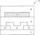
请继续参考图2与图3,其为图1位于浮动栅极静电防护元件的区域放大示意图,并一并参考图1。图2绘示了本实施例的浮动栅极静电防护元件的上视示意图,图3绘示了本实施例的浮动栅极静电防护元件沿图2的A-A’剖线的剖面示意图。如图2与图3所示,各浮动栅极静电防护元件20包括一导电图案层(例如一金属图案层)22、一介电层24、一半导体图案层(例如一非晶硅层)26,连接相邻的第一感测垫16S或是第二感测垫18S。此外,一绝缘层28可覆盖于浮动栅极静电防护元件20与相邻的第一感测垫16S及第二感测垫18S上,达到保护的效果。各浮动栅极静电防护元件20的半导体图案层26分别与相邻但未电连接的两个第一感测垫16S以及与相邻但未电连接的两个第二感测垫18S接触并部分重迭。导电图案层22分别与第一感测垫16S以及第二感测垫18S部分重迭。在本实施例中,导电图案层22位于显示面板12上、介电层24位于导电图案层22上、半导体图案层26位于介电层24上、第一感测垫16S与第二感测垫18S位于半导体图案层26上,且绝缘层28覆盖于第一感测垫16S、第二感测垫18S与半导体图案层26上。介电层24的材料可为各式有机或无机的介电材料,且以low-k介电材料为较佳,藉此可降低静电可能造成的损害。此外,介电层24的厚度可视需要作调整,且介电层24亦可制作成图案层,达到覆盖导电图案层22即可。在本实施例的浮动栅极静电防护元件20中,导电图案层22发挥栅极的作用、介电层24发挥栅极介电层的作用、半导体图案层26作为通道之用,而相邻但未电连接的两个第一感测垫16S以及与相邻但未电连接的两个第二感测垫18S则作为源极/漏极。藉由浮动栅极静电防护元件20的设置,当电容式触控装置10因摩擦或其它不可预期因素而使得静电荷累积在触控感测单元14时,大量的静电荷会诱发(induce)浮动栅极静电防护元件20的开启,也就是说第一感测垫16S或第二感测垫18S上大量的静电荷会耦合导电图案层22形成电位,因而开启半导体图案层26,使浮动栅极静电防护元件20得以开启。此时累积在某特定第一感测垫16S或第二感测垫18S的静电荷可快速地传导至相邻的第一感测垫16S或第二感测垫18S,而若静电荷的量仍然过多时,相邻的浮动栅极静电防护元件20仍会被诱发而开启而使静电荷继续向相邻的第一感测垫16S或第二感测垫18S传导。如此一来,可避免过大的静电将用以连接相邻两个第一感测垫16S的桥接线16B,或是用以连接相邻两个第二感测垫18S的桥接线18B烧断,而达到静电防护的功效。Please continue to refer to FIG. 2 and FIG. 3 , which are enlarged schematic diagrams of the area of the floating gate ESD protection device in FIG. 1 , and refer to FIG. 1 together. FIG. 2 shows a schematic top view of the floating gate ESD protection device of this embodiment, and FIG. 3 shows a schematic cross-sectional view of the floating gate ESD protection device of this embodiment along line A-A' in FIG. 2 . As shown in FIG. 2 and FIG. 3 , each floating gate
在上述实施例中,浮动栅极静电防护元件20的导电图案层22位于显示面板12上、介电层24位于导电图案层22上、半导体图案层26位于介电层24上,且第一感测垫16S与第二感测垫18S位于半导体图案层26上。导电图案层22可选择性地跟第二感测垫之间的桥接线18B一起制作,介电层24可选择性地跟桥接线18B与桥接线16B之间的介电层(图未示)一起制作,如此可简化制造工艺,降低制作成本,但并不以此为限。本发明的浮动栅极静电防护元件的结构并不以此为限,而可具有其它实施样态。请参考图4,并一并参考图1。图4绘示了本发明的另一实施例的浮动栅极静电防护元件的剖面示意图。如图4所示,各浮动栅极静电防护元件20的半导体图案层26位于显示面板12上、介电层24位于半导体图案层26、第一感测垫16S与第二感测垫18S(图4未示)上、导电图案层22位于介电层24上。In the above embodiment, the
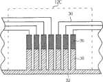
由上述可知,本发明利用设置于感测区12S内浮动栅极静电防护元件20提供电容式触控装置10所需的静电防护效果,但本发明的电容式触控装置10可于显示面板12的周边,例如连线区与连接垫区选择性地再额外设置静电防护元件,以进一步加强静电防护效果。请参考图5与图6,并一并参考图1。图5与图6绘示了本发明一较佳实施例的连线区静电防护元件的示意图,其中图5绘示了本实施例的连线区静电防护元件的上视示意图,图6绘示了本实施例的连线区静电防护元件沿图5的B-B’剖线的剖面示意图。如1图所示,电容式触控装置10的显示面板12另包括一连线区(fan out region or conductivewire region)12F、多条连接线30设置于连线区12F内、一防护环(guard ring)32设置于连线区12F内,以及多个连线区静电防护元件34。连接线30分别电连接第一感测串列16与第二感测串列18,用以传递触控感测单元14所接收到的讯号。各连线区静电防护元件34分别与一相对应的连接线30电连接以及与防护环32电连接。如图1、图5与图6所示,在本实施例中,连线区静电防护元件34为二极体静电防护元件,其包括一晶体管元件或多个晶体管元件,其中晶体管元件包括一栅极341、一介电层24、一半导体图案层26、两个源极/漏极342,343与一绝缘层28。源极/漏极342与一相对应的第一感测串列16或第二感测串列18电连接,而源极/漏极343则与栅极341以及防护环32电连接。藉由上述连接方式,晶体管元件可具有二极体元件的特性,藉此本实施例的连线区静电防护元件34可发挥静电防护作用。As can be seen from the above, the present invention uses the floating gate
请再参考图7,并一并参考图1。图7绘示了本发明另一较佳实施例的连线区静电防护元件的示意图。如图1与图7所示,本实施例的连线区静电防护元件34亦可为一浮动栅极静电防护元件,其包括一栅极341、一介电层24、一半导体图案层26、两个源极/漏极342,343与一绝缘层28,其中源极/漏极342与一相对应的第一感测串列16或第二感测串列18电连接,而源极/漏极343以及防护环32电连接。不同于前述实施例,本实施例的连线区静电防护元件34的源极/漏极343并未与栅极341电连接,但藉由上述连接方式形成的浮动栅极静电防护元件同样可有效发挥静电防护作用。Please refer to FIG. 7 again, and refer to FIG. 1 together. FIG. 7 is a schematic diagram of an electrostatic protection component in the wiring area according to another preferred embodiment of the present invention. As shown in Figures 1 and 7, the
请参考图8,并一并参考图1。图8绘示了本发明一较佳实施例的连线区静电防护元件的示意图。如1图所示,电容式触控装置10的显示面板12另包括一连接垫区(contact pad region)12C、多个连接垫36设置于连接垫区12C内,以及多个连接垫区静电防护元件38设置于连接垫区12C内。各连接垫36分别与一相对应的连接线30电连接,且各连接垫区静电防护元件38分别与一相应的连接垫36电连接。如图1与图8所示,本实施例的连接垫区静电防护元件38包括一放电尖端(discharging tip)38T,且防护环32亦包括多个放电尖端32T,分别与各连接垫区静电防护元件38的放电尖端38T相对设置,且藉由放电尖端38T,32T的设计,累积在连接垫36的静电荷可有效被传导至防护环32,防护环32可再经由接地或是其他的静电防护电路将电荷导出,达到静电防护的效果。Please refer to FIG. 8 and also refer to FIG. 1 . FIG. 8 is a schematic diagram of an electrostatic protection component in a wiring area according to a preferred embodiment of the present invention. As shown in Figure 1, the
请参考图9。图9绘示了本发明另一较佳实施例的连线区静电防护元件的示意图。如图9所示,不同于前述实施例,在本实施例中,连接垫区静电防护元件38直接与防护环32电连接,因此同样具有静电防护效果。另外,连接垫区静电防护元件38与防护环32的电连接会于后续被切断,因此在电容式触控装置实际用作时并不会使得各连接垫36之间产生短路问题。Please refer to Figure 9. FIG. 9 is a schematic diagram of an electrostatic protection component in the wiring area according to another preferred embodiment of the present invention. As shown in FIG. 9 , different from the previous embodiments, in this embodiment, the
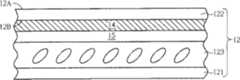
如前所述,本发明的电容式触控装置可为一具有触控输入及显示双重功能的电容式触控显示面板,或者电容式触控装置亦可单纯具有触控输入功能的电容式触控基板,并可以贴附方式与一显示面板组合而形成一电容式触控显示面板。因此依据触控显示单元设置的位置不同,本发明的电容式触控装置具有下述不同的实施样态。请参考图10。图10绘示了本发明一较佳实施例的电容式触控装置的示意图。如图10所示,显示面板12例如可为一液晶显示面板、一有机发光显示面板、一电浆显示面板、电泳显示面板等,但不限于此。本实施例以液晶显示面板为例,其包括一阵列基板121、一彩色滤光片基板122,以及一液晶层123设置于阵列基板121与彩色滤光片基板122之间。显示面板12的外侧具有一第一表面12A,例如彩色滤光片基板122的外侧表面,以及一第二表面12B,例如彩色滤光片基板122的内侧表面。显示面板12可另包括一彩色滤光层15设置于第二表面12B。在本实施例中,触控感测单元14设置于显示面板12的第一表面12A上。As mentioned above, the capacitive touch device of the present invention can be a capacitive touch display panel with dual functions of touch input and display, or the capacitive touch device can also be a capacitive touch panel with only touch input function. control substrate, and can be combined with a display panel to form a capacitive touch display panel. Therefore, according to the different positions of the touch display unit, the capacitive touch device of the present invention has the following different implementation modes. Please refer to Figure 10. FIG. 10 is a schematic diagram of a capacitive touch device according to a preferred embodiment of the present invention. As shown in FIG. 10 , the
请参考图11。图11绘示了本发明另一较佳实施例的电容式触控装置的示意图。如图11所示,在本实施例中,触控感测单元14则可设置于显示面板12的第二表面12B上。Please refer to Figure 11. FIG. 11 is a schematic diagram of a capacitive touch device according to another preferred embodiment of the present invention. As shown in FIG. 11 , in this embodiment, the
请参考图12。图12绘示了本发明又一较佳实施例的电容式触控装置的示意图。如图12所示,在本实施例中,电容式触控装置另包括一辅助基板S,其中触控感测单元14可设置于辅助基板S上,且辅助基板S可贴附于显示面板12上。Please refer to Figure 12. FIG. 12 is a schematic diagram of a capacitive touch device according to another preferred embodiment of the present invention. As shown in FIG. 12 , in this embodiment, the capacitive touch device further includes an auxiliary substrate S, wherein the
综上所述,本发明的电容式触控装置利用设置于感测区内浮动栅极静电防护元件增加静电防护能力,且进了提升静电防护能力,可进一步于连线区与连接垫区增设各种型式的静电防护元件。藉此,不论电容式触控装置为一电容式触控显示面板或一电容式触控基板,均可具有较佳的静电防护能力。To sum up, the capacitive touch device of the present invention utilizes the floating gate electrostatic protection element installed in the sensing area to increase the electrostatic protection ability, and further enhances the electrostatic protection ability, and can further increase the electrostatic protection ability in the connection area and the connection pad area. Various types of electrostatic protection components. Thereby, no matter whether the capacitive touch device is a capacitive touch display panel or a capacitive touch substrate, it can have better electrostatic protection capability.
以上所述仅为本发明的较佳实施例,凡依本发明权利要求所做的均等变化与修饰,皆应属本发明的涵盖范围。The above descriptions are only preferred embodiments of the present invention, and all equivalent changes and modifications made according to the claims of the present invention shall fall within the scope of the present invention.
Claims (20)
Priority Applications (2)
| Application Number | Priority Date | Filing Date | Title |
|---|---|---|---|
| CN201010002238ACN101763202A (en) | 2010-01-12 | 2010-01-12 | Capacitive touch display panel and capacitive touch display substrate |
| CN2010102691947ACN101907965B (en) | 2010-01-12 | 2010-08-31 | Capacitive touch display panel and capacitive touch substrate |
Applications Claiming Priority (1)
| Application Number | Priority Date | Filing Date | Title |
|---|---|---|---|
| CN201010002238ACN101763202A (en) | 2010-01-12 | 2010-01-12 | Capacitive touch display panel and capacitive touch display substrate |
Publications (1)
| Publication Number | Publication Date |
|---|---|
| CN101763202Atrue CN101763202A (en) | 2010-06-30 |
Family
ID=42494387
Family Applications (2)
| Application Number | Title | Priority Date | Filing Date |
|---|---|---|---|
| CN201010002238APendingCN101763202A (en) | 2010-01-12 | 2010-01-12 | Capacitive touch display panel and capacitive touch display substrate |
| CN2010102691947AActiveCN101907965B (en) | 2010-01-12 | 2010-08-31 | Capacitive touch display panel and capacitive touch substrate |
Family Applications After (1)
| Application Number | Title | Priority Date | Filing Date |
|---|---|---|---|
| CN2010102691947AActiveCN101907965B (en) | 2010-01-12 | 2010-08-31 | Capacitive touch display panel and capacitive touch substrate |
Country Status (1)
| Country | Link |
|---|---|
| CN (2) | CN101763202A (en) |
Cited By (13)
| Publication number | Priority date | Publication date | Assignee | Title |
|---|---|---|---|---|
| CN102096514A (en)* | 2011-02-24 | 2011-06-15 | 华映视讯(吴江)有限公司 | Touch control panel |
| CN102193676A (en)* | 2010-11-30 | 2011-09-21 | 友达光电股份有限公司 | Touch display panel, touch panel, touch element and touch circuit |
| CN102541339A (en)* | 2010-12-29 | 2012-07-04 | 东莞万士达液晶显示器有限公司 | touch display device |
| CN102890591A (en)* | 2012-09-28 | 2013-01-23 | 北京京东方光电科技有限公司 | Touch screen, touch display device and manufacturing methods of touch screen |
| CN103399670A (en)* | 2013-07-05 | 2013-11-20 | 友达光电股份有限公司 | Touch panel |
| WO2013181961A1 (en)* | 2012-06-04 | 2013-12-12 | 京东方科技集团股份有限公司 | Counter substrate and manufacturing method thereof, and touch liquid crystal display panel |
| WO2014194686A1 (en)* | 2013-06-08 | 2014-12-11 | 宸鸿科技(厦门)有限公司 | Touch control panel |
| CN104461097A (en)* | 2013-09-13 | 2015-03-25 | 恒颢科技股份有限公司 | Touch panel |
| CN104461107A (en)* | 2013-09-24 | 2015-03-25 | 胜华科技股份有限公司 | Touch panel |
| CN104571758A (en)* | 2014-12-23 | 2015-04-29 | 上海天马微电子有限公司 | Array substrate and display panel |
| CN106325585A (en)* | 2015-07-10 | 2017-01-11 | 南京瀚宇彩欣科技有限责任公司 | ESD protection touch control structure |
| WO2017215263A1 (en)* | 2016-06-17 | 2017-12-21 | Boe Technology Group Co., Ltd. | Display apparatus and fabricating method thereof |
| CN111180442A (en)* | 2020-02-06 | 2020-05-19 | 京东方科技集团股份有限公司 | Array substrate and preparation method thereof, and display device |
Families Citing this family (3)
| Publication number | Priority date | Publication date | Assignee | Title |
|---|---|---|---|---|
| TWI523180B (en)* | 2012-05-07 | 2016-02-21 | 友達光電股份有限公司 | Touch panel, touch display panel and touch display apparatus |
| TWI477851B (en) | 2012-05-22 | 2015-03-21 | Au Optronics Corp | Touch sensing display panel and touch sensing liquid crystal display panel |
| CN105022525B (en)* | 2014-04-28 | 2020-01-31 | 联咏科技股份有限公司 | Touch panel module and electrostatic discharge method thereof |
Family Cites Families (3)
| Publication number | Priority date | Publication date | Assignee | Title |
|---|---|---|---|---|
| US6175394B1 (en)* | 1996-12-03 | 2001-01-16 | Chung-Cheng Wu | Capacitively coupled field effect transistors for electrostatic discharge protection in flat panel displays |
| US20060118787A1 (en)* | 2004-12-02 | 2006-06-08 | Toppoly Optoelectronics Corp. | Electronic device with electrostatic discharge protection |
| CN101419521B (en)* | 2008-12-02 | 2010-11-03 | 友达光电股份有限公司 | Touch substrate and touch liquid crystal display |
- 2010
- 2010-01-12CNCN201010002238Apatent/CN101763202A/enactivePending
- 2010-08-31CNCN2010102691947Apatent/CN101907965B/enactiveActive
Cited By (20)
| Publication number | Priority date | Publication date | Assignee | Title |
|---|---|---|---|---|
| US8723835B2 (en) | 2010-11-30 | 2014-05-13 | Au Optronics Corporation | Touch-sensing display panel, touch panel, touch-sensing device and touch-sensing circuit |
| CN102193676A (en)* | 2010-11-30 | 2011-09-21 | 友达光电股份有限公司 | Touch display panel, touch panel, touch element and touch circuit |
| CN102541339A (en)* | 2010-12-29 | 2012-07-04 | 东莞万士达液晶显示器有限公司 | touch display device |
| CN102096514A (en)* | 2011-02-24 | 2011-06-15 | 华映视讯(吴江)有限公司 | Touch control panel |
| US9041870B2 (en) | 2012-06-04 | 2015-05-26 | Boe Technology Group Co., Ltd. | Opposed substrate, manufacturing method thereof and LCD touch panel |
| WO2013181961A1 (en)* | 2012-06-04 | 2013-12-12 | 京东方科技集团股份有限公司 | Counter substrate and manufacturing method thereof, and touch liquid crystal display panel |
| CN102890591A (en)* | 2012-09-28 | 2013-01-23 | 北京京东方光电科技有限公司 | Touch screen, touch display device and manufacturing methods of touch screen |
| WO2014194686A1 (en)* | 2013-06-08 | 2014-12-11 | 宸鸿科技(厦门)有限公司 | Touch control panel |
| CN103399670A (en)* | 2013-07-05 | 2013-11-20 | 友达光电股份有限公司 | Touch panel |
| CN103399670B (en)* | 2013-07-05 | 2017-06-06 | 友达光电股份有限公司 | Touch panel |
| CN104461097A (en)* | 2013-09-13 | 2015-03-25 | 恒颢科技股份有限公司 | Touch panel |
| CN104461097B (en)* | 2013-09-13 | 2017-11-24 | 恒颢科技股份有限公司 | Touch panel |
| CN104461107A (en)* | 2013-09-24 | 2015-03-25 | 胜华科技股份有限公司 | Touch panel |
| CN104571758A (en)* | 2014-12-23 | 2015-04-29 | 上海天马微电子有限公司 | Array substrate and display panel |
| CN106325585A (en)* | 2015-07-10 | 2017-01-11 | 南京瀚宇彩欣科技有限责任公司 | ESD protection touch control structure |
| CN106325585B (en)* | 2015-07-10 | 2019-10-18 | 南京瀚宇彩欣科技有限责任公司 | Has the touch-control structure of electrostatic protection |
| WO2017215263A1 (en)* | 2016-06-17 | 2017-12-21 | Boe Technology Group Co., Ltd. | Display apparatus and fabricating method thereof |
| US20180190598A1 (en)* | 2016-06-17 | 2018-07-05 | Boe Technology Group Co., Ltd. | Display apparatus and fabricating method thereof |
| US10515909B2 (en) | 2016-06-17 | 2019-12-24 | Boe Technology Group Co., Ltd. | Display apparatus and fabricating method thereof |
| CN111180442A (en)* | 2020-02-06 | 2020-05-19 | 京东方科技集团股份有限公司 | Array substrate and preparation method thereof, and display device |
Also Published As
| Publication number | Publication date |
|---|---|
| CN101907965B (en) | 2012-05-23 |
| CN101907965A (en) | 2010-12-08 |
Similar Documents
| Publication | Publication Date | Title |
|---|---|---|
| CN101763202A (en) | Capacitive touch display panel and capacitive touch display substrate | |
| TWI411837B (en) | Capacitive touch display panel and capacitive touch board | |
| US8952921B2 (en) | Capacitive touch display panel and capacitive touch board | |
| US8982290B2 (en) | Touch panel and touch display device | |
| TWI550458B (en) | Touch panel | |
| US9207819B2 (en) | Touch sensing display panel and touch sensing liquid crystal display panel | |
| CN102096515B (en) | touch display panel | |
| TWI472986B (en) | Touch device and electrostatic shielding method thereof | |
| TWI459253B (en) | Touch panel | |
| US20130293508A1 (en) | Touch panel, touch display panel and touch display apparatus | |
| US10222914B2 (en) | Touch device | |
| US8653382B2 (en) | Electrostatic capacitive type touch screen panel | |
| US20130229364A1 (en) | Touch display device | |
| CN204731755U (en) | Array substrate and touch display device | |
| KR20130072591A (en) | Liquid crystal display device and method for manufacturing the same | |
| KR20130110392A (en) | Liquid crystal display device and method for manufacturing the same | |
| CN102446012A (en) | Touch panel structure and touch display panel | |
| CN102129135A (en) | touch display device | |
| EP3662355B1 (en) | Touch control array substrate and touch control display apparatus | |
| CN105183204A (en) | Touch display device and touch substrate | |
| TWI528237B (en) | Touch panel and manufacturing method thereof | |
| KR20140089040A (en) | Display having touch sensing function | |
| TW201349050A (en) | Touch panel and touch sensing display using the same | |
| TW201510796A (en) | Touch panel | |
| JP3182005U (en) | Touch panel |
Legal Events
| Date | Code | Title | Description |
|---|---|---|---|
| C06 | Publication | ||
| PB01 | Publication | ||
| C10 | Entry into substantive examination | ||
| SE01 | Entry into force of request for substantive examination | ||
| C02 | Deemed withdrawal of patent application after publication (patent law 2001) | ||
| WD01 | Invention patent application deemed withdrawn after publication | Open date:20100630 |