CN101762922B - Touch type electronic paper and manufacture method thereof - Google Patents
Touch type electronic paper and manufacture method thereofDownload PDFInfo
- Publication number
- CN101762922B CN101762922BCN2008102409652ACN200810240965ACN101762922BCN 101762922 BCN101762922 BCN 101762922BCN 2008102409652 ACN2008102409652 ACN 2008102409652ACN 200810240965 ACN200810240965 ACN 200810240965ACN 101762922 BCN101762922 BCN 101762922B
- Authority
- CN
- China
- Prior art keywords
- electrode
- substrate
- film transistor
- thin film
- gate
- Prior art date
- Legal status (The legal status is an assumption and is not a legal conclusion. Google has not performed a legal analysis and makes no representation as to the accuracy of the status listed.)
- Expired - Fee Related
Links
Images


Classifications
- G—PHYSICS
- G06—COMPUTING OR CALCULATING; COUNTING
- G06F—ELECTRIC DIGITAL DATA PROCESSING
- G06F3/00—Input arrangements for transferring data to be processed into a form capable of being handled by the computer; Output arrangements for transferring data from processing unit to output unit, e.g. interface arrangements
- G06F3/01—Input arrangements or combined input and output arrangements for interaction between user and computer
- G06F3/03—Arrangements for converting the position or the displacement of a member into a coded form
- G06F3/041—Digitisers, e.g. for touch screens or touch pads, characterised by the transducing means
- G06F3/042—Digitisers, e.g. for touch screens or touch pads, characterised by the transducing means by opto-electronic means
- H—ELECTRICITY
- H10—SEMICONDUCTOR DEVICES; ELECTRIC SOLID-STATE DEVICES NOT OTHERWISE PROVIDED FOR
- H10D—INORGANIC ELECTRIC SEMICONDUCTOR DEVICES
- H10D30/00—Field-effect transistors [FET]
- H10D30/01—Manufacture or treatment
- H10D30/021—Manufacture or treatment of FETs having insulated gates [IGFET]
- H10D30/031—Manufacture or treatment of FETs having insulated gates [IGFET] of thin-film transistors [TFT]
- G—PHYSICS
- G06—COMPUTING OR CALCULATING; COUNTING
- G06F—ELECTRIC DIGITAL DATA PROCESSING
- G06F3/00—Input arrangements for transferring data to be processed into a form capable of being handled by the computer; Output arrangements for transferring data from processing unit to output unit, e.g. interface arrangements
- G06F3/01—Input arrangements or combined input and output arrangements for interaction between user and computer
- G06F3/03—Arrangements for converting the position or the displacement of a member into a coded form
- G06F3/041—Digitisers, e.g. for touch screens or touch pads, characterised by the transducing means
- G06F3/0412—Digitisers structurally integrated in a display
- H—ELECTRICITY
- H10—SEMICONDUCTOR DEVICES; ELECTRIC SOLID-STATE DEVICES NOT OTHERWISE PROVIDED FOR
- H10D—INORGANIC ELECTRIC SEMICONDUCTOR DEVICES
- H10D86/00—Integrated devices formed in or on insulating or conducting substrates, e.g. formed in silicon-on-insulator [SOI] substrates or on stainless steel or glass substrates
- H10D86/40—Integrated devices formed in or on insulating or conducting substrates, e.g. formed in silicon-on-insulator [SOI] substrates or on stainless steel or glass substrates characterised by multiple TFTs
- H10D86/60—Integrated devices formed in or on insulating or conducting substrates, e.g. formed in silicon-on-insulator [SOI] substrates or on stainless steel or glass substrates characterised by multiple TFTs wherein the TFTs are in active matrices
Landscapes
- Engineering & Computer Science (AREA)
- General Engineering & Computer Science (AREA)
- Theoretical Computer Science (AREA)
- Human Computer Interaction (AREA)
- Physics & Mathematics (AREA)
- General Physics & Mathematics (AREA)
- Thin Film Transistor (AREA)
- Liquid Crystal (AREA)
- Devices For Indicating Variable Information By Combining Individual Elements (AREA)
Abstract
Translated fromChinese
Description
Translated fromChinese技术领域technical field
本发明涉及一种电子纸及其制造方法,特别是一种触摸式电子纸及其制造方法。 The invention relates to an electronic paper and a manufacturing method thereof, in particular to a touch-type electronic paper and a manufacturing method thereof. the
背景技术Background technique
电子纸(Electronic Paper,简称E-Paper)也称数字纸,是将普通纸张显示信息的特点与计算机显示屏的特点相结合的产物。由于现有的印刷制品主要采用纸张实现,随着纸张消费量的迅速增加,对环境造成了很大的破坏。电子纸能够复制纸张的显示特点且能够重复利用,因此不会对环境造成很大的破坏,而且电子纸能够显示动态画面,因而电子纸被认为有望在不久的将来可以取代现有纸质文件。其中,基于电泳(Electrophoretic)技术的电子纸通过电泳现象来实现显示,其工作原理是利用电场分别驱动微胶囊电子墨水中带正负电荷的颜色粒子上下运动,黑白颜色粒子分别通过对自然光的反射和吸收实现黑色和白色的显示。由于电泳显示技术利用反射光进行显示,因此能耗很低。目前,基于微胶囊电子墨水的电子纸显示技术由于能耗低、显示效果与纸张接近等优点,具有广阔的应用前景。 Electronic Paper (E-Paper for short), also known as digital paper, is a product that combines the information display characteristics of ordinary paper with the characteristics of computer display screens. Since the existing printed products are mainly realized by paper, the rapid increase of paper consumption has caused great damage to the environment. Electronic paper can replicate the display characteristics of paper and can be reused, so it will not cause great damage to the environment, and electronic paper can display dynamic images, so electronic paper is expected to replace existing paper documents in the near future. Among them, electronic paper based on electrophoretic technology realizes display through electrophoretic phenomenon. Its working principle is to use electric field to drive the color particles with positive and negative charges in the microcapsule electronic ink to move up and down, and the black and white color particles respectively pass the reflection of natural light. and absorption to achieve a black and white display. Since electrophoretic display technology utilizes reflected light for display, energy consumption is very low. At present, the electronic paper display technology based on microcapsule electronic ink has broad application prospects due to its advantages of low energy consumption and display effect close to that of paper. the
内置式触摸屏(Touch Panel)近年来逐渐成为触摸屏发展的新趋势。内置式触摸屏通过将传感器制作在显示屏的内部,如直接制作在薄膜晶体管基板上,具有降低工艺复杂程度、降低显示失真和能够制作更轻更薄的器件等优点。由于电子纸显示的特点,在自然光经过微胶囊电子墨水时,自然光会被反射掉或被吸收掉,或二者都有,因此自然光不能到达薄膜晶体管基板,因此现有技术中还没有将光传感内置式触摸屏与电子纸有机结合起来的技术方案。 Built-in touch screen (Touch Panel) has gradually become a new trend in the development of touch screen in recent years. The built-in touch screen has the advantages of reducing the complexity of the process, reducing display distortion and being able to make lighter and thinner devices by making the sensor inside the display screen, such as directly on the thin film transistor substrate. Due to the characteristics of the electronic paper display, when the natural light passes through the microcapsule electronic ink, the natural light will be reflected or absorbed, or both, so the natural light cannot reach the thin film transistor substrate, so there is no light transmission in the prior art. A technical solution that organically combines a built-in touch screen with a sense of touch and electronic paper. the
发明内容Contents of the invention
本发明的目的是提供一种触摸式电子纸及其制造方法,将内置式触摸屏与电子纸有机地结合起来,具有结构简单、制备工艺简洁、成本低等优点。 The object of the present invention is to provide a touch-type electronic paper and its manufacturing method, which organically combines a built-in touch screen with the electronic paper, and has the advantages of simple structure, simple preparation process, and low cost. the
为了实现上述目的,本发明提供了一种触摸式电子纸,包括对盒的薄膜晶体管基板和透明电极基板,所述透明电极基板包括形成在第一基板上的公共电极、微胶囊电子墨水和作为光传输通道的导光柱,所述公共电极形成在第一基板上,透明材料的导光柱形成在公共电极上,所述微胶囊电子墨水涂覆在导光柱以外的公共电极上;所述薄膜晶体管基板包括形成在第二基板上的用于与透明电极基板的公共电极形成驱动微胶囊电子墨水的电场的显示电极、用于驱动所述显示电极的第一薄膜晶体管、用于探测通过所述导光柱透射的光并产生电平信号的第二薄膜晶体管和用于读取所述电平信号并发送给后端处理系统的第三薄膜晶体管,所述导光柱与所述第二薄膜晶体管相对设置。 In order to achieve the above object, the present invention provides a touch-type electronic paper, which includes a thin film transistor substrate and a transparent electrode substrate in the box, and the transparent electrode substrate includes a common electrode formed on the first substrate, microcapsule electronic ink and as The light guide column of the light transmission channel, the common electrode is formed on the first substrate, the light guide column of transparent material is formed on the common electrode, the microcapsule electronic ink is coated on the common electrode other than the light guide column; the thin film transistor The substrate includes a display electrode formed on the second substrate for forming an electric field for driving microcapsule electronic ink with the common electrode of the transparent electrode substrate, a first thin film transistor for driving the display electrode, and a first thin film transistor for detecting The light transmitted by the light column and the second thin film transistor that generates the level signal and the third thin film transistor used to read the level signal and send it to the back-end processing system, the light guide column is set opposite to the second thin film transistor . the
所述导光柱的高度为薄膜晶体管基板与透明电极基板之间间距的35%~65%。优选地,所述导光柱的高度为薄膜晶体管基板与透明电极基板之间间距的50%。 The height of the light guide column is 35%-65% of the distance between the thin film transistor substrate and the transparent electrode substrate. Preferably, the height of the light guide column is 50% of the distance between the thin film transistor substrate and the transparent electrode substrate. the
所述第一薄膜晶体管包括: The first thin film transistor includes:
第一栅电极,形成在第二基板上,并与第一栅线连接; The first gate electrode is formed on the second substrate and connected to the first gate line;
栅绝缘层,形成在第一栅电极上,并覆盖整个第二基板; a gate insulating layer formed on the first gate electrode and covering the entire second substrate;
第一有源层,包括半导体层和掺杂半导体层,形成在栅绝缘层上,并位于第一栅电极上方; The first active layer, including a semiconductor layer and a doped semiconductor layer, is formed on the gate insulating layer and located above the first gate electrode;
第一源电极,一端位于第一有源层上,另一端与数据线连接; The first source electrode, one end is located on the first active layer, and the other end is connected to the data line;
第一漏电极,一端位于第一有源层上,另一端与显示电极连接; The first drain electrode, one end is located on the first active layer, and the other end is connected to the display electrode;
第一TFT沟道区域,形成在第一源电极与第一漏电极之间,第一源电极与第一漏电极之间的掺杂半导体层被完全刻蚀掉,露出半导体层; The first TFT channel region is formed between the first source electrode and the first drain electrode, and the doped semiconductor layer between the first source electrode and the first drain electrode is completely etched away to expose the semiconductor layer;
钝化层,形成在第一源电极和第一漏电极上,并覆盖整个第二基板,其上开设有使显示电极与第一漏电极连接的钝化层过孔。 The passivation layer is formed on the first source electrode and the first drain electrode, and covers the entire second substrate, and a passivation layer via hole for connecting the display electrode and the first drain electrode is opened on it. the
所述第二薄膜晶体管包括: The second thin film transistor includes:
第二栅电极,形成在第二基板上,并与第二栅线连接; The second gate electrode is formed on the second substrate and connected to the second gate line;
栅绝缘层,形成在第二栅电极上,并覆盖整个第二基板; a gate insulating layer formed on the second gate electrode and covering the entire second substrate;
第二有源层,包括半导体层和掺杂半导体层,形成在栅绝缘层上,并位于第二栅电极上方; The second active layer, including a semiconductor layer and a doped semiconductor layer, is formed on the gate insulating layer and is located above the second gate electrode;
第二源电极,一端位于第二有源层上,另一端与电源线连接; The second source electrode, one end is located on the second active layer, and the other end is connected to the power line;
第二漏电极,一端位于第二有源层上,另一端与第三薄膜晶体管的第三源电极连接; The second drain electrode, one end is located on the second active layer, and the other end is connected to the third source electrode of the third thin film transistor;
第二TFT沟道区域,形成在第二源电极与第二漏电极之间,第二源电极与第二漏电极之间的掺杂半导体层被完全刻蚀掉,露出半导体层; The second TFT channel region is formed between the second source electrode and the second drain electrode, and the doped semiconductor layer between the second source electrode and the second drain electrode is completely etched away to expose the semiconductor layer;
钝化层,形成在第二源电极和第二漏电极上,并覆盖整个第二基板。 A passivation layer is formed on the second source electrode and the second drain electrode and covers the entire second substrate. the
所述第三薄膜晶体管包括: The third thin film transistor includes:
第三栅电极,形成在第二基板上,并与第三栅线连接; The third gate electrode is formed on the second substrate and connected to the third gate line;
栅绝缘层,形成在第三栅电极上,并覆盖整个第二基板; a gate insulating layer formed on the third gate electrode and covering the entire second substrate;
第三有源层,包括半导体层和掺杂半导体层,形成在栅绝缘层上,并位于第三栅电极上方; The third active layer, including a semiconductor layer and a doped semiconductor layer, is formed on the gate insulating layer and is located above the third gate electrode;
第三源电极,一端位于第三有源层上,另一端与第二薄膜晶体管的第二漏电极连接; The third source electrode, one end is located on the third active layer, and the other end is connected to the second drain electrode of the second thin film transistor;
第三漏电极,一端位于第三有源层上,另一端与信号线连接; The third drain electrode, one end is located on the third active layer, and the other end is connected to the signal line;
第三TFT沟道区域,形成在第三源电极与第三漏电极之间,第三源电极与第三漏电极之间的掺杂半导体层被完全刻蚀掉,露出半导体层; The third TFT channel region is formed between the third source electrode and the third drain electrode, and the doped semiconductor layer between the third source electrode and the third drain electrode is completely etched away to expose the semiconductor layer;
钝化层,形成在第三源电极和第三漏电极上,并覆盖整个第二基板。 A passivation layer is formed on the third source electrode and the third drain electrode and covers the entire second substrate. the
为了实现上述目的,本发明还提供了一种触摸式电子纸制造方法,包括: In order to achieve the above object, the present invention also provides a touch electronic paper manufacturing method, including:
制备透明电极基板,所述透明电极基板包括形成在第一基板上的公共电极和作为光传输通道的导光柱; Prepare a transparent electrode substrate, the transparent electrode substrate includes a common electrode formed on the first substrate and a light guide column as a light transmission channel;
制备薄膜晶体管基板,所述薄膜晶体管基板包括形成在第二基板上的用于与透明电极基板的公共电极形成驱动微胶囊电子墨水的电场的显示电极、用于驱动所述显示电极的作为驱动单元的第一薄膜晶体管、用于探测通过所 述导光柱透射的光并产生电平信号的作为光传感单元的第二薄膜晶体管和用于读取所述电平信号并发送给后端处理系统的作为信号读取单元的第三薄膜晶体管; Prepare a thin film transistor substrate, the thin film transistor substrate includes a display electrode formed on the second substrate for forming an electric field for driving microcapsule electronic ink with the common electrode of the transparent electrode substrate, and a display electrode for driving the display electrode as a driving unit The first thin film transistor used to detect the light transmitted through the light guide column and generate a level signal as a second thin film transistor as a light sensing unit, and the second thin film transistor used to read the level signal and send it to the back-end processing system The third thin film transistor as a signal reading unit;
将所述透明电极基板与薄膜晶体管基板对盒,且所述导光柱与第二薄膜晶体管相对设置, The transparent electrode substrate and the thin film transistor substrate are boxed together, and the light guide column is arranged opposite to the second thin film transistor,
其中,所述制备透明电极基板包括: Wherein, the preparation of the transparent electrode substrate includes:
在第一基板上形成公共电极; forming a common electrode on the first substrate;
在公共电极上形成作为光传输通道的导光柱; Forming a light guide column as a light transmission channel on the common electrode;
在导光柱以外的公共电极上涂覆微胶囊电子墨水。 The microcapsule electronic ink is coated on the common electrode other than the light guide column. the
所述制备薄膜晶体管基板包括: The preparation of thin film transistor substrates includes:
在基板上沉积栅金属薄膜,通过构图工艺形成包括第一栅线、第二栅线、第三栅线、公共电极线、第一栅电极、第二栅电极和第三栅电极的图形,其中,第一栅电极与第一栅线连接,第二栅电极与第二栅线连接,第三栅电极与第三栅线连接; A gate metal thin film is deposited on the substrate, and a pattern including a first gate line, a second gate line, a third gate line, a common electrode line, a first gate electrode, a second gate electrode and a third gate electrode is formed through a patterning process, wherein , the first grid electrode is connected to the first grid line, the second grid electrode is connected to the second grid line, and the third grid electrode is connected to the third grid line;
在完成上述图形的基板上依次沉积栅绝缘层、半导体层和掺杂半导体层,通过构图工艺形成包括第一有源层、第二有源层和第三有源层的图形,其中,第一有源层位于第一栅电极上方,第二有源层位于第二栅电极上方,第三有源层位于第三栅电极上方; A gate insulating layer, a semiconductor layer, and a doped semiconductor layer are sequentially deposited on the substrate with the above pattern, and a pattern including a first active layer, a second active layer, and a third active layer is formed through a patterning process, wherein the first The active layer is located above the first gate electrode, the second active layer is located above the second gate electrode, and the third active layer is located above the third gate electrode;
在完成上述图形的基板上沉积源漏金属薄膜,通过构图工艺形成包括数据线、电源线、信号线、第一源电极、第一漏电极、第一TFT沟道区域、第二源电极、第二漏电极、第二TFT沟道区域、第三源电极、第三漏电极和第三TFT沟道区域的图形,且第二漏电极与第三源电极连接; Deposit source and drain metal thin films on the substrate with the above pattern, and form data lines, power lines, signal lines, first source electrodes, first drain electrodes, first TFT channel regions, second source electrodes, and second source electrodes through a patterning process. Patterns of the second drain electrode, the second TFT channel region, the third source electrode, the third drain electrode and the third TFT channel region, and the second drain electrode is connected to the third source electrode;
在完成上述图形的基板上沉积钝化层,通过构图工艺形成包括钝化层过孔的图形,所述钝化层过孔位于第一漏电极的上方; Depositing a passivation layer on the substrate on which the above pattern is completed, forming a pattern including a passivation layer via hole through a patterning process, and the passivation layer via hole is located above the first drain electrode;
在完成上述图形的基板上沉积透明导电薄膜,通过构图工艺在显示区域形成包括显示电极的图形,所述显示电极通过钝化层过孔与第一漏电极连接。 A transparent conductive film is deposited on the substrate with the above pattern, and a pattern including a display electrode is formed in the display area through a patterning process, and the display electrode is connected to the first drain electrode through a passivation layer via hole. the
在上述技术方案基础上,所述导光柱的高度为薄膜晶体管基板与透明电极基板之间间距的35%~65%。优选地,所述导光柱的高度为薄膜晶体管基板 与透明电极基板之间间距的50%。 On the basis of the above technical solution, the height of the light guide column is 35%-65% of the distance between the thin film transistor substrate and the transparent electrode substrate. Preferably, the height of the light guide column is 50% of the distance between the thin film transistor substrate and the transparent electrode substrate. the
本发明提供了一种触摸式电子纸及其制造方法,通过在透明电极基板上设置作为光传输通道的导光柱,在薄膜晶体管基板上设置作为光传感单元的第二薄膜晶体管,使外界的自然光或亮光通过导光柱透射到薄膜晶体管基板上的第二薄膜晶体管上,将内置式触摸屏与电子纸有机地结合起来,有效解决了电子纸显示中自然光不能到达薄膜晶体管基板以至于不能使用光传感做触摸屏的技术问题。本发明具有结构简单、制备工艺简洁、成本低等优点,具有广阔的应用前景。 The invention provides a touch-type electronic paper and a manufacturing method thereof. A light guide column as a light transmission channel is arranged on a transparent electrode substrate, and a second thin film transistor as a light sensing unit is arranged on a thin film transistor substrate, so that external Natural light or bright light is transmitted to the second thin film transistor on the thin film transistor substrate through the light guide column, and the built-in touch screen is organically combined with the electronic paper, which effectively solves the problem that the natural light cannot reach the thin film transistor substrate in the electronic paper display and cannot use light transmission. A sense of technical issues with touch screens. The invention has the advantages of simple structure, simple preparation process, low cost, etc., and has broad application prospects. the
附图说明Description of drawings
图1为本发明触摸式电子纸的结构示意图; Fig. 1 is a schematic structural view of the touch electronic paper of the present invention;
图2为本发明第一薄膜晶体管的结构示意图; Fig. 2 is the structural representation of the first thin film transistor of the present invention;
图3为本发明第二薄膜晶体管和第三薄膜晶体管的结构示意图; Fig. 3 is the structural representation of the second thin film transistor and the third thin film transistor of the present invention;
图4为本发明触摸式电子纸制造方法的流程图; Fig. 4 is the flowchart of the manufacturing method of touch-type electronic paper of the present invention;
图5为本发明触摸式电子纸制造方法中制备透明电极基板的流程图; Fig. 5 is the flow chart of preparing transparent electrode substrate in the manufacturing method of touch-type electronic paper of the present invention;
图6为本发明触摸式电子纸制造方法中制备薄膜晶体管基板的流程图; Fig. 6 is the flow chart of preparing thin film transistor substrate in the manufacturing method of touch-type electronic paper of the present invention;
图7为本发明制备薄膜晶体管基板中第一次构图工艺的示意图; Figure 7 is a schematic diagram of the first patterning process in the preparation of the thin film transistor substrate in the present invention;
图8为本发明制备薄膜晶体管基板中第二次构图工艺的示意图; Figure 8 is a schematic diagram of the second patterning process in the preparation of the thin film transistor substrate in the present invention;
图9为本发明制备薄膜晶体管基板中第三次构图工艺的示意图; Figure 9 is a schematic diagram of the third patterning process in the preparation of a thin film transistor substrate in the present invention;
图10为本发明制备薄膜晶体管基板中第四次构图工艺的示意图; 10 is a schematic diagram of the fourth patterning process in the preparation of a thin film transistor substrate in the present invention;
图11为本发明制备薄膜晶体管基板中第五次构图工艺的示意图。 FIG. 11 is a schematic diagram of the fifth patterning process in the preparation of a thin film transistor substrate according to the present invention. the
附图标记说明: Explanation of reference signs:
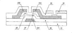
11-第一基板; 12-公共电极; 13-导光柱; 11-first substrate; 12-common electrode; 13-light guide column;
14-微胶囊电子墨水; 21-第二基板; 22-显示电极; 14-microcapsule electronic ink; 21-second substrate; 22-display electrode;
23-第一薄膜晶体管; 24-第二薄膜晶体管; 25-第三薄膜晶体管; 23-the first thin film transistor; 24-the second thin film transistor; 25-the third thin film transistor;
26-栅绝缘层; 27-半导体层; 28-掺杂半导体层; 26-gate insulating layer; 27-semiconductor layer; 28-doped semiconductor layer;
29-钝化层; 231-第一栅电极; 232-第一源电极; 29-passivation layer; 231-the first gate electrode; 232-the first source electrode;
233-第一漏电极; 241-第二栅电极; 242-第二源电极; 233-the first drain electrode; 241-the second gate electrode; 242-the second source electrode;
243-第二漏电极; 251-第三栅电极; 252-第三源电极; 243-the second drain electrode; 251-the third gate electrode; 252-the third source electrode;
253-第三漏电极; 291-钝化层过孔; 100-透明电极基板; 253-the third drain electrode; 291-passivation layer via hole; 100-transparent electrode substrate;
200-薄膜晶体管基板。 200 - thin film transistor substrate. the
具体实施方式Detailed ways
下面通过附图和实施例,对本发明的技术方案做进一步的详细描述。 The technical solutions of the present invention will be described in further detail below with reference to the accompanying drawings and embodiments. the
图1为本发明触摸式电子纸的结构示意图。如图1所示,本发明触摸式电子纸的主体结构包括透明电极基板100和薄膜晶体管基板200,透明电极基板100和薄膜晶体管基板200对盒封装成本发明触摸式电子纸。透明电极基板100包括形成在第一基板11上的公共电极12、导光柱13和微胶囊电子墨水14,公共电极12形成在第一基板11上,导光柱13形成在公共电极12上,是一种作为光传输通道的透明结构,使透明电极基板100外侧的自然光通过该导光柱13透射到薄膜晶体管基板200上,微胶囊电子墨水14也涂覆在公共电极12上,具体地说,微胶囊电子墨水14涂覆在导光柱以外的公共电极12表面上。薄膜晶体管基板200包括形成在第二基板21上的显示电极22、第一薄膜晶体管23、第二薄膜晶体管24和第三薄膜晶体管25。其中,显示电极22形成在第二基板21上,用于与透明电极基板100的公共电极12形成驱动微胶囊电子墨水14的电场;第一薄膜晶体管23形成在第二基板21上,作为驱动单元,用于控制显示电极22上的电压;第二薄膜晶体管24形成在第二基板21上,作为光传感单元,用于探测通过导光柱13透射的光,产生反映光变化的电平信号,第二薄膜晶体管24与透明电极基板100的导光柱13相对设置,即导光柱13与第二薄膜晶体管24的位置对准;第三薄膜晶体管25也形成在第二基板21上,作为信号读取单元,用于将第二薄膜晶体管24的电平信号读取出来,发送给后端处理系统,以最终获得触摸点位置, 从而控制电子纸的显示。 FIG. 1 is a schematic structural diagram of the touch electronic paper of the present invention. As shown in FIG. 1 , the main structure of the touch electronic paper of the present invention includes a
本发明上述技术方案中,透明电极基板中的第一基板可以采用玻璃基板或石英基板等透明基板,公共电极可以采用氧化铟锡(ITO)或氧化铟锌(IZO)等导电薄膜,通过磁控溅射或热蒸发方法沉积形成;导光柱为透明材料,其结构形式与现有液晶显示器中的柱状隔垫物(Post Spacer,简称PS)的结构形式相近,通过构图工艺形成。实际应用中,本发明导光柱的高度可以设置成薄膜晶体管基板与透明电极基板之间间距的35%~65%,即导光柱的高度为本发明触摸式电子纸盒厚的35%~65%。优选地,导光柱的高度为薄膜晶体管基板与透明电极基板之间间距的50%。 In the above technical solution of the present invention, the first substrate in the transparent electrode substrate can be a transparent substrate such as a glass substrate or a quartz substrate, and the common electrode can be a conductive film such as indium tin oxide (ITO) or indium zinc oxide (IZO). It is deposited and formed by sputtering or thermal evaporation; the light guide column is a transparent material, and its structure is similar to that of the post spacer (PS) in the existing liquid crystal display, and is formed through a patterning process. In practical applications, the height of the light guide column of the present invention can be set to 35% to 65% of the distance between the thin film transistor substrate and the transparent electrode substrate, that is, the height of the light guide column is 35% to 65% of the thickness of the touch electronic paper box of the present invention . Preferably, the height of the light guide column is 50% of the distance between the thin film transistor substrate and the transparent electrode substrate. the
本发明上述技术方案中,薄膜晶体管基板包括第一栅线、第二栅线、第三栅线、公共电极线、数据线、电源线、信号线、显示电极、作为驱动单元的第一薄膜晶体管、作为光传感单元的第二薄膜晶体管和作为信号读取单元的第三薄膜晶体管。具体地,第一栅线和数据线一起限定了显示区域,第一薄膜晶体管形成在第一栅线与数据线的交叉处,第二薄膜晶体管形成在第二栅线与电源线的交叉处,第三薄膜晶体管形成在第三栅线与信号线的交叉处,显示电极形成在显示区域内,公共电极线(也称存储电容线)也形成在显示区域内,位于二条第一栅线之间,用于与显示电极一起构成存储电容。 In the above technical solution of the present invention, the thin film transistor substrate includes a first gate line, a second gate line, a third gate line, a common electrode line, a data line, a power line, a signal line, a display electrode, and a first thin film transistor as a driving unit. , the second thin film transistor as the light sensing unit and the third thin film transistor as the signal reading unit. Specifically, the first gate line and the data line together define the display area, the first thin film transistor is formed at the intersection of the first gate line and the data line, and the second thin film transistor is formed at the intersection of the second gate line and the power line, The third thin film transistor is formed at the intersection of the third gate line and the signal line, the display electrode is formed in the display area, and the common electrode line (also called storage capacitor line) is also formed in the display area, located between the two first gate lines , used to form a storage capacitor together with the display electrodes. the
图2为本发明第一薄膜晶体管的结构示意图。如图2所示,第一薄膜晶体管包括第一栅电极231、栅绝缘层26、第一有源层(包括半导体层27和掺杂半导体层28)、第一源电极232、第一漏电极233和钝化层29,第一栅电极231形成在第二基板21上并与第一栅线连接;栅绝缘层26形成在第一栅电极231上并覆盖整个第二基板21;第一有源层形成在栅绝缘层26上并位于第一栅电极231的上方;第一源电极232的一端位于第一有源层上,另一端与数据线连接,第一漏电极233的一端位于第一有源层上,另一端通过钝化层过孔与显示电极22连接,第一源电极232与第一漏电极233之间形成第一TFT沟道区域,第一TFT沟道区域内的掺杂半导体层28被完全刻蚀掉,并 刻蚀掉部分厚度的半导体层27;钝化层29形成在第一TFT沟道区域上并覆盖整个第二基板21,其上开设有使显示电极22与第一漏电极233连接的钝化层过孔。本发明第一薄膜晶体管的结构形式与现有液晶显示器中薄膜晶体管的结构形式基板相同。 FIG. 2 is a schematic structural diagram of the first thin film transistor of the present invention. As shown in FIG. 2, the first thin film transistor includes a
图3为本发明第二薄膜晶体管和第三薄膜晶体管的结构示意图。如图3所示,第二薄膜晶体管包括第二栅电极241、栅绝缘层26、第二有源层(包括半导体层27和掺杂半导体层28)、第二源电极242、第二漏电极243和钝化层29,第二栅电极241形成在第二基板21上并与第二栅线连接;栅绝缘层26形成在第二栅电极241上并覆盖整个第二基板21;第二有源层形成在栅绝缘层26上并位于第二栅电极241的上方;第二源电极242的一端位于第二有源层上,另一端与电源线连接,第二漏电极243的一端位于第二有源层上,另一端与第三薄膜晶体管的第三源电极252连接,第二源电极242与第二漏电极243之间形成第二TFT沟道区域,第二TFT沟道区域内的掺杂半导体层28被完全刻蚀掉,并刻蚀掉部分厚度的半导体层27;钝化层29形成在第二TFT沟道区域上并覆盖整个第二基板21。电源线用于向第二源电极242提供电压信号,第二TFT沟道区域用于探测光的变化,使第二源电极242与第二漏电极243导通或断开。 FIG. 3 is a schematic structural diagram of a second thin film transistor and a third thin film transistor of the present invention. As shown in FIG. 3, the second thin film transistor includes a
第三薄膜晶体管包括第三栅电极251、栅绝缘层26、第三有源层(包括半导体层27和掺杂半导体层28)、第三源电极252、第三漏电极253和钝化层29,第三栅电极251形成在第二基板21上并与第三栅线连接;栅绝缘层26形成在第三栅电极251上并覆盖整个第二基板21;第三有源层形成在栅绝缘层26上并位于第三栅电极251的上方;第三源电极252的一端位于第三有源层上,另一端与第二薄膜晶体管的第二漏电极243连接,第三漏电极253的一端位于第三有源层上,另一端与信号线连接,第三源电极252与第三漏电极253之间形成第三TFT沟道区域。信号线用于将第二薄膜晶体管的电平信号发送给后端处理系统。 The third thin film transistor includes a
本发明触摸式电子纸的工作原理具体为:当没有任何触摸物触摸本发明触摸式电子纸的表面时,透明电极基板外侧的自然光或亮光通过透明电极基板上的导光柱透射到薄膜晶体管基板上的第二薄膜晶体管上,第二薄膜晶体管的光生载流子浓度没有变化;当手指等触摸物划过本发明触摸式电子纸的表面时,透明电极基板外侧的自然光或亮光被阻挡,使自然光或亮光不能到达薄膜晶体管基板上的第二薄膜晶体管,第二薄膜晶体管的光生载流子浓度将发生变化,第二薄膜晶体管的电平信号发生变化,后端处理系统通过对电平信号进行分析,即可确定触摸点的位置,从而控制电子纸的显示。 The working principle of the touch electronic paper of the present invention is specifically: when no touch object touches the surface of the touch electronic paper of the present invention, the natural light or bright light outside the transparent electrode substrate is transmitted to the thin film transistor substrate through the light guide column on the transparent electrode substrate On the second thin film transistor, the photogenerated carrier concentration of the second thin film transistor does not change; when a touch object such as a finger slides across the surface of the touch electronic paper of the present invention, the natural light or bright light outside the transparent electrode substrate is blocked, so that the natural light Or bright light cannot reach the second thin film transistor on the thin film transistor substrate, the photogenerated carrier concentration of the second thin film transistor will change, the level signal of the second thin film transistor will change, and the back-end processing system will analyze the level signal , the position of the touch point can be determined, so as to control the display of the electronic paper. the
本发明第一薄膜晶体管的工作原理与现有技术液晶显示器中薄膜晶体管的工作原理相同,不再赘述。本发明第二薄膜晶体管的第二栅电极由第二栅线提供关断电压,源电极由电源线提供正向高电平,当没有任何触摸物触摸本发明触摸式电子纸的表面时,由于外界的自然光或亮光能够通过导光柱到达第二薄膜晶体管的第二TFT沟道区域,使第二TFT沟道区域的半导体层中产生光生载流子,虽然此时第二栅电极为关断电压,但半导体层中光生载流子的存在使第二薄膜晶体管的第二源电极与第二漏电极之间导通,因此第二漏电极具有与第二源电极相同的高电平。当手指等触摸物划过本发明触摸式电子纸的表面时,透明电极基板外侧的自然光或亮光被阻挡,使自然光或亮光不能到达薄膜晶体管基板上的第二薄膜晶体管,第二TFT沟道区域半导体层中的光生载流子将消失,使第二薄膜晶体管的第二源电极与第二漏电极之间在第二栅电极关断电压的作用下断开,此时第二漏电极的电平将下降成低电平。本发明第三薄膜晶体管的第三栅电极由第三栅线提供开启电压,使第三薄膜晶体管的第三源电极与第三漏电极之间一直处于导通状态,由于第三薄膜晶体管的源电极与第二薄膜晶体管的第二漏电极连接,因此第二薄膜晶体管中第二漏电极的电平变化可以由第三薄膜晶体管的第三漏电极向信号线输出,后端的处理系统根据该电平变化就可以进行分析处理,最终获得触摸点位置,从而控制电子纸的显示。由此可见,本发明具有结构简单、制备工 艺简洁、成本低等优点,具有广阔的应用前景。 The working principle of the first thin film transistor of the present invention is the same as that of the thin film transistor in the prior art liquid crystal display, and will not be repeated here. The second gate electrode of the second thin film transistor of the present invention is provided with an off voltage by the second gate line, and the source electrode is provided with a positive high level by the power line. When no touch object touches the surface of the touch electronic paper of the present invention, due to External natural light or bright light can reach the second TFT channel region of the second thin film transistor through the light guide column, so that photogenerated carriers are generated in the semiconductor layer of the second TFT channel region, although the second gate electrode is at the off voltage at this time , but the presence of photo-generated carriers in the semiconductor layer makes the second source electrode and the second drain electrode of the second thin film transistor conduction, so the second drain electrode has the same high level as the second source electrode. When a touch object such as a finger crosses the surface of the touch electronic paper of the present invention, the natural light or bright light outside the transparent electrode substrate is blocked, so that the natural light or bright light cannot reach the second thin film transistor on the thin film transistor substrate, the second TFT channel area The photo-generated carriers in the semiconductor layer will disappear, so that the second source electrode and the second drain electrode of the second thin film transistor are disconnected under the action of the second gate electrode off voltage, and at this time, the electric current of the second drain electrode level will fall to low level. The third gate electrode of the third thin film transistor of the present invention is provided with a turn-on voltage by the third gate line, so that the third source electrode and the third drain electrode of the third thin film transistor are always in a conduction state, because the source electrode of the third thin film transistor The electrode is connected to the second drain electrode of the second thin film transistor, so the level change of the second drain electrode in the second thin film transistor can be output to the signal line by the third drain electrode of the third thin film transistor, and the processing system at the back end The level change can be analyzed and processed, and finally the position of the touch point can be obtained, so as to control the display of the electronic paper. It can be seen that the present invention has the advantages of simple structure, simple preparation process, low cost, etc., and has broad application prospects. the
图4为本发明触摸式电子纸制造方法的流程图,具体为: Fig. 4 is a flow chart of the manufacturing method of touch-type electronic paper of the present invention, specifically:
步骤1、制备透明电极基板,所述透明电极基板包括形成在第一基板上的公共电极和作为光传输通道的导光柱; Step 1, preparing a transparent electrode substrate, the transparent electrode substrate includes a common electrode formed on the first substrate and a light guide column as a light transmission channel;
步骤2、制备薄膜晶体管基板,所述薄膜晶体管基板包括形成在第二基板上的显示电极、作为驱动单元的第一薄膜晶体管、作为光传感单元的第二薄膜晶体管和作为信号读取单元的第三薄膜晶体管; Step 2, preparing a thin film transistor substrate, the thin film transistor substrate includes display electrodes formed on the second substrate, a first thin film transistor as a driving unit, a second thin film transistor as a light sensing unit and a signal reading unit a third thin film transistor;
步骤3、将所述透明电极基板与薄膜晶体管基板对盒,且所述导光柱与第二薄膜晶体管相对设置。 Step 3, aligning the transparent electrode substrate and the thin film transistor substrate, and setting the light guide column opposite to the second thin film transistor. the
首先需要说明的是,本发明触摸式电子纸制造方法中,步骤1和步骤2是相互独立的制作工艺,二者之间没有任何时序关系,可以根据实际需要按照任何次序执行步骤1和步骤2。 First of all, it should be explained that, in the manufacturing method of touch-type electronic paper of the present invention, step 1 and step 2 are mutually independent manufacturing processes, and there is no sequence relationship between them, and step 1 and step 2 can be performed in any order according to actual needs . the
图5为本发明触摸式电子纸制造方法中制备透明电极基板的流程图,具体为: Fig. 5 is a flow chart of preparing a transparent electrode substrate in the touch-type electronic paper manufacturing method of the present invention, specifically:
步骤11、在第一基板上形成公共电极;
步骤12、在公共电极上形成作为光传输通道的导光柱;
步骤13、在导光柱以外的公共电极上涂覆微胶囊电子墨水。
制备透明电极基板中,第一基板可以采用玻璃基板或石英基板等透明基板;公共电极通过磁控溅射或热蒸发方法沉积形成,公共电极可以采用氧化铟锡(ITO)或氧化铟锌(IZO)等导电薄膜;在公共电极上形成导光柱的制备方法与现有液晶显示器中制备柱状隔垫物的方法相同,透明材料的导光柱的结构形式与现有液晶显示器中的柱状隔垫物的结构形式相近;最后通过在导光柱以外的公共电极上涂覆微胶囊电子墨水,并对微胶囊电子墨水进行封装,完成本发明透明电极基板的制备。本发明导光柱的高度可以设置成薄膜晶体管基板与透明电极基板之间间距的35%~65%,即导光柱的高度为本发明触摸式电子纸盒厚的35%~65%。优选地,导光柱的高度为薄膜晶体管基板与 透明电极基板之间间距的50%。 In preparing the transparent electrode substrate, the first substrate can be a transparent substrate such as a glass substrate or a quartz substrate; the common electrode is deposited and formed by magnetron sputtering or thermal evaporation, and the common electrode can be indium tin oxide (ITO) or indium zinc oxide (IZO ) and other conductive films; the preparation method of forming a light guide column on the common electrode is the same as the method for preparing a columnar spacer in an existing liquid crystal display, and the structure of the light guide column of a transparent material is the same as that of the columnar spacer in an existing liquid crystal display. The structure forms are similar; finally, the preparation of the transparent electrode substrate of the present invention is completed by coating the microcapsule electronic ink on the common electrode other than the light guide column and encapsulating the microcapsule electronic ink. The height of the light guide column of the present invention can be set to 35% to 65% of the distance between the thin film transistor substrate and the transparent electrode substrate, that is, the height of the light guide column is 35% to 65% of the thickness of the touch electronic paper box of the present invention. Preferably, the height of the light guide column is 50% of the distance between the thin film transistor substrate and the transparent electrode substrate. the
图6为本发明触摸式电子纸制造方法中制备薄膜晶体管基板的流程图,具体为: Figure 6 is a flow chart of preparing a thin film transistor substrate in the touch electronic paper manufacturing method of the present invention, specifically:
步骤21、在基板上沉积栅金属薄膜,通过构图工艺形成包括第一栅线、第二栅线、第三栅线、公共电极线、第一栅电极、第二栅电极和第三栅电极的图形,其中,第一栅电极与第一栅线连接,第二栅电极与第二栅线连接,第三栅电极与第三栅线连接;
步骤22、在完成步骤21的基板上依次沉积栅绝缘层、半导体层和掺杂半导体层,通过构图工艺形成包括第一有源层、第二有源层和第三有源层的图形,其中,第一有源层位于第一栅电极上方,第二有源层位于第二栅电极上方,第三有源层位于第三栅电极上方;
步骤23、在完成步骤22的基板上沉积源漏金属薄膜,通过构图工艺形成包括数据线、电源线、信号线、第一源电极、第一漏电极、第一TFT沟道区域、第二源电极、第二漏电极、第二TFT沟道区域、第三源电极、第三漏电极和第三TFT沟道区域的图形,且第二漏电极与第三源电极连接;
步骤24、在完成步骤23的基板上沉积钝化层,通过构图工艺形成包括钝化层过孔的图形,所述钝化层过孔位于第一漏电极的上方;
步骤25、在完成步骤24的基板上沉积透明导电薄膜,通过构图工艺在显示区域形成包括显示电极的图形,所述显示电极通过钝化层过孔与第一漏电极连接。
图7为本发明制备薄膜晶体管基板中第一次构图工艺的示意图。步骤21中,首先,采用磁控溅射或热蒸发的方法,在第二基板(如玻璃基板或石英基板)21上沉积一层栅金属薄膜,栅金属薄膜可以使用钼、铝、铝镍合金、钼钨合金、铬或铜等金属,或使用上述几种材料组成的多层金属薄膜结构。采用普通掩模板通过第一次构图工艺对栅金属薄膜进行构图,形成包括第一栅线、第二栅线、第三栅线、公共电极线、第一栅电极231、第二栅电极241 和第三栅电极251的图形,如图7所示。其中,第一栅电极231、第二栅电极241和第三栅电极251分别作为第一薄膜晶体管、第二薄膜晶体管和第一薄膜晶体管的栅电极,第一栅电极231与第一栅线连接,第二栅电极241与第二栅线连接,第三栅电极251与第三栅线连接。 FIG. 7 is a schematic diagram of the first patterning process in the preparation of a thin film transistor substrate according to the present invention. In
图8为本发明制备薄膜晶体管基板中第二次构图工艺的示意图。步骤22中,在完成上述图形的基板上,采用等离子体增强化学气相沉积(简称PECVD)方法依次沉积栅绝缘层26、半导体层27和掺杂半导体层28。采用普通掩模板通过第二次构图工艺对半导体层27和掺杂半导体层28进行构图,形成包括第一有源层、第二有源层和第三有源层的图形,每个有源层包括半导体层27和掺杂半导体层28,如图8所示。其中,第一有源层形成在第一栅电极231上方,第二有源层形成在第二栅电极241上方,第三有源层形成在第三栅电极251上方。 FIG. 8 is a schematic diagram of the second patterning process in preparing a thin film transistor substrate according to the present invention. In
图9为本发明制备薄膜晶体管基板中第三次构图工艺的示意图。步骤23中,在完成上述图形的基板上,采用磁控溅射或热蒸发的方法沉积一层源漏金属薄膜,源漏金属薄膜可以使用钼、铝、铝镍合金、钼钨合金、铬或铜等金属,或使用上述几种材料组成的多层金属薄膜结构。采用普通掩模板通过第三次构图工艺对源漏金属薄膜进行构图,同时形成包括数据线、电源线、信号线、第一源电极232、第一漏电极233、第二源电极242、第二漏电极243、第三源电极252和第三漏电极253的图形,如图9所示。其中,第一源电极232的一端位于第一有源层上,另一端与数据线连接,第一漏电极233的一端位于第一有源层上,另一端用于与显示电极连接,第一源电极232与第一漏电极233之间形成第一TFT沟道区域,第一TFT沟道区域内的掺杂半导体层28被完全刻蚀掉,并刻蚀掉部分厚度的半导体层27;第二源电极242的一端位于第二有源层上,另一端与电源线连接,第二漏电极243的一端位于第二有源层上,另一端与第三源电极252连接,第二源电极242与第二漏电极243之间形成第二TFT沟道区域,第二TFT沟道区域内的掺杂半导体层28 被完全刻蚀掉,并刻蚀掉部分厚度的半导体层27,电源线用于向第二源电极242提供电压信号,第二TFT沟道区域用于探测光的变化,使第二源电极242与第二漏电极243导通或断开;第三源电极252的一端位于第三有源层上,另一端与第二漏电极243连接,第三漏电极253的一端位于第三有源层上,另一端与信号线连接,第三源电极252与第三漏电极253之间形成第三TFT沟道区域,第三TFT沟道区域内的掺杂半导体层28被完全刻蚀掉,并刻蚀掉部分厚度的半导体层27,信号线用于将电平信号发送给后端处理系统。 FIG. 9 is a schematic diagram of the third patterning process in preparing a thin film transistor substrate according to the present invention. In
图10为本发明制备薄膜晶体管基板中第四次构图工艺的示意图。步骤24中,在完成上述图形的基板上,采用PECVD方法沉积一层钝化层29,钝化层29可以采用氮化硅、氧化硅或氮氧化硅等材料。采用普通掩模板通过第四次构图工艺对钝化层29进行构图,形成包括钝化层过孔291的图形,钝化层过孔291位于第一漏电极233的上方,如图10所示。本次构图工艺中,还同时形成有第一栅线接口区域、第二栅线接口区域、第三栅线接口区域、数据线接口区域、电源线接口区域、信号线接口区域和公共电极线接口区域等图形,采用普通掩模板通过构图工艺形成各接口区域图形的工艺已广泛应用于目前的构图工艺中,这里不再赘述。 FIG. 10 is a schematic diagram of the fourth patterning process in preparing a thin film transistor substrate according to the present invention. In
图11为本发明制备薄膜晶体管基板中第五次构图工艺的示意图。步骤25中,在完成上述图形的基板上,采用磁控溅射或热蒸发的方法沉积一层透明导电薄膜,透明导电薄膜可以采用氧化铟锡、氧化铟锌或氧化铝锌等材料。采用普通掩模板通过第五次构图工艺对透明导电薄膜进行构图,在像素区域形成包括显示电极22的图形,显示电极22通过钝化层过孔与第一漏电极233连接,如图11所示。 FIG. 11 is a schematic diagram of the fifth patterning process in the preparation of a thin film transistor substrate according to the present invention. In
以上所说明的五次构图工艺仅仅是制备本发明薄膜晶体管基板的一种实现方法,实际使用中还可以通过增加或减少构图工艺次数、选择不同的材料或材料组合来实现本发明。例如,可以将前述第二次构图工艺和第三次构图工艺合并成一个构图工艺,通过多步刻蚀工艺,形成本发明薄膜晶体管基板。 The five-time patterning process described above is only one implementation method for preparing the thin film transistor substrate of the present invention. In actual use, the present invention can also be realized by increasing or decreasing the number of patterning processes and selecting different materials or combinations of materials. For example, the foregoing second patterning process and the third patterning process can be combined into one patterning process, and the thin film transistor substrate of the present invention can be formed through a multi-step etching process. the
将透明电极基板与薄膜晶体管基板对盒中包括涂覆封框胶和对盒封装等流程,可以采用现有液晶显示器中对盒封装的方法,保证透明电极基板上的导光柱与薄膜晶体管基板的第二薄膜晶体管对准,使透明电极基板外侧的自然光通过该导光柱透射到第二薄膜晶体管的TFT沟道区域上。 The process of boxing the transparent electrode substrate and the thin film transistor substrate includes coating the sealant and packaging the box. The existing method of box packaging in the liquid crystal display can be used to ensure the light guide column on the transparent electrode substrate and the thin film transistor substrate. The second thin film transistor is aligned so that the natural light outside the transparent electrode substrate is transmitted to the TFT channel region of the second thin film transistor through the light guide column. the
本发明提供了一种触摸式电子纸及其制造方法,通过在透明电极基板上设置作为光传输通道的导光柱,在薄膜晶体管基板上设置作为光传感单元的第二薄膜晶体管,使外界的自然光或亮光通过导光柱透射到薄膜晶体管基板上的第二薄膜晶体管上,将内置式触摸屏与电子纸有机地结合起来,有效解决了电子纸显示中自然光不能到达薄膜晶体管基板以至于不能使用光传感做触摸屏的技术问题。本发明具有结构简单、制备工艺简洁、成本低等优点,具有广阔的应用前景。 The invention provides a touch-type electronic paper and a manufacturing method thereof. A light guide column as a light transmission channel is arranged on a transparent electrode substrate, and a second thin film transistor as a light sensing unit is arranged on a thin film transistor substrate, so that external Natural light or bright light is transmitted to the second thin film transistor on the thin film transistor substrate through the light guide column, and the built-in touch screen is organically combined with the electronic paper, which effectively solves the problem that the natural light cannot reach the thin film transistor substrate in the electronic paper display and cannot use light transmission. A sense of technical issues with touch screens. The invention has the advantages of simple structure, simple preparation process, low cost, etc., and has broad application prospects. the
最后应说明的是:以上实施例仅用以说明本发明的技术方案而非限制,尽管参照较佳实施例对本发明进行了详细说明,本领域的普通技术人员应当理解,可以对本发明的技术方案进行修改或者等同替换,而不脱离本发明技术方案的精神和范围。 Finally, it should be noted that: the above embodiments are only used to illustrate the technical solutions of the present invention without limitation, although the present invention has been described in detail with reference to the preferred embodiments, those of ordinary skill in the art should understand that the technical solutions of the present invention can be Modifications or equivalent replacements can be made without departing from the spirit and scope of the technical solutions of the present invention. the
Claims (10)
Translated fromChinesePriority Applications (3)
| Application Number | Priority Date | Filing Date | Title |
|---|---|---|---|
| CN2008102409652ACN101762922B (en) | 2008-12-24 | 2008-12-24 | Touch type electronic paper and manufacture method thereof |
| US12/557,319US8569758B2 (en) | 2008-12-24 | 2009-09-10 | Touching-type electronic paper and method for manufacturing the same |
| US14/035,277US8940560B2 (en) | 2008-12-24 | 2013-09-24 | Method for manufacturing touching-type electronic paper |
Applications Claiming Priority (1)
| Application Number | Priority Date | Filing Date | Title |
|---|---|---|---|
| CN2008102409652ACN101762922B (en) | 2008-12-24 | 2008-12-24 | Touch type electronic paper and manufacture method thereof |
Publications (2)
| Publication Number | Publication Date |
|---|---|
| CN101762922A CN101762922A (en) | 2010-06-30 |
| CN101762922Btrue CN101762922B (en) | 2012-05-30 |
Family
ID=42264710
Family Applications (1)
| Application Number | Title | Priority Date | Filing Date |
|---|---|---|---|
| CN2008102409652AExpired - Fee RelatedCN101762922B (en) | 2008-12-24 | 2008-12-24 | Touch type electronic paper and manufacture method thereof |
Country Status (2)
| Country | Link |
|---|---|
| US (2) | US8569758B2 (en) |
| CN (1) | CN101762922B (en) |
Families Citing this family (18)
| Publication number | Priority date | Publication date | Assignee | Title |
|---|---|---|---|---|
| KR101611418B1 (en)* | 2010-05-06 | 2016-04-12 | 삼성전자주식회사 | Optical touch panel and method of fabricating the same |
| TWI478125B (en)* | 2011-04-01 | 2015-03-21 | E Ink Holdings Inc | A display with a touch panel |
| CN102654664B (en)* | 2011-09-13 | 2015-01-07 | 北京京东方光电科技有限公司 | Embedded capacitive type touch panel and preparation method thereof |
| TWI457681B (en)* | 2011-09-30 | 2014-10-21 | E Ink Holdings Inc | Electronic paper display |
| US9201542B2 (en) | 2012-01-19 | 2015-12-01 | E Ink Holdings Inc. | Light sensitive display apparatus and operating method thereof |
| KR101955336B1 (en)* | 2012-03-13 | 2019-03-07 | 삼성전자주식회사 | Photo-sensing transistor, method of manufacturing the same and display panel employing the photo-sensing transistor |
| US9296223B2 (en)* | 2012-03-30 | 2016-03-29 | Samsung Electronics Co., Ltd. | Electronic paper and printing device |
| TWI478033B (en) | 2012-09-07 | 2015-03-21 | E Ink Holdings Inc | Capacitive structure of capacitive touch panel |
| JP6184489B2 (en)* | 2013-06-07 | 2017-08-23 | 富士フイルム株式会社 | Composition for forming gate insulating film, organic thin film transistor, electronic paper, display device |
| CN103972241B (en)* | 2014-04-17 | 2017-02-08 | 京东方科技集团股份有限公司 | Array substrate of electronic paper, manufacturing method thereof and electronic paper |
| CN104201106A (en)* | 2014-08-26 | 2014-12-10 | 湖南普照爱伯乐平板显示器件有限公司 | Thin film transistor, and method as well as system for producing same |
| KR102226601B1 (en)* | 2014-12-02 | 2021-03-15 | 삼성디스플레이 주식회사 | Touch panel and method of manufacturing the same |
| CN105070738B (en) | 2015-08-13 | 2018-06-29 | 京东方科技集团股份有限公司 | Display panel and its manufacturing method, display device and its control method |
| CN106648210B (en)* | 2016-10-19 | 2023-11-28 | 合肥鑫晟光电科技有限公司 | Display panel, preparation method and display device thereof |
| CN107608112A (en)* | 2017-09-21 | 2018-01-19 | 重庆秉为科技有限公司 | The display of dot structure and its dot structure |
| WO2019191126A1 (en)* | 2018-03-26 | 2019-10-03 | Christopher Harrison | Touch-sensing system including a touch-sensitive paper |
| TWI653566B (en) | 2018-03-27 | 2019-03-11 | 虹彩光電股份有限公司 | Cholesterol liquid crystal writing board |
| US20200265629A1 (en)* | 2019-02-20 | 2020-08-20 | Universal City Studios Llc | Systems and methods for animation on structural features using electronic ink |
Citations (1)
| Publication number | Priority date | Publication date | Assignee | Title |
|---|---|---|---|---|
| CN1345026A (en)* | 2000-08-31 | 2002-04-17 | 精工爱普生株式会社 | Electrophoretic display |
Family Cites Families (40)
| Publication number | Priority date | Publication date | Assignee | Title |
|---|---|---|---|---|
| US5838414A (en)* | 1995-12-30 | 1998-11-17 | Samsung Display Devices Co., Ltd. | LCD device with improved resilient adhesive spacers |
| US6583846B1 (en)* | 1999-04-14 | 2003-06-24 | Hitachi, Ltd. | Liquid crystal display device with spacer covered with an electrode |
| US6493050B1 (en)* | 1999-10-26 | 2002-12-10 | International Business Machines Corporation | Wide viewing angle liquid crystal with ridge/slit pretilt, post spacer and dam structures and method for fabricating same |
| JP4785300B2 (en)* | 2001-09-07 | 2011-10-05 | 株式会社半導体エネルギー研究所 | Electrophoretic display device, display device, and electronic device |
| KR100488953B1 (en)* | 2001-12-31 | 2005-05-11 | 비오이 하이디스 테크놀로지 주식회사 | A method for forming post spacer of lcd device |
| KR20030067125A (en)* | 2002-02-07 | 2003-08-14 | 비오이 하이디스 테크놀로지 주식회사 | Lcd device having post spacer built-in type plastic substrate |
| JP3787839B2 (en)* | 2002-04-22 | 2006-06-21 | セイコーエプソン株式会社 | Device manufacturing method, device and electronic apparatus |
| US7190008B2 (en)* | 2002-04-24 | 2007-03-13 | E Ink Corporation | Electro-optic displays, and components for use therein |
| GB0229226D0 (en)* | 2002-12-14 | 2003-01-22 | Koninkl Philips Electronics Nv | Liquid crystal displays with post spacers, and their manufacture |
| US7023016B2 (en)* | 2003-07-02 | 2006-04-04 | Samsung Electronics Co., Ltd. | Thin film transistor array panel and manufacturing method thereof |
| US8058652B2 (en)* | 2004-10-28 | 2011-11-15 | Semiconductor Energy Laboratory Co., Ltd. | Semiconductor device used as electro-optical device having channel formation region containing first element, and source or drain region containing second element |
| US8003449B2 (en)* | 2004-11-26 | 2011-08-23 | Semiconductor Energy Laboratory Co., Ltd. | Method of manufacturing a semiconductor device having a reverse staggered thin film transistor |
| WO2006117909A1 (en)* | 2005-04-28 | 2006-11-09 | Sharp Kabushiki Kaisha | Pattern thin film, method for manufacturing semiconductor element and circuit board, resist material, semiconductor element and circuit board |
| US9318053B2 (en)* | 2005-07-04 | 2016-04-19 | Semiconductor Energy Laboratory Co., Ltd. | Semiconductor device and driving method thereof |
| JP5207583B2 (en)* | 2005-07-25 | 2013-06-12 | キヤノン株式会社 | Radiation detection apparatus and radiation detection system |
| CN101313352B (en)* | 2005-11-25 | 2011-11-16 | 夏普株式会社 | Display device |
| JP4940778B2 (en) | 2006-06-20 | 2012-05-30 | セイコーエプソン株式会社 | Electronic display device |
| JP2008020669A (en)* | 2006-07-13 | 2008-01-31 | Hitachi Displays Ltd | Transflective liquid crystal display device |
| US7736936B2 (en)* | 2006-08-29 | 2010-06-15 | Semiconductor Energy Laboratory Co., Ltd. | Method of forming display device that includes removing mask to form opening in insulating film |
| EP1895545B1 (en)* | 2006-08-31 | 2014-04-23 | Semiconductor Energy Laboratory Co., Ltd. | Liquid crystal display device |
| JP5116277B2 (en)* | 2006-09-29 | 2013-01-09 | 株式会社半導体エネルギー研究所 | Semiconductor device, display device, liquid crystal display device, display module, and electronic apparatus |
| TWI514347B (en)* | 2006-09-29 | 2015-12-21 | Semiconductor Energy Lab | Display device and electronic device |
| US8018568B2 (en)* | 2006-10-12 | 2011-09-13 | Cambrios Technologies Corporation | Nanowire-based transparent conductors and applications thereof |
| EP2082436B1 (en)* | 2006-10-12 | 2019-08-28 | Cambrios Film Solutions Corporation | Nanowire-based transparent conductors and method of making them |
| CN100432770C (en)* | 2006-11-29 | 2008-11-12 | 北京京东方光电科技有限公司 | A liquid crystal display apparatus |
| US9052550B2 (en)* | 2006-11-29 | 2015-06-09 | Beijing Boe Optoelectronics Technology Co., Ltd | Thin film transistor liquid crystal display |
| WO2008069162A1 (en)* | 2006-12-05 | 2008-06-12 | Semiconductor Energy Laboratory Co., Ltd. | Anti-reflection film and display device |
| JP4826512B2 (en)* | 2007-03-12 | 2011-11-30 | セイコーエプソン株式会社 | Display device and electronic device |
| US20090122282A1 (en)* | 2007-05-21 | 2009-05-14 | Nikon Corporation | Exposure apparatus, liquid immersion system, exposing method, and device fabricating method |
| JP5388500B2 (en)* | 2007-08-30 | 2014-01-15 | 株式会社半導体エネルギー研究所 | Method for manufacturing semiconductor device |
| CN101809489B (en)* | 2007-09-26 | 2013-03-27 | 夏普株式会社 | Illumination device and display device |
| CN101398562B (en)* | 2007-09-28 | 2011-02-16 | 北京京东方光电科技有限公司 | Colorful film substrate and method for manufacturing same |
| JP5275608B2 (en)* | 2007-10-19 | 2013-08-28 | 株式会社半導体エネルギー研究所 | Method for manufacturing semiconductor substrate |
| US20090115741A1 (en)* | 2007-11-06 | 2009-05-07 | Wintek Corporation | Touch sensor and touch screen panel |
| JP4924393B2 (en)* | 2007-12-05 | 2012-04-25 | ソニー株式会社 | Display device |
| JP5301240B2 (en)* | 2007-12-05 | 2013-09-25 | 株式会社ジャパンディスプレイウェスト | Display device |
| JP4553002B2 (en)* | 2007-12-05 | 2010-09-29 | ソニー株式会社 | Display device |
| WO2010024008A1 (en)* | 2008-08-29 | 2010-03-04 | シャープ株式会社 | Coordinate sensor, electronic device, display device, and light-receiving unit |
| KR102246127B1 (en)* | 2009-10-08 | 2021-04-29 | 가부시키가이샤 한도오따이 에네루기 켄큐쇼 | Semiconductor device |
| WO2011118741A1 (en)* | 2010-03-26 | 2011-09-29 | Semiconductor Energy Laboratory Co., Ltd. | Method for manufacturing semiconductor device |
- 2008
- 2008-12-24CNCN2008102409652Apatent/CN101762922B/ennot_activeExpired - Fee Related
- 2009
- 2009-09-10USUS12/557,319patent/US8569758B2/enactiveActive
- 2013
- 2013-09-24USUS14/035,277patent/US8940560B2/enactiveActive
Patent Citations (1)
| Publication number | Priority date | Publication date | Assignee | Title |
|---|---|---|---|---|
| CN1345026A (en)* | 2000-08-31 | 2002-04-17 | 精工爱普生株式会社 | Electrophoretic display |
Non-Patent Citations (2)
| Title |
|---|
| JP特开2002-149115A 2002.05.24 |
| JP特开2008-3124A 2008.01.10 |
Also Published As
| Publication number | Publication date |
|---|---|
| US8940560B2 (en) | 2015-01-27 |
| US20100155731A1 (en) | 2010-06-24 |
| US20140024152A1 (en) | 2014-01-23 |
| CN101762922A (en) | 2010-06-30 |
| US8569758B2 (en) | 2013-10-29 |
Similar Documents
| Publication | Publication Date | Title |
|---|---|---|
| CN101762922B (en) | Touch type electronic paper and manufacture method thereof | |
| US20180149900A1 (en) | Manufacturing method for tft substrate and tft substrate manufactured by the manufacturing method thereof | |
| CN102736325B (en) | A kind of dot structure and manufacture method, display device | |
| CN105895581A (en) | TFT substrate manufacturing method | |
| CN202976027U (en) | Touch display device and display part | |
| CN102520539B (en) | Touch control display device | |
| CN105607321B (en) | Touch display device and manufacturing method thereof | |
| CN104238804A (en) | Touch display device and manufacturing method thereof | |
| CN105448933B (en) | For the array substrate and preparation method thereof in liquid crystal display panel | |
| CN101305338A (en) | display device | |
| CN103531608A (en) | Touch organic light emitting diode display device and manufacturing method thereof | |
| CN104317097A (en) | COA (color filter on array) substrate, production method thereof and display device | |
| CN104123054A (en) | Touch display device | |
| US20190079626A1 (en) | Pressure-Sensitive Display Panel, Manufacturing Method Thereof and Pressure-Sensitive Display Device | |
| CN101819344A (en) | Color filter touch substrate | |
| CN102033379B (en) | Liquid crystal display and manufacturing method thereof | |
| CN105629545A (en) | Touch panel and manufacturing method thereof | |
| CN107316875A (en) | Preparation method, array base palte and the liquid crystal panel of array base palte | |
| WO2020113623A1 (en) | Touch display device | |
| CN105629546A (en) | Touch panel and manufacturing method thereof | |
| CN110047850A (en) | A kind of tft array substrate, preparation method and its display panel | |
| CN204203576U (en) | Display device | |
| US9726923B2 (en) | Touch liquid crystal display module having polarizer film comprising compensating layer, polarization layer, and polarization-protective layer | |
| CN103048840A (en) | Array substrate, manufacture method of array substrate, liquid crystal display panel and display device | |
| WO2014180052A1 (en) | Color filter substrate, indium tin oxide film with patterned configure thereof, manufacturing method thereof and liquid crystal display |
Legal Events
| Date | Code | Title | Description |
|---|---|---|---|
| C06 | Publication | ||
| PB01 | Publication | ||
| C10 | Entry into substantive examination | ||
| SE01 | Entry into force of request for substantive examination | ||
| C14 | Grant of patent or utility model | ||
| GR01 | Patent grant | ||
| CF01 | Termination of patent right due to non-payment of annual fee | Granted publication date:20120530 | |
| CF01 | Termination of patent right due to non-payment of annual fee |