CN101751344B - A compression status bit cache and backing store - Google Patents
A compression status bit cache and backing storeDownload PDFInfo
- Publication number
- CN101751344B CN101751344BCN200910224067.2ACN200910224067ACN101751344BCN 101751344 BCN101751344 BCN 101751344BCN 200910224067 ACN200910224067 ACN 200910224067ACN 101751344 BCN101751344 BCN 101751344B
- Authority
- CN
- China
- Prior art keywords
- data
- memory
- cache
- access
- unit
- Prior art date
- Legal status (The legal status is an assumption and is not a legal conclusion. Google has not performed a legal analysis and makes no representation as to the accuracy of the status listed.)
- Active
Links
Images


Classifications
- G—PHYSICS
- G06—COMPUTING OR CALCULATING; COUNTING
- G06F—ELECTRIC DIGITAL DATA PROCESSING
- G06F12/00—Accessing, addressing or allocating within memory systems or architectures
- G06F12/02—Addressing or allocation; Relocation
- G06F12/08—Addressing or allocation; Relocation in hierarchically structured memory systems, e.g. virtual memory systems
- G06F12/0802—Addressing of a memory level in which the access to the desired data or data block requires associative addressing means, e.g. caches
- G06F12/0806—Multiuser, multiprocessor or multiprocessing cache systems
- G06F12/0813—Multiuser, multiprocessor or multiprocessing cache systems with a network or matrix configuration
- G—PHYSICS
- G06—COMPUTING OR CALCULATING; COUNTING
- G06F—ELECTRIC DIGITAL DATA PROCESSING
- G06F12/00—Accessing, addressing or allocating within memory systems or architectures
- G—PHYSICS
- G06—COMPUTING OR CALCULATING; COUNTING
- G06F—ELECTRIC DIGITAL DATA PROCESSING
- G06F12/00—Accessing, addressing or allocating within memory systems or architectures
- G06F12/02—Addressing or allocation; Relocation
- G06F12/08—Addressing or allocation; Relocation in hierarchically structured memory systems, e.g. virtual memory systems
- G06F12/0802—Addressing of a memory level in which the access to the desired data or data block requires associative addressing means, e.g. caches
- G06F12/0875—Addressing of a memory level in which the access to the desired data or data block requires associative addressing means, e.g. caches with dedicated cache, e.g. instruction or stack
- G—PHYSICS
- G06—COMPUTING OR CALCULATING; COUNTING
- G06F—ELECTRIC DIGITAL DATA PROCESSING
- G06F12/00—Accessing, addressing or allocating within memory systems or architectures
- G06F12/02—Addressing or allocation; Relocation
- G06F12/08—Addressing or allocation; Relocation in hierarchically structured memory systems, e.g. virtual memory systems
- G06F12/10—Address translation
- G06F12/1009—Address translation using page tables, e.g. page table structures
- G—PHYSICS
- G06—COMPUTING OR CALCULATING; COUNTING
- G06F—ELECTRIC DIGITAL DATA PROCESSING
- G06F12/00—Accessing, addressing or allocating within memory systems or architectures
- G06F12/02—Addressing or allocation; Relocation
- G06F12/08—Addressing or allocation; Relocation in hierarchically structured memory systems, e.g. virtual memory systems
- G06F12/10—Address translation
- G06F12/1027—Address translation using associative or pseudo-associative address translation means, e.g. translation look-aside buffer [TLB]
- G06F12/1045—Address translation using associative or pseudo-associative address translation means, e.g. translation look-aside buffer [TLB] associated with a data cache
- G—PHYSICS
- G06—COMPUTING OR CALCULATING; COUNTING
- G06F—ELECTRIC DIGITAL DATA PROCESSING
- G06F12/00—Accessing, addressing or allocating within memory systems or architectures
- G06F12/02—Addressing or allocation; Relocation
- G06F12/08—Addressing or allocation; Relocation in hierarchically structured memory systems, e.g. virtual memory systems
- G06F12/12—Replacement control
- G06F12/121—Replacement control using replacement algorithms
- G06F12/128—Replacement control using replacement algorithms adapted to multidimensional cache systems, e.g. set-associative, multicache, multiset or multilevel
- G—PHYSICS
- G06—COMPUTING OR CALCULATING; COUNTING
- G06F—ELECTRIC DIGITAL DATA PROCESSING
- G06F12/00—Accessing, addressing or allocating within memory systems or architectures
- G06F12/02—Addressing or allocation; Relocation
- G06F12/08—Addressing or allocation; Relocation in hierarchically structured memory systems, e.g. virtual memory systems
- G—PHYSICS
- G06—COMPUTING OR CALCULATING; COUNTING
- G06F—ELECTRIC DIGITAL DATA PROCESSING
- G06F2212/00—Indexing scheme relating to accessing, addressing or allocation within memory systems or architectures
- G06F2212/10—Providing a specific technical effect
- G06F2212/1016—Performance improvement
- G06F2212/1024—Latency reduction
- G—PHYSICS
- G06—COMPUTING OR CALCULATING; COUNTING
- G06F—ELECTRIC DIGITAL DATA PROCESSING
- G06F2212/00—Indexing scheme relating to accessing, addressing or allocation within memory systems or architectures
- G06F2212/40—Specific encoding of data in memory or cache
- G06F2212/401—Compressed data
Landscapes
- Engineering & Computer Science (AREA)
- Theoretical Computer Science (AREA)
- Physics & Mathematics (AREA)
- General Engineering & Computer Science (AREA)
- General Physics & Mathematics (AREA)
- Mathematical Physics (AREA)
- Memory System Of A Hierarchy Structure (AREA)
- Memory System (AREA)
Abstract
Description
Translated fromChinese技术领域technical field
本发明一般地涉及存储器系统且更特别地涉及压缩状态位高速缓存和后备存储件。The present invention relates generally to memory systems and more particularly to compressed status bit caches and backing stores.
背景技术Background technique
性能要求不断地在通常包括一个或多个处理器芯片和接附的存储器设备的数据处理系统中增加。处理器芯片包括片上数据处理资源和配置为使处理资源能够访问片外的接附的存储器的存储器接口电路。系统性能通常由片上数据处理性能和对接附的存储器设备的可用带宽确定。Performance requirements continue to increase in data processing systems, which typically include one or more processor chips and attached memory devices. The processor chip includes on-chip data processing resources and memory interface circuitry configured to enable the processing resources to access off-chip attached memory. System performance is typically determined by on-chip data processing performance and available bandwidth to attached memory devices.
用于增加可用存储器带宽的一种技术是在两个或更多存储器分区上交错存储器访问。当多个片上客户端访问在每个分区中的存储器时,相关的访问请求可以排程以优化特定参数,例如总体系统吞吐量或者对特定客户端的平均等待时间。诸如片上数据处理资源的存储器系统的客户端可以通过交换的网络将存储器访问请求发布给一个或多个存储器分区。与存储器访问请求相关的物理地址使用对给定的分区配置特定的地址映射功能转换成本地分区地址。One technique for increasing available memory bandwidth is to interleave memory accesses across two or more memory partitions. When multiple on-chip clients access memory in each partition, the associated access requests can be scheduled to optimize certain parameters, such as overall system throughput or average latency for a particular client. Clients of the memory system, such as on-chip data processing resources, may issue memory access requests to one or more memory partitions over the switched network. The physical address associated with a memory access request is translated to a local partition address using an address mapping function specific to a given partition configuration.
为了进一步改善存储器带宽,一些数据可以以压缩的格式存储,这减少了表示原始数据的块所需要的位的数目。分配为以压缩的格式存储原始数据的块的存储器的数量相比较未压缩的格式没有减少,但存储和获取压缩的数据的块所需要的位的数目减少,并因此减少了存储器带宽。基于特定应用程序要求和是否原始数据的特定的块在可用的压缩算法下是可压缩的,可以使用多个无损和有损压缩格式。每个压缩格式有利地减少了表示存储在接附的存储器中的原始数据的块所需要的位的数目。但是,位的特定数目和怎样解释位要根据哪个压缩格式(如果有的话)用于表示原始数据的块。与每个块相关的选择的压缩格式由可压缩存储器的每个块的压缩状态位指示。为了使访问在接附的存储器中的数据的给定的块所需要的带宽最小化,驻存在处理器芯片上的存储器接口电路需要在初始化对接附的存储器的存储器访问请求之前参考与存储器的块相关的压缩状态位。To further improve memory bandwidth, some data can be stored in a compressed format, which reduces the number of bits required to represent a block of original data. The amount of memory allocated to store blocks of raw data in a compressed format is not reduced compared to an uncompressed format, but the number of bits required to store and retrieve blocks of compressed data is reduced, thereby reducing memory bandwidth. Multiple lossless and lossy compression formats may be used based on specific application requirements and whether particular blocks of raw data are compressible under available compression algorithms. Each compressed format advantageously reduces the number of bits required to represent a block of raw data stored in attached memory. However, the particular number of bits and how the bits are interpreted depends on which compression format (if any) is used to represent the block of raw data. The selected compression format associated with each block is indicated by a compression status bit for each block of the compressible memory. In order to minimize the bandwidth required to access a given block of data in the attached memory, the memory interface circuitry residing on the processor chip needs to reference the block of memory before initiating a memory access request to the attached memory Associated compression status bits.
为了使性能最大化,压缩状态位需要对存储器接口电路可用。一种方案包括在片上随机存取存储器(RAM)中存储压缩状态位,在本文称为压缩状态RAM,其中状态位直接映射到在驻存在接附的存储器中的可压缩存储器的区域中的存储器的块。在这个方案中,在压缩状态RAM中的一给定组的压缩状态位指示了在接附的存储器中的物理存储器的直接对应的块的压缩状态。当在分区中的存储器接口电路接收存储器访问请求时,存储器接口电路在初始化对接附的存储器的存储器访问请求之前查询压缩状态RAM。To maximize performance, the compressed status bits need to be available to the memory interface circuitry. One approach involves storing compressed state bits in on-chip random access memory (RAM), referred to herein as compressed state RAM, where the state bits map directly to memory in a region of compressible memory residing in attached memory of blocks. In this scheme, a given set of compression status bits in the compression status RAM indicates the compression status of the immediately corresponding block of physical memory in attached memory. When memory interface circuitry in a partition receives a memory access request, the memory interface circuitry queries the compressed state RAM before initiating the memory access request to the attached memory.
随着数据处理系统在性能上的提升和在总体能力上的扩展,总的接附的存储器也通常增加。由于片上压缩状态RAM直接映射到可压缩的接附的存储器,因此增加接附的存储器的数量意味着压缩状态RAM的大小的增加。例如,使接附的存储器的数量加倍应该导致压缩状态RAM的大小的加倍以适应潜在的压缩的存储器的额外的块。但是,就管芯面积来说,压缩状态位的片上存储装置相对昂贵,并且不像接附的存储器那样能被轻易地加倍。As data processing systems increase in performance and expand in overall capabilities, the total attached memory typically increases. Since the on-chip compressed state RAM maps directly to the compressible attached memory, increasing the amount of attached memory means an increase in the size of the compressed state RAM. For example, doubling the amount of attached memory should result in doubling the size of the compressed state RAM to accommodate the potentially extra block of compressed memory. However, on-chip storage of compressed status bits is relatively expensive in terms of die area, and cannot be easily doubled like attached memory.
因此,本领域中需要的是能够使数据处理系统支持大数量的接附的存储装置而不产生与存储大数目的直接映射的片上压缩状态位相关的管芯面积成本的技术。Accordingly, what is needed in the art are techniques that enable data processing systems to support large numbers of attached memory devices without incurring the die area costs associated with storing large numbers of direct-mapped on-chip compressed status bits.
发明内容Contents of the invention
本发明的一个实施例阐明了中间高速缓存,该中间高速缓存耦合于一个或多个客户端和外部存储器,并配置为访问驻存在该外部存储器中的存储压缩信息的至少一个数据表面和数据结构。中间高速缓存包括压缩状态位高速缓存和数据高速缓存单元,该压缩状态位高速缓存配置为高速缓存存储在外部存储器中的存储器的块的压缩信息,该数据高速缓存单元配置为响应包括来自客户端的第一存储器访问请求的高速缓存缺失,基于与第一存储器访问请求相关的且存储在压缩状态位高速缓存或者数据结构中的压缩信息从外部存储器请求压缩的数据,其中压缩的数据包括表示请求的数据的一减少组的数据。中间高速缓存也可以包括命令交叉器和数据交叉器,该命令交叉器配置为发送从客户端接收的与第一存储器访问请求相关的命令,该数据交叉器配置为发送与第一存储器访问请求相关的数据。One embodiment of the present invention sets forth an intermediate cache coupled to one or more clients and an external memory and configured to access at least one data surface and data structure storing compressed information residing in the external memory . The intermediate cache includes a compression status bit cache and a data cache unit configured to cache compression information for blocks of memory stored in the external memory and a data cache unit configured to respond to the A cache miss for a first memory access request, requesting compressed data from an external memory based on compression information associated with the first memory access request and stored in a compression status bit cache or data structure, wherein the compressed data includes information representing the request Data for a reduced set of data. The intermediate cache may also include a command interleave configured to send commands received from the client associated with the first memory access request and a data interleave configured to send commands associated with the first memory access request The data.
公开的中间高速缓存的一个优点是,由于大量工作压缩状态位后备存储件在片外的接附的存储器中,因此可以分配大数量的接附的存储器为可压缩的存储器块,而不产生相应的管芯面积成本。One advantage of the disclosed intermediate cache is that since a large number of working compression status bit backing stores are in off-chip attached memory, large amounts of attached memory can be allocated as compressible memory blocks without corresponding die area cost.
附图说明Description of drawings
为了详细地理解本发明的上述特征,对于以上简要说明的本发明,将参照实施例进行更为具体的描述,其中对一些实施例在附图中进行了图示。然而,需要注意的是,附图只是图示本发明的代表性实施例,因此不能认为附图限制了本发明的范围,本发明可以允许其他同样有效的实施例。So that the above recited features of the invention can be understood in detail, the invention, briefly described above, will now be described more particularly with reference to embodiments, some of which are illustrated in the accompanying drawings. It is to be noted, however, that the appended drawings illustrate only representative embodiments of this invention and are therefore not to be considered limiting of its scope, for the invention may admit to other equally effective embodiments.
图1是图示配置为实现本发明的一个或多个方面的计算机系统的框图;Figure 1 is a block diagram illustrating a computer system configured to implement one or more aspects of the present invention;
图2是根据本发明一个实施例的图1中的计算机系统的并行处理子系统的框图;FIG. 2 is a block diagram of a parallel processing subsystem of the computer system in FIG. 1 according to one embodiment of the present invention;
图3A是根据本发明一个实施例的在图2中的并行处理单元之一中的通用处理簇的框图;3A is a block diagram of a general processing cluster in one of the parallel processing units in FIG. 2 according to one embodiment of the present invention;
图3B是根据本发明一个实施例的在图2中的并行处理单元之一中的分区单元的框图;3B is a block diagram of a partition unit in one of the parallel processing units in FIG. 2 according to one embodiment of the present invention;
图4是根据本发明一个实施例的图3B中二级(L2)高速缓存的概念图;FIG. 4 is a conceptual diagram of the Level 2 (L2) cache in FIG. 3B according to one embodiment of the present invention;
图5是根据本发明一个实施例的虚拟地址到原始分区地址转换流水线的概念图;5 is a conceptual diagram of a virtual address to original partition address translation pipeline according to one embodiment of the present invention;
图6是根据本发明一个实施例的用于压缩数据位高速缓存的原始分区地址产生流水线的概念图;和6 is a conceptual diagram of a raw partition address generation pipeline for a compressed data bit cache according to one embodiment of the present invention; and
图7图示了相对于与接附的并行处理器存储器相关的分区的压缩状态位高速缓存后备存储件的分配。FIG. 7 illustrates the allocation of compaction status bit cache backing stores relative to partitions associated with attached parallel processor memory.
具体实施方式Detailed ways
在下文的描述中,给出了大量具体的细节以便提供对本发明更为彻底的理解。然而,对于本领域技术人员来说显而易见的是,本发明可以无需一个或多个这些具体细节而得以实施。在其他的例子中,为了避免与本发明发生混淆,对于公知的特征未进行描述。In the following description, numerous specific details are given in order to provide a more thorough understanding of the present invention. It will be apparent, however, to one skilled in the art that the present invention may be practiced without one or more of these specific details. In other instances, well-known features have not been described in order to avoid obscuring the present invention.
系统概述System Overview
图1是图示配置为实现本发明一个或多个方面的计算机系统100的框图。计算机系统100包括中央处理单元(CPU)102和系统存储器104,二者通过可以包括存储器桥105的总线路径进行通信。可以是例如北桥芯片的存储器桥105通过总线或其他通信路径106(例如HyperTransport(超传输)链路)与I/O(输入/输出)桥107相连接。I/O桥107例如可以是南桥芯片,其从一个或多个用户输入设备108(例如键盘、鼠标)接收用户输入,并将该输入通过路径106和存储器桥105转发给CPU 102。并行处理子系统112通过总线或其他通信路径113(例如PCI Express、加速图形端口或超传输链路)与存储器桥105相耦合;在一个实施例中,并行处理子系统112是将像素提供给显示设备110(例如传统的CRT或基于LCD的显示器)的图形子系统。系统盘114同样连接于I/O桥107。开关116提供了I/O桥107和诸如网络适配器118以及各种插卡120和121的其他部件之间的连接。包括USB或其他端口连接、CD驱动器、DVD驱动器、电影记录设备等的其他部件(图中没有明确示出),也可以与I/O桥107相连接。将图1中的各种部件相互连接的通信路径可以用任何适用的协议来实现,比如PCI(外设部件互连)、PCI Expres s(PCI-E)、AGP(加速图形端口)、超传输或任何其他总线或点对点通信协议,并且不同设备之间的连接可以使用不同协议,如本领域已知的。FIG. 1 is a block diagram illustrating a computer system 100 configured to implement one or more aspects of the present invention. Computer system 100 includes a central processing unit (CPU) 102 and a system memory 104 that communicate through a bus path that may include a
在一个实施例中,并行处理子系统112包括为图形和视频处理优化的电路,包括例如视频输出电路,并构成了图形处理单元(GPU)。在另一实施例中,并行处理子系统112包括为通用处理优化的电路,并保留了底层计算架构的电路,本文将更加详细地描述。在又一实施例中,并行处理子系统112可以集成一个或多个其他系统元件,例如存储器桥105、CPU 102和I/O桥107,以形成片上系统(SoC)。In one embodiment,
可以理解的是,这里示出的系统只是示意性的,可以对其进行变化和修改。包括桥的数量和排列的连接拓扑结构可以根据需要修改。例如,在一些实施例中,系统存储器104直接与CPU 102相连接而不是通过桥相连接,其他设备通过存储器桥105和CPU 102与系统存储器104相通信。在其他可选择的拓扑结构中,并行处理系统112与I/O桥107相连接或直接与CPU 102相连接,而不是和存储器桥105相连接。在其他实施例中,I/O桥107和存储器桥105可以集成到单一芯片上。这里示出的特定部件是可选的;例如,可以支持任何数量的插卡或外设。在一些实施例中,省去了开关116,网络适配器118和插卡120、121直接和I/O桥107相连接。It is to be understood that the system shown here is illustrative only and that variations and modifications are possible. The connection topology including the number and arrangement of bridges can be modified as desired. For example, in some embodiments, system memory 104 is directly connected to
图2示出了根据本发明一个实施例的并行处理子系统112。如图所示,并行处理子系统112包括一个或多个并行处理单元(PPU)202,每个并行处理单元202都和本地并行处理(PP)存储器204耦合。通常,并行处理子系统包括U个PPU,其中U≥1。(在这里,相似对象的多个例子用表明该对象的附图标记和表明该例子的附加说明数字(需要时)来表示)。PPU 202和并行处理存储器204可以使用例如可编程处理器、专用集成电路(ASIC)或存储器设备的一个或多个集成电路设备,或以任何其他技术上可行的方式来实现。Figure 2 illustrates a
再次参考图1,在一些实施例中,在并行处理子系统112中的一些或者全部的并行处理单元202是具有渲染流水线的图形处理器,其能被配置成进行与下列情形有关的各种任务:从通过CPU 102和/或系统存储器104经由存储器桥105和总线113提供的图形数据产生像素数据;与本地并行处理存储器204(其能被用作图形存储器,例如包括常规的帧缓冲器)交互以存储并更新像素数据;提供像素数据给显示设备110等。在一些实施例中,并行处理子系统112可包括作为图形处理器工作的一个或多个并行处理单元202和用于通用计算的一个或多个其他并行处理单元202。并行处理单元可以是相同或不同的,且每个并行处理单元202可以有其自己专用的并行处理存储器设备或没有专用的并行处理存储器设备。一个或多个并行处理单元202可以将数据输出到显示设备110或者每个并行处理单元202可以将数据输出到一个或多个显示设备110。Referring again to FIG. 1 , in some embodiments, some or all of the
在操作中,CPU 102是计算机系统100的主处理器,其控制和协调其他系统部件的操作。特别是,CPU 102发出控制并行处理单元202操作的命令。在一些实施例中,CPU 102将对于每个并行处理单元202的命令流写入到推入缓冲器(图1和图2中未明确地示出),该推入缓冲器可以位于系统存储器104、并行处理存储器204或是CPU 102和并行处理单元202都可以访问的另一个存储位置中。并行处理单元202从推入缓冲器中读出命令流,并且随后相对于CPU 102的操作异步地执行命令。In operation,
现在返回参考图2,每个并行处理单元202包括通过通信路径113和计算机系统100的剩余部分通信的I/O(输入/输出)单元205,该通信路径113与存储器桥105相连接(或是在一个可选实施例中直接与CPU 102相连接)。并行处理单元202和计算机系统100的剩余部分的连接也可以变化。在一些实施例中,并行处理子系统112实现为插卡,其能插入到计算机系统100的扩展槽中。在其他实施例中,并行处理单元202能和总线桥一起集成到单一芯片上,总线桥例如可以是存储器桥105或I/O桥107。在另外其他实施例中,并行处理单元202的一些或全部元件可以连同CPU102一起集成到单一芯片上。Referring back now to FIG. 2 , each
在一个实施例中,通信路径113是PCI-E链路,其中如本领域所已知的,专用通道分配给每个PPU 202。也可以使用其他通信路径。I/O单元205产生包(或其他信号)以在通信路径113上传送,并也接收所有来自通信路径113的输入包(或其他信号),并将输入包引导至PPU 202的适当的部件。例如,和处理任务有关的命令可以被引导至主机接口206,而和存储器操作有关的命令(例如从并行处理存储器204中读取或向其写入)可以被引导至存储器交叉器(crossbar)单元210。主机接口206读取每个推入缓冲器,并将由推入缓冲器指定的工作输出到前端212。In one embodiment,
每个PPU 202有利地实现高度并行处理架构。如详细示出的,PPU 202(0)包括处理簇阵列230,处理簇阵列230包括数量为C的通用处理簇(GPC)208,其中C≥1。每个GPC 208能同时执行大量(例如数百个或数千个)线程,其中每个线程是程序的实例。在不同应用中,不同的GPC 208被分配用以处理不同类型的程序或进行不同类型的计算。例如,在图形应用中,第一组GPC 208可以分配为进行镶嵌操作并产生面片的图元拓扑,而第二组GPC 208可以分配为进行镶嵌着色以评价图元拓扑的面片参数并确定顶点位置和其他每顶点属性。GPC 208的分配基于每个类型的程序或计算产生的工作量是可以变化的。Each
GPC 208通过工作分配单元200接收将要执行的处理任务,该工作分配单元200从前端单元212接收限定了处理任务的命令。处理任务包括例如表面(面片)数据、图元数据、顶点数据和/或像素数据的要处理数据的索引,还有状态参数和限定数据如何处理的命令(例如执行什么程序)。工作分配单元200可以配置成取得对应于任务的索引,或者工作分配单元200可以从前端212接收索引。前端212保证在推入缓冲器指定的处理启动前,GPC 208配置为有效状态。The
例如,当并行处理单元202用于图形处理时,每个面片的处理工作量被分成大约相等大小的任务,以使得能将镶嵌处理分配给多个GPC 208。工作分配单元200可以配置成以能提供任务到多个GPC 208以处理的频率产生任务。相反,在常规系统中,典型地由单一处理引擎实施处理,而其他处理引擎保持空闲,在开始它们的处理任务前等待该单一处理引擎完成它的任务。在本发明的一些实施例中,部分GPC 208配置成进行不同类型的处理。例如,第一部分可以配置成进行顶点着色和产生拓扑结构,第二部分可以配置成进行镶嵌和几何着色,以及第三部分可以配置成在屏幕空间上进行像素着色以产生渲染的图像。GPC 208产生的中间数据可以存储在缓冲器中以允许中间数据在GPC 208之间传输以进一步处理。For example, when
存储器接口214包括D个分区单元215,每个分区单元215与并行处理存储器204的一部分直接耦合,其中D≥1。如图所示,分区单元215的数目通常等于DRAM220的数目。在其他实施例中,分区单元215的数目可以不等于存储器设备的数目。本领域的普通技术人员可以理解的是,DRAM220可以由其他合适的存储设备代替并且通常可以是惯常的设计。因此省略了详细的描述。诸如帧缓冲器或纹理贴图的渲染目标可以跨越DRAM 220存储,允许分区单元215将每个渲染目标的部分并行写入,以有效地使用并行处理存储器204的可用带宽。
GPC 208的任何一个可以处理要写入到并行处理存储器204中的任何分区单元215中的数据。交叉器(crossbar)单元210配置为将每个GPC 208的输出发送至任何分区单元215的输入或另一GPC 208以进一步处理。GPC208通过交叉器单元210与存储器接口214通信以从各种外部存储器设备中读取或写入各种外部存储器设备。在一个实施例中,交叉器单元210与存储器接口214连接以与I/O单元205通信,交叉器单元210也和本地并行处理存储器204连接,因此使得不同GPC 208内的处理内核能与系统存储器104或对并行处理单元202为非本地的其他存储器通信。交叉器单元210可以使用虚拟通道以在GPC 208和分区单元215之间分开通信流。Any one of
此外,GPC 208能被编程以执行与广泛多种应用相关的处理任务,所述应用包括但不限于线性和非线性数据转换、视频和/或音频数据的过滤、建模操作(例如,应用物理规律来确定对象的位置、速度和其他属性)、图像渲染操作(例如,镶嵌着色器、顶点着色器、几何着色器和/或像素着色器程序)等等。并行处理单元202可以将数据从系统存储器104和/或本地并行处理存储器204传输到内部(片上)存储器,处理数据,并将结果数据写回到系统存储器104和/或本地并行处理存储器204中,其中这样的数据能够由包括CPU 102或另一并行处理子系统112的其他系统部件访问。In addition,
并行处理单元202可以提供有任意数量的本地并行处理存储器204,包括没有本地存储器,并可以以任意组合使用本地存储器和系统存储器。例如,在统一存储器架构(UMA)的实施例中,并行处理单元202可以是图形处理器。在这样的实施例中,会提供极少或者不提供专用图形(并行处理)存储器,并行处理单元202唯一地使用或几乎唯一地使用系统存储器。在UMA实施例中,并行处理单元202可被集成到桥芯片或处理器芯片中,或者是提供为具有高速链路(例如PCI-E)的分立的芯片,该高速链路将并行处理单元202通过桥芯片或其他通信装置与系统存储器相连接。
如上所述,并行处理子系统112中可以包括任意数量的并行处理单元202。例如,多个并行处理单元202可以提供在单个的插卡上,或者多个插卡可以与通信路径113相连,或者并行处理单元202的一个或多个可以集成到桥芯片中。多并行处理单元系统中的并行处理单元202可以是彼此相同的,或者可以是彼此不同的。例如,不同的并行处理单元202可以具有不同数量的处理内核、不同数量的本地并行处理存储器等等。当存在有多个并行处理单元202时,那些并行处理单元可以以高于单个并行处理单元202可能达到的吞吐量来并行操作以处理数据。包含有一个或多个并行处理单元202的系统可以以各种配置和形式因素实现,包括台式计算机、笔记本计算机、或是手持个人计算机、服务器、工作站、游戏控制台、嵌入式系统等等。As mentioned above, any number of
处理簇阵列概述Overview of Working with Clustered Arrays
图3A是根据本发明一个实施例的在图2的并行处理单元202之一中的GPC 208的框图。每个GPC 208可以配置为并行执行大量的线程,在此术语“线程”是指对一特定组的输入数据执行的特定程序的实例。在一些实施例中,单指令多数据(SIMD)指令发送技术被用于支持并行执行大量线程,而不用提供多个独立的指令单元。在其他实施例中,使用配置为向每一个GPC 208中的一组处理引擎发送指令的共同指令单元,单指令多线程(SIMT)技术被用来支持并行执行大量通常同步的线程。不像SIMD执行方式中所有处理引擎通常执行相同的指令,SIMT的执行允许不同的线程通过给定的线程程序更加容易地跟随分散的执行路径。本领域的普通技术人员可以理解的是,SIMD处理方式代表了SIMT处理方式的功能性子集。FIG. 3A is a block diagram of the
在图形应用中,GPC 208可以配置为实现图元引擎304以进行屏幕空间图形处理功能,其包括但不限于图元建立、光栅化和Z剔除。在一些实施例中,图元引擎304配置为在将像素输出到L1高速缓存320之前收集像素到多个邻近的像素的片段中,以改善L1高速缓存320的访问效率。图元引擎304从工作分配单元200接收处理任务,当处理任务不需要由图元引擎304实施的操作时,处理任务通过图元引擎304传送到流水线管理器305。GPC 208的操作通过流水线管理器305有利地控制,流水线管理器305将处理任务分配给流多处理器(SPM)310。流水线管理器305也可以配置为通过为SPM 310输出的处理的数据指定目的地来控制工作分配交叉器(crossbar)330。In graphics applications,
在一个实施例中,每个GPC 208包括M个SPM 310,其中M≥1,每个SPM 310配置成处理一个或多个线程组。此外,每个SPM 310有利地包括可以流水线化的相同组的功能单元(例如算术逻辑单元等),允许新指令在前指令完成之前发送,这已在本领域中公知。可以提供功能单元的任何组合。在一个实施例中,功能单元支持各种运算,包括整数和浮点算术(例如加法和乘法)、比较运算、布尔运算(与、或、异或)、移位和各种代数函数(例如平面插值函数、三角算法函数、指数和对数函数等)计算;并且相同的功能单元硬件可以被平衡为实施不同的运算。In one embodiment, each
传送到特定GPC 208的系列指令构成了已在本文前面定义的线程,且在SPM 310内在并行处理引擎(未示出)上一定数量同时执行的线程的集合在本文中称为“线程簇”或“线程组”。如本文所使用的,“线程组”指的是对不同输入数据同时执行相同程序的线程的组,组中的一个线程被分配给SPM 310中的不同处理引擎。线程组可以包括比SPM 310中处理引擎数量少的线程,在这种情况中,在当处理线程组时的周期期间,一些处理引擎将是空闲的。线程组也可以包括比SPM 310中处理引擎数量多的线程,在这种情况中,处理将发生在连续时钟周期上。由于每个SPM 310可以同时支持多达G个线程组,因此多达GxM个线程组可以在任何给定的时间在GPC 208中执行。A series of instructions delivered to a
另外,多个相关的线程组可以同时在SPM310中是活动的(在不同的执行阶段)。这个线程组的集合在本文中称为“合作线程阵列”(“CTA”)。特定CTA的大小等于m*k,其中k是在线程组中同时执行的线程的数目且典型地是在SPM310中并行处理引擎的数目的整数倍,m是在SPM310中同时活动的线程组的数目。CTA的大小通常由程序员和CTA可用的诸如存储器或寄存器的硬件资源的数量确定。Additionally, multiple related thread groups may be active in
每个SPM 310使用在用于进行装载和存储操作的相应的L1高速缓存320中的空间。每个SPM 310也访问所有GPC 208共享并可以用于在线程之间传送数据的分区单元215中的L2高速缓存。最后,SPM 310也访问片外“全局”存储器,其可以包括例如并行处理存储器204和/或系统存储器104。可以理解的是,并行处理单元202外部的任何存储器都可以用作全局存储器。Each
在图形应用中,GPC 208可以配置为使得每个SPM 310和纹理单元315耦合以进行纹理贴图操作,例如确定纹理样本的位置、读取纹理数据和过滤纹理数据。纹理数据从L1高速缓存320中读取并按照需要从L2高速缓存、并行处理存储器204或者系统存储器104中取得。每个SPM 310向工作分配交叉器330输出处理的任务,以向另一GPC 208提供处理的任务以做进一步处理,或通过交叉器单元210将处理的任务存储在L2高速缓存、并行处理存储器204或者系统存储器104中。颜色PreROP(预先光栅操作器)325配置成进行颜色混合的优化,组织像素颜色数据,并进行地址翻译。In graphics applications,
可以理解的是,本文描述的内核架构是示例性的,可以做变化和改变。任何数量的处理引擎,例如图元引擎304、SPM 310、纹理单元315或颜色PreROP 325可以包括在GPC 208中。进一步,虽然只示出了一个GPC 208,并行处理单元202可以包括任何数量的GPC 208,这些GPC 208功能上有利地彼此相似,使得执行行为不取决于哪个GPC 208接收了特定处理任务。进一步,每个GPC 208使用单独的和不同的处理引擎、L1高速缓存320等相对另外的GPC 208有利地独立地工作。It will be appreciated that the kernel architectures described herein are exemplary and are subject to variation and modification. Any number of processing engines, such as primitive engine 304,
图3B是根据本发明一个实施例的图2中并行处理单元202其中之一中的分区单元215的框图。如图所示,分区单元215包括L2高速缓存350、帧缓冲器(FB)355和光栅操作单元(ROP)360。L2高速缓存350是配置为进行从交叉器单元210和ROP 360接收的装载和存储操作的读/写高速缓存。在一些实施例中,L2高速缓存350可以分成四个(或更少的)片从而以帧缓冲器355四倍的带宽与存储器交叉器单元210接口。读取缺失和紧急写回请求通过L2高速缓存350输出到帧缓冲器355处理。脏(dirty)更新也送到帧缓冲器355用于机会处理。帧缓冲器355直接与并行处理存储器204接口,输出读取和写入请求,并接收从并行处理存储器204读取的数据。FIG. 3B is a block diagram of the
在图形应用中,ROP 360是进行光栅操作的处理单元,例如模板、z测试等,并将像素数据输出为处理的图形数据以存储在图形存储器中。处理的图形数据可以显示在显示设备110上,或被发送以通过CPU 102或通过并行处理子系统112中的处理实体之一来进一步处理。每个分区单元215包括ROP 360以分配光栅操作的处理。在一些实施例中,ROP 360配置为压缩写到存储器中的z或颜色数据,并将从存储器中读取的z或颜色数据解压缩。In graphics applications, the
本领域的技术人员可以理解的是,图1、2、3A和3B中描述的架构决不限制本发明的范围,本文中教导的技术可以在任何适合地配置的处理单元上实现,该处理单元包括但不限于一个或多个CPU、一个或多个多内核CPU、一个或多个并行处理单元202、一个或多个GPC 208、一个或多个图形或专用处理单元等,这些都不离开本发明的范围。Those skilled in the art will appreciate that the architectures described in Figures 1, 2, 3A, and 3B in no way limit the scope of the present invention, and that the techniques taught herein may be implemented on any suitably configured processing unit that Including but not limited to one or more CPUs, one or more multi-core CPUs, one or more
压缩状态位高速缓存和后备存储件Compressed state bit cache and backing store
图4是根据本发明一个实施例的图3B中二级(L2)高速缓存350的概念图。L2高速缓存350包括ROP交叉器410和一个或多个L2片420。在一个实施例中,四个L2片420(0)-420(3)包括在L2高速缓存350中。L2高速缓存350从交叉器单元210接收存储器访问请求并可以从至少一个ROP360接收存储器访问请求。存储器访问请求包括在可以与数据表面相关的存储器块上实施的读和写操作。至少一个ROP360将存储器访问请求提供给将该请求分配给L2片420的ROP交叉器410。在具有两个或更多诸如图2中分区单元215的分区单元的处理芯片中,交叉器单元210将存储器访问请求发送给两个或更多分区单元,每个分区单元包括L2高速缓存350的例子。FIG. 4 is a conceptual diagram of level two (L2)
在每个L2高速缓存350中的每个L2片420包括命令交叉器422、数据交叉器424、压缩状态位高速缓存426和L2数据高速缓存428。命令交叉器422将存储器访问请求的命令部分引导给压缩状态位高速缓存426。数据交叉器424通过交叉器单元210或者ROP360在压缩状态位高速缓存426和存储器客户端之间发送数据。Each L2 slice 420 in each
驻存在诸如图2的DRAM220的外部DRAM中的后备存储件包括数据结构,该数据结构应当提供足够的压缩状态位设置以指示也驻存在DRAM中的所有压缩的存储器块的压缩状态。每个压缩状态位设置指示驻存在外部DRAM中的存储器的相应块的压缩状态,该外部DRAM可以接附至帧缓冲器355。压缩状态位高速缓存426从后备存储件存储高速缓存行,其中每个高速缓存行包括多个压缩状态位设置。一个或多个高速缓存行组织为高速缓存数据存储件,设置在压缩状态位高速缓存426中。如果与来自存储器客户端的存储器访问请求相关的压缩状态位设置当前没有存储在高速缓存数据存储件中,那么产生压缩状态位高速缓存缺失。响应压缩状态位高速缓存缺失,压缩状态位高速缓存426产生对后备存储件的存储器访问请求以获取包括请求的压缩状态位设置的高速缓存行。Backing storage residing in an external DRAM, such as
在一个实施例中,两个位构成一个压缩状态位设置,其中每个压缩状态位设置能采取两个位给定的四个代码值中的一个。一个代码值可以用于指示存储器的相应的块没有压缩,而剩下的三个代码值的每个可以指示三个不同压缩格式之一。In one embodiment, two bits make up one compressed status bit setting, where each compressed status bit setting can take one of four code values given by the two bits. One code value can be used to indicate that the corresponding block of memory is not compressed, while each of the remaining three code values can indicate one of three different compression formats.
压缩状态位高速缓存426可以实施任何技术上可行的标记关联方案和任何技术上可行的逐出策略。在正常操作下,对压缩的表面的存储器访问请求将通过压缩状态位高速缓存426以为请求的存储器的块确定压缩状态。基于压缩状态,存储器访问请求转送给L2数据高速缓存428以处理。在L2数据高速缓存428中的高速缓存命中可以由L2数据高速缓存428本地地处理,而在L2数据高速缓存428中的高速缓存缺失导致存储器访问请求产生并发布给帧缓冲器355。任何技术上可行的替换策略和关联机制可以在L2数据高速缓存428中使用。Compression status bit cache 426 may implement any technically feasible tag association scheme and any technically feasible eviction strategy. Under normal operation, a memory access request to a compressed surface will pass through the compression status bit cache 426 to determine the compression status for the requested block of memory. Based on the compression status, the memory access request is forwarded to the L2 data cache 428 for processing. A cache hit in the L2 data cache 428 may be handled locally by the L2 data cache 428 , while a cache miss in the L2 data cache 428 results in a memory access request being generated and issued to the
重要地,如果L2数据高速缓存428缺失,那么只有由相应高速缓存行的压缩的表示需要的位的数目需要由L2数据高速缓存428请求。由L2数据高速缓存428启动的存储器请求所需要的位的数目由驻存在压缩状态位高速缓存426中的压缩状态位设置指示。通过将存储器请求大小限制为只包括存储器的请求的块的压缩的表示需要的位,在并行处理存储器204上需要的带宽减低了。Importantly, if the L2 data cache 428 misses, only the number of bits required by the compressed representation of the corresponding cache line needs to be requested by the L2 data cache 428 . The number of bits required for a memory request initiated by L2 data cache 428 is indicated by the compression status bit setting resident in compression status bit cache 426 . By limiting the memory request size to only include the bits required for a compressed representation of the requested block of memory, the required bandwidth on the
例如ROP360的一定的存储器客户端是知道压缩的且能够直接读和写压缩的数据。其他客户端是不知道压缩的且不能够直接处理压缩的数据。例如,图2中的GPC208通常没有能力处理压缩的数据。如果知道压缩的存储器客户端请求对存储器的压缩的块的读或写操作,那么L2高速缓存350可以用压缩的数据回应。但是如果不知道压缩的存储器客户端从存储器的压缩的块请求读,那么L2高速缓存350对在存储器的压缩的块中的数据解压缩并将解压缩的数据返回给不知道的存储器客户端。在一定的情况中,不知道压缩的存储器客户端可以只将未压缩的数据写回到存储器的任何给定的块中。Certain memory clients such as ROP360 are aware of compression and can read and write compressed data directly. Other clients are not aware of compression and cannot handle compressed data directly. For example,
图5是根据本发明一个实施例的虚拟地址到原始分区地址转换流水线500的概念图。虚拟地址到原始分区地址转换流水线500包括存储器管理单元(MMU)520、物理地址种类交换搅和(swizzle)单元(PAKS搅和器)522、除法器524、分区地址单元530、片地址单元540和L2标记、L2设置单元550。在一个实施例中,图2中的每个GPC208包括MMU单元。FIG. 5 is a conceptual diagram of a virtual address to raw partition
MMU520包括用于将虚拟地址510映射到物理地址的一组页表项(PTE)。并非限制,每个PTE包括虚拟地址到物理地址映射信息、表面种类信息和压缩标记行信息。物理地址由PAKS搅和器522处理以产生分配访问位置以允许在分区单元中有效地请求交错的搅和的物理地址。除法器产生由分区地址单元530、片地址单元540和L2标记、L2设置单元550使用的商和余数以计算唯一的DRAM地址。分区地址单元530计算用于将相应的存储器访问请求发送给图2中的一个分区单元215的分区地址532。片地址单元540计算用于将存储器访问请求发送给图4中一个选择的L2片420的片地址542。
L2标记、L2设置单元550接收包括来自除法器524的商的片特定的物理地址和偏移地址用于存储器访问请求。L2标记、L2设置单元550计算对应于可以用于访问特定DRAM220设备的原始分区地址的L2标记和L2设置552。L2标记和L2设置552也可以用于查询图4中的L2数据高速缓存428。The L2 tag, L2 set
图6是根据本发明一个实施例的压缩状态位高速缓存的原始分区地址产生流水线600的概念图。压缩状态位高速缓存(CSBC)基数610包括用于存储压缩状态位的后备存储件的偏移地址。高速缓存行号码612由加法器620算术地加到CSBC基数610以计算片特定的物理地址,该片特定的物理地址可以由L2标记、L2设置单元630处理以产生对应于可以用于访问特定DRAM220设备的原始分区地址的L2标记、L2设置地址632。L2标记、L2设置单元630对片特定的物理地址实施与图5的L2标记、L2设置单元550大致相同的计算。重要地,L2标记、L2设置单元630和L2标记、L2设置单元550都接收具有相同形式的片特定的物理地址并对片特定的物理地址实施大致相同的地址位操作以产生具有相同形式的原始分区地址。这种对称允许两个单元在相同的分区中寻址数据的块而没有地址空间冲突。在一个实施例中,原始分区地址产生流水线600在图4的压缩状态位高速缓存426中实施。FIG. 6 is a conceptual diagram of a raw partition
高速缓存行号码612从由MMU520产生的压缩标记行信息取得。高速缓存行号码612将一块压缩的存储器与一组相关的压缩状态位相关。高速缓存行号码612也作为由图4中的压缩状态位高速缓存426使用的查找标记。The
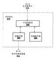
图7图示了相对于与接附的并行处理器存储器204相关的分区的压缩状态位高速缓存后备存储件700的分配。每个分区单元215包括压缩状态位高速缓存(CSBC)710,该压缩状态位高速缓存(CSBC)710配置为提供驻存在对应的CSBC后备存储件720中的压缩状态位的片上的、高速缓存的形式。每个CSBC后备存储件720配置为存储应当唯一地映射到驻存在对应的DRAM220中的数据的块的压缩状态位。例如,CSBC后备存储件720(1)包括唯一地映射到DRAM220(1)的压缩状态位。另外,CSBC710(1)高速缓存唯一地映射到CSBC后备存储件720(1)的压缩状态位。相反地,压缩的表面730和740包括分配在并行处理存储器204中的DRAM220(0)到DRAM220(D-1)的数据。FIG. 7 illustrates the allocation of the compressed state bit cache backing store 700 relative to the partitions associated with the attached
本领域的技术人员将理解的是,通过限制哪个DRAM220为驻存在相同DRAM220中的数据的块存储压缩状态位,可以防止在交叉器210上显著的额外的流量,同时保留通过在多个分区上分配正常的存储器访问请求获得的增强的存储器性能。Those skilled in the art will understand that by restricting which
总之,公开了使数据处理系统能够支持大数量的接附的存储装置而不产生管芯面积成本的技术。压缩状态位高速缓存耦合于驻存在外部存储器中的后备存储件。压缩状态位存储在后备存储件中用于存储在相同物理分区中的存储器的每个块。给定分区的后备存储件数据不应当驻存在任何其他分区中。为了避免分区地址混叠,在后备存储件中的存储器的块根据用于在给定的分区中的所有其他分区地址的相同的再映射功能再映射(“搅和”)。In summary, techniques are disclosed that enable a data processing system to support a large number of attached memory devices without incurring die area costs. The compressed status bit cache is coupled to a backing store residing in external memory. Compression status bits are stored in the backing store for each block of memory stored in the same physical partition. Backing store data for a given partition should not reside in any other partition. To avoid partition address aliasing, blocks of memory in the backing store are remapped ("scrambled") according to the same remapping function used for all other partition addresses in a given partition.
本发明的一个优点是,由于工作压缩状态位后备存储件的大部分是在片外接附的存储器中,因此大数量的接附的存储器可以分配为可压缩存储器块,而不产生相应的管芯面积成本。第二个优点是这个技术与高性能分区和基于片的虚拟存储器架构可操作。An advantage of the present invention is that since the majority of the working compressed status bit backing storage is in off-chip attached memory, large amounts of attached memory can be allocated as blocks of compressible memory without creating corresponding die area cost. A second advantage is that this technique is operable with high-performance partitioned and slice-based virtual memory architectures.
本发明的一个实施例可以实施为与计算机系统使用的程序产品。程序产品的程序限定了实施例(包括本文描述的方法)的功能且能包含在各种计算机可读存储介质中。图示的计算机可读存储介质包括但不限于:(i)其上信息被永久存储的不可写存储介质(例如,计算机中的只读存储器设备,诸如由CD-ROM驱动器可读取的CD-ROM盘、闪存、ROM芯片或任何类型的固态非易失半导体存储器);和(ii)其上存储可改变信息的可写存储介质(例如,软盘驱动器中的软盘或硬盘驱动器或任何类型的固态随机存取半导体存储器)。One embodiment of the present invention can be implemented as a program product for use with a computer system. The program(s) of the program product define functions of the embodiments (including the methods described herein) and can be contained on a variety of computer-readable storage media. Illustrative computer-readable storage media include, but are not limited to: (i) non-writable storage media on which information is permanently stored (e.g., a read-only memory device in a computer, such as a CD-ROM drive readable by a CD-ROM drive). ROM disk, flash memory, ROM chip, or any type of solid-state non-volatile semiconductor memory); and (ii) a writable storage medium on which changeable information is stored (for example, a floppy disk in a floppy disk drive or a hard disk drive or any type of solid-state random access semiconductor memory).
上面已经参考特定实施例对本发明进行了描述。但是,本领域的技术人员将理解的是,在不背离如所附的权利要求阐明的本发明的较宽的精神和范围的情况下,可以对特定实施例作出各种修改和改变。因此前述的描述和附图是示例性的而不是限制性的。The invention has been described above with reference to specific embodiments. Those skilled in the art will appreciate, however, that various modifications and changes can be made to the particular embodiments without departing from the broader spirit and scope of the invention as set forth in the appended claims. The foregoing description and drawings are therefore illustrative rather than restrictive.
Claims (10)
Applications Claiming Priority (2)
| Application Number | Priority Date | Filing Date | Title |
|---|---|---|---|
| US12/327,790 | 2008-12-03 | ||
| US12/327,790US8700862B2 (en) | 2008-12-03 | 2008-12-03 | Compression status bit cache and backing store |
Publications (2)
| Publication Number | Publication Date |
|---|---|
| CN101751344A CN101751344A (en) | 2010-06-23 |
| CN101751344Btrue CN101751344B (en) | 2013-02-27 |
Family
ID=41572646
Family Applications (1)
| Application Number | Title | Priority Date | Filing Date |
|---|---|---|---|
| CN200910224067.2AActiveCN101751344B (en) | 2008-12-03 | 2009-12-03 | A compression status bit cache and backing store |
Country Status (6)
| Country | Link |
|---|---|
| US (2) | US8700862B2 (en) |
| JP (1) | JP5142299B2 (en) |
| KR (1) | KR101102190B1 (en) |
| CN (1) | CN101751344B (en) |
| DE (1) | DE102009047200A1 (en) |
| GB (1) | GB2465876B (en) |
Families Citing this family (31)
| Publication number | Priority date | Publication date | Assignee | Title |
|---|---|---|---|---|
| US8464001B1 (en)* | 2008-12-09 | 2013-06-11 | Nvidia Corporation | Cache and associated method with frame buffer managed dirty data pull and high-priority clean mechanism |
| US8862823B1 (en)* | 2008-12-19 | 2014-10-14 | Nvidia Corporation | Compression status caching |
| US9569348B1 (en)* | 2009-09-22 | 2017-02-14 | Nvidia Corporation | Method for automatic page table compression |
| US8688655B2 (en)* | 2010-08-27 | 2014-04-01 | International Business Machines Corporation | Network analysis |
| CN102436421B (en)* | 2010-09-29 | 2015-12-16 | 腾讯科技(深圳)有限公司 | Data cached method |
| US9378560B2 (en)* | 2011-06-17 | 2016-06-28 | Advanced Micro Devices, Inc. | Real time on-chip texture decompression using shader processors |
| US8886883B1 (en)* | 2012-03-31 | 2014-11-11 | Emc Corporation | System and method for improving cache performance |
| US9244840B2 (en)* | 2012-12-12 | 2016-01-26 | International Business Machines Corporation | Cache swizzle with inline transposition |
| US9830262B2 (en)* | 2013-03-14 | 2017-11-28 | Nvidia Corporation | Access tracking mechanism for hybrid memories in a unified virtual system |
| US11228769B2 (en)* | 2013-06-03 | 2022-01-18 | Texas Instruments Incorporated | Multi-threading in a video hardware engine |
| US9582426B2 (en)* | 2013-08-20 | 2017-02-28 | International Business Machines Corporation | Hardware managed compressed cache |
| US10503661B2 (en)* | 2014-05-21 | 2019-12-10 | Qualcomm Incorporated | Providing memory bandwidth compression using compressed memory controllers (CMCs) in a central processing unit (CPU)-based system |
| US10838862B2 (en) | 2014-05-21 | 2020-11-17 | Qualcomm Incorporated | Memory controllers employing memory capacity compression, and related processor-based systems and methods |
| US9355038B2 (en)* | 2014-09-11 | 2016-05-31 | Qualcomm Incorporated | Cache bank spreading for compression algorithms |
| GB2536880B (en)* | 2015-03-24 | 2021-07-28 | Advanced Risc Mach Ltd | Memory management |
| JP6605323B2 (en)* | 2015-12-24 | 2019-11-13 | ルネサスエレクトロニクス株式会社 | Semiconductor device, data processing system, and control method of semiconductor device |
| EP3376369B1 (en) | 2016-01-20 | 2020-03-04 | Samsung Electronics Co., Ltd. | Method, apparatus and recording medium for processing division calculation |
| US10540290B2 (en)* | 2016-04-27 | 2020-01-21 | Ati Technologies Ulc | Method and apparatus for translation lookaside buffer with multiple compressed encodings |
| US10282808B2 (en)* | 2016-05-27 | 2019-05-07 | Intel Corporation | Hierarchical lossless compression and null data support |
| US9996471B2 (en)* | 2016-06-28 | 2018-06-12 | Arm Limited | Cache with compressed data and tag |
| US10387305B2 (en)* | 2016-12-23 | 2019-08-20 | Intel Corporation | Techniques for compression memory coloring |
| US10061698B2 (en) | 2017-01-31 | 2018-08-28 | Qualcomm Incorporated | Reducing or avoiding buffering of evicted cache data from an uncompressed cache memory in a compression memory system when stalled write operations occur |
| US10474468B2 (en)* | 2017-02-22 | 2019-11-12 | Advanced Micro Devices, Inc. | Indicating instruction scheduling mode for processing wavefront portions |
| CN106945406B (en)* | 2017-04-01 | 2018-06-05 | 杭州旗捷科技有限公司 | Operating method, consumable chip, consumable container, the consumptive material equipment of consumable chip |
| US10620994B2 (en) | 2017-05-30 | 2020-04-14 | Advanced Micro Devices, Inc. | Continuation analysis tasks for GPU task scheduling |
| KR20190093361A (en)* | 2018-02-01 | 2019-08-09 | 에스케이하이닉스 주식회사 | Electronic system having host and memory controller, and operating method thereof |
| US12099867B2 (en) | 2018-05-30 | 2024-09-24 | Advanced Micro Devices, Inc. | Multi-kernel wavefront scheduler |
| US10733692B2 (en)* | 2018-11-09 | 2020-08-04 | Intel Corporation | Interface apparatus and method resilient to graphics hardware changes |
| US11526445B2 (en) | 2019-05-13 | 2022-12-13 | Rambus Inc. | Managing memory maintenance operations in a memory system having backing storage media |
| US10909033B1 (en)* | 2019-08-15 | 2021-02-02 | Nvidia Corporation | Techniques for efficiently partitioning memory |
| CN115168248B (en)* | 2022-09-02 | 2022-11-25 | 北京登临科技有限公司 | Cache memory supporting SIMT architecture and corresponding processor |
Citations (1)
| Publication number | Priority date | Publication date | Assignee | Title |
|---|---|---|---|---|
| US20050144388A1 (en)* | 2003-12-31 | 2005-06-30 | Newburn Chris J. | Processor and memory controller capable of use in computing system that employs compressed cache lines' worth of information |
Family Cites Families (17)
| Publication number | Priority date | Publication date | Assignee | Title |
|---|---|---|---|---|
| US5875454A (en)* | 1996-07-24 | 1999-02-23 | International Business Machiness Corporation | Compressed data cache storage system |
| US6128094A (en)* | 1998-07-08 | 2000-10-03 | Hewlett-Packard Company | Printer having processor with instruction cache and compressed program store |
| US6640283B2 (en)* | 2002-01-16 | 2003-10-28 | Hewlett-Packard Development Company, L.P. | Apparatus for cache compression engine for data compression of on-chip caches to increase effective cache size |
| US6795897B2 (en)* | 2002-05-15 | 2004-09-21 | International Business Machines Corporation | Selective memory controller access path for directory caching |
| US7636810B2 (en)* | 2003-11-26 | 2009-12-22 | Intel Corporation | Method, system, and apparatus for memory compression with flexible in-memory cache |
| US7162584B2 (en)* | 2003-12-29 | 2007-01-09 | Intel Corporation | Mechanism to include hints within compressed data |
| US7383399B2 (en)* | 2004-06-30 | 2008-06-03 | Intel Corporation | Method and apparatus for memory compression |
| JP2006031480A (en)* | 2004-07-16 | 2006-02-02 | Sony Corp | Information processing system, information processing method, and computer program thereof |
| US7243191B2 (en)* | 2004-08-31 | 2007-07-10 | Intel Corporation | Compressing data in a cache memory |
| US7702875B1 (en)* | 2004-11-18 | 2010-04-20 | Sun Microsystems, Inc. | System and method for memory compression |
| US8473673B2 (en)* | 2005-06-24 | 2013-06-25 | Hewlett-Packard Development Company, L.P. | Memory controller based (DE)compression |
| JP4846306B2 (en)* | 2005-09-09 | 2011-12-28 | 富士通セミコンダクター株式会社 | Semiconductor memory device, semiconductor integrated circuit system using the same, and method for controlling semiconductor memory device |
| US7849256B2 (en)* | 2006-07-11 | 2010-12-07 | Advanced Micro Devices, Inc. | Memory controller with ring bus for interconnecting memory clients to memory devices |
| US8683139B2 (en)* | 2006-10-31 | 2014-03-25 | Hewlett-Packard Development Company, L.P. | Cache and method for cache bypass functionality |
| KR100849305B1 (en) | 2006-11-24 | 2008-07-29 | 삼성전자주식회사 | Memory for compressing and managing and the method |
| US7769955B2 (en)* | 2007-04-27 | 2010-08-03 | Arm Limited | Multiple thread instruction fetch from different cache levels |
| US7975109B2 (en)* | 2007-05-30 | 2011-07-05 | Schooner Information Technology, Inc. | System including a fine-grained memory and a less-fine-grained memory |
- 2008
- 2008-12-03USUS12/327,790patent/US8700862B2/enactiveActive
- 2009
- 2009-11-25GBGB0920627Apatent/GB2465876B/enactiveActive
- 2009-11-26DEDE102009047200Apatent/DE102009047200A1/ennot_activeCeased
- 2009-12-03JPJP2009275686Apatent/JP5142299B2/enactiveActive
- 2009-12-03CNCN200910224067.2Apatent/CN101751344B/enactiveActive
- 2009-12-03KRKR1020090119078Apatent/KR101102190B1/enactiveActive
- 2014
- 2014-01-16USUS14/157,159patent/US10515011B2/enactiveActive
Patent Citations (1)
| Publication number | Priority date | Publication date | Assignee | Title |
|---|---|---|---|---|
| US20050144388A1 (en)* | 2003-12-31 | 2005-06-30 | Newburn Chris J. | Processor and memory controller capable of use in computing system that employs compressed cache lines' worth of information |
Also Published As
| Publication number | Publication date |
|---|---|
| US20140237189A1 (en) | 2014-08-21 |
| GB2465876A (en) | 2010-06-09 |
| US20100138614A1 (en) | 2010-06-03 |
| US10515011B2 (en) | 2019-12-24 |
| DE102009047200A1 (en) | 2010-09-02 |
| JP5142299B2 (en) | 2013-02-13 |
| JP2010134929A (en) | 2010-06-17 |
| KR20100063674A (en) | 2010-06-11 |
| CN101751344A (en) | 2010-06-23 |
| KR101102190B1 (en) | 2012-01-02 |
| US8700862B2 (en) | 2014-04-15 |
| GB2465876B (en) | 2011-07-20 |
| GB0920627D0 (en) | 2010-01-13 |
Similar Documents
| Publication | Publication Date | Title |
|---|---|---|
| CN101751344B (en) | A compression status bit cache and backing store | |
| US8627041B2 (en) | Efficient line and page organization for compression status bit caching | |
| US8341380B2 (en) | Efficient memory translator with variable size cache line coverage | |
| US8982140B2 (en) | Hierarchical memory addressing | |
| CN101739357B (en) | Multi-class data cache policies | |
| US8917271B2 (en) | Redistribution of generated geometric primitives | |
| JP5127815B2 (en) | Avoiding deadlocks by marking CPU traffic as special | |
| US8760460B1 (en) | Hardware-managed virtual buffers using a shared memory for load distribution | |
| US8244984B1 (en) | System and method for cleaning dirty data in an intermediate cache using a data class dependent eviction policy | |
| US9589310B2 (en) | Methods to facilitate primitive batching | |
| US8271734B1 (en) | Method and system for converting data formats using a shared cache coupled between clients and an external memory | |
| US9569348B1 (en) | Method for automatic page table compression | |
| US8810592B2 (en) | Vertex attribute buffer for inline immediate attributes and constants | |
| US8595437B1 (en) | Compression status bit cache with deterministic isochronous latency | |
| US8060700B1 (en) | System, method and frame buffer logic for evicting dirty data from a cache using counters and data types | |
| US9798543B2 (en) | Fast mapping table register file allocation algorithm for SIMT processors | |
| CN103885893A (en) | Technique For Accessing Content-Addressable Memory | |
| US20130124802A1 (en) | Class Dependent Clean and Dirty Policy | |
| US9436969B2 (en) | Time slice processing of tessellation and geometry shaders | |
| US8504773B1 (en) | Storing dynamically sized buffers within a cache | |
| US8427493B2 (en) | Draw commands with built-in begin/end | |
| US8862823B1 (en) | Compression status caching | |
| US8570916B1 (en) | Just in time distributed transaction crediting | |
| US8976185B2 (en) | Method for handling state transitions in a network of virtual processing nodes | |
| US8704835B1 (en) | Distributed clip, cull, viewport transform and perspective correction |
Legal Events
| Date | Code | Title | Description |
|---|---|---|---|
| C06 | Publication | ||
| PB01 | Publication | ||
| C10 | Entry into substantive examination | ||
| SE01 | Entry into force of request for substantive examination | ||
| C14 | Grant of patent or utility model | ||
| GR01 | Patent grant |