CN101746717A - methods of forming carbon nanotubes - Google Patents
methods of forming carbon nanotubesDownload PDFInfo
- Publication number
- CN101746717A CN101746717ACN200910246780ACN200910246780ACN101746717ACN 101746717 ACN101746717 ACN 101746717ACN 200910246780 ACN200910246780 ACN 200910246780ACN 200910246780 ACN200910246780 ACN 200910246780ACN 101746717 ACN101746717 ACN 101746717A
- Authority
- CN
- China
- Prior art keywords
- carbon nanotubes
- forming
- substrate
- metal layer
- catalyst
- Prior art date
- Legal status (The legal status is an assumption and is not a legal conclusion. Google has not performed a legal analysis and makes no representation as to the accuracy of the status listed.)
- Granted
Links
Images


Classifications
- B—PERFORMING OPERATIONS; TRANSPORTING
- B82—NANOTECHNOLOGY
- B82B—NANOSTRUCTURES FORMED BY MANIPULATION OF INDIVIDUAL ATOMS, MOLECULES, OR LIMITED COLLECTIONS OF ATOMS OR MOLECULES AS DISCRETE UNITS; MANUFACTURE OR TREATMENT THEREOF
- B82B3/00—Manufacture or treatment of nanostructures by manipulation of individual atoms or molecules, or limited collections of atoms or molecules as discrete units
- B82B3/0009—Forming specific nanostructures
- C—CHEMISTRY; METALLURGY
- C23—COATING METALLIC MATERIAL; COATING MATERIAL WITH METALLIC MATERIAL; CHEMICAL SURFACE TREATMENT; DIFFUSION TREATMENT OF METALLIC MATERIAL; COATING BY VACUUM EVAPORATION, BY SPUTTERING, BY ION IMPLANTATION OR BY CHEMICAL VAPOUR DEPOSITION, IN GENERAL; INHIBITING CORROSION OF METALLIC MATERIAL OR INCRUSTATION IN GENERAL
- C23C—COATING METALLIC MATERIAL; COATING MATERIAL WITH METALLIC MATERIAL; SURFACE TREATMENT OF METALLIC MATERIAL BY DIFFUSION INTO THE SURFACE, BY CHEMICAL CONVERSION OR SUBSTITUTION; COATING BY VACUUM EVAPORATION, BY SPUTTERING, BY ION IMPLANTATION OR BY CHEMICAL VAPOUR DEPOSITION, IN GENERAL
- C23C16/00—Chemical coating by decomposition of gaseous compounds, without leaving reaction products of surface material in the coating, i.e. chemical vapour deposition [CVD] processes
- C23C16/02—Pretreatment of the material to be coated
- C23C16/0272—Deposition of sub-layers, e.g. to promote the adhesion of the main coating
- C23C16/0281—Deposition of sub-layers, e.g. to promote the adhesion of the main coating of metallic sub-layers
- B—PERFORMING OPERATIONS; TRANSPORTING
- B82—NANOTECHNOLOGY
- B82Y—SPECIFIC USES OR APPLICATIONS OF NANOSTRUCTURES; MEASUREMENT OR ANALYSIS OF NANOSTRUCTURES; MANUFACTURE OR TREATMENT OF NANOSTRUCTURES
- B82Y10/00—Nanotechnology for information processing, storage or transmission, e.g. quantum computing or single electron logic
- B—PERFORMING OPERATIONS; TRANSPORTING
- B82—NANOTECHNOLOGY
- B82Y—SPECIFIC USES OR APPLICATIONS OF NANOSTRUCTURES; MEASUREMENT OR ANALYSIS OF NANOSTRUCTURES; MANUFACTURE OR TREATMENT OF NANOSTRUCTURES
- B82Y30/00—Nanotechnology for materials or surface science, e.g. nanocomposites
- B—PERFORMING OPERATIONS; TRANSPORTING
- B82—NANOTECHNOLOGY
- B82Y—SPECIFIC USES OR APPLICATIONS OF NANOSTRUCTURES; MEASUREMENT OR ANALYSIS OF NANOSTRUCTURES; MANUFACTURE OR TREATMENT OF NANOSTRUCTURES
- B82Y40/00—Manufacture or treatment of nanostructures
- C—CHEMISTRY; METALLURGY
- C01—INORGANIC CHEMISTRY
- C01B—NON-METALLIC ELEMENTS; COMPOUNDS THEREOF; METALLOIDS OR COMPOUNDS THEREOF NOT COVERED BY SUBCLASS C01C
- C01B32/00—Carbon; Compounds thereof
- C01B32/15—Nano-sized carbon materials
- C01B32/158—Carbon nanotubes
- C01B32/16—Preparation
- C01B32/162—Preparation characterised by catalysts
- C—CHEMISTRY; METALLURGY
- C23—COATING METALLIC MATERIAL; COATING MATERIAL WITH METALLIC MATERIAL; CHEMICAL SURFACE TREATMENT; DIFFUSION TREATMENT OF METALLIC MATERIAL; COATING BY VACUUM EVAPORATION, BY SPUTTERING, BY ION IMPLANTATION OR BY CHEMICAL VAPOUR DEPOSITION, IN GENERAL; INHIBITING CORROSION OF METALLIC MATERIAL OR INCRUSTATION IN GENERAL
- C23C—COATING METALLIC MATERIAL; COATING MATERIAL WITH METALLIC MATERIAL; SURFACE TREATMENT OF METALLIC MATERIAL BY DIFFUSION INTO THE SURFACE, BY CHEMICAL CONVERSION OR SUBSTITUTION; COATING BY VACUUM EVAPORATION, BY SPUTTERING, BY ION IMPLANTATION OR BY CHEMICAL VAPOUR DEPOSITION, IN GENERAL
- C23C16/00—Chemical coating by decomposition of gaseous compounds, without leaving reaction products of surface material in the coating, i.e. chemical vapour deposition [CVD] processes
- C23C16/22—Chemical coating by decomposition of gaseous compounds, without leaving reaction products of surface material in the coating, i.e. chemical vapour deposition [CVD] processes characterised by the deposition of inorganic material, other than metallic material
- C23C16/26—Deposition of carbon only
- H—ELECTRICITY
- H10—SEMICONDUCTOR DEVICES; ELECTRIC SOLID-STATE DEVICES NOT OTHERWISE PROVIDED FOR
- H10K—ORGANIC ELECTRIC SOLID-STATE DEVICES
- H10K71/00—Manufacture or treatment specially adapted for the organic devices covered by this subclass
- H10K71/10—Deposition of organic active material
- H—ELECTRICITY
- H10—SEMICONDUCTOR DEVICES; ELECTRIC SOLID-STATE DEVICES NOT OTHERWISE PROVIDED FOR
- H10K—ORGANIC ELECTRIC SOLID-STATE DEVICES
- H10K85/00—Organic materials used in the body or electrodes of devices covered by this subclass
- H10K85/20—Carbon compounds, e.g. carbon nanotubes or fullerenes
- H10K85/221—Carbon nanotubes
Landscapes
- Chemical & Material Sciences (AREA)
- Engineering & Computer Science (AREA)
- Nanotechnology (AREA)
- Materials Engineering (AREA)
- Organic Chemistry (AREA)
- Chemical Kinetics & Catalysis (AREA)
- Crystallography & Structural Chemistry (AREA)
- Mechanical Engineering (AREA)
- General Chemical & Material Sciences (AREA)
- Metallurgy (AREA)
- Inorganic Chemistry (AREA)
- Physics & Mathematics (AREA)
- Condensed Matter Physics & Semiconductors (AREA)
- Manufacturing & Machinery (AREA)
- General Physics & Mathematics (AREA)
- Mathematical Physics (AREA)
- Theoretical Computer Science (AREA)
- Composite Materials (AREA)
- Carbon And Carbon Compounds (AREA)
- Semiconductor Memories (AREA)
- Internal Circuitry In Semiconductor Integrated Circuit Devices (AREA)
Abstract
Description
Translated fromChinese技术领域technical field
本发明涉及集成电路装置,特别是,本发明涉及为集成电路装置形成碳纳米管的方法。The present invention relates to integrated circuit devices, and more particularly, the present invention relates to methods of forming carbon nanotubes for integrated circuit devices.
背景技术Background technique
随着半导体装置的高度集成以及尺寸上变得更小,已经研究了形成半导体装置的新方法,并且形成碳纳米管(CNT)是上述方法之一。CNT可以替代半导体装置的金属配线,但是,形成可再现性的CNT结构很不容易。As semiconductor devices are highly integrated and become smaller in size, new methods of forming semiconductor devices have been studied, and forming carbon nanotubes (CNTs) is one of the above methods. CNTs can replace metal wiring in semiconductor devices, but it is not easy to form a reproducible CNT structure.
CNT结构可以通过在形成有催化剂图案的基板上垂直生长CNT而形成。然而,均匀地控制CNT的长度和CNT之间的距离,以及仅在基板的特定部分上生长CNT很不容易。另外,CNT垂直生长不能适合于制造半导体装置的所有工艺。The CNT structure may be formed by vertically growing CNTs on a substrate on which a catalyst pattern is formed. However, it is not easy to uniformly control the length of CNTs and the distance between CNTs, and to grow CNTs only on specific parts of the substrate. In addition, CNT vertical growth is not suitable for all processes of manufacturing semiconductor devices.
发明内容Contents of the invention
根据本发明实施例的形成碳纳米管的方法包括在导电区域的侧壁上形成催化剂金属层,如金属图案或金属氮化物图案。从催化剂金属层生长多个碳纳米管。具体地讲,这些碳纳米管可以从催化剂金属层的侧壁生长。然后,多个碳纳米管暴露到有机溶剂。暴露碳纳米管到有机溶剂的步骤可以由给多个碳纳米管施加离心力的步骤执行。作为选择,该暴露步骤可以包括给多个碳纳米管施加离心力,而同时将该多个碳纳米管暴露到有机溶剂。在本发明的这些实施例中,暴露步骤可以包括将有机溶剂旋涂到多个碳纳米管上。The method for forming carbon nanotubes according to an embodiment of the present invention includes forming a catalyst metal layer, such as a metal pattern or a metal nitride pattern, on the sidewall of the conductive region. A plurality of carbon nanotubes are grown from the catalyst metal layer. Specifically, these carbon nanotubes can grow from the sidewalls of the catalyst metal layer. Then, the plurality of carbon nanotubes are exposed to an organic solvent. The step of exposing the carbon nanotubes to an organic solvent may be performed by the step of applying centrifugal force to the plurality of carbon nanotubes. Alternatively, the exposing step may include applying centrifugal force to the plurality of carbon nanotubes while simultaneously exposing the plurality of carbon nanotubes to an organic solvent. In these embodiments of the invention, the exposing step may comprise spin coating an organic solvent onto the plurality of carbon nanotubes.
根据本发明的其它实施例,形成催化剂金属层的步骤可以由在基板的表面上形成导电区域的步骤执行。于是,生长步骤可以包括从催化剂金属层的侧壁且平行于该表面生长多个碳纳米管。According to other embodiments of the present invention, the step of forming a catalyst metal layer may be performed by the step of forming a conductive region on the surface of the substrate. The growing step may then include growing a plurality of carbon nanotubes from the sidewalls of the catalyst metal layer and parallel to the surface.
本发明的再一实施例包括:通过在基板上形成导电层,然后在导电层的侧壁上形成催化剂金属层,而形成碳纳米管。然后,从催化剂金属层生长多个碳纳米管。该多个碳纳米管可以暴露到有机溶剂。该施加有机溶剂可以与给多个碳纳米管施加离心力同时发生。例如,可以通过将有机溶剂旋涂到多个碳纳米管上而实现将碳纳米管暴露到有机溶剂且施加离心力。而且,在基板包括其上的电绝缘层的情况下,则生长可以包括在电绝缘层上平行于表面的方向上生长多个碳纳米管。施加离心力也可以通过以3000rpm至5000rpm范围的速度旋转基板来实现。Yet another embodiment of the present invention includes forming carbon nanotubes by forming a conductive layer on a substrate and then forming a catalyst metal layer on sidewalls of the conductive layer. Then, a plurality of carbon nanotubes are grown from the catalyst metal layer. The plurality of carbon nanotubes may be exposed to an organic solvent. The application of the organic solvent can occur simultaneously with the application of centrifugal force to the plurality of carbon nanotubes. For example, exposing carbon nanotubes to an organic solvent and applying centrifugal force can be accomplished by spin coating the organic solvent onto a plurality of carbon nanotubes. Also, where the substrate includes an electrically insulating layer thereon, then growing may include growing a plurality of carbon nanotubes on the electrically insulating layer in a direction parallel to the surface. Applying centrifugal force can also be achieved by rotating the substrate at a speed ranging from 3000 rpm to 5000 rpm.
附图说明Description of drawings
结合附图,通过下面的详细描述,可以更清楚地理解示范性实施例。图1至14在此描述的非限定的示范性实施例。Exemplary embodiments can be more clearly understood through the following detailed description in conjunction with the accompanying drawings. Figures 1 to 14 describe here a non-limiting exemplary embodiment.
图1至4是图解根据示范性实施例的形成碳纳米管(CNT)方法的截面图;1 to 4 are cross-sectional views illustrating a method of forming a carbon nanotube (CNT) according to an exemplary embodiment;
图5至9是图解根据另一个示范性实施例的形成CNT方法的截面图;5 to 9 are cross-sectional views illustrating a method of forming CNTs according to another exemplary embodiment;
图10是图解包括根据示范性实施例的水平CNT的存储卡的框图;10 is a block diagram illustrating a memory card including horizontal CNTs according to an exemplary embodiment;
图11是图解包括根据示范性实施例的水平CNT的便携式装置的框图;以及11 is a block diagram illustrating a portable device including horizontal CNTs according to an exemplary embodiment; and
图12是图解包括根据示范性实施例的水平CNT的计算机的框图。FIG. 12 is a block diagram illustrating a computer including a horizontal CNT according to an exemplary embodiment.
具体实施方式Detailed ways
在下文,将参考附图更加全面地描述各种示范性实施例,在附图中示出了一些示范性实施例。然而,本发明可以以很多不同形式予以实施,而不应解释为限于在此阐述的示范性实施例。相反,提供这些示范性实施例使得该描述透彻和完整,并且将与本领域的技术人员全面交流本发明的原理。附图中,为了清楚起见,层和区的尺寸和相对尺寸可以夸大。Various exemplary embodiments will be described more fully hereinafter with reference to the accompanying drawings, in which some exemplary embodiments are shown. This invention may, however, be embodied in many different forms and should not be construed as limited to the exemplary embodiments set forth herein. Rather, these exemplary embodiments are provided so that this description will be thorough and complete, and will fully convey the principles of the invention to those skilled in the art. In the drawings, the size and relative sizes of layers and regions may be exaggerated for clarity.
应当理解的是,当元件或层称为“之上”“连接到”或“耦合到”另一元件或层时,它可以直接在、连接或耦合到其它元件或层,或者可以存在插入元件或层。相反,当元件称为“直接在”“直接连接”或“直接耦合”到另一元件或层时,不存在插入元件或层。相同的标号通篇指代相同的元件。正如这里所用的,词语“和/或”包括一个或者多个相关列出项的任何和所有结合。It will be understood that when an element or layer is referred to as being "on," "connected to" or "coupled to" another element or layer, it can be directly on, connected or coupled to the other element or layer or intervening elements may be present. or layers. In contrast, when an element is referred to as being "directly on," "directly connected" or "directly coupled to" another element or layer, there are no intervening elements or layers present. Like numbers refer to like elements throughout. As used herein, the word "and/or" includes any and all combinations of one or more of the associated listed items.
应当理解的是,尽管词语第一、第二、第三等可以在此用于描述各种元件、成分、区域、层和/或部分,但是这些元件、成分、区域、层和/或部分不应当受这些名词的限制。这些词语仅用于区别一个元件、成分、区域、层或者部分与另一个区域、层或部分。因此,下面讨论的第一元件、成分、区域、层或部分可以称为第二元件、成分、区域、层或部分,而不脱离本发明原理的教导。It should be understood that although the terms first, second, third, etc. may be used herein to describe various elements, components, regions, layers and/or sections, these elements, components, regions, layers and/or sections do not should be limited by these nouns. These terms are only used to distinguish one element, component, region, layer or section from another region, layer or section. Thus, a first element, component, region, layer or section discussed below could be termed a second element, component, region, layer or section without departing from the teachings of the principles of the invention.
空间相对词语,例如,“之下”、“下面”、“下面的”、“之上”、“上面的”等,在此可用于方便描述,以描述一个元件或者特征相对于图中所示的另一个元件(多个元件)或者特征(多个特征)的关系。应当理解的是,空间相对词语旨在涵盖装置在使用或者操作中的不同方位以及图中所示的方位。例如,如果图中的装置被倒置,则描述为在其它元件或者特征“下面”或者“之下”的元件会定向为在其它元件或者特征的“上面”。因此,示范性词语“之下”可以包含之上和之下的两个方位。装置还可以以别的方式定向(旋转90度或者在其它方位),并且可以在此使用相应意思的空间关系描述符。Spatially relative terms such as "below", "below", "underneath", "above", "above", etc., may be used herein for convenience of description to describe an element or feature relative to that shown in the figures. A relationship to another element (elements) or feature (features) of . It will be understood that the spatially relative terms are intended to cover different orientations of the device in use or operation as well as the orientations shown in the figures. For example, if the device in the figures is turned over, elements described as "below" or "beneath" other elements or features would then be oriented "above" the other elements or features. Thus, the exemplary term "below" can encompass both an orientation of above and below. The device may be otherwise oriented (rotated 90 degrees or at other orientations) and the corresponding spatially relative descriptors may be used herein.
在此采用的术语仅为了描述具体实施例的目的,而不意味着限制本发明的示范性实施例。正如这里所使用的,单数形式“一个(a、an)”和“所述(the)”意味着也包括复数形式,除非上下文中清楚地另有示意。还应当理解的是,词语“包括(comprises)”和/或“包括的(comprising)”,当在该文件中使用时,是指所述特征、数量、步骤、操作、元件和/或成分的存在,而不排除一个或者多个其它特征、数量、步骤、操作、成分和/或其组合的存在或者增加。The terminology employed herein is for the purpose of describing particular embodiments only and is not meant to be limiting of the exemplary embodiments of the invention. As used herein, the singular forms "a, an" and "the" are meant to include the plural forms as well, unless the context clearly dictates otherwise. It should also be understood that the words "comprises" and/or "comprising", when used in this document, refer to the stated features, quantities, steps, operations, elements and/or ingredients. Existence does not exclude the existence or addition of one or more other features, quantities, steps, operations, components and/or combinations thereof.
这里,参考截面图来描述本发明的示范性实施例,该截面图为本发明的理想化示范性实施例(和中间结构)的示意图。同样,例如,作为制造技术和/或公差的结果,可以预期图形的变化。因此,本发明的示范性实施例不应解释为限于在此所示区域的特定形状,而是包括例如制造所致形状上的变化。例如,图解为矩形的注入区域可以具有圆形或曲线的特征和/或边缘上的注入浓度梯度,而不是从注入到非注入区域的二元改变。另外,由注入形成的埋入区域可以导致在埋入区域与注入发生表面之间区域中的注入。因此,如图所示的区域实际上是示意性的,并且它们的形状不意味着说明装置区域的实际形状,并且不意味着限制本发明原理的范围。Exemplary embodiments of the present invention are described herein with reference to cross-sectional illustrations that are schematic illustrations of idealized exemplary embodiments (and intermediate structures) of the present invention. Also, variations in graphics may be expected as a result, for example, of manufacturing techniques and/or tolerances. Thus, exemplary embodiments of the invention should not be construed as limited to the particular shapes of regions illustrated herein but are to include variations in shapes that result, for example, from manufacturing. For example, an implanted region illustrated as a rectangle may have rounded or curved features and/or a gradient of implant concentration at its edges rather than a binary change from implanted to non-implanted region. In addition, a buried region formed by implantation may result in implantation in the region between the buried region and the surface where the implantation takes place. Thus, the regions shown in the figures are schematic in nature and their shapes are not intended to illustrate the actual shape of a region of a device and are not meant to limit the scope of the principles of the invention.
除非另有限定,在此采用的所有词语(包括技术和科学术语)具有与本发明所属技术领域的普通技术人员通常理解相同的意思。还应当理解的是,诸如通用字典中定义的词语应当解释为具有与它们在相关技术的上下文中的意思一致的意思,而不解释为理想化或者过于表面理解,除非在此特别限定。Unless defined otherwise, all words (including technical and scientific terms) used herein have the same meaning as commonly understood by one of ordinary skill in the art to which this invention belongs. It should also be understood that words such as those defined in general dictionaries should be interpreted as having meanings consistent with their meanings in the context of related technologies, and not interpreted as idealized or too superficial, unless specifically defined herein.
在下文,将参考附图详细地说明示范性实施例。Hereinafter, exemplary embodiments will be described in detail with reference to the accompanying drawings.
图1至4是图解根据示范性实施例的形成碳纳米管(CNT)方法的截面图。1 to 4 are cross-sectional views illustrating a method of forming a carbon nanotube (CNT) according to an exemplary embodiment.
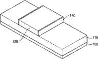
参考图1,可以提供基板100。基板100可以包括:诸如硅基板、锗基板、硅-锗基板等的半导体基板;外延基板;或者诸如玻璃基板的绝缘基板。基板100可以包括其上的各种装置,如晶体管、接触插塞、位线、电容器、金属配线等。Referring to FIG. 1 , a
绝缘层110可以形成在基板100上。绝缘层110可以采用氧化硅、氮化硅、氮氧化硅、铟锡氧化物(ITO)、氧化铝等形成。氧化硅可以包括硼磷硅玻璃(BPSG)、磷硅玻璃(PSG)、非掺杂硅玻璃(USG)、旋涂玻璃(SOG)、等离子增强正硅酸乙酯(plasma-enhanced tetraethyl-orthosilicate,PE-TEOS)等。An insulating
金属结构120可以形成在绝缘层110上。金属结构120可以包括金属层图案或金属氮化物层图案,CNT可以从其表面生长。金属(氮化物)层图案可以包括镍、钴、铁、钛、氮化钛等。它们可以单一使用或结合使用。金属(氮化物)层图案可以采用上述材料通过沉积工艺形成。盖层(未示出)还可以形成在金属(氮化物)层图案上。A
参考图2,催化剂金属层可以形成在绝缘层110上以覆盖金属结构120。催化剂金属层可以包括催化剂材料,如镍、钴、铁等。催化剂材料层可以被退火以具有纳米粒子,如纳米点。催化剂金属层可以被蚀刻,直到可以暴露金属结构120的顶表面,由此在金属结构120的侧壁上形成催化剂间隔物140。Referring to FIG. 2 , a catalytic metal layer may be formed on the insulating
参考图3,多个CNT 150可以形成在催化剂间隔物140的侧壁表面上。CNT 150可以采用包括碳氢化合物的源气体形成。源气体可以通过气化例如甲烷、乙炔、一氧化碳、苯、乙烯等形成。CNT 150可以通过催化热还原工艺、化学气相沉积(CVD)工艺、热化学气相沉积工艺、等离子增强化学气相沉积(PE-CVD)工艺、热丝气相沉积工艺等形成。CNT 150可以由催化剂生长,并且包括在催化剂间隔物140中的催化剂材料的性能可以取决于与催化剂间隔物140接触的层的特性。从而,催化剂间隔物140可以选择性生长CNT 150。Referring to FIG. 3 , a plurality of CNTs 150 may be formed on sidewall surfaces of the
CNT 150可以生长在催化剂间隔物140的侧壁表面上,并且所示生长的CNT 150可以不延伸在平行于绝缘层110或基板100的顶表面的方向上,而是每个CNT 150的端部可以向上弯曲,如图3所示。The CNTs 150 may be grown on the sidewall surfaces of the catalyst spacers 140, and the CNTs 150 grown as shown may not extend in a direction parallel to the top surface of the insulating
参考图4,其上具有弯曲CNT 150的基板100可以旋转。从而,可以给CNT 150施加拉力和压力。拉力可以由基板100的旋转力产生,而向下压CNT 150的压力,可以在基板100旋转时由基板100上的结构例如金属结构120产生。在示范性实施例中,基板100可以旋转的速度为约3,000至约5,000rpm,优选约3,500至约4,500rpm。Referring to FIG. 4, a
挥发性有机溶剂可以提供在绝缘层110的顶表面上。挥发性有机溶剂可以包括丙酮、二甲苯、诸如异丙醇的挥发性醇等。挥发性有机溶剂可以提供到绝缘层110的顶表面中心,并且可以由离心力旋涂在其整个表面上。从而,CNT 150可以由挥发性有机溶剂变湿,并且吸收到绝缘层110的顶表面上。挥发性有机溶剂可以给CNT 150施加粘合力。A volatile organic solvent may be provided on the top surface of the insulating
弯曲的CNT 150可以由上述三种力改变成水平CNT151,使其在平行于绝缘层110或基板100的顶表面的方向上延伸。水平CNT151可以靠近绝缘层110的顶表面,并且在平行于绝缘层110或基板100的顶表面的方向上延伸。The curved CNT 150 may be changed into a
图5至9是图解根据另一个示范性实施例形成CNT的方法的截面图。5 to 9 are cross-sectional views illustrating a method of forming CNTs according to another exemplary embodiment.
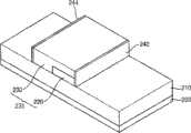
参考图5,可以提供基板200。基板200可以包括:诸如硅基板、锗基板、硅-锗基板等的半导体基板;外延基板;或诸如玻璃基板的绝缘基板。基板200可以包括其上的各种装置,如晶体管、接触插塞、位线、电容器、金属配线等。Referring to FIG. 5 , a
绝缘层210可以形成在基板200上。绝缘层210可以采用氧化硅、氮化硅、氮氧化硅、铟锡氧化物(ITO)、氧化铝等形成。氧化硅可以包括硼磷硅玻璃(BPSG)、磷硅玻璃(PSG)、非掺杂硅玻璃(USG)、旋涂玻璃(SOG)、等离子增强正硅酸乙酯(PE-TEOS)等。An insulating
第一金属层图案220可以形成在绝缘层210上。第一金属层图案220可以包括第一金属,如镍、钴、铁、钛等。它们可以单独使用或结合使用。作为选择,第一金属层图案220可以包括金属氮化物,如氮化钛。第一金属层图案可以采用上述材料通过执行沉积工艺而形成,以形成第一金属层,并且图案化该第一金属层。The first
参考图6,第二金属层可以形成在绝缘层210上,以覆盖第一金属层图案220。第二金属层可以包括防止CNT从第二金属层表面生长的第二金属。第二金属可以包括钯、铂、钨、铌、钒、钼等。它们可以单独使用或结合使用。第二金属层可以通过沉积工艺形成。Referring to FIG. 6 , a second metal layer may be formed on the insulating
第二金属层可以通过光刻工艺图案化,从而可以暴露第一金属层图案220的侧表面A。因此,可以形成除了侧表面A外围绕第一金属层图案220的第二金属层图案230。The second metal layer may be patterned through a photolithography process so that the side surface A of the first
第一和第二金属层图案220和230可以称为金属结构235。The first and second
参考图7,催化剂金属层可以形成在绝缘层210上以覆盖金属结构235。催化剂金属层可以包括催化剂材料,如镍、钴、铁等。催化剂材料层可以被退火,以具有纳米粒子,如纳米点。催化剂金属层可以被蚀刻,直到可以暴露金属结构235的顶表面,由此在金属结构235的侧壁上形成第一和第二催化剂间隔物242和244。第一催化剂间隔物242可以形成在金属结构235的侧壁上,以接触第一金属层图案220的侧表面A,并且第二催化剂间隔物244可以形成在金属结构235的侧壁上,以与第一金属层图案220隔开。Referring to FIG. 7 , a catalyst metal layer may be formed on the insulating
参考图8,多个CNT 250可以形成在第一催化剂间隔物242的侧表面上,并且可以不形成在第二催化剂间隔物244的侧表面上。CNT 250可以由催化剂生长,并且包括在催化剂间隔物242和244中的催化剂材料的性能可以取决于分别接触催化剂间隔物242和244的第一和第二金属层图案220和230的特性。从而,只有第一催化剂间隔物242可以生长CNT 250。CNT 250可以采用包括碳氢化合物的源气体形成。源气体可以通过气化例如甲烷、乙炔、一氧化碳、苯、乙烯等形成。CNT 250可以通过催化热还原工艺、CVD工艺、热化学气相沉积工艺、PE-CVD工艺、热丝气相沉积工艺等形成。Referring to FIG. 8 , a plurality of
CNT 250可以仅生长在第一催化剂间隔物242的侧表面上,并且所示生长的CNT 250可以不延伸在平行于绝缘层210的顶表面的方向上,而是每个CNT 250的端部可以向上弯曲,如图8所示。The
参考图9,其上包括弯曲CNT 250的基板200可以旋转。从而,可以给CNT 250施加拉力和压力。拉力可以由基板200的旋转力产生,而向下压CNT 250的压力可以在基板200旋转时由基板100上面的结构(例如金属结构235)产生。在示范性实施例中,基板200可以旋转的速度为约3000至约5000rpm,优选约3500至约4500rpm。Referring to FIG. 9, a
挥发性有机溶剂可以提供在绝缘层210的顶表面上。挥发性有机溶剂可以包括丙酮、二甲苯、诸如异丙醇的挥发性醇等。挥发性有机溶剂可以提供到绝缘层210的顶表面中心,并且可以通过离心力旋涂在整个表面上。从而,CNT 250可以由挥发性有机溶剂变湿,并且吸收到绝缘层210的顶表面上。挥发性有机溶剂可以给CNT 250施加粘合力。A volatile organic solvent may be provided on the top surface of the insulating
弯曲的CNT 250可以由上述三种力改变成水平CNT251,使其延伸在平行于绝缘层210或基板200的顶表面的方向上。水平CNT251可以非常靠近绝缘层210的顶表面,并且延伸在平行于绝缘层210或基板200的顶表面的方向上,如图9所示。CNT 251可以在动态随机存取存储器(DRAM)装置、闪存装置、相变存储器(PRAM)装置等中取代金属配线。The
图10是图解包括根据示范性实施例的水平CNT的存储器卡的模块图。FIG. 10 is a block diagram illustrating a memory card including horizontal CNTs according to an exemplary embodiment.
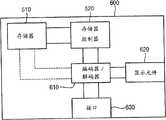
参考图10,存储器卡500可以包括连接到存储器510的存储器控制器520。存储器510可以是具有根据示范性实施例的水平CNT的DRAM或闪存(NAND闪存或NOR闪存)。水平CNT也可以用于存储器控制器520的逻辑电路中的配线。存储器控制器520可以给存储器510提供输入信号以控制存储器510的操作。例如,在存储器卡500中,存储器控制器520可以给存储器510传输主机的指令,以控制输入/输出数据,和/或可以根据所施加的控制信号控制存储器的各种数据。除了简单的存储器卡外,本发明也可以应用于包括类似的存储器和存储器控制器之间可操作关系的其它数字装置。Referring to FIG. 10 , the
图11是图解包括根据示范性实施例的水平CNT的便携式装置的框图。FIG. 11 is a block diagram illustrating a portable device including horizontal CNTs according to an exemplary embodiment.
参考图11,便携式装置600可以包括MP3播放器、视频播放器或便携式多介质播放器(PMP)。便携式装置600可以包括具有根据示范性实施例的水平CNT的存储器510和如上所述的存储器控制器620。存储器510可以是包括水平CNT的DRAM或闪存。Referring to FIG. 11, the
便携式装置600可以包括编码器/解码器(EDC)610、显示元件620和接口630。如图11的虚线所示,数据可以直接从EDC610输入到存储器510,或者直接从存储器510输出到EDC610。The
EDC 610可以编码数据以存储在存储器510中。例如,EDC 610可以执行编码,以将音频数据和/或视频数据存储在MP3播放器或PMP播放器的存储器510中。此外,EDC 610可以执行MPEG编码,以存储视频数据在存储器510中。EDC 610可以包括多个编码器以根据不同种类的数据的形式进行编码。例如,EDC 610可以包括用于编码音频数据的MP3编码器和用于编码视频数据的MPEG编码器。
EDC 610也可以解码从存储器510输出的数据。例如,EDC 610可以解码来自存储器510的MP3音频数据。此外,EDC 610可以解码来自存储器510的MPEG视频数据。EDC 610可以包括多个解码器,以根据不同类型的数据形式而对其解码。例如,EDC 610可以包括用于音频数据的MP3解码器和用于视频数据的MPEG解码器。
EDC 610可以仅包括解码器。例如,编码的数据可以输入到EDC 610,然后EDC 610可以解码输入的数据,并且将解码的数据传输给存储器控制器520或存储器510。
EDC 610可以接收有待编码的数据或者借助于接口630编码的数据。接口630可以与标准的输入装置兼容,例如,FireWire或USB。就是说,端口630可以包括FireWire端口或USB端口等。数据借助于端口630从存储器510输出。
显示元件620可以将从存储器510输出且由EDC 610解码的数据显示到终端用户。例如,显示元件620可以是音频扬声器或显示屏。
图12是图解包括根据示范性实施例的水平CNT的计算机的框图。FIG. 12 is a block diagram illustrating a computer including a horizontal CNT according to an exemplary embodiment.
参考图12,计算机700可以包括存储器510和连接到存储器510的中央处理单元(CPU)710。存储器510可以是具有根据示范性实施例的水平CNT的DRAM或闪存。该计算机700的示例可以是包括闪存作为其主存储器的便携式计算机。存储器510可以直接地连接到CPU 710,或者由总线间接地连接到CPU 710。计算机700可以具有其它传统的辅助装置(图12中未示出)。Referring to FIG. 12 , a computer 700 may include a
根据各示范性实施例,多个CNT可以从基板上金属结构的侧壁上的催化剂间隔物生长,并且挥发性有机溶剂可以提供到基板上以给CNT以粘合力。从而,CNTs可以延伸在平行于基板顶表面的方向上。According to various exemplary embodiments, a plurality of CNTs may be grown from the catalyst spacers on the sidewalls of the metal structure on the substrate, and a volatile organic solvent may be provided onto the substrate to impart adhesion to the CNTs. Thus, CNTs can extend in a direction parallel to the top surface of the substrate.
如前所述是示范性实施例的示例,而不是对其限制。尽管已经描述了几个示范性实施例,但是本领域的技术人员将理解的是,在不脱离本发明原理的新颖性教导和优点的情况下,示范性实施例可以进行各种修改。因此,所有这样的修改旨在包括在所附权利要求限定的本发明的范围内。在权利要求中,装置加功能的条款旨在覆盖这里描述的执行所述功能的结构以及不仅结构等同而且等同结构的结构。因此,应当理解的是,前面所述是对各示范性实施例的说明,而不应解释为限于所揭示的特定示范性实施例,并且所揭示的示范性实施例以及其它示范性实施例旨在包括在所附的权利要求的范围内。What has been described above is an example of an exemplary embodiment, and not a limitation thereof. Although a few exemplary embodiments have been described, those skilled in the art will appreciate that various modifications are possible in the exemplary embodiments without departing from the novel teachings and advantages of the principles of the invention. Accordingly, all such modifications are intended to be included within the scope of this invention as defined in the appended claims. In the claims, means-plus-function clauses are intended to cover the structures described herein as performing the recited function and not only structural equivalents but also equivalent structures. Therefore, it should be understood that the foregoing description is a description of various exemplary embodiments and should not be construed as limited to the particular exemplary embodiments disclosed, and that the disclosed exemplary embodiments as well as other exemplary embodiments are intended to within the scope of the appended claims.
本申请要求2008年12月1日提交的韩国专利申请No.10-2008-0120365的优先权,因此其全部内容通过引用结合于此。This application claims priority from Korean Patent Application No. 10-2008-0120365 filed on December 1, 2008, the entire contents of which are hereby incorporated by reference.
Claims (20)
Translated fromChineseApplications Claiming Priority (2)
| Application Number | Priority Date | Filing Date | Title |
|---|---|---|---|
| KR120365/08 | 2008-12-01 | ||
| KR20080120365AKR101486750B1 (en) | 2008-12-01 | 2008-12-01 | How to form horizontal carbon nanotubes |
Publications (2)
| Publication Number | Publication Date |
|---|---|
| CN101746717Atrue CN101746717A (en) | 2010-06-23 |
| CN101746717B CN101746717B (en) | 2014-07-02 |
Family
ID=42223062
Family Applications (1)
| Application Number | Title | Priority Date | Filing Date |
|---|---|---|---|
| CN200910246780.7AActiveCN101746717B (en) | 2008-12-01 | 2009-12-01 | Methods of forming carbon nanotubes |
Country Status (3)
| Country | Link |
|---|---|
| US (1) | US8535753B2 (en) |
| KR (1) | KR101486750B1 (en) |
| CN (1) | CN101746717B (en) |
Cited By (8)
| Publication number | Priority date | Publication date | Assignee | Title |
|---|---|---|---|---|
| CN101894773A (en)* | 2009-11-30 | 2010-11-24 | 上海上大瑞沪微系统集成技术有限公司 | Preparation method of carbon nano tube salient points |
| CN103097039A (en)* | 2010-09-14 | 2013-05-08 | 应用奈米结构公司 | Glass substrate with carbon nanotubes and manufacturing method thereof |
| US8815341B2 (en) | 2010-09-22 | 2014-08-26 | Applied Nanostructured Solutions, Llc | Carbon fiber substrates having carbon nanotubes grown thereon and processes for production thereof |
| US8951631B2 (en) | 2007-01-03 | 2015-02-10 | Applied Nanostructured Solutions, Llc | CNT-infused metal fiber materials and process therefor |
| US8951632B2 (en) | 2007-01-03 | 2015-02-10 | Applied Nanostructured Solutions, Llc | CNT-infused carbon fiber materials and process therefor |
| US8969225B2 (en) | 2009-08-03 | 2015-03-03 | Applied Nano Structured Soultions, LLC | Incorporation of nanoparticles in composite fibers |
| US9005755B2 (en) | 2007-01-03 | 2015-04-14 | Applied Nanostructured Solutions, Llc | CNS-infused carbon nanomaterials and process therefor |
| US10138128B2 (en) | 2009-03-03 | 2018-11-27 | Applied Nanostructured Solutions, Llc | System and method for surface treatment and barrier coating of fibers for in situ CNT growth |
Families Citing this family (1)
| Publication number | Priority date | Publication date | Assignee | Title |
|---|---|---|---|---|
| US8789884B1 (en)* | 2013-09-09 | 2014-07-29 | Embe Global LLC | Outdoor chaise lounge with integrated lock-box to secure valuables |
Citations (5)
| Publication number | Priority date | Publication date | Assignee | Title |
|---|---|---|---|---|
| US5452905A (en)* | 1990-08-03 | 1995-09-26 | International Business Machines Corporation | Spinning plate for substrates |
| CN1277147A (en)* | 1999-06-15 | 2000-12-20 | 李铁真 | Low-temperature synthesis of carbon nanometre tube with metal catalytic layer of decomposing carbon source gas |
| KR20020003782A (en)* | 2000-07-04 | 2002-01-15 | 이정욱 | fabrication method of carbon nanotubes |
| US20040099438A1 (en)* | 2002-05-21 | 2004-05-27 | Arthur David J. | Method for patterning carbon nanotube coating and carbon nanotube wiring |
| CN1694208A (en)* | 2004-05-06 | 2005-11-09 | 三星Sdi株式会社 | Method for making carbon nanotube field emission device |
Family Cites Families (6)
| Publication number | Priority date | Publication date | Assignee | Title |
|---|---|---|---|---|
| US5405724A (en)* | 1993-03-08 | 1995-04-11 | Xerox Corporation | Photoconductive imaging members and processes thereof comprising solubilized pigment-lewis acid complexes |
| KR100434272B1 (en) | 2001-06-28 | 2004-06-05 | 엘지전자 주식회사 | Method for developing carbon nanotube horizontally |
| KR100376768B1 (en) | 2000-08-23 | 2003-03-19 | 한국과학기술연구원 | Parallel and selective growth and connection method of carbon nanotubes on the substrates for electronic-spintronic device applications |
| JP2006148063A (en)* | 2004-10-22 | 2006-06-08 | Renesas Technology Corp | Wiring structure, semiconductor device, mram, and manufacturing method of semiconductor device |
| KR100593835B1 (en) | 2004-12-29 | 2006-06-28 | 학교법인고려중앙학원 | Lateral growth method of nanowires by patterning catalyst |
| JP2009271259A (en)* | 2008-05-02 | 2009-11-19 | Fujifilm Corp | Surface treating agent for resist pattern, and method of forming resist pattern using the surface treating agent |
- 2008
- 2008-12-01KRKR20080120365Apatent/KR101486750B1/ennot_activeExpired - Fee Related
- 2009
- 2009-11-25USUS12/625,896patent/US8535753B2/ennot_activeExpired - Fee Related
- 2009-12-01CNCN200910246780.7Apatent/CN101746717B/enactiveActive
Patent Citations (5)
| Publication number | Priority date | Publication date | Assignee | Title |
|---|---|---|---|---|
| US5452905A (en)* | 1990-08-03 | 1995-09-26 | International Business Machines Corporation | Spinning plate for substrates |
| CN1277147A (en)* | 1999-06-15 | 2000-12-20 | 李铁真 | Low-temperature synthesis of carbon nanometre tube with metal catalytic layer of decomposing carbon source gas |
| KR20020003782A (en)* | 2000-07-04 | 2002-01-15 | 이정욱 | fabrication method of carbon nanotubes |
| US20040099438A1 (en)* | 2002-05-21 | 2004-05-27 | Arthur David J. | Method for patterning carbon nanotube coating and carbon nanotube wiring |
| CN1694208A (en)* | 2004-05-06 | 2005-11-09 | 三星Sdi株式会社 | Method for making carbon nanotube field emission device |
Cited By (12)
| Publication number | Priority date | Publication date | Assignee | Title |
|---|---|---|---|---|
| US8951631B2 (en) | 2007-01-03 | 2015-02-10 | Applied Nanostructured Solutions, Llc | CNT-infused metal fiber materials and process therefor |
| US8951632B2 (en) | 2007-01-03 | 2015-02-10 | Applied Nanostructured Solutions, Llc | CNT-infused carbon fiber materials and process therefor |
| US9005755B2 (en) | 2007-01-03 | 2015-04-14 | Applied Nanostructured Solutions, Llc | CNS-infused carbon nanomaterials and process therefor |
| US9573812B2 (en) | 2007-01-03 | 2017-02-21 | Applied Nanostructured Solutions, Llc | CNT-infused metal fiber materials and process therefor |
| US9574300B2 (en) | 2007-01-03 | 2017-02-21 | Applied Nanostructured Solutions, Llc | CNT-infused carbon fiber materials and process therefor |
| US10138128B2 (en) | 2009-03-03 | 2018-11-27 | Applied Nanostructured Solutions, Llc | System and method for surface treatment and barrier coating of fibers for in situ CNT growth |
| US8969225B2 (en) | 2009-08-03 | 2015-03-03 | Applied Nano Structured Soultions, LLC | Incorporation of nanoparticles in composite fibers |
| CN101894773A (en)* | 2009-11-30 | 2010-11-24 | 上海上大瑞沪微系统集成技术有限公司 | Preparation method of carbon nano tube salient points |
| CN101894773B (en)* | 2009-11-30 | 2011-10-26 | 上海上大瑞沪微系统集成技术有限公司 | Preparation method of carbon nano tube salient points |
| CN103097039A (en)* | 2010-09-14 | 2013-05-08 | 应用奈米结构公司 | Glass substrate with carbon nanotubes and manufacturing method thereof |
| US8784937B2 (en) | 2010-09-14 | 2014-07-22 | Applied Nanostructured Solutions, Llc | Glass substrates having carbon nanotubes grown thereon and methods for production thereof |
| US8815341B2 (en) | 2010-09-22 | 2014-08-26 | Applied Nanostructured Solutions, Llc | Carbon fiber substrates having carbon nanotubes grown thereon and processes for production thereof |
Also Published As
| Publication number | Publication date |
|---|---|
| US20100136226A1 (en) | 2010-06-03 |
| US8535753B2 (en) | 2013-09-17 |
| CN101746717B (en) | 2014-07-02 |
| KR20100061979A (en) | 2010-06-10 |
| KR101486750B1 (en) | 2015-01-28 |
Similar Documents
| Publication | Publication Date | Title |
|---|---|---|
| CN101746717A (en) | methods of forming carbon nanotubes | |
| US8039919B2 (en) | Memory devices having a carbon nanotube | |
| JP6356396B2 (en) | Semiconductor device and manufacturing method thereof | |
| TWI703633B (en) | Electronic device and methods to manufacture electronic device, to provide maskless air gap flow, and to provide replacement interlayer dielectric flow | |
| US10867923B2 (en) | Semiconductor device | |
| US8058183B2 (en) | Restoring low dielectric constant film properties | |
| US10937689B2 (en) | Self-aligned hard masks with converted liners | |
| US9911644B2 (en) | Semiconductor devices and methods of fabricating the same | |
| US20100081286A1 (en) | Method of etching carbon-containing layer, method of forming contact hole using the same, and method of manufacturing semiconductor device using the same | |
| US20070235847A1 (en) | Method of making a substrate having thermally conductive structures and resulting devices | |
| CN102386064A (en) | Manufacturing method of metal-oxide-metal capacitor | |
| CN102394215A (en) | Manufacturing method of multilayer metal-silicon oxide-metal capacitor | |
| US20110318914A1 (en) | Method of fabricating semiconductor device | |
| US7877865B2 (en) | Method of forming a wiring having carbon nanotube | |
| US20090246949A1 (en) | Methods of manufacturing semiconductor devices | |
| US20120146227A1 (en) | Integrated circuit nanowires | |
| US9240552B2 (en) | Carbon nanotube semiconductor devices and deterministic nanofabrication methods | |
| CN102760687A (en) | Semiconductor device with air space and manufacture method thereof | |
| KR20120033643A (en) | Method of manufacturing low-k porous dielectric film and method of manufacturing semiconductor device using the same | |
| CN102558266B (en) | Template derivative for forming ultra-low dielectric layer and method of forming ultra-low dielectric layer using same | |
| CN101225193B (en) | Template derivative for forming ultra-low dielectric layer and method for forming ultra-low dielectric layer | |
| CN102437024B (en) | Method for manufacturing multilayer metal-silicon oxide-metal (MOM) capacitor | |
| US7843070B2 (en) | Nanotube and metal composite interconnects | |
| TWI848270B (en) | Graphene barrier for electrical interconnects and producing method thereof | |
| CN100334696C (en) | Etching process for silicide low dielectric material |
Legal Events
| Date | Code | Title | Description |
|---|---|---|---|
| C06 | Publication | ||
| PB01 | Publication | ||
| C10 | Entry into substantive examination | ||
| SE01 | Entry into force of request for substantive examination | ||
| C14 | Grant of patent or utility model | ||
| GR01 | Patent grant |