CN101742316B - NIOS II-based video processing method - Google Patents
NIOS II-based video processing methodDownload PDFInfo
- Publication number
- CN101742316B CN101742316BCN 200910254404CN200910254404ACN101742316BCN 101742316 BCN101742316 BCN 101742316BCN 200910254404CN200910254404CN 200910254404CN 200910254404 ACN200910254404 ACN 200910254404ACN 101742316 BCN101742316 BCN 101742316B
- Authority
- CN
- China
- Prior art keywords
- para
- signal
- ctrl1
- point
- interpolation result
- Prior art date
- Legal status (The legal status is an assumption and is not a legal conclusion. Google has not performed a legal analysis and makes no representation as to the accuracy of the status listed.)
- Expired - Fee Related
Links
- 238000003672processing methodMethods0.000titleclaimsabstractdescription7
- 238000000034methodMethods0.000claimsabstractdescription54
- 238000006243chemical reactionMethods0.000claimsabstractdescription23
- 230000001360synchronised effectEffects0.000claimsdescription61
- 239000011159matrix materialSubstances0.000claimsdescription41
- 238000012545processingMethods0.000claimsdescription38
- 230000000750progressive effectEffects0.000claimsdescription17
- 238000004364calculation methodMethods0.000claimsdescription15
- 238000013461designMethods0.000claimsdescription11
- 101100311460Schizosaccharomyces pombe (strain 972 / ATCC 24843) sum2 geneProteins0.000claimsdescription9
- 238000010606normalizationMethods0.000claimsdescription4
- 230000003044adaptive effectEffects0.000claimsdescription3
- 238000012544monitoring processMethods0.000abstractdescription9
- 238000005516engineering processMethods0.000abstractdescription2
- 230000005540biological transmissionEffects0.000description62
- 238000010586diagramMethods0.000description36
- 230000006870functionEffects0.000description17
- 238000012546transferMethods0.000description12
- 238000013500data storageMethods0.000description6
- 238000004891communicationMethods0.000description5
- 230000008569processEffects0.000description5
- 101000885321Homo sapiens Serine/threonine-protein kinase DCLK1Proteins0.000description4
- 102100039758Serine/threonine-protein kinase DCLK1Human genes0.000description4
- 238000004088simulationMethods0.000description4
- 230000003068static effectEffects0.000description3
- 230000008859changeEffects0.000description2
- 239000002131composite materialSubstances0.000description2
- 230000002093peripheral effectEffects0.000description2
- 230000004044responseEffects0.000description2
- ATHVAWFAEPLPPQ-VRDBWYNSSA-N1-stearoyl-2-oleoyl-sn-glycero-3-phosphocholineChemical compoundCCCCCCCCCCCCCCCCCC(=O)OC[C@H](COP([O-])(=O)OCC[N+](C)(C)C)OC(=O)CCCCCCC\C=C/CCCCCCCCATHVAWFAEPLPPQ-VRDBWYNSSA-N0.000description1
- 241001504505Troglodytes troglodytesSpecies0.000description1
- 230000000694effectsEffects0.000description1
- 238000001914filtrationMethods0.000description1
- 230000006872improvementEffects0.000description1
- 230000010365information processingEffects0.000description1
- 230000010354integrationEffects0.000description1
- 238000005457optimizationMethods0.000description1
- 230000009467reductionEffects0.000description1
- 238000005070samplingMethods0.000description1
- 239000007787solidSubstances0.000description1
- 238000001228spectrumMethods0.000description1
- 230000009466transformationEffects0.000description1
- 239000011800void materialSubstances0.000description1
Images


Landscapes
- Image Processing (AREA)
Abstract
Translated fromChinese
Description
Translated fromChinese技术领域technical field
本发明属于嵌入式视频监视技术领域,具体涉及一种基于NIOS II的视频处理方法。The invention belongs to the technical field of embedded video surveillance, in particular to a video processing method based on NIOS II.
背景技术Background technique
视频监视近年来得到了迅速的发展,应用范围不断地扩展。以往国内使用的视频监视系统主要是模拟系统,到了20世纪90年代末,随着网络宽带、计算机处理能力和存储容量的迅速提高,以及各种实用视频信息处理技术的出现,视频监视从模拟视频监视进入了数字化的网络时代,即数字视频监视系统。数字视频监视系统将摄像机获得的模拟信号转变成数字信号,便于计算机处理.在计算机显示器上显示或者在监视器上显示实时活动图像的同时,还可以将视频信号存储于计算机的硬盘内,或者在网络上进行传输。Video surveillance has developed rapidly in recent years, and the scope of application is constantly expanding. In the past, the video surveillance system used in China was mainly an analog system. By the end of the 1990s, with the rapid improvement of network broadband, computer processing power and storage capacity, and the emergence of various practical video information processing technologies, video surveillance has evolved from analog video Surveillance has entered the digital network era, that is, digital video surveillance system. The digital video surveillance system converts the analog signal obtained by the camera into a digital signal, which is convenient for computer processing. While displaying real-time moving images on the computer monitor or on the monitor, the video signal can also be stored in the hard disk of the computer, or in the transmission over the network.
传统的视频监视的嵌入式设计架构是应用MCU+ASIC来实现系统硬件基础,由操作系统调度不同的任务实现系统的运行。但系统硬件的可裁剪性较差,系统优化、升级不是很方便。The embedded design architecture of traditional video surveillance uses MCU+ASIC to realize the hardware foundation of the system, and the operating system schedules different tasks to realize the operation of the system. However, the tailorability of system hardware is poor, and system optimization and upgrade are not very convenient.
传统的视频监视方法中的MCU为系统总控制中枢,一般可用高档单片机或ARM.其它功能模块可以用专用的芯片来实现。CVBS模拟视频信号经过视频的模数转换芯片输出数字视频信号,MCU控制整个系统的运行,数字视频信号经过数字视频处理芯片,输出需要的视频信号,经过压缩存储(可选),最后传输到显示终端。因此,传统的视频监视的硬件需要用多个元件来实现,集成度不高,且系统成本较高,系统单板一旦做成,系统更改、升级比较困难。The MCU in the traditional video monitoring method is the overall control center of the system, and generally high-end single-chip microcomputer or ARM can be used. Other functional modules can be realized by dedicated chips. The CVBS analog video signal outputs the digital video signal through the analog-to-digital conversion chip of the video, and the MCU controls the operation of the entire system. The digital video signal passes through the digital video processing chip, outputs the required video signal, and is compressed and stored (optional), and finally transmitted to the display terminal. Therefore, traditional video surveillance hardware needs to be implemented with multiple components, the integration level is not high, and the system cost is high. Once the system single board is completed, it is difficult to change and upgrade the system.
现有的基于NIOS II软核的视频监视方法,实现了视频处理和NIOS II系统的结合。CVBS模拟视频信号经过模数转换芯片输出数字视频信号,数字视频信号经过视频采集处理模块和NIOS II系统控制协同工作,最后输出视频信号传输到显示终端。但现有的NIOS II软核的视频监视方法仅局限于视频的简单处理,实时监控,不能同时满足视频监视的实时监视、采集、存储和传输的要求,也没有充分发挥出基于NIOS II软核的特色。The existing video surveillance method based on NIOS II soft core realizes the combination of video processing and NIOS II system. The CVBS analog video signal outputs a digital video signal through the analog-to-digital conversion chip, and the digital video signal is controlled and coordinated by the video acquisition and processing module and the NIOS II system, and finally the output video signal is transmitted to the display terminal. But the video monitoring method of existing NIOS II soft core is only limited to the simple processing of video, real-time monitoring, can not satisfy the requirement of real-time monitoring, collection, storage and transmission of video monitoring simultaneously, also does not bring into full play based on NIOS II soft core features.
现有的视频处理的视频缩放大多采用线性插值方法,方法简单,但由于线性插值平坦的通带过窄,对图像高频部分有很大衰减,若要得到较好的插值结果,又需要高阶滤波函数来实现,这无疑增加了计算复杂度、具体实现困难较大。Most of the video scaling in existing video processing adopts linear interpolation method, which is simple, but because the flat passband of linear interpolation is too narrow, it will greatly attenuate the high-frequency part of the image. To obtain better interpolation results, high This will undoubtedly increase the computational complexity and make it more difficult to implement.
发明内容Contents of the invention
本发明目的在于提供一种基于NIOS II的视频处理方法,解决了现有的视频处理的方法未能充分利用NIOS II软核,且方法单一的技术问题。The object of the invention is to provide a kind of video processing method based on NIOS II, solve the method for existing video processing and fail to fully utilize NIOS II soft core, and the technical problem of method singleness.
本发明针对上述技术问题的技术解决方案如下:The technical solutions of the present invention for the above-mentioned technical problems are as follows:
一种基于NIOS II的视频处理方法,其特殊之处在于,该方法包括以下步骤:A kind of video processing method based on NIOS II, its special feature is that the method comprises the following steps:
[1.1]解码:将BT656视频信号通过BT656解码解码为隔行的YCbCr数字视频信号及隔行的同步信号I;[1.1] Decoding: BT656 video signal is decoded into interlaced YCbCr digital video signal and interlaced synchronous signal I through BT656 decoding;
[1.2]去隔行:将隔行的YCbCr数字视频信号及隔行的同步信号I通过去隔行转换为逐行的YCbCr数字视频信号及逐行的同步信号I;[1.2] Deinterlacing: convert the interlaced YCbCr digital video signal and interlaced synchronous signal I into progressive YCbCr digital video signal and progressive synchronous signal I through deinterlacing;
[1.3]视频缩放:将逐行的YCbCr数字视频信号以及逐行的同步信号I通过视频缩放至YCbCr转RGB,转换为RGB数字视频信号;[1.3] Video scaling: the progressive YCbCr digital video signal and the progressive synchronous signal I are converted to RGB digital video signal through video scaling to YCbCr to RGB;
[1.4]时序调配:将RGB数字视频信号以及NIOS II配置时钟信号通过VGA时序发生消隐调配为RGB数字视频信号、同步信号II以及供VGA显示的时钟信号;[1.4] Timing allocation: RGB digital video signal and NIOS II configuration clock signal are blanked and allocated to RGB digital video signal, synchronous signal II and clock signal for VGA display through VGA timing;
[1.5]视频缩放:根据VGA时序发生输出的同步信号II、NIOS II控制系统提供的配置缩放参数、去隔行输出的同步信号I,将去隔行输出的逐行的YCbCr数字视频信号通过视频缩放缩放为YCbCr数字视频信号;[1.5] Video scaling: According to the synchronous signal II output by VGA timing, the configuration scaling parameters provided by the NIOS II control system, and the synchronous signal I output by deinterlacing, the progressive YCbCr digital video signal output by deinterlacing is scaled by video scaling It is a YCbCr digital video signal;
[1.6]数字视频信号格式转换:将缩放的YCbCr数字视频信号通过YCbCr转RGB转换为RGB数字视频信号;[1.6] Digital video signal format conversion: convert the scaled YCbCr digital video signal to RGB digital video signal through YCbCr to RGB;
[1.7]时序调配:RGB数字视频信号以及NIOS II配置时钟信号通过VGA时序发生输出RGB数字视频信号、VGA同步信号II以及供VGA显示的时钟信号;将RGB数字视频信号、同步信号II以及供VGA显示的时钟信号一路输至MUX选择,另一路经NIOS II控制系统22输至MUX选择;[1.7] Timing deployment: RGB digital video signal and NIOS II configuration clock signal generate and output RGB digital video signal, VGA synchronous signal II and clock signal for VGA display through VGA timing; combine RGB digital video signal, synchronous signal II and clock signal for VGA The displayed clock signal is output to the MUX selection one way, and the other is output to the MUX selection through the NIOS II
[1.8]信号选择:VGA时序发生输出的RGB数字视频信号、VGA同步信号II以及供VGA显示的时钟信号直接经MUX选择输出供VGA显示,或VGA时序发生输出的RGB数字视频信号、VGA同步信号II以及供VGA显示的时钟信号经NIOS II控制系统控制后再经MUX选择输出供VGA显示。[1.8] Signal selection: RGB digital video signal output by VGA timing generation, VGA synchronous signal II and clock signal for VGA display are directly selected and output by MUX for VGA display, or RGB digital video signal and VGA synchronous signal output by VGA timing generation II and the clock signal for VGA display are controlled by NIOS II control system and then selected and output by MUX for VGA display.
以上所述的步骤[1.5]具体的实现方法为:The specific implementation method of the above-mentioned step [1.5] is as follows:
1)计算插值步长1) Calculate the interpolation step size
视频缩放(213)根据输入的同步信号I和同步信号II计算插值步长,即计算:插值步长=同步信号I/同步信号II得插值步长;Video scaling (213) calculates the interpolation step-length according to the synchronous signal I of input and synchronous signal II, promptly calculates: interpolation step-length=the interpolation step-length of synchronous signal I/synchronous signal II;
1.1)确定新像素点X插值的位置1.1) Determine the position of the new pixel point X interpolation
根据插值步长来确定新像素点X插值位置;Determine the X interpolation position of the new pixel point according to the interpolation step;
2)计算当前像素点X的非线性插值结果x_lans2) Calculate the nonlinear interpolation result x_lans of the current pixel point X
以2n个原始像素点为方阵式区域,形成X1~X2n个像素点,得到X位置的像素值即非线性插值结果x_lans,其中n取≥4的偶数;Use 2n original pixels as a square matrix area to form X1~X2n pixels, and get the pixel value at X position, which is the nonlinear interpolation result x_lans, where n is an even number ≥ 4;
3)确定当前像素点的线性插值结果x_bi;3) Determine the linear interpolation result x_bi of the current pixel;
4)通过自适应判断确定最终插值结果。4) Determine the final interpolation result through adaptive judgment.
以上所述的步骤2)的具体实现方法是:The concrete realization method of above-mentioned step 2) is:
2.1)计算方阵的列缩放系数para_v、方阵的行缩放系数para_h、2.1) Calculate the column scaling factor para_v of the square matrix, the row scaling factor para_h of the square matrix,
应用Lanczos非线性插值函数,Applying the Lanczos nonlinear interpolation function,
来确定方阵的列缩放系数para_v以及方阵 To determine the column scaling factor para_v of the square matrix and the square matrix
的行缩放系数para_h;The row scaling factor para_h;
2.2)确定查找表2.2) Determine the lookup table
将步骤2.1)所得的方阵的列缩放系数para_v、方阵的行缩放系数para_h写入查找表;The column scaling factor para_v of the square matrix of step 2.1) gained, the row scaling factor para_h of square matrix are written into look-up table;
2.3)确定每列的垂直向系数2.3) Determine the vertical coefficient of each column
查找步骤2.2)中所得查找表的方阵的列缩放系数para_v,计算归一化的系数的和sum1以及每列的垂直向系数;Find the column scaling coefficient para_v of the square matrix of gained look-up table in step 2.2), calculate the coefficient sum sum1 of normalization and the vertical direction coefficient of each column;
归一化的系数的和sum1为方阵的列缩放系数para_v之和;The sum of the normalized coefficients sum1 is the sum of the column scaling coefficients para_v of the square matrix;
计算:垂直向系数X_m1=(X1*para_v1+X5*para_v2+X9*para_v3+X13*para_v4)/sum1Calculation: Vertical coefficient X_m1=(X1*para_v1+X5*para_v2+X9*para_v3+X13*para_v4)/sum1
垂直向系数X_m2=(X2*para_v1+X6*para_v2+X10*para_v3+X14*para_v4)/sum1Vertical coefficient X_m2=(X2*para_v1+X6*para_v2+X10*para_v3+X14*para_v4)/sum1
垂直向系数X_m3=(X3*para_v1+X7*para_v2+X11*para_v3+X15*para_v4)/sum1Vertical coefficient X_m3=(X3*para_v1+X7*para_v2+X11*para_v3+X15*para_v4)/sum1
垂直向系数X_m4=(X4*para_v1+X8*para_v2+X12*para_v3+X16*para_v4)/sum1Vertical coefficient X_m4=(X4*para_v1+X8*para_v2+X12*para_v3+X16*para_v4)/sum1
则得每列的垂直向系数;Then get the vertical coefficient of each column;
2.4)确定最终X位置的非线性插值结果X_lans2.4) Determine the nonlinear interpolation result X_lans of the final X position
查找步骤2.2)中所得查找表的方阵的行缩放系数para_h计算水平向归一化的系数的和sum2;The row scaling factor para_h of the square matrix of gained look-up table in the search step 2.2) calculates the sum sum2 of the coefficient of horizontal normalization;
水平向归一化的系数的和sum2为方阵的行缩放系数para_h之和;The sum of the horizontally normalized coefficients sum2 is the sum of the row scaling coefficients para_h of the square matrix;
计算:X_lans=(X_m1*para_h1+X_m2*para_h2+X_m3*para_h3+…)/sum2,得非线性插值结果X_lans;Calculation: X_lans=(X_m1*para_h1+X_m2*para_h2+X_m3*para_h3+…)/sum2, get the nonlinear interpolation result X_lans;
2.5)过冲和下冲控制2.5) Overshoot and undershoot control
2.5.1)选取方阵相邻列的原始像素点位置的最大值XL_max以及方阵相邻列的原始像素点位置的最小值XL_min;2.5.1) Select the maximum value XL_max of the original pixel position of the adjacent column of the square array and the minimum value XL_min of the original pixel position of the adjacent column of the square array;
2.5.2)根据设计要求选择n位过冲控制门限0T_ctrl和n位下冲控制门限UT_ctrl,其范围是0~2n-1;2.5.2) Select the n-bit overshoot control threshold 0T_ctrl and the n-bit undershoot control threshold UT_ctrl according to the design requirements, and the range is 0~2n -1;
2.5.3)判定过冲和下冲控制以确定非线性插值结果X_lans1;2.5.3) Determine the overshoot and undershoot control to determine the nonlinear interpolation result X_lans1;
2.5.3.1)将经步骤2.4)所得的非线性插值结果X_lans与原始像素点位置的最大值XL_max进行比较后,控制过冲,确定非线性插值结果X_lans1;2.5.3.1) After comparing the nonlinear interpolation result X_lans obtained in step 2.4) with the maximum value XL_max of the original pixel position, control the overshoot and determine the nonlinear interpolation result X_lans1;
2.5.3.2)将经步骤2.4)所得的非线性插值结果X_lans与原始像素点位置的最小值X_min进行比较后,进行下冲控制,确定非线性插值结果X_lans1。2.5.3.2) After comparing the nonlinear interpolation result X_lans obtained in step 2.4) with the minimum value X_min of the original pixel position, perform undershoot control to determine the nonlinear interpolation result X_lans1.
以上所述的步骤3)的具体实现方法是:The concrete realization method of above-mentioned step 3) is:
3.1)确定待插值的水平左右点3.1) Determine the horizontal left and right points to be interpolated
计算:calculate:
待插值的水平左点LL1=[X1*N_ctrl1+X2*(2n-N_ctrl1)]/2nHorizontal left point LL1 to be interpolated = [X1*N_ctrl1+X2*(2n -N_ctrl1)]/2n
待插值的水平右点LR1=[X4*N_ctrl1+X3*(2n-N_ctrl1)]/2nHorizontal right point LR1 to be interpolated = [X4*N_ctrl1+X3*(2n -N_ctrl1)]/2n
待插值的水平左点LL2=[X5*N_ctrl1+X6*(2n-N_ctrl1)]/2nHorizontal left point LL2 to be interpolated = [X5*N_ctrl1+X6*(2n -N_ctrl1)]/2n
待插值的水平右点LR2=[X8*N_ctrl1+X7*(2n-N_ctrl1)]/2nHorizontal right point to be interpolated LR2=[X8*N_ctrl1+X7*(2n -N_ctrl1)]/2n
待插值的水平左点LL3=[X9*N_ctrl1+X10*(2n-N_ctrl1)]/2nHorizontal left point LL3 to be interpolated = [X9*N_ctrl1+X10*(2n -N_ctrl1)]/2n
待插值的水平右点LR3=[X12*N_ctrl1+X11*(2n-N_ctrl1)]/2nHorizontal right point LR3 to be interpolated=[X12*N_ctrl1+X11*(2n -N_ctrl1)]/2n
待插值的水平左点LL4=[X13*N_ctrl1+X14*(2n-N_ctrl1)]/2nHorizontal left point LL4 to be interpolated = [X13*N_ctrl1+X14*(2n -N_ctrl1)]/2n
待插值的水平右点LR4=[X16*N_ctrl1+X15*(2n-N_ctrl1)]/2nHorizontal right point to be interpolated LR4=[X16*N_ctrl1+X15*(2n -N_ctrl1)]/2n
其中n位门限N_ctrl1选取范围为0~2n-1,得待插值的水平左右点;Among them, the selection range of the n-bit threshold N_ctrl1 is 0~2n -1, and the horizontal left and right points to be interpolated are obtained;
3.2)确定线性插值点3.2) Determine the linear interpolation point
计算:calculate:
线性插值点X_l1=LL1*(1-x_offset)+LR1*x_offset,Linear interpolation point X_l1=LL1*(1-x_offset)+LR1*x_offset,
线性插值点X_l2=LL2*(1-x_offset)+LR2*x_offset,Linear interpolation point X_l2=LL2*(1-x_offset)+LR2*x_offset,
线性插值点X_l3=LL3*(1-x_offset)+LR3*x_offset,Linear interpolation point X_l3=LL3*(1-x_offset)+LR3*x_offset,
线性插值点X_l4=LL4*(1-x_offset)+LR4*x_offset,Linear interpolation point X_l4=LL4*(1-x_offset)+LR4*x_offset,
其中x_offset为水平向偏移量,得线性插值点;Among them, x_offset is the horizontal offset, and the linear interpolation point is obtained;
3.3)确定垂直方向的上点X_UP,垂直方向的下点X_DN3.3) Determine the upper point X_UP in the vertical direction and the lower point X_DN in the vertical direction
计算:calculate:
垂直方向的上点X_UP=[X_11*N_ctrl1+X_l2*(2n-N_ctrl1)]/2n,The upper point in the vertical direction X_UP=[X_11*N_ctrl1+X_l2*(2n -N_ctrl1)]/2n ,
垂直方向的下点X_DN=[X_l3*N_ctrl1+X_l4*(2n-N_ctrl1)]/2n,The lower point in the vertical direction X_DN=[X_l3*N_ctrl1+X_l4*(2n -N_ctrl1)]/2n ,
得垂直方向上的点X_UP及垂直方向的下点X_DN;Get the point X_UP in the vertical direction and the down point X_DN in the vertical direction;
3.4)得到线性插值结果X_bi3.4) Get the linear interpolation result X_bi
计算:calculate:
X_bi=X_UP*(1-y_offset)+X_DN*y_offset,其中y_offset为垂直向偏移量,得线性插值结果X_bi;X_bi=X_UP*(1-y_offset)+X_DN*y_offset, where y_offset is the vertical offset, and the linear interpolation result X_bi is obtained;
以上所述的步骤4)的具体实现方法是:The concrete realization method of above-mentioned step 4) is:
将线性插值结果X_bi与非线性插值结果X_lans1进行对比以确定最终插值结果;Compare the linear interpolation result X_bi with the nonlinear interpolation result X_lans1 to determine the final interpolation result;
4.1)选取原2n个像素点的位置的最大值Ymax,选取原2n个像素点的位置的最小值Ymin;4.1) Select the maximum value Ymax of the positions of the original 2n pixels, and select the minimum value Ymin of the positions of the original 2n pixels;
4.2)将原2n个像素点的位置的最大值Ymax与原2n个像素点的位置的最小值Ymin的差值和n位门限N_ctrl2进行比较,确定插值结果;4.2) Compare the difference between the maximum value Ymax of the positions of the original 2n pixels and the minimum value Ymin of the positions of the original 2n pixels with the n-bit threshold N_ctrl2 to determine the interpolation result;
以上所述的步骤2.1)的具体实现方法为:The concrete realization method of above-mentioned step 2.1) is:
计算方阵的列缩放系数para_v=sinc(距X位置的垂直向行数-X)*sinc((距X位置的垂直向行数-X)/a),其中X取0/256~256/256中的任意值,a=n/2,则得方阵的列缩放系数;Calculate the column scaling factor of the square matrix para_v=sinc(number of vertical rows from X position-X)*sinc((number of vertical rows from X position-X)/a), where X takes 0/256~256/ Any value in 256, a=n/2, then get the column scaling factor of square array;
计算方阵的行缩放系数para_h=sinc(距X位置的水平向列数-X)*sinc((距X位置的水平向列数-X)/a),其中X取0/256~256/256中的任意值,a=n/2,则得方阵的行缩放系数。Calculate the row scaling factor of the square matrix para_h=sinc(horizontal nematic number from X position-X)*sinc((horizontal nematic number from X position-X)/a), where X takes 0/256~256/ Any value in 256, a=n/2, then the row scaling factor of the square matrix is obtained.
以上所述的步骤2.5.3.1)的具体实现方法为:The concrete realization method of above-mentioned step 2.5.3.1) is:
2.5.3.1.1)如果X_lans>X_max,则非线性插值结果X_lans1=X_lans-(X_lans-X_max)*0T_ctrl/2n;2.5.3.1.1) If X_lans>X_max, the nonlinear interpolation result X_lans1=X_lans-(X_lans-X_max)*0T_ctrl/2n ;
当X_lans1>255时,则非线性插值结果X_lans1值确定为X_lans1=255;When X_lans1>255, the non-linear interpolation result X_lans1 value is determined as X_lans1=255;
2.5.3.1.2)如果非线性插值结果X_lans<原始像素点位置的最小值X_min,则非线性插值结果X_lans1=X_lans+(X_min-X_lans)*UT_ctrl/2n;当非线性插值结果X_lans1<0时,则非线性插值结果X_lans1值确定为X_lans 1=0。2.5.3.1.2) If the nonlinear interpolation result X_lans<the minimum value X_min of the original pixel position, then the nonlinear interpolation result X_lans1=X_lans+(X_min-X_lans)*UT_ctrl/2n ; when the nonlinear interpolation result X_lans1<0 , then the nonlinear interpolation result X_lans1 value is determined as
以上所述的步骤4.2)的具体实现方法是:若原2n个像素点的位置的最大值Ymax-原2n个像素点的位置的最小值Ymin>n位门限N_ctrl2,则插值结果为线性插值X_bi;若原2n个像素点的位置的最大值Ymax-原2n个像素点的位置的最小值Ymin<n位门限N_ctrl2,则插值结果为非线性插值结果X_lans,其中n位门限N_ctrl2的取值范围为0~2n-1。The specific implementation method of the above-mentioned step 4.2) is: if the maximum value Ymax of the positions of the original 2n pixels-the minimum value Ymin of the positions of the original 2n pixels>n-bit threshold N_ctrl2, then the interpolation result is a linear interpolation X_bi; if the maximum value Ymax of the position of the original 2n pixels-the minimum value Ymin of the position of the original 2n pixels <n-bit threshold N_ctrl2, then the interpolation result is the nonlinear interpolation result X_lans, where the n-bit threshold N_ctrl2 is taken The value range is 0~2n -1.
以上所述的步骤[1.1]中的去隔行(212)采用双口RAM来实现。The de-interlacing (212) in the above-mentioned step [1.1] is implemented by dual-port RAM.
以上所述的步骤[1.6]中的YCbCr转RGB(214)应用矩阵YCbCr to RGB (214) application matrix in the above step [1.6]
本发明的优点如下:The advantages of the present invention are as follows:
1)适用性强,输出不同的VGA制式可通过参数配置;1) Strong applicability, different output VGA formats can be configured through parameters;
2)本发明使用多相位插值方法减少计算的复杂度;2) the present invention uses the polyphase interpolation method to reduce the complexity of calculation;
3)本发明使用插值系数查找表方法易于更新:3) the present invention uses interpolation coefficient look-up table method to be easy to update:
在视频处理的过程中只需要调整查找表的内容,即可实现视频处理中的视频缩放;In the process of video processing, it is only necessary to adjust the content of the lookup table to realize video scaling in video processing;
4)本发明插值精度达到1/256个像素值,使得图像清晰度更高;4) The interpolation precision of the present invention reaches 1/256 pixel value, making the image definition higher;
5)本发明理论上可无限放大视频信号,可将视频信号最小缩至原视频信号的1/2。5) The present invention can theoretically amplify the video signal infinitely, and can minimize the video signal to 1/2 of the original video signal.
附图说明Description of drawings
图1为本发明视频监视系统框图;Fig. 1 is a block diagram of a video surveillance system of the present invention;
图2为本发明视频处理示意框图;Fig. 2 is a schematic block diagram of video processing in the present invention;
图3为本发明视频信号转换输出的BT656行信号时序图;Fig. 3 is the BT656 line signal timing diagram of video signal conversion output of the present invention;
图4为本发明BT656解码接口示意图;Fig. 4 is the BT656 decoding interface schematic diagram of the present invention;
图5为本发明BT656解码接口时序图;Fig. 5 is the sequence diagram of BT656 decoding interface of the present invention;
图6为本发明偶场同步信号1时序图;Fig. 6 is a timing diagram of even
图7为本发明奇场同步信号1时序图;Fig. 7 is a timing diagram of odd field
图8为本发明双口RAM工作监测波形图;Fig. 8 is a dual-port RAM work monitoring waveform diagram of the present invention;
图9为本发明去隔行接口示意图;Fig. 9 is a schematic diagram of the deinterlacing interface of the present invention;
图10为本发明YCbCr输出时序图;Fig. 10 is a timing diagram of YCbCr output in the present invention;
图11为本发明视频缩放接口示意图;Fig. 11 is a schematic diagram of the video scaling interface of the present invention;
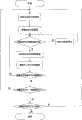
图12为本发明视频缩放的流程示意图;FIG. 12 is a schematic flow chart of video scaling in the present invention;
图13为本发明一实施例计算插值点X的位置示意图;Fig. 13 is a schematic diagram of calculating the position of the interpolation point X according to an embodiment of the present invention;
图14为本发明一实施例示意图;Figure 14 is a schematic diagram of an embodiment of the present invention;
图15为本发明一实施例的非线性插值函数Lanczos公式中a的值的幅频响应示意图;Fig. 15 is a schematic diagram of the amplitude-frequency response of the value of a in the nonlinear interpolation function Lanczos formula of an embodiment of the present invention;
图16为本发明YCrCb转RGB的接口示意图;Fig. 16 is a schematic diagram of the interface of YCrCb to RGB in the present invention;
图17为本发明VGA时序发生接口示意图;Fig. 17 is a schematic diagram of the VGA timing generation interface of the present invention;
图18为本发明行同步信号IIVGA时序图;FIG. 18 is a timing diagram of the line synchronization signal IIVGA of the present invention;
图19为本发明场同步信号IIVGA时序图;FIG. 19 is a timing diagram of the field synchronization signal IIVGA of the present invention;
图20为本发明NIOSII控制系统结构示意图;Fig. 20 is the structural representation of NIOSII control system of the present invention;
图21为本发明NIOSII硬件连接图;Fig. 21 is a NIOSII hardware connection diagram of the present invention;
图22为本发明SDRAM控制核结构示意图;Fig. 22 is a schematic structural diagram of the SDRAM control core of the present invention;
图23为本发明DMA控制核结构示意图;Fig. 23 is a schematic diagram of the structure of the DMA control core of the present invention;
图24为本发明串行接口控制核结构示意图;Fig. 24 is a schematic structural diagram of the serial interface control core of the present invention;
图25为本发明采集控制核结构示意图;Fig. 25 is a schematic structural diagram of the acquisition control core of the present invention;
图26为本发明Avalon总线的从端口读传输时序图;Fig. 26 is the slave port read transmission sequence diagram of the Avalon bus of the present invention;
图27为本发明FIFO传输模块仿真波形图;Fig. 27 is a simulation waveform diagram of the FIFO transmission module of the present invention;
图28为本发明VGA控制核结构示意图;Fig. 28 is a schematic structural diagram of the VGA control core of the present invention;
图29为本发明流模式从端口写传输时序;Fig. 29 is the sequence of write transmission from the port in stream mode of the present invention;
图30为本发明VGA时序发生器仿真图;FIG. 30 is a simulation diagram of the VGA timing generator of the present invention;
图31为本发明SDRAM存储数据的流程示意图;Fig. 31 is a schematic flow chart of SDRAM storing data of the present invention;
图32为本发明图像显示流程示意图。Fig. 32 is a schematic diagram of the image display process of the present invention.
图33为本发明UART传输流程示意图。Fig. 33 is a schematic diagram of the UART transmission process of the present invention.
具体实施方式Detailed ways
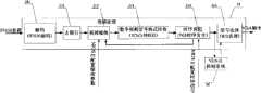
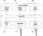
参见图1,视频监视系统一般主要由视频信号转换1(ADV7181B)、视频计算处理/系统控制2、数据存储/通信3、视频显示信号转换4(DAV7213)以及VGA显示5构成;其中视频计算处理/系统控制2由视频处理21和NIOS II控制系统22构成,视频监视系统实现方法如下所述:a.将模拟视频信号输至视频信号转换1(ADV7181B),经视频计算处理/系统控制2中的NIOSII控制系统22控制后,该模拟视频信号转换为数字视频信号以及同步信号I;b.将数字视频信号以及同步信号I经视频计算处理/系统控制2中视频处理21的处理,输出RGB数字视频信号以及同步信号II;c.将视频计算处理/系统控制2中的视频处理21输出的RGB数字视频信号以及同步信号II直接输至视频显示信号转换4(DAV7213),转换为模拟的RGB数字视频信号;或者将视频处理21输出的RGB数字视频信号以及同步信号II经NIOSII控制系统22输至数据存储/通信3中的SDRAM32存储后,输至视频显示信号转换4(DAV7213)转换为模拟的RGB数字视频信号;或者将将视频处理21输出的RGB数字视频信号以及同步信号II经NIOSII控制系统22先输至数据存储/通信3中的串行接口31,后经串行接口31上传至上位机;d.将模拟的RGB数字视频信号输至VGA显示5以供输出。Referring to Fig. 1, the video surveillance system generally mainly consists of video signal conversion 1 (ADV7181B), video calculation processing/
以下结合附图对本发明具体实现方法进行详细阐述,视频处理的主要实现方法参见图2。The specific implementation method of the present invention will be described in detail below in conjunction with the accompanying drawings, and the main implementation method of video processing is shown in FIG. 2 .
[1.1]解码:BT656视频信号以及同步信号I是视频计算处理/系统控制2中的NIOS II控制系统21控制视频信号转换1(ADV7181B),将NTSC/PAL/S-Video模拟视频信号转换为数字视频信号,进行视频解码,输出的标准8位BT656视频信号以及同步信号I,供后端的BT656解码211处理。[1.1] Decoding: BT656 video signal and
BT656解码211要遵守BT.656时序及数据格式得到隔行的YCbCr数字视频信号,同步信号I的输出信号,其中YCbCr数字视频信号具体的可以是4∶4∶4、4∶4∶2等的YCbCr数字视频信号。BT656 decoding 211 will observe the BT.656 timing and data format to obtain the interlaced YCbCr digital video signal, the output signal of the synchronous signal I, wherein the YCbCr digital video signal can specifically be 4: 4: 4, 4: 4: 2, etc. YCbCr digital video signal.
参见图3,视频信号转换2(ADV7181B)输出BT656行信号时序,“80 10…”表示当前视频信号处于行消隐阶段。“FF 00 00 XY”是时间参考代码。当XY的bit6=’1’,是EAV(有效视频结束),bit6=’0’,是SAV(有效视频开始)Cb Y Cr Y…为有效视频信号(占用1440个CCL)。XY时间参考代码参见表1。Referring to Figure 3, video signal conversion 2 (ADV7181B) outputs BT656 line signal timing, "80 10..." indicates that the current video signal is in the line blanking stage. "FF 00 00 XY" is the time reference code. When bit6 of XY='1', it is EAV (End of Active Video), bit6='0', it is SAV (Start of Active Video) Cb Y Cr Y...is an effective video signal (occupies 1440 CCLs). See Table 1 for XY time reference codes.
表1Table 1
XY定义为:XY is defined as:
F=“0”forField 0,F=“1”for Field 1;V=“1”during vertical blanking;H=“0”at SAV H=“1”at EAV;
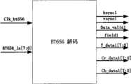
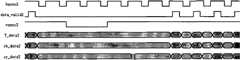
BT656解码211的输入信号是视频信号转换1(ADV7181B)输出的BT656视频信号、同步信号I,输出的是YCbCr数字视频信号及同步信号I。BT656解码主要接口参见图4:Clk_bt656是FPGA 27MHZ时钟;BT656_in[7:0]:视频信号转换1(ADV7181B)输出的BT656视频信号;Hsync1:BT656解码解出的行同步信号I;Vsync1:BT656解码解出的场同步信号I;Data_valid1:BT656解码输出的有效数据信号;Field1:BT656解码输出的场标志信号,0代表偶场,1代表奇场;Y_data1,Cb_data1,Cr_data1:BT656解码输出的YCbCr信号。BT656解码接口时序参见图5。The input signal of
[1.2]去隔行:去隔行212的输入信号是BT656解码211得到的隔行的YCbCr数字视频信号及同步信号I。为节省资源,去隔行采用行复制的转逐行方法,即奇、偶数行每行多复制一行输出。这样,奇、偶数场各可以拼成一帧输出。[1.2] De-interlacing: the input signal of
偶场同步信号I时序及奇场同步信号I时序分别参见图6、图7。Refer to Fig. 6 and Fig. 7 for the timing sequence of the sync signal I of the even field and the timing sequence of the sync signal I of the odd field, respectively.
因为要完整的复制每一行数据,并且要保存下一行的数据,可采用双口RAM来存数据。因视频信号转换2采样的BT656数字视频信号以及同步信号I的传输速率为13.5MHz,而去隔行212输出的YCrCb数字视频信号以及同步信号I的传输速率为27MHz,去隔行211采用双口RAM,去隔行212每一行数据读两次,回复频率,同时完成隔行扫描到逐行扫描的转换。Because it is necessary to completely copy the data of each row and save the data of the next row, a dual-port RAM can be used to store the data. Because the transmission rate of the BT656 digital video signal of
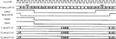
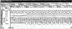
去隔行212采用双口RAM,可缓存一场数据。去隔行212的读写是同时进行。双口RAM工作监测波形参见图8,address_a为写地址计数,地址计数时钟为13.5M.使能地址计数为TD_HS,低电平有效;address_b为读地址计数,地址计数时钟为27M.使能地址计数为BLANK,高电平有效。从信号波形看,address_a和address_b计数相等为720,满足设计要求。同时每写入一场可准确读出两场数据,没有偏差,完全符合设计要求。
去隔行212接口参见图9,Hsync2去隔行212输出的逐行的行同步信号I;Vsync2去隔行212输出的逐行的场同步信号I;Data_valid2去隔行212输出的有效数据信号;Y_data2,Cb_data2,Cr_data2去隔行212输出的YCbCr数字视频信号。De-interlacing 212 interface is referring to Fig. 9, the progressive line synchronization signal I of Hsync2 de-interlacing 212 output; The progressive field synchronizing signal I of Vsync2 de-interlacing 212 output; The effective data signal of Data_valid2 de-interlacing 212 output; Y_data2, Cb_data2,
完整YCbCr输出时序参见图10,当data_valid2为高电平时,YCrCb输出有效视频数据,为低电平时,输出消隐数据,Y输出”0x00”,Cr、Cb输出”0x80”。See Figure 10 for the complete YCbCr output timing. When data_valid2 is high, YCrCb outputs valid video data. When it is low, it outputs blanking data. Y outputs "0x00", and Cr and Cb output "0x80".
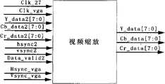
[1.3]视频缩放:将逐行的YCbCr数字视频信号以及逐行的同步信号I通过视频缩放213至YCbCr转RGB214,转换为RGB数字视频信号;[1.3] Video scaling: the progressive YCbCr digital video signal and progressive synchronous signal I are converted to RGB digital video signal by video scaling 213 to YCbCr to RGB214;
[1.4]时序调配:将RGB数字视频信号以及NIOS II配置时钟信号通过VGA时序发生215消隐调配为RGB数字视频信号、同步信号II以及供VGA显示的时钟信号;[1.4] Timing allocation: the RGB digital video signal and NIOS II configuration clock signal are allocated to RGB digital video signal, synchronous signal II and clock signal for VGA display through
[1.5]视频缩放:视频缩放213根据NIOSII配置缩放参数、由去隔行212输出的逐行的同步信号I、以及又VGA时序发生215输出的同步信号II,对由去隔行212输出的YCbCr数字视频信号进行缩放。[1.5] Video scaling: Video scaling 213 configures scaling parameters according to NIOSII, the progressive synchronous signal I output by deinterlacing 212, and the synchronous signal II of
视频缩放213的功能是把输入的视频水平和/或垂直缩放成显示需要的格式。例如将输入的YCbCr数字视频信号以及同步信号I(720X480或720X576)缩小为YCbCr数字视频信号以及同步信号II(640X480)。视频缩放213的接口参见图11,其中Clk_27为系统27MHZ时钟;Clk_vga为系统VGA显示时钟;Hsync_vga,vsync_vga为VGA时序发生215输出的供VGA显示的同步信号II;Y_data,Cb_data,Cr_data为经视频缩放213输出的视频数据信号。The function of the video scaling 213 is to horizontally and/or vertically scale the input video into a format required for display. For example, the input YCbCr digital video signal and synchronous signal I (720X480 or 720X576) are reduced to YCbCr digital video signal and synchronous signal II (640X480). The interface of video scaling 213 is referring to Fig. 11, and wherein Clk_27 is system 27MHZ clock; Clk_vga is system VGA display clock; Hsync_vga, vsync_vga is the synchronous signal II that
视频缩放213具体应用如下的方法来实现,其流程示意图参见图12。The video zooming 213 is specifically implemented by the following method, and its flowchart is shown in FIG. 12 .
1)视频缩放213根据输入的同步信号I和同步信号II计算插值步长,计算:插值步长=同步信号I/同步信号II得插值步长。1) The video scaling 213 calculates the interpolation step size according to the input sync signal I and sync signal II, and calculates: interpolation step size=interpolation step size of sync signal I/sync signal II.
1.1)根据插值步长来确定新像素点X插值位置。1.1) Determine the X interpolation position of the new pixel point according to the interpolation step.
例如输入视频缩放213的逐行同步信号I为720X480,输入视频缩放的同步信号II是640X480,则可得缩放比(640*480)/(720*480)=0.889。根据缩放精度确定以一个或多个有效像素为一个像素点单位。例如每一个有效像素为一个像素点单位,那么得到需要插值的步长是(720x480)/(640*480)=1.125。For example, the progressive synchronous signal I input to the video scaling 213 is 720×480, and the synchronous signal II input to the video scaling 213 is 640×480, then the scaling ratio (640*480)/(720*480)=0.889 can be obtained. One or more effective pixels are determined as a pixel unit according to the scaling precision. For example, each effective pixel is a pixel unit, then the step size required for interpolation is (720x480)/(640*480)=1.125.
参见图13,以原始每个有效像素点的步长为1,则所产生的插值点步长1.125,2.25,3.375…是新像素点的位置即要插值点X的位置,见图示的虚点。虚点表示要产生640X480的一行像素点,实点表示原始720X480的一行像素点。Referring to Fig. 13, if the original step size of each effective pixel is 1, then the generated interpolation point step size 1.125, 2.25, 3.375... is the position of the new pixel point, that is, the position of the point X to be interpolated, see the dotted point in the illustration point. Dotted dots represent a row of pixels of 640X480, and solid dots represent a row of pixels of original 720X480.
2)以16个原始像素点为方阵式区域,形成X1~X16个像素点,得到X位置的像素值即非线性插值结果x_lans。2) Use 16 original pixels as a square matrix area to form X1~X16 pixels, and obtain the pixel value at X position, which is the nonlinear interpolation result x_lans.
从当前像素点周围的16个像素点得到当前像素点的非线性插值结果x_lans。例如以16个原始像素点为方阵,形成X1~X16个像素点,得到X位置的像素值,参见图14。Get the nonlinear interpolation result x_lans of the current pixel from the 16 pixels around the current pixel. For example, 16 original pixels are used as a square matrix to form X1~X16 pixels to obtain the pixel value at X position, see Figure 14.
具体实现方法如下:The specific implementation method is as follows:
2.1)计算方阵的列缩放系数para_v、方阵的行缩放系数para_h、2.1) Calculate the column scaling factor para_v of the square matrix, the row scaling factor para_h of the square matrix,
由于非线性插值函数频谱具有很宽的通带特性,可以得到高频损失较少的插值结果。因此这里用Lanczos非线性插值函数,通过多相位插值以及查找表的形式来实现,表的值可以通过软件来配置。Since the spectrum of the nonlinear interpolation function has a very wide passband characteristic, an interpolation result with less high-frequency loss can be obtained. Therefore, the Lanczos nonlinear interpolation function is used here, which is realized by multi-phase interpolation and look-up table, and the value of the table can be configured by software.
在查找表中,采用128X4个插值,即128个位置,根据函数对称性,可以得到256个采样位置。所以精度可以达到1/256像素位置。In the lookup table, 128X4 interpolations are used, that is, 128 positions. According to the symmetry of the function, 256 sampling positions can be obtained. So the accuracy can reach 1/256 pixel position.
下面的公式是Lanczos非线性插值函数The following formula is the Lanczos nonlinear interpolation function

Lanczos公式中a的值的幅频响应参见图15,这里采用多相位插值函数方式,取插值点周围四个点对应的插值系数para_v1,para_v2,para_v3,para_v4,这四个点每个点之间间隔是单位1,范围是-2<x<2,因此取a=2。The amplitude-frequency response of the value of a in the Lanczos formula is shown in Figure 15. Here, the multi-phase interpolation function method is used to take the interpolation coefficients para_v1, para_v2, para_v3, and para_v4 corresponding to the four points around the interpolation point. Between each point of these four points The interval is
例若取x插值位置为其中某一个值(0/256,1/256,2/256…255/256,256/256),根据下述公式,得到四个插值像素点对应的系数分别是,para_v1,para_v2,para_v3,para_v4。For example, if the interpolation position of x is taken as one of the values (0/256, 1/256, 2/256...255/256, 256/256), according to the following formula, the coefficients corresponding to the four interpolation pixel points are respectively, para_v1, para_v2, para_v3, para_v4.
para_v1=sinc(-1-x)*sinc((-1-x)/2);para_v1=sinc(-1-x)*sinc((-1-x)/2);
para_v2=sinc(-x)*sinc(-x/2);para_v3=sinc(1-x)*sinc((1-x)/2);para_v2=sinc(-x)*sinc(-x/2); para_v3=sinc(1-x)*sinc((1-x)/2);
para_v4=sinc(2-x)*sinc((2-x)/2);para_v4=sinc(2-x)*sinc((2-x)/2);
2.2)确定查找表2.2) Determine the lookup table
将步骤2.1)所得的方阵的列缩放系数para_v、方阵的行缩放系数para_h写入查找表。Write the column scaling factor para_v of the square matrix obtained in step 2.1) and the row scaling factor para_h of the square matrix into the lookup table.
得到查找表参见表2:See Table 2 for the lookup table:
因为所用的插值函数具有偶对称关系,因此,从表2中可看出,偏移x从129/256到256/256和偏移x从127/256到0/256的插值系数具有对称关系,所以只需要从0/256到128/256的查找表系数即可。Because the interpolation function used has an even symmetric relationship, it can be seen from Table 2 that the interpolation coefficients of offset x from 129/256 to 256/256 and offset x from 127/256 to 0/256 have a symmetrical relationship, So only lookup table coefficients from 0/256 to 128/256 are needed.
查表时,比如,当X垂直插值位置是0时,即偏移位置是0/256,通过查找表,可以得到4个插值系数为[0,1,0,0]。当X垂直插值位置是7/256时,即偏移位置是7/256,通过查找表,可以得到4个插值系数为[-0.016,0.998,0.018,0]。When looking up the table, for example, when the X vertical interpolation position is 0, that is, the offset position is 0/256, by looking up the table, four interpolation coefficients can be obtained as [0, 1, 0, 0]. When the X vertical interpolation position is 7/256, that is, the offset position is 7/256, four interpolation coefficients [-0.016, 0.998, 0.018, 0] can be obtained through the lookup table.
同理,可以通过水平偏移,查表得到水平方向的插值系数。Similarly, the interpolation coefficient in the horizontal direction can be obtained by looking up the table through the horizontal offset.
2.3)查找步骤2.2)中所得查找表的方阵的列缩放系数para_v,计算归一化的系数的和sum1以及每列的垂直向系数以确定每列的垂直向系数。2.3) Find the column scaling factor para_v of the square matrix of the resulting lookup table in step 2.2), calculate the sum sum1 of the normalized coefficients and the vertical coefficient of each column to determine the vertical coefficient of each column.
归一化的系数的和sum1为方阵的列缩放系数para_v之和;The sum of the normalized coefficients sum1 is the sum of the column scaling coefficients para_v of the square matrix;
计算:calculate:
垂直向系数X_m1=(X1*para_v1+X5*para_v2+X9*para_v3+X13*para_v4)/sum1Vertical coefficient X_m1=(X1*para_v1+X5*para_v2+X9*para_v3+X13*para_v4)/sum1
垂直向系数X_m2=(X2*para_v1+X6*para_v2+X10*para_v3+X14*para_v4)/sum1Vertical coefficient X_m2=(X2*para_v1+X6*para_v2+X10*para_v3+X14*para_v4)/sum1
垂直向系数X_m3=(X3*para_v1+X7*para_v2+X11*para_v3+X15*para_v4)/sum1Vertical coefficient X_m3=(X3*para_v1+X7*para_v2+X11*para_v3+X15*para_v4)/sum1
垂直向系数X_m4=(X4*para_v1+X8*para_v2+X12*para_v3+X16*para_v4)/sum1Vertical coefficient X_m4=(X4*para_v1+X8*para_v2+X12*para_v3+X16*para_v4)/sum1
则得每列的垂直向系数。Then get the vertical coefficient of each column.
2.4)查找步骤2.2)中所得查找表的方阵的行缩放系数para_h计算水平向归一化的系数的和sum2以确定最终X位置的非线性插值结果X_lans。2.4) Find the row scaling coefficient para_h of the square matrix of the lookup table obtained in step 2.2) and calculate the sum sum2 of the horizontally normalized coefficients to determine the nonlinear interpolation result X_lans of the final X position.
水平向归一化的系数的和sum2为方阵的行缩放系数para_h之和。The sum of the horizontally normalized coefficients sum2 is the sum of the row scaling coefficients para_h of the square matrix.
计算:X_lans=(X_m1*para_h1+X_m2*para_h2+X_m3*para_h3+X_m4*para_h4)/sum2得非线性插值结果X_lans。Calculation: X_lans=(X_m1*para_h1+X_m2*para_h2+X_m3*para_h3+X_m4*para_h4)/sum2 to get the nonlinear interpolation result X_lans.
2.5)为了控制视频插值点的平滑度,需要对插值结果X进行过冲和下冲控制。具体实现方法是:2.5) In order to control the smoothness of video interpolation points, it is necessary to control the overshoot and undershoot of the interpolation result X. The specific implementation method is:
2.5.1)选取方阵相邻列的原始像素点位置的最大值XL_max以及方阵相邻列的原始像素点位置的最小值XL_min。2.5.1) Select the maximum value XL_max of the original pixel positions of the adjacent columns of the square array and the minimum value XL_min of the original pixel positions of the adjacent columns of the square array.
即:XL_max=MAX(X6,X7,X10,X11);XL_min=MIN(X6,X7,X10,X11)Namely: XL_max=MAX(X6, X7, X10, X11); XL_min=MIN(X6, X7, X10, X11)
2.5.2)根据设计要求选择n位过冲控制门限0T_ctrl和n位下冲控制门限UT_ctrl,其范围是0~63。2.5.2) Select n-bit overshoot control threshold 0T_ctrl and n-bit undershoot control threshold UT_ctrl according to design requirements, and the range is 0~63.
2.5.3)判定过冲和下冲控制以确定非线性插值结果X_lans1。2.5.3) Determine the overshoot and undershoot control to determine the nonlinear interpolation result X_lans1.
2.5.3.1)将经步骤2.4)所得的非线性插值结果X_lans与原始像素点位置的最大值XL_max进行比较后,控制过冲,确定非线性插值结果X_lans1。2.5.3.1) After comparing the nonlinear interpolation result X_lans obtained in step 2.4) with the maximum value XL_max of the original pixel position, control the overshoot and determine the nonlinear interpolation result X_lans1.
2.5.3.2)将经步骤2.4)所得的非线性插值结果X_lans与原始像素点位置的最小值X_min进行比较后,进行下冲控制,确定非线性插值结果X_lans1。2.5.3.2) After comparing the nonlinear interpolation result X_lans obtained in step 2.4) with the minimum value X_min of the original pixel position, perform undershoot control to determine the nonlinear interpolation result X_lans1.
X_lans>X_max,则X_lans1=X_lans-(X_lans-X_max)*0T_ctrl/64;X_lans>X_max, then X_lans1=X_lans-(X_lans-X_max)*0T_ctrl/64;
若X_lans<X_min,则X_lans1=X_lans+(X_min-X_lans)*UT_ctrl/64If X_lans<X_min, then X_lans1=X_lans+(X_min-X_lans)*UT_ctrl/64
最终插值结果X_lans1要限制在0~255,若X_lans1>255则确定非线性插值结果X_lans1的值为255;若X_lans1<0则确定非线性插值结果X_lans1的值为0。The final interpolation result X_lans1 should be limited to 0~255. If X_lans1>255, the value of the nonlinear interpolation result X_lans1 is determined to be 255; if X_lans1<0, the value of the nonlinear interpolation result X_lans1 is determined to be 0.
3)通过线性插值方法,从当前像素点周围的16个像素点得到当前像素点的线性插值结果x_bi。3) Obtain the linear interpolation result x_bi of the current pixel from 16 pixels around the current pixel through the linear interpolation method.
具体实现方法如下:The specific implementation method is as follows:
3.1)计算:3.1) Calculation:
待插值的水平左点LL1=[X1*N_ctrl1+X2*(64-N_ctrl1)]/64Horizontal left point LL1 to be interpolated = [X1*N_ctrl1+X2*(64-N_ctrl1)]/64
待插值的水平右点LR1=[X4*N_ctrl1+X3*(64-N_ctrl1)]/64Horizontal right point LR1 to be interpolated=[X4*N_ctrl1+X3*(64-N_ctrl1)]/64
待插值的水平左点LL2=[X5*N_ctrl1+X6*(64-N_ctrl1)]/64Horizontal left point LL2 to be interpolated=[X5*N_ctrl1+X6*(64-N_ctrl1)]/64
待插值的水平右点LR2=[X8*N_ctrl1+X7*(64-N_ctrl1)]/64Horizontal right point LR2 to be interpolated=[X8*N_ctrl1+X7*(64-N_ctrl1)]/64
待插值的水平左点LL3=[X9*N_ctrl1+X10*(64-N_ctrl1)]/64Horizontal left point LL3 to be interpolated = [X9*N_ctrl1+X10*(64-N_ctrl1)]/64
待插值的水平右点LR3=[X12*N_ctrl1+X11*(64-N_ctrl1)]/64Horizontal right point LR3 to be interpolated = [X12*N_ctrl1+X11*(64-N_ctrl1)]/64
待插值的水平左点LL4=[X13*N_ctrl1+X14*(64-N_ctrl1)]/64Horizontal left point LL4 to be interpolated = [X13*N_ctrl1+X14*(64-N_ctrl1)]/64
待插值的水平右点LR4=[X16*N_ctrl1+X15*(64-N_ctrl1)]/64Horizontal right point LR4 to be interpolated=[X16*N_ctrl1+X15*(64-N_ctrl1)]/64
其中n位门限N_ctrl1选取范围为0~63,得待插值的水平左右点。Among them, the selection range of the n-bit threshold N_ctrl1 is 0~63, and the left and right points of the level to be interpolated are obtained.
3.2)计算:3.2) Calculation:
线性插值点X_l1=LL1*(1-x_offset)+LR1*x_offset,Linear interpolation point X_l1=LL1*(1-x_offset)+LR1*x_offset,
线性插值点X_l2=LL2*(1-x_offset)+LR2*x_offset,Linear interpolation point X_l2=LL2*(1-x_offset)+LR2*x_offset,
线性插值点X_l3=LL3*(1-x_offset)+LR3*x_offset,Linear interpolation point X_l3=LL3*(1-x_offset)+LR3*x_offset,
线性插值点X_l4=LL4*(1-x_offset)+LR4*x_offset,Linear interpolation point X_l4=LL4*(1-x_offset)+LR4*x_offset,
其中x_offset为水平向偏移量,得线性插值点。Among them, x_offset is the horizontal offset, and the linear interpolation point is obtained.
3.3)计算:3.3) Calculation:
垂直方向的上点X_UP=[X_l1*N_ctrl1+X_l2*(64-N_ctrl1)]/64,The upper point X_UP in the vertical direction=[X_l1*N_ctrl1+X_l2*(64-N_ctrl1)]/64,
垂直方向的下点X_DN=[X_l3*N_ctrl1+X_l4*(64-N_ctrl1)]/64,The lower point X_DN in the vertical direction=[X_l3*N_ctrl1+X_l4*(64-N_ctrl1)]/64,
得垂直方向上的点X_UP及垂直方向的下点X_DN。Get the point X_UP in the vertical direction and the down point X_DN in the vertical direction.
3.4)计算:3.4) Calculation:
线性插值结果X_bi=X_UP*(1-y_offset)+X_DN*y_offset,其中y_offset为垂直向偏移量。The linear interpolation result X_bi=X_UP*(1-y_offset)+X_DN*y_offset, where y_offset is the vertical offset.
得线性插值结果X_bi。Get the linear interpolation result X_bi.
在噪声情况下,线性插值可以得到较好的插值效果,因为其低通滤波特性使其有很好的降噪的功能。In the case of noise, linear interpolation can get a better interpolation effect, because its low-pass filtering characteristics make it have a good noise reduction function.
4)通过自适应判断确定最终插值结果:4) Determine the final interpolation result through adaptive judgment:
将线性插值结果X_bi与非线性插值结果X_lans1进行对比以确定最终插值结果。The linear interpolation result X_bi is compared with the nonlinear interpolation result X_lans1 to determine the final interpolation result.
4.1)选取原16个像素点的位置的最大值Ymax,选取原16个像素点的位置的最小值Ymin。4.1) Select the maximum value Ymax of the positions of the original 16 pixels, and select the minimum value Ymin of the positions of the original 16 pixels.
4.2)将原16个像素点的位置的最大值Ymax与原16个像素点的位置的最小值Ymin的差值和n位门限N_ctrl2进行比较,确定插值结果。4.2) Compare the difference between the maximum value Ymax of the original 16 pixel positions and the minimum value Ymin of the original 16 pixel positions with the n-bit threshold N_ctrl2 to determine the interpolation result.
若原16个像素点的位置的最大值Ymax-原16个像素点的位置的最小值Ymin>n位门限N_ctrl2,则插值结果为线性插值X_bi;若原16个像素点的位置的最大值Ymax-原16个像素点的位置的最小值Ymin<n位门限N_ctrl2,则插值结果为非线性插值结果X_lans,其中n位门限N_ctrl2的取值范围为0~63。If the maximum value Ymax of the original 16 pixel positions - the minimum value Ymin of the original 16 pixel positions > n-bit threshold N_ctrl2, the interpolation result is linear interpolation X_bi; if the maximum value Ymax of the original 16 pixel positions - the original If the minimum value Ymin of the positions of 16 pixels<n-bit threshold N_ctrl2, the interpolation result is nonlinear interpolation result X_lans, where the value range of n-bit threshold N_ctrl2 is 0~63.
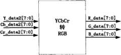
[1.6]数字视频信号格式转换:由视频缩放213输出的缩放的YCbCr数字视频信号输至YCbCr转RGB214,经YCbCr转RGB 214转换后得到的RGB数字视频信号输至VGA时序发生215。[1.6] Digital video signal format conversion: the zoomed YCbCr digital video signal output by
YCrCb转RGB214接口参见图16。其中Y_data2,Cb_data2,Cr_data2为从视频缩放输出的数据;Y_data2指亮度,Cb_data2指蓝色分量,Cr_data2指红色分量。输出是转换了的RGB数据,R_data指红色,G_data指绿色,B_data指蓝色。Refer to Figure 16 for the interface of YCrCb to RGB214. Among them, Y_data2, Cb_data2, and Cr_data2 are the output data from video scaling; Y_data2 refers to the brightness, Cb_data2 refers to the blue component, and Cr_data2 refers to the red component. The output is converted RGB data, R_data refers to red, G_data refers to green, B_data refers to blue.
所用转化方阵如下式所示:The transformation matrix used is as follows:
R=Y+1.403Cr=Y+Cr+0.403Cr=Y+Cr+0x19CCrR=Y+1.403Cr=Y+Cr+0.403Cr=Y+Cr+0x19CCr
为计算方便把0x19C表示为小数0.403右移10位的十六进制计算出的R,G,B最后还要通过纠正,因有些坏值使RGB值大于1023或小于0。当大于1023时,纠正RGB值为1023,小于0时,RGB赋值0。这样RGB可用10位二进制来表示。For the convenience of calculation, 0x19C is expressed as a decimal 0.403 shifted to the right by 10 digits. The R, G, and B calculated in hexadecimal have to be corrected at last, because some bad values make the RGB value greater than 1023 or less than 0. When it is greater than 1023, the corrected RGB value is 1023, and when it is less than 0, the RGB value is assigned 0. In this way, RGB can be expressed in 10-bit binary.
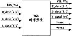
[1.7]时序调配:RGB数字视频信号以及NIOS II配置时钟信号输入VGA时序发生215进行调配,经VGA时序发生215调配后输出的同步信号II、RGB数字视频信号以及供VGA显示的时钟信号一路输至MUX选择;另一路经NIOSII控制系统22输至MUX选择216;同时经VGA时序发生215消隐调配后输出的同步信号II反馈至视频缩放213。[1.7] Timing deployment: RGB digital video signal and NIOS II configuration clock signal are input to
VGA时序发生215产生VGA显示需要的时序,与输出有效数据同步,产生标准的640*480的VGA显示数据的行场同步信号II。The
一般计算机VGA(640×480,60Hz)图像格式的信号时序,其点时钟DCLK为25.175MHz,场频为59.94Hz。场周期为16.683ms,每场有525行,其中480行为有效显示行,45行为场消隐期。场同步信号Vs每场有一个脉冲,该脉冲的低电平宽度为63μs(2行)。场消隐期包括场同步时间、场消隐前肩(13行)、场消隐后肩(30行),共45行。行周期为31.78μs,每显示行包括800点,其中640点为有效显示,160点为行消隐期(非显示区)。行同步信号Hs每行有一个脉冲,该脉冲的低电平宽度为3.81μs(即96个DCLK);行消隐期包括行同步时间,行消隐前肩(19个DCLK)和行消隐后肩(45个DCLK),共160个点时钟。复合消隐信号是行消隐信号和场消隐信号的逻辑与,在有效显示期复合消隐信号为高电平,在非显示区域它是低电平。For the signal timing of the general computer VGA (640×480, 60Hz) image format, the dot clock DCLK is 25.175MHz, and the field frequency is 59.94Hz. The field cycle is 16.683ms, and each field has 525 lines, of which 480 lines are effectively displayed, and 45 lines are blanked. The field sync signal Vs has a pulse in each field, and the low-level width of the pulse is 63μs (2 lines). Vertical blanking period includes vertical synchronization time, vertical blanking front porch (13 lines), vertical blanking back porch (30 lines), 45 lines in total. The line cycle is 31.78μs, and each display line includes 800 points, of which 640 points are effective display and 160 points are line blanking period (non-display area). The line synchronization signal Hs has one pulse per line, and the low-level width of the pulse is 3.81 μs (that is, 96 DCLKs); the line blanking period includes line synchronization time, line blanking front shoulder (19 DCLKs) and line blanking Back shoulder (45 DCLK), a total of 160 o'clock. The composite blanking signal is the logic AND of the line blanking signal and the vertical blanking signal. The composite blanking signal is high level during the effective display period, and it is low level in the non-display area.
VGA时序发生215接口参见图17。其中Clk_vga为VGA的显示时钟,也是模块的时钟。R_data1,g_data1,b_data1为输出给视频显示信号转换4(DAV7213)的最终数据。Hsync,vsync,是输出给视频显示信号转换4(DAV7213)的同步信号II,也是给视频缩放213输入的信号。Refer to FIG. 17 for the
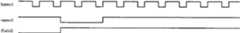
行同步信号II(hsync)产生的时序参见图18,其中第一个下降沿到第二个下降沿为一个完整周期,共800个像素点,其中有效像素点为640个。See Figure 18 for the timing sequence of the horizontal synchronization signal II (hsync), where the first falling edge to the second falling edge is a complete cycle, with a total of 800 pixels, of which 640 are effective pixels.
场同步信号II(vsync)产生的时序参见图19第一个下降沿到第二个下降沿为一个完整周期,共525个行,其中有效像行为480个。For the timing sequence of the vertical synchronization signal II (vsync), refer to Figure 19. The first falling edge to the second falling edge is a complete cycle, with a total of 525 lines, of which 480 effective image lines.
[1.8]信号选择:VGA时序发生215输出的RGB数字视频信号、同步信号II以及供VGA显示的时钟信号直接经MUX选择216输出供VGA显示,或VGA时序发生215输出的RGB数字视频信号、同步信号II以及供VGA显示的时钟信号经NIOS II控制系统22控制后再经MUX选择216输出供VGA显示。[1.8] Signal selection: RGB digital video signal output by
参见图20,NIOSII控制系统22主要由NIOSIICPU224、采集控制核225、SDRAM控制核221、DMA控制核223、串行接口控制核222以及VGA控制核226构成。Referring to FIG. 20 , the
在SOPC中添加了用户自定义外设,简化硬件的设计。在SOPCBuilder中生成的NIOSII控制系统22的硬件连接参见图21。其中Cpu_0为NIOSII CPU;tri_state_bridge为Avalon总线;timer0,timer1为定时器;sdram为SDRAM控制核;button_pio,switch_pio为输入/输出端口;Dma为DMA控制核;UART_0为串行接口(UART)控制核;Vga为VGA控制核,to_sdram为采集控制核。User-defined peripherals are added to SOPC to simplify hardware design. Refer to FIG. 21 for the hardware connection of the
NIOSII控制系统22的控制方法主要包括以下步骤:The control method of
[2.1]NIOSIICPU224控制采集控制核225将视频处理21输出的数据经DMA控制核223传输到SDRAM控制核221和串行接口控制核222;[2.1] NIOSIICPU224 control gathers
[2.2]NIOSIICPU224控制SDRAM控制核221中的数据经DMA控制核223存至SDRAM32;[2.2] NIOSIICPU224 controls the data in
[2.3]NIOSIICPU224控制VGA控制核226将转换后的数据输出至视频处理21;[2.3] NIOSIICPU224 controls
[2.4]NIOSIICPU224控制SDRAM控制核221将数据经DMA控制核223送至VGA控制核226;[2.4] NIOSIICPU224 controls
[2.5]NIOSIICPU224控制串行接口控制核222将采集控制核225中的数据传输至上位机。[2.5] NIOSIICPU224 controls the serial
以下结合附图对于NIOSII控制系统22中的相关控制核进行详细的阐述。The relevant control cores in the
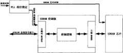
SDRAM芯片时钟和AVALON总线接口的时钟驱动必须同步,像其它的同步设计,必须确保地址,数据,控制信号在时钟边沿到来时必须保持稳定。所以必须用锁相环PLL在SDRAM控制核221和SDRAM芯片之间稳定时钟。在低速时钟的时候,时钟相对延时较小,锁相环PLL可以不用。SDRAM控制核221接口示意图参见图22。The SDRAM chip clock and the clock driver of the AVALON bus interface must be synchronized. Like other synchronous designs, it is necessary to ensure that the address, data, and control signals must remain stable when the clock edge arrives. Therefore, a phase-locked loop PLL must be used to stabilize the clock between the
AVALON从接口是SDRAM控制核221的用户接口部分。当访问从接口时,SDRAM控制核221整个传输协议对用户是透明的。可通过控制逻辑控制AVALON从接口的地址(Adress),数据(Data),等待请求(Waitrequest),读取数据有效(Readdatavalid)信号经由SDRAM接口适配处理后来实现SDRAM芯片读写操作。The AVALON slave interface is the user interface part of the
时钟源(Clock source)是NIOSII控制系统22时钟50Mhz,通过锁相环PLL相位调整,产生50MHZSDRAMclock(SDRAM芯片时钟)和50MHz不同相位的SDRAM控制核时钟(controllerclock)。The clock source (Clock source) is
在NIOSII控制系统22设计中,采用DMA控制核传输SDRAM的数据操作,视频数据通过AVALON总线由DMA方式传输到SDRAM控制核221。通过SDRAM控制核221将视频数据批量写入SDRAM32。In the design of the
DMA控制核223由AVALON从接口控制实现批量数据的传输。主读端口(READ MASTER PORT)连接读数据源模块,主写端口(WRITE MASTER PORT)连接写数据目的模块。DMA控制核可以非常有效的传输数据,只要配置好DMA控制核内部寄存器,连接好读写模块,DMA控制核就可以批量的传输数据。当DMA控制核传输结束时,DMA控制核223发出中断请求信号,NIOSIICPU224可对其响应。DMA控制核223接口示意图参见图23.The
采集的视频数据通过AVALONG总线端口传输到的DMA控制核223,通过NIOSIICPU224控制DMA控制核223批量传输视频数据到SDRAM控制核221。The collected video data is transmitted to the
串行接口(UART)控制核222为嵌入式系统和外部器件之间通信传输提供了方便。串行接口(UART)控制核222遵守RS-232协议时序经波特率分频提供了可调的波特率,奇偶校验位,停止位和数据位。串行接口控制核222接口示意图参见图24。The serial interface (UART)
串行接口控制核222连接AVALON从接口,经由控制寄存器将并行数据转换成串行数据后上传至上位机;输入的串行数据经由控制寄存器转换为并行数据后传至AVALON从接口从而实现了串行接口通信。The serial
采集控制核225主要由采集模块和FIFO传输模块构成,NIOSIICPU224控制采集控制核225中的采集模块采集视频处理21输出的数据,并将数据写入采集控制核225中的FIFO传输模块。The
采集控制核225符合Avalon总线规范,该采集控制核225将视频处理21输出的的数据通过DMA控制核223完整送入SDRAM控制核,实现数据的存储和处理。The
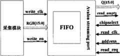
视频处理21输出的数据频率是27MHz,每帧图像数据为640×480×16bit像素。然而NIOSIICPU224工作时钟为50MHz,因此需要FIFO传输模块实现前后传输的连贯性。采集控制核225结构示意图参见图25。The data frequency output by the
采集控制核225包括采集模块和FIFO传输模块。采集模块实现视频处理21输出数据的采集,其输入接口有:写时钟(write_clk)、写使能(write_en)与16位数据总线(RGB[15:0])。挂在Avalon总线上的接口有数据输出总线(FIFO Q[15:0])、片选信号(chipselect)、读请求信号(read_req)、Avalon总线地址(address)、读空信号(read_empty)、读时钟(read_clk)。The
使用视频处理21输出的同步信号II(RGB USEFUL)作为写使能信号,NIOSIICPU224控制采集控制核225中的采集模块向FIFO传输模块写数据。由于FIFO传输模块输出时钟大于写时钟,所以不会将FIFO传输模块写满,而只会读空FIFO传输模块。所以读请求信号(read_req)由Avalon总线发出,经读空信号(read_empty),由NIOSIICPU控制DMA控制核读取FIFO传输模块中数据的时间,在读空信号(read_empty)为低电平即FIFO传输模块为非空时开始读取FIFO传输模块中的数据。Avalon总线的从端口读取传输的数据时序参见图26,其中有效RGB数据信号(Data available)接FIFO传输模块输出的读空信号(read_empty)。FIFO传输模块仿真波形参见图27。Use the synchronous signal II (RGB USEFUL) that
参见图26,当FIFO传输模块非空,即Data available为1时,Avalon总线的片选信号(chipselect)、读使能信号(read_en)同时为高,读取FIFO传输模块输出的数据;当FIFO传输模块为空时,即有效数据(Data available)为0时,Avalon总线的片选信号(chipselect)、读使能信号(read_en)同时为低,等待读取FIFO传输模块的数据,直到FIFO传输模块非空时,Avalon总线的片选信号(chipselect)、读使能信号(read_en)同时为高,继续读取数据。Referring to Figure 26, when the FIFO transmission module is not empty, that is, when Data available is 1, the chip select signal (chipselect) and the read enable signal (read_en) of the Avalon bus are high at the same time, and the data output by the FIFO transmission module is read; when the FIFO When the transmission module is empty, that is, when the valid data (Data available) is 0, the chip select signal (chipselect) and the read enable signal (read_en) of the Avalon bus are low at the same time, waiting to read the data of the FIFO transmission module until the FIFO transmission When the module is not empty, the chip select signal (chipselect) and the read enable signal (read_en) of the Avalon bus are high at the same time, and continue to read data.
VGA控制核226包括VGA时序发生器、FIFO存储模块其结构示意图参见图28。通过Avalon总线接口的RGB数字视频信号、同步信号II、输至VGA控制核226然后输出到视频显示信号转换4。The
参见图29,当FIFO存储模块非满时,即读数据(read for data)为1时,Avalon总线的片选信号(chipselect),写信号(write)同时为高,FIFO存储模块读取Avalon总线输出数据,当FIFO存储模块写满时,即读数据(read for data)为0时,Avalon总线的片选信号(chipselect),写信号(write)同时为低,FIFO存储模块等待Avalon总线输出数据,直到FIFO存储模块非满时,Avalon总线的片选信号(chipselect),写信号(write)同时为高,FIFO存储模块继续读取Avalon总线输出数据。Referring to Figure 29, when the FIFO storage module is not full, that is, when the read data (read for data) is 1, the chip select signal (chipselect) and the write signal (write) of the Avalon bus are high at the same time, and the FIFO storage module reads the Avalon bus Output data, when the FIFO storage module is full, that is, when the read data (read for data) is 0, the chip select signal (chipselect) and the write signal (write) of the Avalon bus are low at the same time, and the FIFO storage module waits for the Avalon bus to output data , until the FIFO storage module is not full, the chip select signal (chipselect) and the write signal (write) of the Avalon bus are high at the same time, and the FIFO storage module continues to read the output data of the Avalon bus.
由于NIOSIICPU224系统时钟为50MHz,而VGA显示时序发生输入时钟为25MHz,这需要FIFO存储模块起一个缓冲作用,而控制FIFO存储模块读写数据的是另一个外设——DMA控制核223。在NIOSII控制系统22中,NIOSIICPU224控制采集控制核225采集的视频处理21输出的数据,NIOSIICPU224控制SDRAM控制核221将采集的数据经由DMA控制核223存入SDRAM32。然后使用DMA控制核223提供数据传输通道,并且控制FIFO存储模块读写使能,使FIFO存储模块在50MHz和25MHz的时钟频率调配时数据不溢出。从FIFO存储模块以25MHz时钟读出的数据经过VGA时序发生器产生VGA需要的同步信号II、RGB数字视频信号、供VGA显示的时钟信号。Since the NIOSIICPU224 system clock is 50MHz, and the VGA display timing input clock is 25MHz, this requires the FIFO storage module to act as a buffer, and another peripheral device—
单独对VGA时序发生器进行仿真,其仿真后波形图参见图30。The VGA timing generator is simulated separately, and the waveform diagram after simulation is shown in Figure 30.
步骤[2.2]中的具体实现方法如下,其流程示意图参见图31。The specific implementation method in step [2.2] is as follows, and its flowchart is shown in Figure 31.
(1)初始化DMA控制核:按照设计要求配置DMA控制核的内部寄存器。(1) Initialize the DMA control core: configure the internal registers of the DMA control core according to the design requirements.
初始化DMA控制核223主要是配置DMA控制核223的寄存器参数。DMA控制核223共有5个寄存器。分别是:Initializing the
状态寄存器:寄存器的每位代表DMA控制核223当前传输状态,可通过读该寄存器值判断DMA控制核223的状态,该寄存器的值不能写入。状态寄存器包括传输完成标志(done)、忙碌标志(busy)、DMA控制核223传输完毕是由于读端口发出包结束事件(reop)、DMA控制核223传输完毕是由于写端口发出包结束事件(weop)、DMA控制核223传输完毕是由于传输字节数满足指定长度(len)。Status register: each bit of the register represents the current transmission status of the
读地址寄存器:向此寄存器写入DMA控制核223读取外端口或SDRAM芯片的地址。Read address register: write the address of the
写地址寄存器:向此寄存器写入DMA控制核223输出外端口或SDRAM芯片的地址。Write address register: write the address of the external port or SDRAM chip output by the
传输字节长度寄存器:规定DMA控制核223传输的总字节长度,DMA控制核223每传输一字节寄存器值减1,直到寄存器值为0时,DMA控制核223传输结束。Transmission byte length register: specify the total byte length transmitted by the
控制寄存器:控制DMA控制核223传输数据的方式。控制寄存器每位的名称及其功能描述见表3,DMA控制核223的传输方式、传输方向、传输性质(地址的固定性)及其他使能均由控制寄存器控制。Control registers: control the way in which the
表3table 3
初始化DMA控制核223首先将控制寄存器和状态寄存器清零,向长度寄存器(LENGTH)写入需要传输的数据长度,接着配置主读端口开始地址、主写端口的开始地址,最后配置控制寄存器,使DMA控制核223处于从固定地址读数据、使能DMA控制核223传输、半字节传输状态。此功能是从FIFO传输模块中读取数据传输到SDRAM32中。因此,在该模块中,DMA控制核223的工作是将长度为640×480×16的一帧图片数据从主读端口(地址为0x00c010b8)写入主写端口(SDRAM的指针基地址)。对照表3将控制寄存器配置成394,完成采集数据的存储。Initialization
配置完DMA控制核223的传输参数后,便可控制DMA控制核223读取数据。DMA控制核223开始从FIFO传输模块读数据的使能信号由NIOSII控制系统22的写控制开关和有效像素信号提供。一旦使能DMA控制核223,DMA控制核223自行传输,NIOSIICPU224可处理别的事务,只要处理DMA控制核223何时终止传输即可。在软件里通过DMA控制核223的使能信号调用DMA控制核223传输函数,每使能一次DMA传输,可传送一帧图像数据存入系统主内存。After the transmission parameters of the
若读取存放于SDRAM32的多帧图像数据,用NIOS IICPU224直接调度传输会耗费太多NIOSIICPU224资源且不宜控制,而DMA控制核223可实现大量数据的传输,控制简单,准确率高。If reading multi-frame image data stored in SDRAM32, using NIOS IICPU224 to directly schedule transmission will consume too much NIOSCPU224 resources and is not suitable for control, while
(2)使能DMA控制核223(2) Enable
对DMA控制核223进行使能以判定DMA控制核223能否传输数据;Enabling the
(3)数据存储(3) Data storage
(3.1)判定FIFO传输模块是否为空:(3.1) Determine whether the FIFO transmission module is empty:
若FIFO传输模块为空,则执行DMA控制核223等待。If the FIFO transmission module is empty, the
若FIFO传输模块为非空,则DMA控制核223控制FIFO传输模块将图像数据存储至SDRAM32。If the FIFO transmission module is not empty, the
(3.2)判定存储至SDRAM32的图像数据是否为一帧,当一帧数据未存完,则返回至步骤(3.1);(3.2) determine whether the image data stored to SDRAM32 is a frame, and when a frame of data has not been stored, then return to step (3.1);
(3.3)当一帧数据已存完,判断是否有下一帧数据等待存储;当没有下一帧数据等待存储时,则结束存储;(3.3) When a frame of data has been stored, it is judged whether there is a next frame of data waiting to be stored; when there is no next frame of data waiting to be stored, the storage is ended;
(3.4)当有下一帧数据等待存储时,判定SDRAM32是否存满,若SDRAM32未存满则返回至步骤(1);若SDRAM32已存储满,则结束数据存储。(3.4) When the next frame of data is waiting to be stored, determine whether the SDRAM32 is full, if the SDRAM32 is not full, then return to step (1); if the SDRAM32 is full, then end the data storage.
DMA控制核223传输过程具体实现过程如下:The specific implementation process of the
a)NIOSIICPU224通过其控制端口(control port)配置DMA控制核223,准备启动DMA控制核223传输。a) NIOSIICPU224 configures
b)NIOSIICPU224启动DMA控制核223,DMA控制核223进行传输,即DMA控制核223开始在没有NIOSIICPU224干涉的情况下传送数据。b) NIOSCPU224 starts the
c)DMA控制核223的主写端口从读地址读取数据,然后向FIFO传输模块依序写入数据,DMA控制核223的主写端口从FIFO存储模块中读取数据并向目标地址写入数据;在传输过程中可以不需要NIOSIICPU224干预,但NIOSIICPU224可以终止当前的DMA控制核223传输过程。c) The main write port of the
d)当传送数据达到指定长度或者遇到结束符(EOP),DMA控制核223传输结束,DMA控制核223将产生一个DMA控制核223传输结束中断。d) When the transmitted data reaches the specified length or encounters an end character (EOP), the
图像数据输出的具体实现方法如下:图像显示流程示意图参见图32。The specific implementation method of image data output is as follows: Refer to Figure 32 for a schematic diagram of the image display process.
1)按照设计要求配置DMA控制核223的内部寄存器,对DMA控制核223进行初始化;1) configure the internal registers of the
初始化配置DMA控制核223的控制寄存器,状态寄存器,中断函数,及读写地址,具体配置如下所示:Initialize and configure the control register of the
void init_dma()void init_dma()
{alt_irq_register(DMA_0_IRQ,NULL,DMA_0_isr);{alt_irq_register(DMA_0_IRQ, NULL, DMA_0_isr);
IOWR_ALTERA_AVALON_DMA_CONTROL(DMA_0_BASE,0x00);IOWR_ALTERA_AVALON_DMA_CONTROL(DMA_0_BASE, 0x00);
IOWR_ALTERA_AVALON_DMA_STATUS(DMA_0_BASE,0x00);IOWR_ALTERA_AVALON_DMA_STATUS(DMA_0_BASE, 0x00);
IOWR_ALTERA_AVALON_DMA_LENGTH(DMA_0_BASE,LENTH);IOWR_ALTERA_AVALON_DMA_LENGTH(DMA_0_BASE, LENTH);
IOWR_ALTERA_AVALON_DMA_RADDRESS(DMA_0_BASE,FRAME_BUFFER[0]);IOWR_ALTERA_AVALON_DMA_RADDRESS(DMA_0_BASE, FRAME_BUFFER[0]);
IOWR_ALTERA_AVALON_DMA_WADDRESS(DMA_0_BASE,0x00C010B4);IOWR_ALTERA_AVALON_DMA_WADDRESS(DMA_0_BASE, 0x00C010B4);
IOWR_ALTERA_AVALON_DMA_CONTROL(DMA_0_BASE,730);IOWR_ALTERA_AVALON_DMA_CONTROL(DMA_0_BASE, 730);
}}
2)对DMA控制核223进行使能以判定DMA控制核223能传输数据;2) enabling the
3)应用DMA控制核223中断将图像数据写入FIFO存储模块3) apply
3.1)判定FIFO存储模块是否为满?3.1) Determine whether the FIFO storage module is full?
若FIFO存储模块为满,则执行DMA控制核223等待;If the FIFO storage module is full, then execute
若FIFO存储模块为非满,则DMA控制核223控制FIFO存储模块读取SDRAM32中的数据并将其写入FIFO存储模块;If the FIFO storage module is non-full, the
3.2)判定是否刷新FIFO存储模块,当一帧数据未写完,则返回至步骤3.1);3.2) determine whether to refresh the FIFO storage module, when a frame of data is not finished, then return to step 3.1);
3.3)当一帧数据已写完,刷新FIFO存储模块,判断是否有下一帧数据等待写入;当有下一帧数据等待写入时,则返回至步骤1);3.3) When a frame of data has been written, refresh the FIFO storage module to determine whether there is a next frame of data waiting to be written; when there is a next frame of data waiting to be written, then return to step 1);
3.4)当没有下一帧数据等待写入时,判定是否停止向FIFO存储模块中写入数据;当不停止向FIFO存储模块中写入数据时,返回至步骤1),当停止向FIFO存储模块中写入数据时,则结束写入数据至FIFO存储模块。3.4) When there is no next frame of data waiting to be written, determine whether to stop writing data to the FIFO storage module; when not stopping writing data to the FIFO storage module, return to step 1), When data is written in, the data is written to the FIFO memory module.
与采集图像数据到SDRAM32方式不同,DMA控制核223传输数据到VGA要保持图像静止显示或连续幻灯片播放,用到了DMA控制核223中断函数。其作用就是要保持图片数据发送的连续性。当DMA控制核223发送完一场数据,便产生中断信号,使DMA控制核223的状态寄存器的值发生改变,随即进入中断函数,发送另一场数据。这里碰到的问题是DMA控制核223一旦进入中断函数,为保持画面的稳定就要不间断的传输数据,占用数据总线,若NIOSIICPU224处理别的数据,就会对DMA控制核223传输数据总线产生影响,画面就会产生抖动。为解决此问题只能使NIOSIICPU224在显示静态画面时,处于等待状态。等结束显示静态画面信号有效时,NIOSIICPU224才能正常工作。Different from the method of collecting image data to SDRAM32, the
串行接口(UART)控制核222实现图像数据传输具体流程参见图33。和DMA控制核223传输设置相似,通过设置串行接口(UART)控制核222相应的寄存器,执行不同的串行接口(UART)控制核操作,但注意的是串行接口(UART)控制核222传输的是字节,而存储的数据格式是字型。根据表4串行接口(UART)控制核222的内部寄存器说明,通过配置相应的寄存器可以使能、结束、初始化串行接口(UART)控制核222的传输。Refer to FIG. 33 for the specific flow of image data transmission implemented by the serial interface (UART)
表4Table 4
通过配置串行接口(UART)控制核222的状态寄存器和控制寄存器结束串行接口(UART)控制核222的传输。The transmission of the serial interface (UART)
变量赋初值,状态,控制寄存器的准备接收和准备发送位置‘1’,等待进入串行接口(UART)控制核222中断。进入串行接口(UART)控制核222中断后,依据串行接口31(UART)协议进行数据传输,当一帧图像数据传送完毕时,结束串行接口(UART)控制核222传输,跳出串行接口(UART)控制核222中断。Variable assignment initial value, state, the ready-to-receive and ready-to-send position '1' of the control register, wait to enter the serial interface (UART)
Claims (9)
Translated fromChinese
Priority Applications (1)
| Application Number | Priority Date | Filing Date | Title |
|---|---|---|---|
| CN 200910254404CN101742316B (en) | 2009-12-18 | 2009-12-18 | NIOS II-based video processing method |
Applications Claiming Priority (1)
| Application Number | Priority Date | Filing Date | Title |
|---|---|---|---|
| CN 200910254404CN101742316B (en) | 2009-12-18 | 2009-12-18 | NIOS II-based video processing method |
Publications (2)
| Publication Number | Publication Date |
|---|---|
| CN101742316A CN101742316A (en) | 2010-06-16 |
| CN101742316Btrue CN101742316B (en) | 2012-06-27 |
Family
ID=42465087
Family Applications (1)
| Application Number | Title | Priority Date | Filing Date |
|---|---|---|---|
| CN 200910254404Expired - Fee RelatedCN101742316B (en) | 2009-12-18 | 2009-12-18 | NIOS II-based video processing method |
Country Status (1)
| Country | Link |
|---|---|
| CN (1) | CN101742316B (en) |
Families Citing this family (3)
| Publication number | Priority date | Publication date | Assignee | Title |
|---|---|---|---|---|
| CN103384335B (en)* | 2012-08-16 | 2016-04-06 | 深圳市捷顺科技实业股份有限公司 | A kind of video format conversion method, system and device |
| CN106126380A (en)* | 2016-06-21 | 2016-11-16 | 福州瑞芯微电子股份有限公司 | A kind of LVDS interface method of testing based on FPGA and system |
| CN109688360A (en)* | 2018-12-07 | 2019-04-26 | 成都东方盛行电子有限责任公司 | A kind of interlaced video scaling method of sampling |
- 2009
- 2009-12-18CNCN 200910254404patent/CN101742316B/ennot_activeExpired - Fee Related
Also Published As
| Publication number | Publication date |
|---|---|
| CN101742316A (en) | 2010-06-16 |
Similar Documents
| Publication | Publication Date | Title |
|---|---|---|
| US11741916B2 (en) | Video frame rate compensation through adjustment of timing of scanout | |
| CN107249101B (en) | High-resolution image acquisition and processing device | |
| US9471955B2 (en) | Multiple display pipelines driving a divided display | |
| CN102843522B (en) | The video-splicing transaction card of Based PC IE, its control system and control method | |
| CN101309430A (en) | Video image preprocessor on basis of FPGA | |
| CN110933333A (en) | An image acquisition, storage and display system based on FPGA | |
| CN103595924A (en) | Image fusion system based on Cameralink and image fusion method based on Cameralink | |
| CN115002304B (en) | Video image resolution self-adaptive conversion device | |
| CN201667699U (en) | Digital video information monitoring device | |
| CN101742316B (en) | NIOS II-based video processing method | |
| US6948022B2 (en) | Digital image transfer controller | |
| CN101742264A (en) | A Video Surveillance Method Based on NIOS II | |
| JP2012028997A (en) | Image processing device and camera | |
| CN117201718A (en) | HDMI-to-LVDS method and device for realizing video image scaling and cropping based on FPGA | |
| CN109672838A (en) | Data conversion device and image delivering system | |
| CN212461112U (en) | A liquid crystal display chip | |
| CN109873954B (en) | A Color Restoration Method of Bayer Array Based on FPGA | |
| CN114339045A (en) | Image processing system and display device | |
| CN202205442U (en) | Multi-picture liquid crystal display control circuit | |
| CN108234917A (en) | A kind of CCD camera multiresolution RawRGB format videos are to the conversion method of VESA protocol videos | |
| CN202168141U (en) | A PCIE-based video splicing processing card | |
| CN101004883A (en) | Control device of flat panel display of field emission | |
| JP2006013701A (en) | Display controller, electronic device, and image data supply method | |
| Jiawei et al. | Design of Low-Power Video Acquisition and Display System Based on ZYNQ | |
| CN109102770A (en) | A kind of low-power consumption low bandwidth display panel driving chip towards high-performance calculation |
Legal Events
| Date | Code | Title | Description |
|---|---|---|---|
| C06 | Publication | ||
| PB01 | Publication | ||
| C10 | Entry into substantive examination | ||
| SE01 | Entry into force of request for substantive examination | ||
| C53 | Correction of patent for invention or patent application | ||
| CB03 | Change of inventor or designer information | Inventor after:Tang Xiaohua Inventor after:Wang Huapeng Inventor after:Shan Haozhe Inventor after:Tang Xiaofang Inventor after:Zhang Xin Inventor after:Tang Kun Inventor after:Pang Shengli Inventor after:Jiang Li Inventor before:Tang Xiaohua Inventor before:Wang Huapeng | |
| COR | Change of bibliographic data | Free format text:CORRECT: INVENTOR; FROM: TANG XIAOHUA WANG HUAPENG TO: TANG XIAOHUA WANG HUAPENG SHAN HAOZHE TANG XIAOFANG ZHANG XIN TANG KUN PANG SHENGLI JIANG LI | |
| C14 | Grant of patent or utility model | ||
| GR01 | Patent grant | ||
| C17 | Cessation of patent right | ||
| CF01 | Termination of patent right due to non-payment of annual fee | Granted publication date:20120627 Termination date:20121218 |