CN101740675B - LED circuit board - Google Patents
LED circuit boardDownload PDFInfo
- Publication number
- CN101740675B CN101740675BCN2008101791226ACN200810179122ACN101740675BCN 101740675 BCN101740675 BCN 101740675BCN 2008101791226 ACN2008101791226 ACN 2008101791226ACN 200810179122 ACN200810179122 ACN 200810179122ACN 101740675 BCN101740675 BCN 101740675B
- Authority
- CN
- China
- Prior art keywords
- circuit board
- emitting diode
- connecting portion
- light
- led
- Prior art date
- Legal status (The legal status is an assumption and is not a legal conclusion. Google has not performed a legal analysis and makes no representation as to the accuracy of the status listed.)
- Expired - Fee Related
Links
- 239000000853adhesiveSubstances0.000claimsabstractdescription11
- 230000001070adhesive effectEffects0.000claimsabstractdescription11
- 239000013078crystalSubstances0.000claimsabstractdescription10
- 239000011248coating agentSubstances0.000claimsdescription3
- 238000000576coating methodMethods0.000claimsdescription3
- 239000004568cementSubstances0.000claims1
- 238000005476solderingMethods0.000abstractdescription6
- 239000007787solidSubstances0.000abstractdescription6
- 238000003466weldingMethods0.000description46
- 239000003292glueSubstances0.000description21
- 238000010586diagramMethods0.000description14
- 238000000034methodMethods0.000description11
- 238000012858packaging processMethods0.000description9
- 230000008569processEffects0.000description9
- 238000004806packaging method and processMethods0.000description4
- 239000003566sealing materialSubstances0.000description4
- 238000000748compression mouldingMethods0.000description2
- 238000004519manufacturing processMethods0.000description2
- 230000004048modificationEffects0.000description2
- 238000012986modificationMethods0.000description2
- 229910000679solderInorganic materials0.000description2
- 238000012360testing methodMethods0.000description2
- 230000008859changeEffects0.000description1
- 239000004020conductorSubstances0.000description1
- 230000008878couplingEffects0.000description1
- 238000010168coupling processMethods0.000description1
- 238000005859coupling reactionMethods0.000description1
- 238000005520cutting processMethods0.000description1
- 230000000694effectsEffects0.000description1
- 238000005516engineering processMethods0.000description1
Images


Classifications
- H—ELECTRICITY
- H01—ELECTRIC ELEMENTS
- H01L—SEMICONDUCTOR DEVICES NOT COVERED BY CLASS H10
- H01L2224/00—Indexing scheme for arrangements for connecting or disconnecting semiconductor or solid-state bodies and methods related thereto as covered by H01L24/00
- H01L2224/01—Means for bonding being attached to, or being formed on, the surface to be connected, e.g. chip-to-package, die-attach, "first-level" interconnects; Manufacturing methods related thereto
- H01L2224/02—Bonding areas; Manufacturing methods related thereto
- H01L2224/04—Structure, shape, material or disposition of the bonding areas prior to the connecting process
- H01L2224/05—Structure, shape, material or disposition of the bonding areas prior to the connecting process of an individual bonding area
- H01L2224/0554—External layer
- H01L2224/0555—Shape
- H01L2224/05552—Shape in top view
- H01L2224/05553—Shape in top view being rectangular
- H—ELECTRICITY
- H01—ELECTRIC ELEMENTS
- H01L—SEMICONDUCTOR DEVICES NOT COVERED BY CLASS H10
- H01L2224/00—Indexing scheme for arrangements for connecting or disconnecting semiconductor or solid-state bodies and methods related thereto as covered by H01L24/00
- H01L2224/01—Means for bonding being attached to, or being formed on, the surface to be connected, e.g. chip-to-package, die-attach, "first-level" interconnects; Manufacturing methods related thereto
- H01L2224/02—Bonding areas; Manufacturing methods related thereto
- H01L2224/04—Structure, shape, material or disposition of the bonding areas prior to the connecting process
- H01L2224/05—Structure, shape, material or disposition of the bonding areas prior to the connecting process of an individual bonding area
- H01L2224/0554—External layer
- H01L2224/0555—Shape
- H01L2224/05552—Shape in top view
- H01L2224/05555—Shape in top view being circular or elliptic
- H—ELECTRICITY
- H01—ELECTRIC ELEMENTS
- H01L—SEMICONDUCTOR DEVICES NOT COVERED BY CLASS H10
- H01L2224/00—Indexing scheme for arrangements for connecting or disconnecting semiconductor or solid-state bodies and methods related thereto as covered by H01L24/00
- H01L2224/01—Means for bonding being attached to, or being formed on, the surface to be connected, e.g. chip-to-package, die-attach, "first-level" interconnects; Manufacturing methods related thereto
- H01L2224/02—Bonding areas; Manufacturing methods related thereto
- H01L2224/04—Structure, shape, material or disposition of the bonding areas prior to the connecting process
- H01L2224/06—Structure, shape, material or disposition of the bonding areas prior to the connecting process of a plurality of bonding areas
- H01L2224/0601—Structure
- H01L2224/0603—Bonding areas having different sizes, e.g. different heights or widths
- H—ELECTRICITY
- H01—ELECTRIC ELEMENTS
- H01L—SEMICONDUCTOR DEVICES NOT COVERED BY CLASS H10
- H01L2224/00—Indexing scheme for arrangements for connecting or disconnecting semiconductor or solid-state bodies and methods related thereto as covered by H01L24/00
- H01L2224/01—Means for bonding being attached to, or being formed on, the surface to be connected, e.g. chip-to-package, die-attach, "first-level" interconnects; Manufacturing methods related thereto
- H01L2224/42—Wire connectors; Manufacturing methods related thereto
- H01L2224/47—Structure, shape, material or disposition of the wire connectors after the connecting process
- H01L2224/48—Structure, shape, material or disposition of the wire connectors after the connecting process of an individual wire connector
- H01L2224/4805—Shape
- H01L2224/4809—Loop shape
- H01L2224/48091—Arched
Landscapes
- Led Device Packages (AREA)
Abstract
Translated fromChinese
Description
Translated fromChinese技术领域technical field
本发明是有关于一种电路板,且特别是有关于一种发光二极管电路板。The present invention relates to a circuit board, and in particular to a light emitting diode circuit board.
背景技术Background technique
发光二极管的封装工艺主要包括固晶、焊线、压模、切割、测试与包装等工艺,通过所述工艺使发光二极管和其它电路整合,同时承载并保护发光二极管。The packaging process of light-emitting diodes mainly includes processes such as die bonding, wire bonding, compression molding, cutting, testing and packaging, through which the light-emitting diodes are integrated with other circuits, while carrying and protecting the light-emitting diodes.
在固晶工艺中,发光二极管将被固定在发光二极管电路板上,一般来说,固晶工艺中是采用绝缘胶而粘合发光二极管,如图1所示。图1是现有技术的发光二极管电路板的布线图。请参照图1,发光二极管电路板10具有固晶区11与焊线区13,固晶区11上涂布绝缘胶而使发光二极管15粘合在固晶区11上,之后则使用一焊线将发光二极管的一电极焊接于焊线区13上。但是,绝缘胶的粘度低,容易沿着焊线区的形状而流到焊线的焊接位置上,如此一来,焊线无法依照预定的设计而耦接发光二极管的电极至具有绝缘胶的焊线区13。该种情况将导致封装工艺的可靠度降低。In the die-bonding process, the light-emitting diode will be fixed on the light-emitting diode circuit board. Generally speaking, in the die-bonding process, the light-emitting diode is bonded with insulating glue, as shown in FIG. 1 . FIG. 1 is a wiring diagram of an LED circuit board in the prior art. Please refer to FIG. 1 , the
图2是现有技术的另一发光二极管电路板的布线图。请参照图2,发光二极管电路板20具有固晶区21、焊线区22、23与四个导通孔26、27、28、29。发光二极管25通过焊线而焊接至焊线区22、23,焊线区22耦接于导通孔26、27,且焊线区23耦接于导通孔28、29,以使发光二极管25的两电极电性连接于发光二极管电路板20的内部电路。然而,在该种布线方式中,导通孔占据电路板20的大部分面积,从而限制电路板20的发光二极管25的数量。FIG. 2 is a wiring diagram of another LED circuit board in the prior art. Referring to FIG. 2 , the LED circuit board 20 has a
因此,为了解决粘合剂的溢流问题,并同时导通孔所需的发光二极管电路板面积过大的问题,有必要改良现有发光二极管电路板,以解决前述问题。Therefore, in order to solve the problem of adhesive overflow and the problem of too large area of the LED circuit board required for the via hole, it is necessary to improve the existing LED circuit board to solve the aforementioned problems.
发明内容Contents of the invention
本发明所要解决的技术问题在于提供一种发光二极管电路板,用以解决粘合剂溢流的问题,并增加电路板与封胶材料的密着度以提高封装工艺的可靠度。The technical problem to be solved by the present invention is to provide a light-emitting diode circuit board to solve the problem of adhesive overflow, and increase the adhesion between the circuit board and the sealing material to improve the reliability of the packaging process.
本发明的另一目的在于提供一种发光二极管电路板,用以提高单片电路板中发光二极管的数量。Another object of the present invention is to provide an LED circuit board for increasing the number of LEDs in a single circuit board.
为了实现上述目的,本发明提出一种发光二极管电路板,包括固晶区、第一焊垫与连接部。通过在固晶区上涂布粘合剂而粘合发光二极管,且第一焊垫耦接于发光二极管的电极。另一方面,连接部位于固晶区与第一焊垫间,连接部的一侧耦接于固晶区,且连接部的另一侧耦接于第一焊垫。连接部具有至少一挖空部分,该挖空部分可防止粘合剂流动至第一焊垫。In order to achieve the above object, the present invention provides a light emitting diode circuit board, which includes a die-bonding area, a first pad and a connecting portion. The light-emitting diode is bonded by coating adhesive on the crystal-bonding area, and the first welding pad is coupled to the electrode of the light-emitting diode. On the other hand, the connection part is located between the die-bonding area and the first pad, one side of the connection part is coupled to the die-bonding area, and the other side of the connection part is coupled to the first pad. The connection part has at least one hollowed out part, and the hollowed out part can prevent the adhesive from flowing to the first welding pad.
并且,在本发明的一较佳实施例中,该挖空部分可选择性地设置在连接部的外缘及/或是设置在连接部的中心。Moreover, in a preferred embodiment of the present invention, the hollow portion can be selectively disposed on the outer edge of the connection portion and/or at the center of the connection portion.
此外,在本发明的一较佳实施例中,发光二极管电路板可进一步包括第二焊垫与至少两导通孔,第二焊垫耦接于发光二极管的另一电极,第一焊垫与第二焊垫分别通过导通孔而耦接于发光二极管电路板的一内部电路层。In addition, in a preferred embodiment of the present invention, the light emitting diode circuit board may further include a second welding pad and at least two via holes, the second welding pad is coupled to the other electrode of the light emitting diode, and the first welding pad is connected to the other electrode of the light emitting diode. The second welding pads are respectively coupled to an inner circuit layer of the LED circuit board through the via holes.
为了实现上述目的,本发明还提出一种发光二极管电路板,在发光二极管电路板上焊粘至少两发光二极管,包括:至少两固晶区、至少两焊垫、至少两连接部与至少两导通孔。通过在每一固晶区上涂布粘合剂而粘合每一发光二极管,且每一焊垫耦接于每一发光二极管的电极,焊垫通过导通孔而耦接于发光二极管电路板的内部电路层。此外,每一连接部位于每一固晶区与每一焊垫间,每一连接部的一侧耦接于每一固晶区,且每一连接部的另一侧耦接于每一焊垫。连接部分别具有挖空部分,该挖空部分可防止粘合剂流动至焊垫。In order to achieve the above object, the present invention also proposes a light-emitting diode circuit board, on which at least two light-emitting diodes are welded, including: at least two die-bonding areas, at least two welding pads, at least two connecting parts and at least two conductors through hole. Each LED is bonded by coating adhesive on each crystal-bonding area, and each welding pad is coupled to the electrode of each LED, and the welding pad is coupled to the LED circuit board through a via hole internal circuit layer. In addition, each connecting portion is located between each die-bonding region and each bonding pad, one side of each connecting portion is coupled to each die-bonding region, and the other side of each connecting portion is coupled to each bonding pad. pad. The connecting parts each have a hollowed-out portion which prevents the adhesive from flowing to the solder pad.
另一方面,在本发明的另一较佳实施例中,发光二极管电路板可进一步包括至少两第二焊垫与至少两导通孔,每一第二焊垫耦接于每一发光二极管的另一电极,第二焊垫分别通过导通孔而耦接于发光二极管电路板的一内部电路层。On the other hand, in another preferred embodiment of the present invention, the LED circuit board may further include at least two second pads and at least two via holes, and each second pad is coupled to each LED The other electrode and the second welding pad are respectively coupled to an internal circuit layer of the LED circuit board through the via holes.
由上述说明可知,应用本发明的发光二极管电路板可避免绝缘胶流动至焊垫、提高单一电路板上发光二极管的数量并且增加电路板与封胶材料的密着度。如此,本发明的发光二极管电路板可达成增加封装工艺可靠度与提高产能的效果。It can be known from the above description that the application of the LED circuit board of the present invention can prevent the insulating glue from flowing to the welding pads, increase the number of LEDs on a single circuit board, and increase the adhesion between the circuit board and the sealing material. In this way, the light emitting diode circuit board of the present invention can achieve the effects of increasing the reliability of the packaging process and increasing the production capacity.
附图说明Description of drawings
为使本发明的上述和其它目的、特征、优点与实施例能更明显易懂,所附附图的详细说明如下:In order to make the above and other objects, features, advantages and embodiments of the present invention more comprehensible, the detailed description of the accompanying drawings is as follows:
图1是现有技术的发光二极管电路板的布线图;Fig. 1 is the wiring diagram of the LED circuit board of prior art;
图2是现有技术的另一发光二极管电路板的布线图;Fig. 2 is a wiring diagram of another LED circuit board of the prior art;
图3a是依照本发明一较佳实施例的一种发光二极管电路板的布线图;Fig. 3a is a wiring diagram of a light emitting diode circuit board according to a preferred embodiment of the present invention;
图3b是沿着图3a的线AA’的电路板的截面图;Figure 3b is a cross-sectional view of the circuit board along line AA' of Figure 3a;
图4是依照本发明一较佳实施例的另一种发光二极管电路板的布线图;Fig. 4 is a wiring diagram of another LED circuit board according to a preferred embodiment of the present invention;
图5是依照本发明一较佳实施例的再一种发光二极管电路板的布线图;Fig. 5 is a wiring diagram of another LED circuit board according to a preferred embodiment of the present invention;
图6是依照本发明另一较佳实施例的一种发光二极管电路板的布线图;Fig. 6 is a wiring diagram of a light emitting diode circuit board according to another preferred embodiment of the present invention;
图7是依照本发明再一较佳实施例的一种发光二极管电路板的布线图。FIG. 7 is a wiring diagram of an LED circuit board according to yet another preferred embodiment of the present invention.
【主要组件符号说明】[Description of main component symbols]
10、20、30、40、50、60、70:发光二极管电路板10, 20, 30, 40, 50, 60, 70: LED circuit board
11、21、31、41、51、61a、61b、71:固晶区11, 21, 31, 41, 51, 61a, 61b, 71: Die bonding area
13、22、23:焊线区13, 22, 23: Welding wire area
15、25、90、90a、90b:发光二极管15, 25, 90, 90a, 90b: LED
33、43、53、63a、63b、73:第一焊垫33, 43, 53, 63a, 63b, 73: first welding pad
35、45、55、65a、65b、75:连接部35, 45, 55, 65a, 65b, 75: connection part
34、44、54、64a、64b、74:第二焊垫34, 44, 54, 64a, 64b, 74: Second pad
76:稳压器基座76: Regulator base
26、27、28、29、67、69:导通孔26, 27, 28, 29, 67, 69: via holes
36、46、56、66、77:挖空部分36, 46, 56, 66, 77: hollowed out part
37、38:焊线37, 38: welding wire
具体实施方式Detailed ways
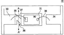
图3a示出了依照本发明一较佳实施例的一种发光二极管电路板的布线图。请参考图3a,在该较佳实施例中,发光二极管90焊粘于发光二极管电路板30,发光二极管电路板30包括:固晶区31、第一焊垫33、第二焊垫34与连接部35。发光二极管90封装工艺的固晶工艺中,固晶区31的表面将涂布一层绝缘胶以粘合发光二极管90,在接下来的焊线工艺中,焊线37的一端焊接于例如发光二极管90的负电极,而焊线37的另一端焊接第一焊垫33上,以使发光二极管90的负电极电性耦接于第一焊垫33。另一方面,另一焊线38的一端焊接于发光二极管90的正电极,而该焊线38的另一端焊接第二焊垫34上,以使发光二极管90的正电极电性耦接于第二焊垫34。而连接部35电性耦接于固晶区31与第一焊垫33。两个三角形挖空部分位于连接部35的外缘,由于该两个三角形挖空部分呈凹槽状,故当绝缘胶往第一焊垫33流动时,绝缘胶将停留在该三角形挖空部分中而不会流至第一焊垫33上,因此能有效地避免绝缘胶阻碍焊线的焊接的情形。Fig. 3a shows a wiring diagram of an LED circuit board according to a preferred embodiment of the present invention. Please refer to Fig. 3 a, in this preferred embodiment, light-emitting
此外,在后续的压模工艺中,连接部35的三角形挖空部分的结构可增加封胶材料与发光二极管电路板30的接触面积而提高两者间的结合力,如此,可提高发光二极管电路板30与封胶材料的密着度。In addition, in the subsequent compression molding process, the structure of the triangular hollow part of the
故,较佳实施例的发光二极管电路板30可有效地防止绝缘胶的溢流并提高封装工艺的可靠度。Therefore, the
图3b示出了沿着图3a的线AA’的发光二极管电路板的截面图。请同时参考图3a与图3b,该连接部35的三角形挖空部分36呈凹槽状,故当绝缘胶往第一焊垫33流动时,绝缘胶将停留在该三角形挖空部分36中而不会流至第一焊垫33上,因此能有效地避免绝缘胶阻碍焊线的焊接的情形。Fig. 3b shows a cross-sectional view of the LED circuit board along line AA' of Fig. 3a. Please refer to FIG. 3a and FIG. 3b at the same time, the triangular hollowed out
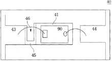
图4示出了依照本发明一较佳实施例的另一种发光二极管电路板的布线图。请参考图4,发光二极管90焊粘于电路板40,发光二极管电路板40包括:固晶区41、第一焊垫43、第二焊垫44与连接部45。发光二极管电路板40相异于发光二极管电路板30之处在于:连接部45具有位于其外缘的槽形挖空部分46,挖空部分46呈凹槽状,绝缘胶将停留在该槽形挖空部分46中而不会流至第一焊垫43上。Fig. 4 shows a wiring diagram of another LED circuit board according to a preferred embodiment of the present invention. Please refer to FIG. 4 , the
图5示出了依照本发明一较佳实施例的再一种发光二极管电路板的布线图。请参考图5,发光二极管90焊粘于发光二极管电路板50,发光二极管电路板50包括:固晶区51、第一焊垫53、第二焊垫54与连接部55。发光二极管电路板50相异于电路板30之处在于:连接部55具有位于其中心的矩形挖空部分56,该矩形挖空部分56呈凹槽状,绝缘胶将停留在该矩形挖空部分56中而不会流至第一焊垫53上。Fig. 5 shows a wiring diagram of another LED circuit board according to a preferred embodiment of the present invention. Please refer to FIG. 5 , the
图6示出了依照本发明另一较佳实施例的一种发光二极管电路板的布线图。请参考图6,在该较佳实施例中,发光二极管90a、90b焊粘于发光二极管电路板60,发光二极管电路板60包括:固晶区61a、61b,二第一焊垫63a、63b,二第二焊垫64a、64b,连接部65a、65b与导通孔67、69。同样地,在发光二极管90a、90b封装工艺的固晶工艺中,固晶区61a、61b的表面将涂布一层绝缘胶以分别粘合发光二极管90a、90b。在接下来的焊线工艺中,焊线的一端焊接于发光二极管90a的电极而焊线的另一端焊接第一焊垫63a上,并且另一焊线的一端焊接于发光二极管90b的电极而该焊线的另一端焊接第一焊垫63b上,以使发光二极管90a、90b的负电极分别电性耦接于二第一焊垫63a、63b,并且二第一焊垫63a、63b通过导通孔67、69而耦接于发光二极管电路板60的内部电路层。该处发光二极管电路板60是以包括两个导通孔67、69为例,然而发光二极管电路板60上也可包括更多的导通孔,端视工艺上的需求。而连接部65a电性耦接于固晶区61a与第一焊垫63a,并且连接部65b电性耦接于固晶区61b与第一焊垫63b。连接部65a、65b的三角形挖空部分66皆位于其外缘,由于该两个三角形挖空部分66呈凹槽状,故当绝缘胶往焊垫63a、63b流动时,绝缘胶将流至该三角形挖空部分66中而不会流至焊垫63a、63b上,因此能有效避免绝缘胶阻碍焊线的焊接的情形发生。另外,发光二极管电路板60还包括二第二焊垫64a、64b,各第二焊垫64a、64b耦接于各发光二极管90a、90b的另一电极,各第二焊垫64a、64b分别通过各导通孔69、67而耦接于发光二极管电路板60的内部电路层。Fig. 6 shows a wiring diagram of an LED circuit board according to another preferred embodiment of the present invention. Please refer to FIG. 6, in this preferred embodiment, the LEDs 90a, 90b are welded to the LED circuit board 60, and the LED circuit board 60 includes: solid crystal regions 61a, 61b, two first welding pads 63a, 63b, Two second pads 64a, 64b, connecting portions 65a, 65b and via holes 67, 69. Similarly, in the die-bonding process of the packaging process of the light-emitting diodes 90a and 90b, the surface of the die-bonding regions 61a and 61b will be coated with a layer of insulating glue to bond the light-emitting diodes 90a and 90b respectively. In the following wire bonding process, one end of the bonding wire is soldered to the electrode of the LED 90a and the other end of the bonding wire is soldered to the first pad 63a, and one end of the other bonding wire is soldered to the electrode of the LED 90b and the other end of the bonding wire is soldered to the electrode of the LED 90b. The other end of the welding wire is welded on the first welding pad 63b, so that the negative electrodes of the LEDs 90a, 90b are electrically coupled to the two first welding pads 63a, 63b respectively, and the two first welding pads 63a, 63b are connected The holes 67 , 69 are coupled to the inner circuit layer of the LED circuit board 60 . Here, the LED circuit board 60 includes two via holes 67 , 69 as an example, however, the LED circuit board 60 may also include more via holes, depending on the technical requirements. The connecting portion 65a is electrically coupled to the die-bonding area 61a and the first pad 63a, and the connecting portion 65b is electrically coupled to the die-bonding area 61b and the first pad 63b. The triangular hollowed-out parts 66 of the connecting parts 65a, 65b are all located on their outer edges. Since the two triangular hollowed-out parts 66 are in the shape of grooves, when the insulating glue flows to the welding pads 63a, 63b, the insulating glue will flow to the solder pads 63a, 63b. The triangular hollowed out portion 66 will not flow onto the welding pads 63a, 63b, thus effectively preventing the insulating glue from hindering the welding of the welding wires. In addition, the light-emitting diode circuit board 60 also includes two second welding pads 64a, 64b, each second welding pad 64a, 64b is coupled to the other electrode of each light-emitting diode 90a, 90b, and each second welding pad 64a, 64b passes through Each via hole 69 , 67 is coupled to the inner circuit layer of the LED circuit board 60 .
在封装工艺中,采用发光二极管电路板60不但能有效避免绝缘胶阻碍焊线的焊接的情形,另一方面,由于发光二极管90a、90b可共用导通孔67、69,故可减少导通孔67、69占据的发光二极管电路板60面积,以提高发光二极管电路板60上可设置发光二极管的数量。此外,由于本实施例采用先进的激光技术制作导通孔67、69,缩小导通孔67、69的直径,因此导通孔67、69占据的发光二极管电路板60面积可进一步有效地减少。In the packaging process, the use of the LED circuit board 60 can not only effectively avoid the situation that the insulating glue hinders the soldering of the welding wires, but on the other hand, since the LEDs 90a and 90b can share the via holes 67 and 69, the via holes can be reduced. The area of the light emitting diode circuit board 60 occupied by 67 and 69 is to increase the number of light emitting diodes that can be arranged on the light emitting diode circuit board 60 . In addition, since this embodiment adopts advanced laser technology to make the via holes 67, 69 and reduce the diameter of the via holes 67, 69, the area of the LED circuit board 60 occupied by the via holes 67, 69 can be further effectively reduced.
发光二极管电路板60将在切割工艺中被分割为两片电路板70(在图7中示出),以进行后续的封装测试。The LED circuit board 60 will be divided into two circuit boards 70 (shown in FIG. 7 ) in the dicing process for subsequent packaging and testing.
图7示出了依照本发明再一较佳实施例的一种发光二极管电路板的布线图。请参考图7。发光二极管90焊粘于发光二极管电路板70,发光二极管电路板70包括固晶区71、第一焊垫73、第二焊垫74与连接部75。此外,发光二极管电路板70可选择性地设置一稳压器基座76,用以耦接一稳压器而降低电磁干扰。Fig. 7 shows a wiring diagram of an LED circuit board according to yet another preferred embodiment of the present invention. Please refer to Figure 7. The
发光二极管电路板60、70的连接部65a、65b与75除了具有三角形挖空部分66、77外,也可选择性地具有位于连接部外缘的槽状挖空部分及/或位于其中心的挖空部分。然需注意的是,本发明的连接部65a、65b的结构并不限于上述实施例所述的结构,本发明所属的技术领域的技术人员可改变连接部的挖空部分的形状与位置,而仍不脱离本发明的精神与范围。The connecting
由上述本发明较佳实施例可知,应用本发明的发光二极管电路板具有下列优点:一、可避免绝缘胶溢流;二、提高单一电路板上发光二极管的数量;三、增加电路板与封胶材料的密着度;四、增加封装工艺可靠度;五、提高封装产能。It can be seen from the above-mentioned preferred embodiments of the present invention that the light-emitting diode circuit board of the present invention has the following advantages: 1. It can avoid the overflow of insulating glue; 2. Increase the number of light-emitting diodes on a single circuit board; 3. Increase the number of circuit boards and packaging. Fourth, increase the reliability of the packaging process; fifth, increase the packaging production capacity.
虽然本发明已以一较佳实施例揭露如上,然其并非用以限定本发明,任何熟悉本领域的技术人员,在不脱离本发明的精神和范围内,当可作各种的更动与润饰,因此本发明的保护范围当视后附的权利要求所界定者为准。Although the present invention has been disclosed above with a preferred embodiment, it is not intended to limit the present invention. Any person skilled in the art may make various modifications and changes without departing from the spirit and scope of the present invention. Modification, therefore, the scope of protection of the present invention shall prevail as defined by the appended claims.
Claims (5)
Priority Applications (1)
| Application Number | Priority Date | Filing Date | Title |
|---|---|---|---|
| CN2008101791226ACN101740675B (en) | 2008-11-25 | 2008-11-25 | LED circuit board |
Applications Claiming Priority (1)
| Application Number | Priority Date | Filing Date | Title |
|---|---|---|---|
| CN2008101791226ACN101740675B (en) | 2008-11-25 | 2008-11-25 | LED circuit board |
Publications (2)
| Publication Number | Publication Date |
|---|---|
| CN101740675A CN101740675A (en) | 2010-06-16 |
| CN101740675Btrue CN101740675B (en) | 2012-02-29 |
Family
ID=42463821
Family Applications (1)
| Application Number | Title | Priority Date | Filing Date |
|---|---|---|---|
| CN2008101791226AExpired - Fee RelatedCN101740675B (en) | 2008-11-25 | 2008-11-25 | LED circuit board |
Country Status (1)
| Country | Link |
|---|---|
| CN (1) | CN101740675B (en) |
Families Citing this family (1)
| Publication number | Priority date | Publication date | Assignee | Title |
|---|---|---|---|---|
| CN116133235B (en)* | 2023-02-28 | 2025-02-14 | 苏州晶台光电有限公司 | MiniLED lamp bead and display structure of PCB type substrate |
Citations (5)
| Publication number | Priority date | Publication date | Assignee | Title |
|---|---|---|---|---|
| US6175152B1 (en)* | 1998-06-25 | 2001-01-16 | Citizen Watch Co., Ltd. | Semiconductor device |
| CN1485929A (en)* | 2002-09-24 | 2004-03-31 | 友达光电股份有限公司 | Organic light-emitting diode |
| CN1667844A (en)* | 2004-03-08 | 2005-09-14 | 诠兴开发科技股份有限公司 | Packaging Structure of Side-light Color Light Emitting Diodes |
| CN1792125A (en)* | 2003-05-22 | 2006-06-21 | 电力波技术公司 | Circuit board assembly employing solder vent hole |
| CN1871710A (en)* | 2003-10-22 | 2006-11-29 | 克立公司 | Light-emitting chip package with electrical surface mount |
- 2008
- 2008-11-25CNCN2008101791226Apatent/CN101740675B/ennot_activeExpired - Fee Related
Patent Citations (5)
| Publication number | Priority date | Publication date | Assignee | Title |
|---|---|---|---|---|
| US6175152B1 (en)* | 1998-06-25 | 2001-01-16 | Citizen Watch Co., Ltd. | Semiconductor device |
| CN1485929A (en)* | 2002-09-24 | 2004-03-31 | 友达光电股份有限公司 | Organic light-emitting diode |
| CN1792125A (en)* | 2003-05-22 | 2006-06-21 | 电力波技术公司 | Circuit board assembly employing solder vent hole |
| CN1871710A (en)* | 2003-10-22 | 2006-11-29 | 克立公司 | Light-emitting chip package with electrical surface mount |
| CN1667844A (en)* | 2004-03-08 | 2005-09-14 | 诠兴开发科技股份有限公司 | Packaging Structure of Side-light Color Light Emitting Diodes |
Non-Patent Citations (1)
| Title |
|---|
| JP特开2006-310505A 2006.11.09 |
Also Published As
| Publication number | Publication date |
|---|---|
| CN101740675A (en) | 2010-06-16 |
Similar Documents
| Publication | Publication Date | Title |
|---|---|---|
| CN101447541B (en) | Semiconductor device with a plurality of transistors | |
| US8247833B2 (en) | LED package and manufacturing method thereof | |
| TWI419272B (en) | Semiconductor chip assembly with post/base heat spreader and signal post | |
| US8970053B2 (en) | Semiconductor package having light-emitting-diode solder-bonded on first and second conductive pads separated by at least 75 UM | |
| CN107170691A (en) | A kind of method for being superimposed on microbonding disk or carrying out automatic wedge bonding side by side | |
| TW201511347A (en) | Light-emitting diode package structure and manufacturing method thereof | |
| CN102881804B (en) | Substrate structure, semiconductor device array and semiconductor device having the same | |
| CN105990507A (en) | Side-illuminated light emitting diode structure and manufacturing method thereof | |
| WO2021027415A1 (en) | Led backlight module and display device | |
| TWI399845B (en) | Multi-chip stacked device without loop height and its manufacturing method | |
| TWI742991B (en) | Substrate structure and electronic device | |
| CN101877334A (en) | Semiconductor device with thermal gain | |
| CN202535631U (en) | Alumina ceramic circuit board with metal pillars and its packaging structure | |
| TWI384591B (en) | LED circuit board | |
| CN101740675B (en) | LED circuit board | |
| CN102117801B (en) | Manufacturing method of high-power light-emitting diode module structure | |
| JP2005051184A (en) | Printed wiring board, lighting device, and printed wiring board manufacturing method | |
| CN207068923U (en) | A kind of novel full color LED light source encapsulating structure and application | |
| JP5912471B2 (en) | Semiconductor device | |
| TW202416815A (en) | Display panel | |
| CN206532797U (en) | Light emitting element | |
| CN100514686C (en) | LED packaging structure | |
| CN221687534U (en) | Light emitting device package frame | |
| KR20050019664A (en) | Semiconductor package having solder balls | |
| TWI812124B (en) | Electronic module and carrier structure thereof and manufacturing method thereof |
Legal Events
| Date | Code | Title | Description |
|---|---|---|---|
| C06 | Publication | ||
| PB01 | Publication | ||
| C10 | Entry into substantive examination | ||
| SE01 | Entry into force of request for substantive examination | ||
| C14 | Grant of patent or utility model | ||
| GR01 | Patent grant | ||
| CF01 | Termination of patent right due to non-payment of annual fee | Granted publication date:20120229 Termination date:20141125 | |
| EXPY | Termination of patent right or utility model |