CN101738179A - Inductive coupling-based anchoring self-lifting profile monitoring buoy - Google Patents
Inductive coupling-based anchoring self-lifting profile monitoring buoyDownload PDFInfo
- Publication number
- CN101738179A CN101738179ACN200910154122ACN200910154122ACN101738179ACN 101738179 ACN101738179 ACN 101738179ACN 200910154122 ACN200910154122 ACN 200910154122ACN 200910154122 ACN200910154122 ACN 200910154122ACN 101738179 ACN101738179 ACN 101738179A
- Authority
- CN
- China
- Prior art keywords
- pin
- capacitor
- voltage
- resistor
- multiplication
- Prior art date
- Legal status (The legal status is an assumption and is not a legal conclusion. Google has not performed a legal analysis and makes no representation as to the accuracy of the status listed.)
- Granted
Links
- 230000008878couplingEffects0.000titleclaimsabstractdescription64
- 238000010168coupling processMethods0.000titleclaimsabstractdescription64
- 238000005859coupling reactionMethods0.000titleclaimsabstractdescription64
- 238000012544monitoring processMethods0.000titleclaimsabstractdescription42
- 238000004873anchoringMethods0.000titleclaims2
- 230000001939inductive effectEffects0.000titleabstractdescription6
- 238000004891communicationMethods0.000claimsabstractdescription35
- 230000005540biological transmissionEffects0.000claimsabstractdescription27
- 239000003990capacitorSubstances0.000claimsdescription265
- 238000002955isolationMethods0.000claimsdescription33
- 238000012546transferMethods0.000claimsdescription9
- 101000608720Helianthus annuus 10 kDa late embryogenesis abundant proteinProteins0.000claimsdescription6
- XLYOFNOQVPJJNP-UHFFFAOYSA-NwaterSubstancesOXLYOFNOQVPJJNP-UHFFFAOYSA-N0.000claimsdescription5
- 230000033228biological regulationEffects0.000claimsdescription2
- 238000001914filtrationMethods0.000claims16
- TVEXGJYMHHTVKP-UHFFFAOYSA-N6-oxabicyclo[3.2.1]oct-3-en-7-oneChemical compoundC1C2C(=O)OC1C=CC2TVEXGJYMHHTVKP-UHFFFAOYSA-N0.000claims1
- 230000006698inductionEffects0.000claims1
- 230000007812deficiencyEffects0.000abstract1
- 238000006243chemical reactionMethods0.000description41
- 238000007599dischargingMethods0.000description17
- 238000010586diagramMethods0.000description15
- 238000001514detection methodMethods0.000description14
- 238000000034methodMethods0.000description10
- 238000013500data storageMethods0.000description7
- 230000008054signal transmissionEffects0.000description5
- 230000007774longtermEffects0.000description3
- 230000008569processEffects0.000description3
- 230000003321amplificationEffects0.000description2
- 238000013461designMethods0.000description2
- 238000005516engineering processMethods0.000description2
- 238000007667floatingMethods0.000description2
- 238000003199nucleic acid amplification methodMethods0.000description2
- 230000003287optical effectEffects0.000description2
- 241001536374Indicator indicatorSpecies0.000description1
- 230000001174ascending effectEffects0.000description1
- 230000008859changeEffects0.000description1
- 230000000295complement effectEffects0.000description1
- 230000005674electromagnetic inductionEffects0.000description1
- 238000011160researchMethods0.000description1
- 239000000523sampleSubstances0.000description1
- 238000004804windingMethods0.000description1
Images


Landscapes
- Arrangements For Transmission Of Measured Signals (AREA)
Abstract
Translated fromChinese
Description
Translated fromChinese技术领域technical field
本发明属于水下无线通信技术领域,具体涉及一种基于感应耦合的锚泊自升降剖面监测浮标。The invention belongs to the technical field of underwater wireless communication, and in particular relates to a mooring self-elevating profile monitoring buoy based on inductive coupling.
背景技术Background technique
锚泊自升降剖面监测浮标同时具备锚泊浮标的长期定点特性和漂流式剖面监测浮标的可自动升降特性,可以获取特定研究海域的定点的、长期的、高垂直分辨率的序列垂直剖面监测数据,是近些年来发展起来的一种先进的海洋监测浮标。该类浮标通常采用两点系留式设计,即上端浮标牵拉,下端锚碇,剖面仪在浮标与锚碇间往复升降运动以采集剖面监测数据,剖面仪获取的监测数据借助某种通信方式传输至浮标体后,再由浮标体利用数传电台或通讯卫星发送至岸基数据中心。剖面仪与浮标体之间的通信方式若采用有线方式,则由于剖面仪的往复升降运动导致通信距离不断变化,不仅使得传输线路设计困难,同时通信的可靠性、剖面仪的安全性也难以保障。若采用无线方式,则在水下无线通信方式中,水声通信具有传输距离远、传输率高等一系列优点,但其成本过高,同时功耗较高,考虑到剖面仪的自容式供电特性,无法满足长期观测要求;水下激光通讯通信距离远、传输率较高,但结构复杂、造价高,同时通信的方向性要求高;水下LED光学通讯造价低、功耗低、传输距离较远、但同样存在方向性要求过高问题,若无相应装置保证其探头在较小的范围内对准,则通讯性能将大幅下降甚至通讯中断。The mooring self-elevating profile monitoring buoy has both the long-term fixed-point characteristics of the mooring buoy and the automatic lifting characteristics of the drifting profile monitoring buoy, and can obtain fixed-point, long-term, high vertical resolution serial vertical profile monitoring data in specific research sea areas. An advanced marine monitoring buoy developed in recent years. This type of buoy usually adopts a two-point mooring design, that is, the upper end is pulled by the buoy, and the lower end is anchored. The profiler moves back and forth between the buoy and the anchorage to collect profile monitoring data. The monitoring data obtained by the profiler is obtained by a certain communication method. After being transmitted to the buoy body, the buoy body uses a digital transmission station or a communication satellite to send it to the shore-based data center. If the communication method between the profiler and the buoy adopts a wired method, the communication distance is constantly changing due to the reciprocating lifting movement of the profiler, which not only makes the design of the transmission line difficult, but also difficult to guarantee the reliability of communication and the safety of the profiler . If the wireless method is adopted, in the underwater wireless communication method, the underwater acoustic communication has a series of advantages such as long transmission distance and high transmission rate, but its cost is too high, and the power consumption is high at the same time. Considering the self-contained power supply of the profiler characteristics, unable to meet long-term observation requirements; underwater laser communication has long communication distance and high transmission rate, but complex structure, high cost, and high communication directionality requirements; underwater LED optical communication has low cost, low power consumption, and long transmission distance It is far away, but there is also the problem of high directionality requirements. If there is no corresponding device to ensure that the probe is aligned within a small range, the communication performance will be greatly reduced or even communication will be interrupted.
发明内容Contents of the invention
本发明的目的在于提拱一种基于感应耦合的锚泊自升降剖面监测浮标。该浮标可以在剖面仪上浮或下降过程中实现剖面监测数据的水下采集与自容式存储,在浮标体上实现剖面监测数据的存储以及数传电台或卫星远程转发,在剖面仪上浮至浮标体底部时实现剖面监测数据在剖面仪与浮标体之间的近距离非接触式无线传输,满足剖面仪与浮标体间数据存储与传输的低成本、低功耗和高可靠性要求。The purpose of the present invention is to provide a self-elevating profile monitoring buoy for mooring based on inductive coupling. The buoy can realize the underwater collection and self-contained storage of the profile monitoring data during the floating or descending process of the profiler. The storage of the profile monitoring data and the remote transmission of the data transmission station or satellite can be realized on the buoy body. The near-distance non-contact wireless transmission of profile monitoring data between the profiler and the buoy body is realized at the bottom of the body, which meets the requirements of low cost, low power consumption and high reliability for data storage and transmission between the profiler and the buoy body.
为解决上述技术问题,本发明所采取的具体技术方案是:In order to solve the problems of the technologies described above, the concrete technical scheme that the present invention takes is:
基于感应耦合的锚泊自升降剖面监测浮标包括天线、浮标体、浮标体仪器仓、通讯收发模块、水下剖面仪、单向锁定开关、剖面仪传感器、系留缆和配重块。The mooring self-elevating profile monitoring buoy based on inductive coupling includes antenna, buoy body, buoy body instrument compartment, communication transceiver module, underwater profiler, one-way locking switch, profiler sensor, mooring cable and counterweight.
浮标体的顶部设置有天线,浮标体底部设置有下支架,下支架的底部与系留缆的一端连接,系留缆的另一端与配重块连接,系留缆上设置有单向锁定装置,单向锁定装置与水下剖面仪的侧壁固定设置,剖面仪传感器设置在水下剖面仪内腔;The top of the buoy body is provided with an antenna, the bottom of the buoy body is provided with a lower bracket, the bottom of the lower bracket is connected to one end of the mooring cable, the other end of the mooring cable is connected to the counterweight, and the mooring cable is provided with a one-way locking device , the one-way locking device is fixedly arranged with the side wall of the underwater profiler, and the profiler sensor is arranged in the inner cavity of the underwater profiler;
浮标体仪器仓设置在浮标体内,通讯收发模块设置在浮标体仪器仓内。浮标体仪器仓内还设置有浮标数据转发模块和耦合信号接收模块,通讯收发模块通过串口与浮标数据转发模块信号连接,耦合信号接收模块通过串口与浮标数据转发模块信号连接;The instrument compartment of the buoy body is arranged in the body of the buoy, and the communication transceiver module is arranged in the instrument compartment of the buoy body. The buoy body instrument compartment is also equipped with a buoy data forwarding module and a coupling signal receiving module. The communication transceiver module is connected to the buoy data forwarding module through a serial port, and the coupling signal receiving module is connected to the buoy data forwarding module through a serial port.
系留缆上还套接有耦合信号接收线圈和耦合信号发送线圈,耦合信号接收线圈设置在下支架上并与耦合信号接收模块信号连接;耦合信号发送线圈与剖面仪内腔中的耦合信号发送模块信号连接,耦合信号发送模块与水下数据采集与存储模块信号连接,水下数据采集与存储模块与剖面仪传感器信号连接。The mooring cable is also sleeved with a coupling signal receiving coil and a coupling signal sending coil. The coupling signal receiving coil is arranged on the lower bracket and connected with the coupling signal receiving module; the coupling signal sending coil is connected to the coupling signal sending module in the inner cavity of the profiler. Signal connection and coupling The signal sending module is connected to the underwater data acquisition and storage module, and the underwater data acquisition and storage module is connected to the profiler sensor.
所述的水下数据采集与存储模块包括核心板和底板,核心板和底板之间通过核心板总线连接;所述的底板包括数据存储模块、剖面仪传感器数据接口模块、监测数据中转远程传输接口模块、控制量接口模块以及调试接口模块。The underwater data acquisition and storage module includes a core board and a bottom board, and the core board and the bottom board are connected by a core board bus; the bottom board includes a data storage module, a profiler sensor data interface module, and a monitoring data transfer remote transmission interface module, control quantity interface module and debugging interface module.
数据存储模块包括第一高频滤波电容C9、第二高频滤波电容C10、第三高频滤波电容C12、第四高频滤波电容C13、第一低频滤波电解电容C8、第二低频滤波电解电容C11、第一保险丝F1、第二保险丝F2、双排USB插头连接器CN2。The data storage module includes a first high-frequency filter capacitor C9, a second high-frequency filter capacitor C10, a third high-frequency filter capacitor C12, a fourth high-frequency filter capacitor C13, a first low-frequency filter electrolytic capacitor C8, and a second low-frequency filter electrolytic capacitor C11, a first fuse F1, a second fuse F2, and a double-row USB plug connector CN2.
第二高频滤波电容C10的一端和第一保险丝F1的一端接5V电源,第一保险丝F1的另一端、第一高频滤波电容C9的一端、第一低频滤波电解电容C8的正极与双排USB插头连接器CN2的1脚连接;第二高频滤波电容C10的另一端、第一高频滤波电容C9的另一端和第一低频滤波电解电容C8的负极均接地;One end of the second high-frequency filter capacitor C10 and one end of the first fuse F1 are connected to a 5V power supply, the other end of the first fuse F1, one end of the first high-frequency filter capacitor C9, the positive electrode of the first low-frequency filter electrolytic capacitor C8 and the
第四高频滤波电容C13的一端和第二保险丝F2的一端接5V电源,第二保险丝F2的另一端、第三高频滤波电容C12的一端、第二低频滤波电解电容C11的正极与双排USB插头连接器CN2的5脚连接;第四高频滤波电容C13的另一端、第三高频滤波电容C12的另一端和第二低频滤波电解电容C11的负极均接地;One end of the fourth high-frequency filter capacitor C13 and one end of the second fuse F2 are connected to a 5V power supply, the other end of the second fuse F2, one end of the third high-frequency filter capacitor C12, the positive electrode of the second low-frequency filter electrolytic capacitor C11 and the double row The 5-pin connection of the USB plug connector CN2; the other end of the fourth high frequency filter capacitor C13, the other end of the third high frequency filter capacitor C12 and the negative pole of the second low frequency filter electrolytic capacitor C11 are all grounded;
底板剖面仪传感器数据接口模块包括第一电平转换芯片U3、第二电平转换芯片U4、第一倍压电解电容C20、第二倍压电解电容C21、第三倍压电解电容C22、第四倍压电解电容C23、第五倍压电解电容C24、第六倍压电解电容C25、第七倍压电解电容C26、第八倍压电解电容C27、第九倍压电解电容C28、第十倍压电解电容C29;第一倍压电解电容C20的正极与第一电平转换芯片U3的1脚连接,负极与第一电平转换芯片U3的3脚连接,第二倍压电解电容C21的正极与第一电平转换芯片U3的4脚连接,负极与第二电平转换芯片U3的5脚连接,第三倍压电解电容C22的负极、第四倍压电解电容C23的正极和第一电平转换芯片U3的16脚接5V电源,第三倍压电解电容C22的正极与第一电平转换芯片U3的2脚连接,第四倍压电解电容C23的负极接地;第五倍压电解电容C24负极与第一电平转换芯片U3的6脚连接,正极接地;The sensor data interface module of the base plate profiler includes the first level conversion chip U3, the second level conversion chip U4, the first voltage doubler electrolytic capacitor C20, the second voltage doubler electrolytic capacitor C21, and the third voltage doubler electrolytic capacitor C22 , the fourth double voltage electrolytic capacitor C23, the fifth double voltage electrolytic capacitor C24, the sixth double voltage electrolytic capacitor C25, the seventh double voltage electrolytic capacitor C26, the eighth double voltage electrolytic capacitor C27, the ninth double voltage The electrolytic capacitor C28, the tenth voltage multiplier electrolytic capacitor C29; the positive pole of the first voltage multiplier electrolytic capacitor C20 is connected to
第六倍压电解电容C25的正极与第二电平转换芯片U4的1脚连接,负极与第一电平转换芯片U3的3脚连接,第七倍压电解电容C21的正极与第一电平转换芯片U4的4脚连接,负极与第二电平转换芯片U4的5脚连接,第八倍压电解电容C27的负极、第九倍压电解电容C28的正极和第二电平转换芯片U4的16脚接5V电源,第八倍压电解电容C27的正极与第二电平转换芯片U4的2脚连接,第九倍压电解电容C28的负极接地;第十倍压电解电容C29负极与第二电平转换芯片U4的6脚连接,正极接地;The positive pole of the sixth voltage multiplier electrolytic capacitor C25 is connected to
监测数据中转远程传输接口模块包括第三电平转换芯片U2,第十一倍压电解电容C15、第十二倍压电解电容C16、第十三倍压电解电容C17、第十四倍压电解电容C18、第十五倍压电解电容C19;第十一倍压电解电容C15正极与第三电平转换芯片U2的1脚连接,负极与第三电平转换芯片U2的3脚连接,第十二倍压电解电容C16正极与第三电平转换芯片U2的4脚连接,负极与第三电平转换芯片U2的5脚连接,第十三倍压电解电容C17负极、第十四倍压电解电容C18正极和第三电平转换芯片U2的16脚与5V电源连接;第十三倍压电解电容C17正极与第三电平转换芯片U2的2脚连接,第十四倍压电解电容C18负极接地,第十五倍压电解电容C19负极与第三电平转换芯片U2的6脚连接,正极接地;The monitoring data transfer remote transmission interface module includes the third level conversion chip U2, the eleventh multiplier electrolytic capacitor C15, the twelfth multiplier electrolytic capacitor C16, the thirteenth multiplier electrolytic capacitor C17, the fourteenth multiplier The piezoelectric capacitor C18, the fifteenth-times pressure electrolytic capacitor C19; the positive electrode of the eleventh-times pressure electrolytic capacitor C15 is connected to
控制量接口模块包括状态指示灯供电调压器U5、第五高频滤波电容C3、第三低频滤波电解电容C4、第一IO状态指示灯DS2、第二IO状态指示灯DS3、第三IO状态指示灯DS4、第四IO状态指示灯DS5、第五IO状态指示灯DS6、第六IO状态指示灯DS7、第七IO状态指示灯DS8、第八IO状态指示灯DS8、第九IO状态指示灯DS10、第一限流电阻R7、第二限流电阻R8、第三限流电阻R9、第四限流电阻R10、第五限流电阻R11、第六限流电阻R12、第七限流电阻R13、第八限流电阻R14、第九限流电阻R15;第五高频滤波电容C3一端、第三低频滤波电解电容C4正极与状态指示灯供电调压器U5的输出端连接;第五高频滤波电容C3另一端、第三低频滤波电解电容C4负极、状态指示灯供电调压器U5的接地端接接地;状态指示灯供电调压器U5的输入端接5V电源;The control quantity interface module includes a status indicator power supply voltage regulator U5, a fifth high-frequency filter capacitor C3, a third low-frequency filter electrolytic capacitor C4, a first IO status indicator DS2, a second IO status indicator DS3, and a third IO status indicator Indicator DS4, fourth IO status indicator DS5, fifth IO status indicator DS6, sixth IO status indicator DS7, seventh IO status indicator DS8, eighth IO status indicator DS8, ninth IO status indicator DS10, first current limiting resistor R7, second current limiting resistor R8, third current limiting resistor R9, fourth current limiting resistor R10, fifth current limiting resistor R11, sixth current limiting resistor R12, seventh current limiting resistor R13 , the eighth current-limiting resistor R14, the ninth current-limiting resistor R15; one end of the fifth high-frequency filter capacitor C3, the positive pole of the third low-frequency filter electrolytic capacitor C4 is connected to the output end of the status indicator power supply voltage regulator U5; the fifth high-frequency The other end of the filter capacitor C3, the negative pole of the third low-frequency filter electrolytic capacitor C4, and the ground terminal of the status indicator power supply voltage regulator U5 are connected to ground; the input terminal of the status indicator power supply voltage regulator U5 is connected to a 5V power supply;
第一限流电阻R7一端、第二限流电阻R8一端、第三限流电阻R9一端、第四限流电阻R10一端、第五限流电阻R11一端、第六限流电阻R12一端、第七限流电阻R13一端、第八限流电阻R14一端和第九限流电阻R15一端并联后接状态指示灯供电调压器U5的输出端;第一限流电阻R7另一端接第一IO状态指示灯DS2的正极,第二限流电阻R8另一端接第二IO状态指示灯DS3的正极,第三限流电阻R9另一端接第三IO状态指示灯DS4的正极,第四限流电阻R10另一端接第四IO状态指示灯DS5的正极,第五限流电阻R11另一端接第五IO状态指示灯DS6的正极,第六限流电阻R12另一端接第六IO状态指示灯DS7的正极,第七限流电阻R13另一端接第七IO状态指示灯DS8的正极,第八限流电阻R14另一端接第八IO状态指示灯DS9的正极,第九限流电阻R15另一端接第九IO状态指示灯DS10的正极;One end of the first current-limiting resistor R7, one end of the second current-limiting resistor R8, one end of the third current-limiting resistor R9, one end of the fourth current-limiting resistor R10, one end of the fifth current-limiting resistor R11, one end of the sixth current-limiting resistor R12, one end of the seventh One end of the current-limiting resistor R13, one end of the eighth current-limiting resistor R14 and one end of the ninth current-limiting resistor R15 are connected in parallel to the output end of the status indicator power supply voltage regulator U5; the other end of the first current-limiting resistor R7 is connected to the first IO status indicator The positive pole of the lamp DS2, the other end of the second current-limiting resistor R8 is connected to the positive pole of the second IO status indicator DS3, the other end of the third current-limiting resistor R9 is connected to the positive pole of the third IO status indicator DS4, and the other end of the fourth current-limiting resistor R10 One end is connected to the positive pole of the fourth IO status indicator DS5, the other end of the fifth current limiting resistor R11 is connected to the positive pole of the fifth IO status indicator DS6, the other end of the sixth current limiting resistor R12 is connected to the positive pole of the sixth IO status indicator DS7, The other end of the seventh current limiting resistor R13 is connected to the positive pole of the seventh IO status indicator DS8, the other end of the eighth current limiting resistor R14 is connected to the positive pole of the eighth IO status indicator DS9, and the other end of the ninth current limiting resistor R15 is connected to the ninth IO The positive pole of the status indicator DS10;
调试接口模块包括网络隔离变压器U1、RJ45网络接头CN1、第一匹配电阻R1、第二匹配电阻R2、第三匹配电阻R3、第四匹配电阻R4、第六高频滤波电容C5、耐压电容C6和隔离电容C7;The debugging interface module includes network isolation transformer U1, RJ45 network connector CN1, first matching resistor R1, second matching resistor R2, third matching resistor R3, fourth matching resistor R4, sixth high-frequency filter capacitor C5, and withstand voltage capacitor C6 and isolation capacitor C7;
第一匹配电阻R1的一端、第二匹配电阻R2的一端、第三匹配电阻R3的一端和第四匹配电阻R4的一端与耐压电容C6一端连接,耐压电容C6另一端与隔离电容C7一端连接后接大地,隔离电容C7另一端接地,第一匹配电阻R1的另一端与网络隔离变压器U1的10脚连接,第二匹配电阻R2的另一端与网络隔离变压器U1的15脚连接,第三匹配电阻R3的另一端与RJ45网络接头CN1的4脚和5脚连接,第四匹配电阻R4的另一端与RJ45网络接头CN1的7脚和8脚连接,网络隔离变压器U1的16脚与RJ45网络接头CN1的1脚连接,网络隔离变压器U1的14脚与RJ45网络接头CN1的2脚连接,网络隔离变压器U1的11脚与RJ45网络接头CN1的3脚连接,网络隔离变压器U1的9脚与RJ45网络接头CN1的6脚连接,高频滤波电容C5的一端接网络隔离变压器U1的7脚,另一端接地;One end of the first matching resistor R1, one end of the second matching resistor R2, one end of the third matching resistor R3 and one end of the fourth matching resistor R4 are connected to one end of the withstand voltage capacitor C6, and the other end of the withstand voltage capacitor C6 is connected to one end of the isolation capacitor C7 Connect to the ground after connection, the other end of the isolation capacitor C7 is grounded, the other end of the first matching resistor R1 is connected to the 10-pin of the network isolation transformer U1, the other end of the second matching resistor R2 is connected to the 15-pin of the network isolation transformer U1, and the third The other end of the matching resistor R3 is connected to
所述的耦合信号发送模块由数据接口、调制电路、功放电路构成。数据接口通过串口与水下数据采集与存储模块信号连接,调制电路一端与数据接口信号连接,另一端与功放电路一端信号连接,功放电路一端与调制电路信号连接,另一端与耦合信号发送线圈连接。The coupling signal sending module is composed of a data interface, a modulation circuit and a power amplifier circuit. The data interface is connected to the signal of the underwater data acquisition and storage module through the serial port, one end of the modulation circuit is connected to the signal of the data interface, the other end is connected to the signal of one end of the power amplifier circuit, one end of the power amplifier circuit is connected to the signal of the modulation circuit, and the other end is connected to the coupling signal sending coil .
所述的耦合信号接收模块由放大电路、前端滤波电路、检波电路、后端滤波电路、数字信号还原电路和数据接口构成。其中,放大电路一端连接耦合信号接收线圈,另一端与前端滤波电路一端信号连接,前端滤波电路另一端与检波电路一端信号连接,检波电路另一端与后端滤波电路一端信号连接,后端滤波电路与数字信号还原电路一端信号连接,数字信号还原电路另一端连接数据接口。The coupling signal receiving module is composed of an amplifier circuit, a front-end filter circuit, a detection circuit, a back-end filter circuit, a digital signal restoration circuit and a data interface. Among them, one end of the amplification circuit is connected to the coupling signal receiving coil, the other end is connected to the signal at one end of the front-end filter circuit, the other end of the front-end filter circuit is connected to the signal at one end of the detection circuit, the other end of the detection circuit is connected to the signal at one end of the back-end filter circuit, and the back-end filter circuit One end of the digital signal restoration circuit is signal-connected, and the other end of the digital signal restoration circuit is connected to the data interface.
所述的发送线圈和接收线圈均采用Φ1.2mm漆包线绕制,线圈形状为圆形,直径7.5cm,匝数为10。Both the sending coil and the receiving coil are wound with Φ1.2mm enameled wire, the coil shape is circular, the diameter is 7.5cm, and the number of turns is 10.
所述的调制电路包括时基电路LM555,第一充放电电容C1、第二充放电电容C2,可调电阻R5、频率设置电阻R6、二极管D1和运算放大器LM318N;第一充放电电容C1的一端和时基电路LM555的1脚接地,第一充放电电容C1的另一端与时基电路LM555的5脚连接,二极管D1的阴极、时基电路LM555的6脚、时基电路LM555的2脚、频率设置电阻R6的一端与第二充放电电容C2的一端连接,第二充放电电容C2的另一端接地,频率设置电阻R6的另一端、二极管D1的阳极和时基电路LM555的7脚与可调电阻R5一端连接,可调电阻R5另一端和时基电路LM555的8脚接5V电源,可调电阻R5的可调端与时基电路LM555的7脚连接;时基电路LM555的3脚与运算放大器LM318N的同相输入端连接,运算放大器LM318N的反相输入端与运算放大器LM318N的输出端连接。The modulation circuit includes a time base circuit LM555, a first charging and discharging capacitor C1, a second charging and discharging capacitor C2, an adjustable resistor R5, a frequency setting resistor R6, a diode D1 and an operational amplifier LM318N; one end of the first charging and discharging capacitor C1 Connect
所述的前端滤波电路6-2包括第一截止频率设置电容C6、第二截止频率设置电容C7,第一截止频率设置电阻R10、第二截止频率设置电阻R11、第一负反馈电阻R12、第二负反馈电阻R13和运算放大器OP07CN;第二截止频率设置电阻R11一端、第一截止频率设置电容C6一端与第一截止频率设置电阻R10的一端连接,第二截止频率设置电阻R11另一端、第二截止频率设置电容C7一端与运算放大器OP07CN的同相输入端连接,第二截止频率设置电容C7另一端接地,第一截止频率设置电容C6另一端、第二负反馈电阻R13一端与运算放大器OP07CN的输出端连接,第二负反馈电阻R13另一端、第一负反馈电阻R12一端与运算放大器OP07CN的反相输入端连接,第一负反馈电阻R12另一端接地;The front-end filter circuit 6-2 includes a first cut-off frequency setting capacitor C6, a second cut-off frequency setting capacitor C7, a first cut-off frequency setting resistor R10, a second cut-off frequency setting resistor R11, a first negative feedback resistor R12, and a first cut-off frequency setting resistor R11. Two negative feedback resistors R13 and operational amplifier OP07CN; one end of the second cutoff frequency setting resistor R11, one end of the first cutoff frequency setting capacitor C6 is connected to one end of the first cutoff frequency setting resistor R10, the other end of the second cutoff frequency setting resistor R11, the second cutoff frequency setting resistor R11 One end of the second cut-off frequency setting capacitor C7 is connected to the non-inverting input end of the operational amplifier OP07CN, the other end of the second cut-off frequency setting capacitor C7 is grounded, the other end of the first cut-off frequency setting capacitor C6, and one end of the second negative feedback resistor R13 are connected to the operational amplifier OP07CN. The output end is connected, the other end of the second negative feedback resistor R13, one end of the first negative feedback resistor R12 are connected to the inverting input end of the operational amplifier OP07CN, and the other end of the first negative feedback resistor R12 is grounded;
所述的检波电路包括整流二极管D4,第三充放电电容C8,充放电电阻R14,运算放大器LF351AN。整流二极管D4一端、第三充放电电容C8一端、充放电电阻R14一端与运算放大器LF351AN的同相输入端连接,第三充放电电容C8另一端和充放电电阻R14另一端接地,运算放大器LF351AN的反相输入端与运算放大器LF351AN的输出端连接。The detection circuit includes a rectifier diode D4, a third charging and discharging capacitor C8, a charging and discharging resistor R14, and an operational amplifier LF351AN. One end of the rectifier diode D4, one end of the third charge and discharge capacitor C8, and one end of the charge and discharge resistor R14 are connected to the non-inverting input end of the operational amplifier LF351AN, the other end of the third charge and discharge capacitor C8 and the other end of the charge and discharge resistor R14 are grounded, and the opposite end of the operational amplifier LF351AN The phase input terminal is connected with the output terminal of the operational amplifier LF351AN.
所述的数字信号还原电路包括滤波电解电容C12、第一偏置电阻R22、第二偏置电阻R23、第一上限电压分压电阻R19、第二上限电压分压电阻R20、第一下限电压分压电阻R24、第二下限电压分压电阻R25、第一上拉电阻R21、第二上拉电阻R26、电压比较器LM339AN和集成与非门SN74LS00N;The digital signal restoration circuit includes a filter electrolytic capacitor C12, a first bias resistor R22, a second bias resistor R23, a first upper limit voltage divider resistor R19, a second upper limit voltage divider resistor R20, a first lower limit voltage divider Piezoresistor R24, second lower limit voltage divider resistor R25, first pull-up resistor R21, second pull-up resistor R26, voltage comparator LM339AN and integrated NAND gate SN74LS00N;
第一偏置电阻R22一端、第二偏置电阻R23一端、电压比较器LM339AN的5脚和电压比较器LM339AN的7脚与滤波电容C12的负端连接,电压比较器LM339AN的4脚、第一上限电压分压电阻R19的一端与第二上限电压分压电阻R20的一端连接,第二上限电压分压电阻R20的另一端、电压比较器LM339AN的3脚和第一上拉电阻R21一端接+5V,电压比较器LM339AN的2脚、第一上拉电阻R21另一端、集成与非门SN74LS00N的2脚与集成与非门SN74LS00N的1脚连接,第一上限电压分压电阻R19的另一端接地;One end of the first bias resistor R22, one end of the second bias resistor R23,
电压比较器LM339AN的6脚、第一下限电压分压电阻R24的一端与第二下限电压分压电阻R25的一端连接,第二下限电压分压电阻R25的另一端、电压比较器LM339AN的3脚和第二上拉电阻R26一端接+5V,第二上拉电阻R26另一端、电压比较器LM339AN的1脚与集成与非门SN74LS00N的12脚连接,第一下限电压分压电阻R24的另一端接地,集成与非门SN74LS00N的5脚与11脚连接,集成与非门SN74LS00N的6脚与13脚连接;
本发明提出的锚泊自升降剖面监测浮标,其剖面监测数据的传输过程具有非接触特性,使得锚泊自升降监测浮标的剖面仪与浮标体可采用分离式设计,二者之间除系留缆外,无需添加额外的通信线路,既保证了数据通信的可靠性,同时也保障了监测浮标的安全性。此外,本发明提出的水下无线数据传输装置基于电磁感应原理,对于收、发线圈相对位置的方向性要求较低,可以在较大的空间角度范围内实现近距离非接触式无线传输,除此之外,该装置还具有成本低、功耗小等一系列优点,与水声通讯、水下光学通讯等背景技术相比,更加适合实现剖面仪与浮标体之间的近距离非接触式无线数据传输。The mooring self-elevating profile monitoring buoy proposed by the present invention has non-contact characteristics in the transmission process of its profile monitoring data, so that the profiler and the buoy body of the mooring self-elevating monitoring buoy can be designed separately, except for the mooring cable. , there is no need to add additional communication lines, which not only ensures the reliability of data communication, but also ensures the safety of the monitoring buoy. In addition, the underwater wireless data transmission device proposed by the present invention is based on the principle of electromagnetic induction, and has low requirements for the directionality of the relative positions of the receiving and transmitting coils, and can realize short-distance non-contact wireless transmission within a large spatial angle range. In addition, the device also has a series of advantages such as low cost and low power consumption. Compared with background technologies such as underwater acoustic communication and underwater optical communication, it is more suitable for realizing short-distance non-contact communication between the profiler and the buoy body. Wireless data transmission.
附图说明Description of drawings
图1为本发明结构示意图;Fig. 1 is a structural representation of the present invention;
图2为本发明中数据传输示意图;Fig. 2 is a schematic diagram of data transmission in the present invention;
图3为图2中水下数据采集与存储模块和浮标数据转发模块示意图;Fig. 3 is a schematic diagram of the underwater data acquisition and storage module and the buoy data forwarding module in Fig. 2;
图4为图3中核心板总线示意图;Fig. 4 is a schematic diagram of the core board bus in Fig. 3;
图5为图3中底板数据存储模块示意图;Fig. 5 is a schematic diagram of the data storage module of the backplane in Fig. 3;
图6为图3中底板剖面仪传感器数据接口模块示意图;Fig. 6 is a schematic diagram of the sensor data interface module of the floor profiler in Fig. 3;
图7为图3中监测数据中转远程传输接口模块示意图;Fig. 7 is a schematic diagram of the monitoring data transfer remote transmission interface module in Fig. 3;
图8为图3中控制量接口模块示意图;Fig. 8 is a schematic diagram of the control quantity interface module in Fig. 3;
图9为图3中调试接口模块示意图;Fig. 9 is a schematic diagram of the debugging interface module in Fig. 3;
图10为图2中的耦合信号发送模块结构示意图;Fig. 10 is a schematic structural diagram of the coupling signal sending module in Fig. 2;
图11为图2中的耦合信号接收模块结构示意图;Fig. 11 is a schematic structural diagram of the coupling signal receiving module in Fig. 2;
图12为图2中的发送线圈和接收线圈示意图;Fig. 12 is a schematic diagram of the transmitting coil and the receiving coil in Fig. 2;
图13为图10中的调制电路示意图;Fig. 13 is a schematic diagram of the modulation circuit in Fig. 10;
图14为图11中的前端滤波电路示意图;Fig. 14 is a schematic diagram of the front-end filter circuit in Fig. 11;
图15为图11中的检波电路示意图;Fig. 15 is a schematic diagram of the detection circuit in Fig. 11;
图16为图11中的数字信号还原电路示意图。FIG. 16 is a schematic diagram of the digital signal restoration circuit in FIG. 11 .
具体实施方式Detailed ways
下面结合附图对本发明作进一步的说明。The present invention will be further described below in conjunction with the accompanying drawings.
如图1所示(图中曲线为水面),基于感应耦合的锚泊自升降剖面监测浮标,包括天线1、浮标体2、浮标体仪器仓3、通讯收发模块4、水下剖面仪9、单向锁定开关10、剖面仪传感器13、系留缆14和配重块15。As shown in Figure 1 (the curve in the figure is the water surface), the mooring self-elevating profile monitoring buoy based on inductive coupling includes
浮标体2的顶部设置有天线1,浮标体2底部设置有下支架,下支架的底部与系留缆14的一端连接,系留缆14的另一端与配重块15连接,系留缆14上设置有单向锁定装置10,单向锁定装置10与水下剖面仪9的侧壁固定设置,剖面仪传感器13设置在水下剖面仪9内腔;The top of the
浮标体仪器仓3设置在浮标体2内,通讯收发模块4设置在浮标体仪器仓3内。浮标体仪器仓3内还设置有浮标数据转发模块5和耦合信号接收模块6,通讯收发模块4通过串口与浮标数据转发模块5信号连接,耦合信号接收模块6通过串口与浮标数据转发模块5信号连接;The buoy
系留缆14上还套接有耦合信号接收线圈7和耦合信号发送线圈8,耦合信号接收线圈7设置在下支架上并与耦合信号接收模块6信号连接;耦合信号发送线圈8与剖面仪9内腔中的耦合信号发送模块11信号连接,耦合信号发送模块11与水下数据采集与存储模块12信号连接,水下数据采集与存储模块12与剖面仪传感器13信号连接。The
天线1可以选用数传电台天线或卫星通讯天线,耦合信号接收模块6与耦合信号接收线圈7采用双芯水密电缆连接;耦合信号发送模块11与耦合信号发送线圈8也采用双芯水密电缆连接;水下数据采集与存储模块12与耦合信号发送模块11采用RS232串口连接。The
如图2所示,数据传输主要依靠水下数据采集与存储模块12、耦合信号发送模块11、耦合信号发送线圈8、耦合信号接收线圈7、耦合信号接收模块6以及浮标数据转发模块5。其中,水下数据采集与存储模块12与耦合信号发送模块11之间采用RS232串口相连接;耦合信号发送模块11与耦合信号发送线圈8之间可直接采用普通导线连接,耦合信号发送线圈8置于水下时需采用双芯水密导线;耦合信号接收线圈7与耦合信号接收模块6之间的连接方式与发送模块11、线圈8之间的连接方式类似;耦合信号接收模块6与浮标数据转发模块5之间采用RS232串口相连接。As shown in FIG. 2 , data transmission mainly relies on the underwater data acquisition and
如图3所示,水下数据采集与存储模块12包括核心板5-1和底板5-2,核心板5-1和底板5-2之间通过核心板总线5-3连接;所述的底板5-2包括数据存储模块5-2-1、剖面仪传感器数据接口模块5-2-2、监测数据中转远程传输接口模块5-2-3、控制量接口模块5-2-4以及调试接口模块5-2-5。其中,核心板5-1采用成都英创信息技术有限公司EM9160ARM9工控主板;核心板5-1与底板5-2之间采用核心板总线5-3相连接。As shown in Figure 3, the underwater data acquisition and
如图4所示,核心板总线5-3包含EM9160_CN1和EM9160_CN2两个针状双排插座。依据信号线间的相互逻辑关系以及实现的功能,可分为RJ45网络接口信号线(CN11-6)、USB接口信号线(CN17、8、23、24)、串口信号线(CN113-22、25、26、29-34)、GPIO接口信号线(CN110、12、35、36,CN28、33-36)以及扩展总线(CN23、7、9、10、12、13-24)。As shown in Figure 4, the core board bus 5-3 includes two pin-shaped double-row sockets EM9160_CN1 and EM9160_CN2. According to the mutual logical relationship between the signal lines and the functions realized, they can be divided into RJ45 network interface signal lines (CN11-6), USB interface signal lines (CN17, 8, 23, 24), serial port signal lines (CN113-22, 25 , 26, 29-34), GPIO interface signal lines (CN110, 12, 35, 36, CN28, 33-36) and expansion bus (CN23, 7, 9, 10, 12, 13-24).
核心板5-1以ARM9芯片AT91SAM9260为CPU,负责操作系统加载和系统初始化,借助核心板总线5-3实现核心板5-1与底板5-2之间的通讯、底板5-2各模块间的协调、剖面监测数据的采集与存储控制以及借助耦合信号发送模块11发送监测数据等功能。The core board 5-1 uses the ARM9 chip AT91SAM9260 as the CPU, is responsible for operating system loading and system initialization, and realizes the communication between the core board 5-1 and the base board 5-2 by means of the core board bus 5-3, and between the modules of the base board 5-2. The functions of coordination, collection and storage control of profile monitoring data, and sending monitoring data by means of coupling
如图5所示,数据存储模块5-2-1包括第一高频滤波电容C9、第二高频滤波电容C10、第三高频滤波电容C12、第四高频滤波电容C13、第一低频滤波电解电容C8、第二低频滤波电解电容C11、第一保险丝F1、第二保险丝F2、双排USB插头连接器CN2。第一高频滤波电容C9、第二高频滤波电容C10、第三高频滤波电容C12和第四高频滤波电容C13的容量值均为0.1uF,第一低频滤波电解电容C8和第二低频滤波电解电容C11容量值均为10uF,第一保险丝F1和第二保险丝F2熔断电流为0.5A。As shown in Figure 5, the data storage module 5-2-1 includes a first high-frequency filter capacitor C9, a second high-frequency filter capacitor C10, a third high-frequency filter capacitor C12, a fourth high-frequency filter capacitor C13, a first low-frequency A filter electrolytic capacitor C8, a second low-frequency filter electrolytic capacitor C11, a first fuse F1, a second fuse F2, and a double-row USB plug connector CN2. The capacity values of the first high-frequency filter capacitor C9, the second high-frequency filter capacitor C10, the third high-frequency filter capacitor C12, and the fourth high-frequency filter capacitor C13 are all 0.1uF, and the first low-frequency filter electrolytic capacitor C8 and the second low-frequency The capacity value of the filter electrolytic capacitor C11 is 10uF, and the fusing current of the first fuse F1 and the second fuse F2 is 0.5A.
第二高频滤波电容C10的一端和第一保险丝F1的一端接5V电源,第一保险丝F1的另一端、第一高频滤波电容C9的一端、第一低频滤波电解电容C8的正极与双排USB插头连接器CN2的1脚连接;第二高频滤波电容C10的另一端、第一高频滤波电容C9的另一端和第一低频滤波电解电容C8的负极均接地;One end of the second high-frequency filter capacitor C10 and one end of the first fuse F1 are connected to a 5V power supply, the other end of the first fuse F1, one end of the first high-frequency filter capacitor C9, the positive electrode of the first low-frequency filter electrolytic capacitor C8 and the
第四高频滤波电容C13的一端和第二保险丝F2的一端接5V电源,第二保险丝F2的另一端、第三高频滤波电容C12的一端、第二低频滤波电解电容C11的正极与双排USB插头连接器CN2的5脚连接;第四高频滤波电容C13的另一端、第三高频滤波电容C12的另一端和第二低频滤波电解电容C11的负极均接地;One end of the fourth high-frequency filter capacitor C13 and one end of the second fuse F2 are connected to a 5V power supply, the other end of the second fuse F2, one end of the third high-frequency filter capacitor C12, the positive electrode of the second low-frequency filter electrolytic capacitor C11 and the double row The 5-pin connection of the USB plug connector CN2; the other end of the fourth high frequency filter capacitor C13, the other end of the third high frequency filter capacitor C12 and the negative pole of the second low frequency filter electrolytic capacitor C11 are all grounded;
双排USB插头连接器CN2的2、3、6、7脚分别接核心板总线5-3中EM9160_CN1的24、23、8、7脚,双排USB插头连接器CN2的4、8脚均接于信号地;双排USB插头连接器CN2的9-12脚均接于大地。
底板数据存储模块5-2-1的作用为提供U盘接口,可同时连接两个大容量U盘供核心板5-1访问,实现剖面监测数据的水下自容式存储或浮标体中转存储。The function of the data storage module 5-2-1 of the bottom plate is to provide a U disk interface, which can connect two large-capacity U disks for the access of the core board 5-1 at the same time, and realize the underwater self-contained storage of the profile monitoring data or the transfer storage of the buoy body .
如图6所示,底板剖面仪传感器数据接口模块5-2-2包括第一电平转换芯片U3、第二电平转换芯片U4、第一倍压电解电容C20、第二倍压电解电容C21、第三倍压电解电容C22、第四倍压电解电容C23、第五倍压电解电容C24、第六倍压电解电容C25、第七倍压电解电容C26、第八倍压电解电容C27、第九倍压电解电容C28、第十倍压电解电容C29;第一倍压电解电容C20的正极与第一电平转换芯片U3的1脚连接,负极与第一电平转换芯片U3的3脚连接,第二倍压电解电容C21的正极与第一电平转换芯片U3的4脚连接,负极与第二电平转换芯片U3的5脚连接,第三倍压电解电容C22的负极、第四倍压电解电容C23的正极和第一电平转换芯片U3的16脚接5V电源,第三倍压电解电容C22的正极与第一电平转换芯片U3的2脚连接,第四倍压电解电容C23的负极接地;第五倍压电解电容C24负极与第一电平转换芯片U3的6脚连接,正极接地;As shown in Figure 6, the floor profiler sensor data interface module 5-2-2 includes a first level conversion chip U3, a second level conversion chip U4, a first voltage doubler electrolytic capacitor C20, a second voltage doubler electrolytic Capacitor C21, third double voltage electrolytic capacitor C22, fourth double voltage electrolytic capacitor C23, fifth double voltage electrolytic capacitor C24, sixth double voltage electrolytic capacitor C25, seventh double voltage electrolytic capacitor C26, eighth The doubler voltage electrolytic capacitor C27, the ninth doubler voltage electrolytic capacitor C28, and the tenth doubler voltage electrolytic capacitor C29; the positive pole of the first doubler voltage electrolytic capacitor C20 is connected to pin 1 of the first level conversion chip U3, and the negative pole is connected to The 3 pins of the first level conversion chip U3 are connected, the positive pole of the second voltage doubler electrolytic capacitor C21 is connected with the 4 pins of the first level conversion chip U3, the negative pole is connected with the 5 pins of the second level conversion chip U3, and the second The negative electrode of the triple piezoelectric capacitor C22, the positive electrode of the fourth piezoelectric capacitor C23 and the 16 pin of the first level conversion chip U3 are connected to the 5V power supply, and the positive electrode of the third piezoelectric capacitor C22 is connected to the first level The 2 pins of the conversion chip U3 are connected, the negative pole of the fourth voltage multiplier electrolytic capacitor C23 is grounded; the negative pole of the fifth voltage doubler electrolytic capacitor C24 is connected to the 6 pins of the first level conversion chip U3, and the positive pole is grounded;
第六倍压电解电容C25的正极与第二电平转换芯片U4的1脚连接,负极与第一电平转换芯片U3的3脚连接,第七倍压电解电容C21的正极与第一电平转换芯片U4的4脚连接,负极与第二电平转换芯片U4的5脚连接,第八倍压电解电容C27的负极、第九倍压电解电容C28的正极和第二电平转换芯片U4的16脚接5V电源,第八倍压电解电容C27的正极与第二电平转换芯片U4的2脚连接,第九倍压电解电容C28的负极接地;第十倍压电解电容C29负极与第二电平转换芯片U4的6脚连接,正极接地;The positive pole of the sixth voltage multiplier electrolytic capacitor C25 is connected to pin 1 of the second level shifting chip U4, the negative pole is connected to pin 3 of the first level shifting chip U3, and the positive pole of the seventh multiplier voltage electrolytic capacitor C21 is connected to the first pin of the first level shifting chip U4. The 4 pins of the level conversion chip U4 are connected, the negative pole is connected to the 5 pins of the second level conversion chip U4, the negative pole of the eighth voltage multiplier electrolytic capacitor C27, the positive pole of the ninth voltage multiplier electrolytic capacitor C28 and the
倍压电解电容容量值均为0.1uF,第一电平转换芯片U3的9脚、10脚、11脚、12脚分别接核心板总线5-3中EM9160_CN1的25脚、30脚、26脚和29脚,U3的7脚、8脚分别接JP4的1脚、2脚,U3的14脚、13脚分别接JP5的1脚、2脚,U3的15、16脚分别接信号地和5V电源;U4的9脚、10脚、11脚、12脚分别接核心板总线5-3中EM9160_CN1的32脚、31脚、33脚和34脚,U4的7脚、8脚分别接JP6的1脚、2脚,U4的14脚、13脚分别接JP7的1、2脚,U4的15脚、16脚分别接信号地和5V电源,JP3的1、2脚直接接于核心板总线5-3中EM9160_CN1的21、22脚。The capacity value of the voltage doubler electrolytic capacitor is 0.1uF, and the 9 pins, 10 pins, 11 pins, and 12 pins of the first level conversion chip U3 are respectively connected to the 25 pins, 30 pins, and 26 pins of EM9160_CN1 in the core board bus 5-3 and 29 pins, U3's 7 pins and 8 pins are respectively connected to JP4's 1 pin and 2 pins, U3's 14 pins and 13 pins are respectively connected to JP5's 1 pin and 2 pins, U3's 15 and 16 pins are respectively connected to the signal ground and 5V Power supply; pins 9, 10, 11, and 12 of U4 are respectively connected to pins 32, 31, 33, and 34 of EM9160_CN1 in the core board bus 5-3, and pins 7 and 8 of U4 are respectively connected to 1 of JP6.
底板剖面仪传感器数据接口模块5-2-2可提供5个3线RS232串口。当底板5-1用于水下数据采集与存储模块12时,可借助这5个3线RS232串口同时访问5个测量不同参数的水下传感器以实现水下5种剖面监测数据的采集;而当底板5-1用于浮标数据转发模块5时,可在5个3线RS232串口中任选一个用于从耦合信号接收模块6中获取剖面监测数据。The floor profiler sensor data interface module 5-2-2 can provide five 3-wire RS232 serial ports. When the base plate 5-1 is used for the underwater data acquisition and
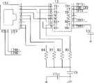
如图7所示,监测数据中转远程传输接口模块5-2-3包括第三电平转换芯片U2,第十一倍压电解电容C15、第十二倍压电解电容C16、第十三倍压电解电容C17、第十四倍压电解电容C18、第十五倍压电解电容C19;第十一倍压电解电容C15正极与第三电平转换芯片U2的1脚连接,负极与第三电平转换芯片U2的3脚连接,第十二倍压电解电容C16正极与第三电平转换芯片U2的4脚连接,负极与第三电平转换芯片U2的5脚连接,第十三倍压电解电容C17负极、第十四倍压电解电容C18正极和第三电平转换芯片U2的16脚与5V电源连接;第十三倍压电解电容C17正极与第三电平转换芯片U2的2脚连接,第十四倍压电解电容C18负极接地,第十五倍压电解电容C19负极与第三电平转换芯片U2的6脚连接,正极接地;As shown in Figure 7, the monitoring data transfer remote transmission interface module 5-2-3 includes a third level conversion chip U2, an eleventh double voltage electrolytic capacitor C15, a twelfth double voltage electrolytic capacitor C16, a thirteenth double voltage electrolytic capacitor The doubler voltage electrolytic capacitor C17, the fourteenth doubler voltage electrolytic capacitor C18, and the fifteenth doubler voltage electrolytic capacitor C19; the positive electrode of the eleventh doubler voltage electrolytic capacitor C15 is connected to pin 1 of the third level conversion chip U2, The negative pole is connected to pin 3 of the third level conversion chip U2, the positive pole of the twelfth multiplier electrolytic capacitor C16 is connected to pin 4 of the third level conversion chip U2, and the negative pole is connected to pin 5 of the third level conversion chip U2 , the negative pole of the thirteenth double voltage electrolytic capacitor C17, the positive pole of the fourteenth double voltage electrolytic capacitor C18 and the 16 pin of the third level conversion chip U2 are connected to the 5V power supply; the positive pole of the thirteenth double voltage electrolytic capacitor C17 is connected to the first The pin 2 of the three-level conversion chip U2 is connected, the negative pole of the fourteenth multiplier voltage electrolytic capacitor C18 is grounded, the negative pole of the fifteenth multiplier voltage electrolytic capacitor C19 is connected to the pin 6 of the third level conversion chip U2, and the positive pole is grounded;
五个倍压电解电容个容量值均为0.1uF,U2的11脚、12脚分别接核心板总线5-3中EM9160_CN1的14脚、13脚,U2的13、14脚分别接标准RS232DB9连接器JP2的3、2脚,U2的15、16脚分别接信号地和5V电源;JP2的5脚接信号地,JP2的1脚、4脚、6脚、7脚、8脚和9脚分别接核心板总线5-3中EM9160_CN1的20脚、18脚、17脚、16脚、15脚和19脚。The capacity values of the five voltage doubler electrolytic capacitors are all 0.1uF.
监测数据中转远程传输接口模块5-2-3提供一个标准9线RS232串口。当底板5-1用于水下数据采集与存储模块12时,可借助该9线RS232串口将数据发送至耦合信号发送模块11;当底板5-1用于浮标数据转发模块5时,该9线RS232串口用于将剖面监测数据发送至浮标数据转发模块5,再由浮标数据转发模块5进行剖面监测数据的远程转发。Monitoring data transfer remote transmission interface module 5-2-3 provides a standard 9-wire RS232 serial port. When the base plate 5-1 is used for the underwater data acquisition and
如图8所示,控制量接口模块5-2-4包括状态指示灯供电调压器U5、第五高频滤波电容C3、第三低频滤波电解电容C4、第一IO状态指示灯DS2、第二IO状态指示灯DS3、第三IO状态指示灯DS4、第四IO状态指示灯DS5、第五IO状态指示灯DS6、第六IO状态指示灯DS7、第七IO状态指示灯DS8、第八IO状态指示灯DS8、第九IO状态指示灯DS10、第一限流电阻R7、第二限流电阻R8、第三限流电阻R9、第四限流电阻R10、第五限流电阻R11、第六限流电阻R12、第七限流电阻R13、第八限流电阻R14、第九限流电阻R15;第五高频滤波电容C3一端、第三低频滤波电解电容C4正极与状态指示灯供电调压器U5的输出端连接;第五高频滤波电容C3另一端、第三低频滤波电解电容C4负极、状态指示灯供电调压器U5的接地端接接地;状态指示灯供电调压器U5的输入端接5V电源;As shown in Figure 8, the control quantity interface module 5-2-4 includes a status indicator power supply voltage regulator U5, a fifth high-frequency filter capacitor C3, a third low-frequency filter electrolytic capacitor C4, a first IO status indicator DS2, a second The second IO status indicator DS3, the third IO status indicator DS4, the fourth IO status indicator DS5, the fifth IO status indicator DS6, the sixth IO status indicator DS7, the seventh IO status indicator DS8, the eighth IO Status indicator DS8, ninth IO status indicator DS10, first current limiting resistor R7, second current limiting resistor R8, third current limiting resistor R9, fourth current limiting resistor R10, fifth current limiting resistor R11, sixth Current-limiting resistor R12, seventh current-limiting resistor R13, eighth current-limiting resistor R14, ninth current-limiting resistor R15; one end of the fifth high-frequency filter capacitor C3, the positive pole of the third low-frequency filter electrolytic capacitor C4 and the status indicator power supply voltage regulation The output end of the device U5 is connected; the other end of the fifth high-frequency filter capacitor C3, the negative pole of the third low-frequency filter electrolytic capacitor C4, and the ground terminal of the status indicator power supply voltage regulator U5 are grounded; the input of the status indicator power supply voltage regulator U5 Terminate the 5V power supply;
第一限流电阻R7一端、第二限流电阻R8一端、第三限流电阻R9一端、第四限流电阻R10一端、第五限流电阻R11一端、第六限流电阻R12一端、第七限流电阻R13一端、第八限流电阻R14一端、第九限流电阻R15一端并联后接状态指示灯供电调压器U5的输出端;第一限流电阻R7另一端接第一IO状态指示灯DS2的正极,第二限流电阻R8另一端接第二IO状态指示灯DS3的正极,第三限流电阻R9另一端接第三IO状态指示灯DS4的正极,第四限流电阻R10另一端接第四IO状态指示灯DS5的正极,第五限流电阻R11另一端接第五IO状态指示灯DS6的正极,第六限流电阻R12另一端接第六IO状态指示灯DS7的正极,第七限流电阻R13另一端接第七IO状态指示灯DS8的正极,第八限流电阻R14另一端接第八IO状态指示灯DS9的正极,第九限流电阻R15另一端接第九IO状态指示灯DS10的正极;One end of the first current-limiting resistor R7, one end of the second current-limiting resistor R8, one end of the third current-limiting resistor R9, one end of the fourth current-limiting resistor R10, one end of the fifth current-limiting resistor R11, one end of the sixth current-limiting resistor R12, one end of the seventh One end of the current-limiting resistor R13, one end of the eighth current-limiting resistor R14, and one end of the ninth current-limiting resistor R15 are connected in parallel to the output end of the status indicator power supply voltage regulator U5; the other end of the first current-limiting resistor R7 is connected to the first IO status indicator The positive pole of the lamp DS2, the other end of the second current-limiting resistor R8 is connected to the positive pole of the second IO status indicator DS3, the other end of the third current-limiting resistor R9 is connected to the positive pole of the third IO status indicator DS4, and the other end of the fourth current-limiting resistor R10 One end is connected to the positive pole of the fourth IO status indicator DS5, the other end of the fifth current limiting resistor R11 is connected to the positive pole of the fifth IO status indicator DS6, the other end of the sixth current limiting resistor R12 is connected to the positive pole of the sixth IO status indicator DS7, The other end of the seventh current limiting resistor R13 is connected to the positive pole of the seventh IO status indicator DS8, the other end of the eighth current limiting resistor R14 is connected to the positive pole of the eighth IO status indicator DS9, and the other end of the ninth current limiting resistor R15 is connected to the ninth IO The positive pole of the status indicator DS10;
第五高频滤波电容C3容量值为0.1uF的、第三低频滤波电解电容C4容量值为10uF,控制量接口模块5-2-4可提供9个GPIO用于接收或输出数字开关信号,9个状态指示灯用于显示对应的GPIO口开关状态,便于调试。当底板5-1用于水下数据采集与存储模块12时,可借助这些GPIO实现对单向锁定开关10或其他相关水下设备的控制。The fifth high-frequency filter capacitor C3 has a capacity value of 0.1uF, the third low-frequency filter electrolytic capacitor C4 has a capacity value of 10uF, and the control quantity interface module 5-2-4 can provide 9 GPIOs for receiving or outputting digital switching signals, 9 A status indicator is used to display the switch status of the corresponding GPIO port, which is convenient for debugging. When the bottom board 5-1 is used for the underwater data acquisition and
如图9所示,调试接口模块5-2-5包括网络隔离变压器U1、RJ45网络接头CN1、第一匹配电阻R1、第二匹配电阻R2、第三匹配电阻R3、第四匹配电阻R4、第六高频滤波电容C5、耐压电容C6和隔离电容C7;As shown in Figure 9, the debugging interface module 5-2-5 includes a network isolation transformer U1, an RJ45 network connector CN1, a first matching resistor R1, a second matching resistor R2, a third matching resistor R3, a fourth matching resistor R4, a Six high-frequency filter capacitors C5, withstand voltage capacitors C6 and isolation capacitors C7;
第一匹配电阻R1的一端、第二匹配电阻R2的一端、第三匹配电阻R3的一端和第四匹配电阻R4的一端与耐压电容C6一端连接,耐压电容C6另一端与隔离电容C7一端连接,隔离电容C7另一端接地,第一匹配电阻R1的另一端与网络隔离变压器U1的10脚连接,第二匹配电阻R2的另一端与网络隔离变压器U1的15脚连接,第三匹配电阻R3的另一端与RJ45网络接头CN1的4脚和5脚连接,第四匹配电阻R4的另一端与RJ45网络接头CN1的7脚和8脚连接,网络隔离变压器U1的16脚与RJ45网络接头CN1的1脚连接,网络隔离变压器U1的14脚与RJ45网络接头CN1的脚连接,网络隔离变压器U1的11脚与RJ45网络接头CN1的3脚连接,网络隔离变压器U1的9脚与RJ45网络接头CN1的6脚连接,高频滤波电容C5的一端接网络隔离变压器U1的7脚,另一端接地;One end of the first matching resistor R1, one end of the second matching resistor R2, one end of the third matching resistor R3 and one end of the fourth matching resistor R4 are connected to one end of the withstand voltage capacitor C6, and the other end of the withstand voltage capacitor C6 is connected to one end of the isolation capacitor C7 connection, the other end of the isolation capacitor C7 is grounded, the other end of the first matching resistor R1 is connected to the 10-pin of the network isolation transformer U1, the other end of the second matching resistor R2 is connected to the 15-pin of the network isolation transformer U1, and the third matching resistor R3 The other end of the RJ45 network connector CN1 is connected to pin 4 and pin 5, the other end of the fourth matching resistor R4 is connected to pin 7 and pin 8 of the RJ45 network connector CN1, and pin 16 of the network isolation transformer U1 is connected to the RJ45 network connector CN1. 1-pin connection, the 14-pin of the network isolation transformer U1 is connected with the pin of the RJ45 network connector CN1, the 11-pin of the network isolation transformer U1 is connected with the 3-pin of the RJ45 network connector CN1, the 9-pin of the network isolation transformer U1 is connected with the RJ45 network connector CN1 6-pin connection, one end of the high-frequency filter capacitor C5 is connected to the 7-pin of the network isolation transformer U1, and the other end is grounded;
第六高频滤波电容C5容量值为0.1uF,耐压电容C6参数为10nF/2kV,隔离电容C7容量值为0.1uF,U1的1脚、2脚、3脚、6脚和8脚分别接于核心板总线5-3中EM9160_CN1的1脚、9脚、2脚、3脚和4脚,U1的9脚、11脚、14脚、16脚分别接于CN1的6脚、3脚、2脚、1脚;CN1的11脚、12脚分别接于核心板总线5-3中EM9160_CN1的5、6脚;The capacity value of the sixth high-frequency filter capacitor C5 is 0.1uF, the parameter of the withstand voltage capacitor C6 is 10nF/2kV, the capacity value of the isolation capacitor C7 is 0.1uF, and pins 1, 2, 3, 6 and 8 of U1 are respectively connected to Pin 1,
调试接口模块5-2-5提供网络调试接口,用于程序调试。The debugging interface module 5-2-5 provides a network debugging interface for program debugging.
如图10所示,耦合信号发送模块11由数据接口11-1、调制电路11-2、功放电路11-3构成。数据接口11-1通过串口与水下数据采集与存储模块12,调制电路11-2一端与数据接口11-1信号连接,另一端与功放电路11-3一端信号连接,功放电路11-3一端与调制电路11-2信号连接,另一端与耦合信号发送线圈8连接。其中,数据接口11-1采用RS232串口,用于连接水下数据采集与存储模块12,以便接收待发送的剖面监测数据;调制电路11-2用于将待发送数据信号采用幅度键控(ASK)方式调制到一定频率的载波信号上;功放电路采用甲乙类互补推挽功率放大电路,用于将经过调制的待发送数据信号进行功率放大。As shown in FIG. 10, the coupling
如图11所示,耦合信号接收模块6由放大电路6-1、前端滤波电路6-2、检波电路6-3、后端滤波电路6-4、数字信号还原电路6-5和数据接口6-6构成。其中,放大电路6-1一端连接耦合信号接收线圈7,另一端与前端滤波电路6-2一端信号连接,前端滤波电路6-2另一端与检波电路6-3一端信号连接,检波电路6-3另一端与后端滤波电路6-4一端信号连接,后端滤波电路6-4与数字信号还原电路6-5一端信号连接,数字信号还原电路6-5另一端连接数据接口6-6。As shown in Figure 11, the coupled
其中,放大电路6-1采用集成运放构成的电压放大电路实现接收线圈7上微弱电压信号的放大;前端滤波电路采用集成运放构成的有源低通滤波器滤除传输过程中产生的高频噪声信号;检波电路用于获取已发生畸变的基带信号;后端滤波电路采用集成运放构成的有源低通滤波器,用于进一步滤除高频干扰信号;数字信号还原电路6-5用于将后端滤波电路6-4产生的模拟信号还原为数字信号;数据接口采用RS232串口将还原的数字信号传输至数据接收终端。Among them, the amplifying circuit 6-1 adopts a voltage amplifying circuit composed of an integrated operational amplifier to amplify the weak voltage signal on the receiving
如图12所示,发送线圈8和接收线圈7的参数和绕制方法一致,均采用Φ1.2mm漆包线绕制,线圈形状为圆形,直径7.5cm,匝数为10。绕制好的线圈具有两个端子,若将线圈作为发送线圈8,则其中一个端子连接功放电路11-3的输出端,另一端连接耦合信号发送模块11的接地端;若将线圈作为接收线圈7,则其中一个端子连接放大电路6-1的输出端,另一端连接耦合信号接收模块6的接地端。As shown in Figure 12, the parameters and winding methods of the sending
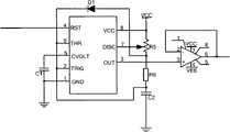
如图13所示,所述的调制电路11-2包括时基电路LM555,第一充放电电容C1、第二充放电电容C2,可调电阻R5、频率设置电阻R6、充放电引导二极管D1和运算放大器;第一充放电电容C1的一端和时基电路LM555的1脚接地,第一充放电电容C1的另一端与时基电路LM555的5脚连接,充放电引导二极管D1的阴极、时基电路LM555的6脚、时基电路LM555的2脚、频率设置电阻R6的一端与第二充放电电容C2的一端连接,第二充放电电容C2的另一端接地,频率设置电阻R6的另一端、充放电引导二极管D1的阳极和时基电路LM555的7脚与可调电阻R5一端连接,可调电阻R5另一端和时基电路LM555的8脚接5V电源,可调电阻R5的可调端与时基电路LM555的7脚连接;时基电路LM555的3脚与运算放大器的同相输入端连接,运算放大器的反相输入端与运算放大器的输出端连接。As shown in Figure 13, the modulation circuit 11-2 includes a time base circuit LM555, a first charging and discharging capacitor C1, a second charging and discharging capacitor C2, an adjustable resistor R5, a frequency setting resistor R6, a charging and discharging guiding diode D1 and Operational amplifier; one end of the first charging and discharging capacitor C1 is grounded to pin 1 of the time base circuit LM555, the other end of the first charging and discharging capacitor C1 is connected to pin 5 of the time base circuit LM555, the cathode of the charging and discharging guiding diode D1, the time base Pin 6 of the circuit LM555, pin 2 of the time base circuit LM555, one end of the frequency setting resistor R6 is connected to one end of the second charging and discharging capacitor C2, the other end of the second charging and discharging capacitor C2 is grounded, the other end of the frequency setting resistor R6, The anode of the charging and discharging guiding diode D1 is connected to the 7 pin of the time base circuit LM555 and one end of the adjustable resistor R5, the other end of the adjustable resistor R5 and the 8 pin of the time base circuit LM555 are connected to the 5V power supply, the adjustable end of the adjustable resistor R5 is connected to The 7 pins of the time base circuit LM555 are connected; the 3 pins of the time base circuit LM555 are connected with the non-inverting input terminal of the operational amplifier, and the inverting input terminal of the operational amplifier is connected with the output terminal of the operational amplifier.
调制电路5-2的作用就是将待发送数据进行ASK载波调制,LM555通过R5、R6、C2产生一定频率的方波信号,R5选用10KΩ的可变电阻,R6选用3KΩ电阻,C2选用0.001uF电容,通过调节R5的阻值就可产生频率为200KHz的载波,C1选用0.1uF电容,D1选用普通二极管,通过待发送数据在复位端的变化,就可以对信号进行ASK调制,并最终通过LM555的3引脚将调制后的信号输出,LM318N用做电压跟随器,增大输出信号的带负载能力。The role of modulation circuit 5-2 is to modulate the data to be sent by ASK carrier. LM555 generates a square wave signal of a certain frequency through R5, R6, and C2. R5 uses a 10KΩ variable resistor, R6 uses a 3KΩ resistor, and C2 uses a 0.001uF capacitor , by adjusting the resistance of R5, a carrier wave with a frequency of 200KHz can be generated, C1 uses a 0.1uF capacitor, D1 uses an ordinary diode, and through the change of the data to be sent at the reset end, the signal can be ASK modulated, and finally through the
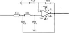
如图14所示,所述的前端滤波电路6-2包括第一截止频率设置电容C6、第二截止频率设置电容C7,第一截止频率设置电阻R10、第二截止频率设置电阻R11、第一负反馈电阻R12、第二负反馈电阻R13和运算放大器OP07CN;As shown in Figure 14, the front-end filter circuit 6-2 includes a first cut-off frequency setting capacitor C6, a second cut-off frequency setting capacitor C7, a first cut-off frequency setting resistor R10, a second cut-off frequency setting resistor R11, a first Negative feedback resistor R12, the second negative feedback resistor R13 and operational amplifier OP07CN;
第二截止频率设置电阻R11一端、第一截止频率设置电容C6一端与第一截止频率设置电阻R10的一端连接,第二截止频率设置电阻R11另一端、第二截止频率设置电容C7一端与运算放大器OP07CN的同相输入端连接,第二截止频率设置电容C7另一端接地,第一截止频率设置电容C6另一端、第二负反馈电阻R13一端与运算放大器OP07CN的输出端连接,第二负反馈电阻R13另一端、第一负反馈电阻R12一端与运算放大器OP07CN的反相输入端连接,第一负反馈电阻R12另一端接地;One end of the second cutoff frequency setting resistor R11 and one end of the first cutoff frequency setting capacitor C6 are connected to one end of the first cutoff frequency setting resistor R10, the other end of the second cutoff frequency setting resistor R11 and one end of the second cutoff frequency setting capacitor C7 are connected to the operational amplifier The non-inverting input terminal of OP07CN is connected, the other end of the second cutoff frequency setting capacitor C7 is grounded, the other end of the first cutoff frequency setting capacitor C6, and one end of the second negative feedback resistor R13 are connected to the output terminal of the operational amplifier OP07CN, and the second negative feedback resistor R13 The other end, one end of the first negative feedback resistor R12 is connected to the inverting input end of the operational amplifier OP07CN, and the other end of the first negative feedback resistor R12 is grounded;
前端滤波电路6-2的作用为滤除信号传输过程中产生的高频噪声信号,C6、C7选择0.001uF电容,R10、R11选用680Ω电阻,R12选用10KΩ电阻,R13选用4.7KΩ电阻,与运算放大器OP07CN一起构成有源低通滤波器,滤除载波频率200KHz以外的高频噪声信号。经滤波后的信号输出至检波电路6-3。The function of the front-end filter circuit 6-2 is to filter out the high-frequency noise signal generated during the signal transmission process. C6 and C7 select 0.001uF capacitors, R10 and R11 select 680Ω resistors, R12 selects 10KΩ resistors, and R13 selects 4.7KΩ resistors. Amplifier OP07CN constitutes an active low-pass filter together to filter out high-frequency noise signals other than the carrier frequency of 200KHz. The filtered signal is output to the detection circuit 6-3.
如图15所示,所述的检波电路6-3包括整流二极管D4,第三充放电电容C8,充放电电阻R14,运算放大器LF351AN。整流二极管D4一端、第三充放电电容C8一端、充放电电阻R14一端与运算放大器LF351AN的同相输入端连接,第三充放电电容C8另一端和充放电电阻R14另一端接地,运算放大器LF351AN的反相输入端与运算放大器LF351AN的输出端连接。As shown in FIG. 15 , the detection circuit 6-3 includes a rectifier diode D4, a third charge and discharge capacitor C8, a charge and discharge resistor R14, and an operational amplifier LF351AN. One end of the rectifier diode D4, one end of the third charge and discharge capacitor C8, and one end of the charge and discharge resistor R14 are connected to the non-inverting input end of the operational amplifier LF351AN, the other end of the third charge and discharge capacitor C8 and the other end of the charge and discharge resistor R14 are grounded, and the opposite end of the operational amplifier LF351AN The phase input terminal is connected with the output terminal of the operational amplifier LF351AN.
检波电路6-3的作用是将调制在载波信号上的有用耦合信号解调出来,D4选用肖特基二极管,C8选用0.01uF电容,R14选用1.5KΩ电阻,D4、C8、R14构成标准的二极管整流检波电路,将波特率为9600bps的有用信号解调出来。LF351AN用作电压跟随器,增大输出信号的带负载能力。包络检波后的信号输出至后端滤波电路6-4。The function of the detection circuit 6-3 is to demodulate the useful coupling signal modulated on the carrier signal. D4 uses a Schottky diode, C8 uses a 0.01uF capacitor, and R14 uses a 1.5KΩ resistor. D4, C8, and R14 form a standard diode The rectification and detection circuit demodulates the useful signal with a baud rate of 9600bps. LF351AN is used as a voltage follower to increase the load capacity of the output signal. The signal after envelope detection is output to the back-end filter circuit 6-4.
如图16所示,所述的数字信号还原电路6-5包括滤波电容C12、第一偏置电阻R22、第二偏置电阻R23、第一上限电压分压电阻R19、第二上限电压分压电阻R20、第一下限电压分压电阻R24、第二下限电压分压电阻R25、第一上拉电阻R21、第二上拉电阻R26、电压比较器LM339AN和集成与非门SN74LS00N;As shown in Figure 16, the digital signal restoration circuit 6-5 includes a filter capacitor C12, a first bias resistor R22, a second bias resistor R23, a first upper limit voltage divider resistor R19, a second upper limit voltage divider Resistor R20, first lower limit voltage divider resistor R24, second lower limit voltage divider resistor R25, first pull-up resistor R21, second pull-up resistor R26, voltage comparator LM339AN and integrated NAND gate SN74LS00N;
第一偏置电阻R22一端、第二偏置电阻R23一端、电压比较器LM339AN的5脚和电压比较器LM339AN的7脚与滤波电容C12的一端,电压比较器LM339AN的4脚、第一上限电压分压电阻R19的一端与第二上限电压分压电阻R20的一端连接,第二上限电压分压电阻R20的另一端、电压比较器LM339AN的3脚和第一上拉电阻R21一端接+5V,电压比较器LM339AN的2脚、第一上拉电阻R21另一端、集成与非门SN74LS00N的2脚与集成与非门SN74LS00N的1脚连接,第一上限电压分压电阻R19的另一端接地;One end of the first bias resistor R22, one end of the second bias resistor R23,
电压比较器LM339AN的6脚、第一下限电压分压电阻R24的一端与第二下限电压分压电阻R25的一端连接,第二下限电压分压电阻R25的另一端、电压比较器LM339AN的3脚和第二上拉电阻R26一端接+5V,第二上拉电阻R26另一端与电压比较器LM339AN的1脚连接,第一下限电压分压电阻R24的另一端接地;
数字信号还原电路6-5的作用是将后端滤波电路6-4输出的模拟信号转换为数字信号。电容C12选用10uF电容,用于使后端滤波电路6-4输出的信号更加平滑;电阻R19、R24选用1KΩ电阻,R20、R25选用10KΩ可变电阻,R21、R22、R23、R26选用10KΩ电阻,与LM339AN构成阈值比较电路,并与SN74LS00N构成施密特触发电路,将9600bps的数字信号还原出来,还原后的信号即为水下数据采集与存储模块12发出的剖面监测数据。The function of the digital signal restoration circuit 6-5 is to convert the analog signal output by the back-end filter circuit 6-4 into a digital signal. Capacitor C12 is a 10uF capacitor, which is used to make the signal output by the back-end filter circuit 6-4 smoother; resistors R19 and R24 are 1KΩ resistors, R20 and R25 are 10KΩ variable resistors, and R21, R22, R23, and R26 are 10KΩ resistors. It forms a threshold comparison circuit with LM339AN and a Schmitt trigger circuit with SN74LS00N to restore the 9600bps digital signal, and the restored signal is the profile monitoring data sent by the underwater data acquisition and
本发明的工作过程为:剖面仪在下降或升浮过程中其内部搭载的传感器通过传感器数据接口将剖面监测数据传输至水下数据采集与存储模块进行自容存储;当剖面仪上浮至浮标体底部一定距离范围内,耦合信号收发模块可以建立稳定的通讯连接时,水下数据采集与存储模块发送指令关闭单向锁定装置,剖面仪停止上浮,水下数据采集与存储模块将存储在SD卡或U盘中的剖面监测数据通过耦合信号发送和接收模块耦合传输至浮标数据转发模块;浮标数据转发模块获得剖面监测数据后,将其存储在自身的SD卡或U盘中,然后开启数传电台或者通讯卫星的通信功能,完成剖面监测数据的远程转发;之后,水下数据采集与存储模块发送指令打开单向锁定装置,剖面仪将再次下降,开始新的数据采集周期。The working process of the present invention is as follows: when the profiler is descending or ascending, the internal sensor transmits the profile monitoring data to the underwater data acquisition and storage module through the sensor data interface for self-contained storage; when the profiler floats to the buoy body Within a certain distance from the bottom, when the coupling signal transceiver module can establish a stable communication connection, the underwater data acquisition and storage module sends an instruction to close the one-way locking device, the profiler stops floating, and the underwater data acquisition and storage module will be stored in the SD card Or the profile monitoring data in the U disk is coupled and transmitted to the buoy data forwarding module through the coupling signal sending and receiving module; after the buoy data forwarding module obtains the profile monitoring data, it stores it in its own SD card or U disk, and then starts the data transmission The communication function of the radio station or communication satellite completes the remote forwarding of the profile monitoring data; after that, the underwater data acquisition and storage module sends an instruction to open the one-way locking device, and the profiler will descend again to start a new data acquisition cycle.
Claims (1)
Priority Applications (1)
| Application Number | Priority Date | Filing Date | Title |
|---|---|---|---|
| CN2009101541225ACN101738179B (en) | 2009-11-05 | 2009-11-05 | Inductive coupling-based anchoring self-lifting profile monitoring buoy |
Applications Claiming Priority (1)
| Application Number | Priority Date | Filing Date | Title |
|---|---|---|---|
| CN2009101541225ACN101738179B (en) | 2009-11-05 | 2009-11-05 | Inductive coupling-based anchoring self-lifting profile monitoring buoy |
Publications (2)
| Publication Number | Publication Date |
|---|---|
| CN101738179Atrue CN101738179A (en) | 2010-06-16 |
| CN101738179B CN101738179B (en) | 2011-08-31 |
Family
ID=42461957
Family Applications (1)
| Application Number | Title | Priority Date | Filing Date |
|---|---|---|---|
| CN2009101541225AExpired - Fee RelatedCN101738179B (en) | 2009-11-05 | 2009-11-05 | Inductive coupling-based anchoring self-lifting profile monitoring buoy |
Country Status (1)
| Country | Link |
|---|---|
| CN (1) | CN101738179B (en) |
Cited By (26)
| Publication number | Priority date | Publication date | Assignee | Title |
|---|---|---|---|---|
| CN102167136A (en)* | 2010-12-16 | 2011-08-31 | 中国船舶重工集团公司第七一○研究所 | Ocean lifting submerged buoy system |
| CN103112551A (en)* | 2013-01-24 | 2013-05-22 | 浙江海洋学院 | Wind wave resistant ocean profile monitoring buoy |
| CN103267518A (en)* | 2013-05-07 | 2013-08-28 | 浙江大学 | Artificial upwelling marine environment multi-parameter real-time continuous three-dimensional monitoring system |
| CN103770911A (en)* | 2014-01-27 | 2014-05-07 | 国家海洋局第一海洋研究所 | Deep-sea observing buoy system based on inductive coupling and satellite communication techniques |
| CN104443280A (en)* | 2013-09-24 | 2015-03-25 | 国家海洋局第二海洋研究所 | Ocean buoy |
| CN104802936A (en)* | 2015-04-28 | 2015-07-29 | 中国农业大学 | Paralic environment monitoring buoy and system |
| CN104931395A (en)* | 2015-05-12 | 2015-09-23 | 杭州电子科技大学 | Submarine plankton particle-size spectra laser detection circuit |
| CN105235826A (en)* | 2015-10-22 | 2016-01-13 | 黑龙江省博凯科技开发有限公司 | Multifunctional marine environment monitoring platform |
| CN105548516A (en)* | 2015-12-30 | 2016-05-04 | 浙江大学 | Continuous in-situ monitoring platform device in hypoxia sea area |
| CN103727983B (en)* | 2014-01-08 | 2016-07-06 | 苏州热工研究院有限公司 | A kind of wireless hydrologic monitoring device of nuclear power plant |
| CN105842412A (en)* | 2016-03-24 | 2016-08-10 | 中国科学院重庆绿色智能技术研究院 | Water environment vertical distribution comprehensive on-line monitoring buoy and monitoring system |
| CN106080978A (en)* | 2016-06-07 | 2016-11-09 | 熊学军 | Full packing formula sea drifting buoy ball float |
| CN106643672A (en)* | 2016-12-16 | 2017-05-10 | 哈尔滨工程大学 | Real-time transmission ocean power parameter buoy system |
| CN107323191A (en)* | 2017-04-14 | 2017-11-07 | 赵焕新 | Pleasantly surprised water-bed row electric automobile |
| CN107991679A (en)* | 2017-11-27 | 2018-05-04 | 天津科技大学 | A kind of monitoring method and monitoring device of planktonic organism vertical migration |
| CN107990880A (en)* | 2017-11-30 | 2018-05-04 | 上海海洋大学 | Marine ecology monitering buoy device |
| CN108116642A (en)* | 2018-01-17 | 2018-06-05 | 国家海洋局第二海洋研究所 | A kind of semi-submersible offshore profiling observation intelligent robot |
| CN109302697A (en)* | 2018-07-31 | 2019-02-01 | 大连理工大学 | A device and method for underwater data wireless return based on buoy and SD card temporary storage |
| CN112304268A (en)* | 2019-07-29 | 2021-02-02 | 意富资产有限公司 | Equipment and method for profiling pile hole |
| CN112423258A (en)* | 2020-12-04 | 2021-02-26 | 中国船舶重工集团有限公司第七一0研究所 | Satellite alarm device with double-head antenna |
| CN112556792A (en)* | 2020-12-24 | 2021-03-26 | 邱爱平 | Method for automatically monitoring sedimentation state of river bottom sludge |
| CN113501091A (en)* | 2021-04-22 | 2021-10-15 | 浙江大学 | Ice-based profiler release device and data acquisition system |
| CN113525614A (en)* | 2021-08-13 | 2021-10-22 | 山东大学 | Ocean profile carbon dioxide concentration observation device and working method thereof |
| CN113920695A (en)* | 2021-10-26 | 2022-01-11 | 杭州电子科技大学 | Emergency alarm system for underwater autonomous robot |
| CN114440820A (en)* | 2022-01-12 | 2022-05-06 | 中国地质大学(武汉) | Landslide underwater deformation characteristic transfer monitoring equipment and method |
| CN118323340A (en)* | 2024-06-11 | 2024-07-12 | 东海实验室 | Low-energy-consumption floating sea gas automatic observation platform |
Families Citing this family (1)
| Publication number | Priority date | Publication date | Assignee | Title |
|---|---|---|---|---|
| TW201412603A (en)* | 2012-09-21 | 2014-04-01 | Nat Applied Res Laboratories | Floating type monitoring device |
- 2009
- 2009-11-05CNCN2009101541225Apatent/CN101738179B/ennot_activeExpired - Fee Related
Cited By (34)
| Publication number | Priority date | Publication date | Assignee | Title |
|---|---|---|---|---|
| CN102167136B (en)* | 2010-12-16 | 2013-06-05 | 中国船舶重工集团公司第七一○研究所 | Ocean lifting submerged buoy system |
| CN102167136A (en)* | 2010-12-16 | 2011-08-31 | 中国船舶重工集团公司第七一○研究所 | Ocean lifting submerged buoy system |
| CN103112551B (en)* | 2013-01-24 | 2015-10-21 | 浙江海洋学院 | Wind-proof and wave-proof ocean profile monitering buoy |
| CN103112551A (en)* | 2013-01-24 | 2013-05-22 | 浙江海洋学院 | Wind wave resistant ocean profile monitoring buoy |
| CN103267518A (en)* | 2013-05-07 | 2013-08-28 | 浙江大学 | Artificial upwelling marine environment multi-parameter real-time continuous three-dimensional monitoring system |
| CN104443280B (en)* | 2013-09-24 | 2016-11-02 | 国家海洋局第二海洋研究所 | an ocean buoy |
| CN104443280A (en)* | 2013-09-24 | 2015-03-25 | 国家海洋局第二海洋研究所 | Ocean buoy |
| CN103727983B (en)* | 2014-01-08 | 2016-07-06 | 苏州热工研究院有限公司 | A kind of wireless hydrologic monitoring device of nuclear power plant |
| CN103770911B (en)* | 2014-01-27 | 2016-05-25 | 国家海洋局第一海洋研究所 | A kind of deep-sea observation buoyage based on induction coupling and communication technology of satellite |
| CN103770911A (en)* | 2014-01-27 | 2014-05-07 | 国家海洋局第一海洋研究所 | Deep-sea observing buoy system based on inductive coupling and satellite communication techniques |
| CN104802936A (en)* | 2015-04-28 | 2015-07-29 | 中国农业大学 | Paralic environment monitoring buoy and system |
| CN104931395A (en)* | 2015-05-12 | 2015-09-23 | 杭州电子科技大学 | Submarine plankton particle-size spectra laser detection circuit |
| CN105235826A (en)* | 2015-10-22 | 2016-01-13 | 黑龙江省博凯科技开发有限公司 | Multifunctional marine environment monitoring platform |
| CN105548516A (en)* | 2015-12-30 | 2016-05-04 | 浙江大学 | Continuous in-situ monitoring platform device in hypoxia sea area |
| CN105842412A (en)* | 2016-03-24 | 2016-08-10 | 中国科学院重庆绿色智能技术研究院 | Water environment vertical distribution comprehensive on-line monitoring buoy and monitoring system |
| CN106080978A (en)* | 2016-06-07 | 2016-11-09 | 熊学军 | Full packing formula sea drifting buoy ball float |
| CN106643672A (en)* | 2016-12-16 | 2017-05-10 | 哈尔滨工程大学 | Real-time transmission ocean power parameter buoy system |
| CN107323191A (en)* | 2017-04-14 | 2017-11-07 | 赵焕新 | Pleasantly surprised water-bed row electric automobile |
| CN107991679A (en)* | 2017-11-27 | 2018-05-04 | 天津科技大学 | A kind of monitoring method and monitoring device of planktonic organism vertical migration |
| CN107990880A (en)* | 2017-11-30 | 2018-05-04 | 上海海洋大学 | Marine ecology monitering buoy device |
| CN107990880B (en)* | 2017-11-30 | 2021-05-25 | 上海海洋大学 | Marine ecological monitoring buoy device |
| CN108116642A (en)* | 2018-01-17 | 2018-06-05 | 国家海洋局第二海洋研究所 | A kind of semi-submersible offshore profiling observation intelligent robot |
| CN109302697B (en)* | 2018-07-31 | 2021-05-18 | 大连理工大学 | Underwater data wireless return device and method based on temporary storage of buoy and SD card |
| CN109302697A (en)* | 2018-07-31 | 2019-02-01 | 大连理工大学 | A device and method for underwater data wireless return based on buoy and SD card temporary storage |
| CN112304268A (en)* | 2019-07-29 | 2021-02-02 | 意富资产有限公司 | Equipment and method for profiling pile hole |
| CN112423258A (en)* | 2020-12-04 | 2021-02-26 | 中国船舶重工集团有限公司第七一0研究所 | Satellite alarm device with double-head antenna |
| CN112556792A (en)* | 2020-12-24 | 2021-03-26 | 邱爱平 | Method for automatically monitoring sedimentation state of river bottom sludge |
| CN113501091A (en)* | 2021-04-22 | 2021-10-15 | 浙江大学 | Ice-based profiler release device and data acquisition system |
| CN113525614A (en)* | 2021-08-13 | 2021-10-22 | 山东大学 | Ocean profile carbon dioxide concentration observation device and working method thereof |
| CN113920695A (en)* | 2021-10-26 | 2022-01-11 | 杭州电子科技大学 | Emergency alarm system for underwater autonomous robot |
| CN114440820A (en)* | 2022-01-12 | 2022-05-06 | 中国地质大学(武汉) | Landslide underwater deformation characteristic transfer monitoring equipment and method |
| CN118323340A (en)* | 2024-06-11 | 2024-07-12 | 东海实验室 | Low-energy-consumption floating sea gas automatic observation platform |
| CN118323340B (en)* | 2024-06-11 | 2024-09-24 | 东海实验室 | Low-energy-consumption floating sea gas automatic observation platform |
| US12276499B2 (en) | 2024-06-11 | 2025-04-15 | Donghai Laboratory | Low-energy-consumption floating automatic oceanographic and meteorological observation platform |
Also Published As
| Publication number | Publication date |
|---|---|
| CN101738179B (en) | 2011-08-31 |
Similar Documents
| Publication | Publication Date | Title |
|---|---|---|
| CN101738179A (en) | Inductive coupling-based anchoring self-lifting profile monitoring buoy | |
| CN201523387U (en) | An anchored self-elevating profile monitoring buoy | |
| CN108540578A (en) | Communication control system with subsurface communication network Yu Beidou satellite communication function | |
| CN103970295A (en) | Mouse with power supplied by wireless power supply | |
| CN112271830A (en) | Ocean buoy system for realizing parallel transmission of electric energy and data based on frequency division multiplexing | |
| CN102034345B (en) | Twisted pair carrier communication circuit for automatic meter reading system and method thereof | |
| CN114865761A (en) | A passive wireless image acquisition system | |
| CN110098846A (en) | Wireless transceiver | |
| CN205212437U (en) | Household power consumption control system | |
| CN205156972U (en) | Water flow does not have line test system | |
| CN203288061U (en) | Z-Wave technology based sensor system | |
| CN204465545U (en) | A kind of based on monolithic processor controlled communication system | |
| CN105913640A (en) | Wireless receiving/transmitting control system of strain measured data of chuck | |
| CN212695984U (en) | An automatic frequency distribution intercom device | |
| CN201869196U (en) | Twisted-pair carrier communication circuit for automatic meter reading system | |
| CN204633742U (en) | Touch-screen intelligent touch screen switch | |
| CN208987191U (en) | A kind of water quality acquisition terminal system based on NB-loT standard | |
| CN204576778U (en) | Bluetooth carrier converts communications module | |
| CN108052057A (en) | A kind of gas kitchen ranges that low battery prompting message is carried out using remote terminal | |
| CN202696909U (en) | Ultra-long-distance wireless sensor network circuit receiving end | |
| CN103701497A (en) | Deck unit circuit of AC (Alternating Current) 500v power line carrier shipborne remote communication system | |
| CN204680192U (en) | A kind of smart mobile phone is checked meter circuit and module | |
| CN210721828U (en) | Measurement and control instrument for motor-pumped well terminal | |
| CN201345104Y (en) | Control switching system for RFID multi-protocols reader | |
| CN213582546U (en) | Intelligent control system for water and electricity meter data transmission |
Legal Events
| Date | Code | Title | Description |
|---|---|---|---|
| C06 | Publication | ||
| PB01 | Publication | ||
| C10 | Entry into substantive examination | ||
| SE01 | Entry into force of request for substantive examination | ||
| C14 | Grant of patent or utility model | ||
| GR01 | Patent grant | ||
| CF01 | Termination of patent right due to non-payment of annual fee | Granted publication date:20110831 Termination date:20141105 | |
| EXPY | Termination of patent right or utility model |