CN101728424A - Oxide semiconductor, thin film transistor, and display device - Google Patents
Oxide semiconductor, thin film transistor, and display deviceDownload PDFInfo
- Publication number
- CN101728424A CN101728424ACN200910207022ACN200910207022ACN101728424ACN 101728424 ACN101728424 ACN 101728424ACN 200910207022 ACN200910207022 ACN 200910207022ACN 200910207022 ACN200910207022 ACN 200910207022ACN 101728424 ACN101728424 ACN 101728424A
- Authority
- CN
- China
- Prior art keywords
- oxide semiconductor
- thin film
- film transistor
- semiconductor layer
- electrode
- Prior art date
- Legal status (The legal status is an assumption and is not a legal conclusion. Google has not performed a legal analysis and makes no representation as to the accuracy of the status listed.)
- Granted
Links
Images


Classifications
- H—ELECTRICITY
- H10—SEMICONDUCTOR DEVICES; ELECTRIC SOLID-STATE DEVICES NOT OTHERWISE PROVIDED FOR
- H10K—ORGANIC ELECTRIC SOLID-STATE DEVICES
- H10K59/00—Integrated devices, or assemblies of multiple devices, comprising at least one organic light-emitting element covered by group H10K50/00
- H10K59/10—OLED displays
- H10K59/12—Active-matrix OLED [AMOLED] displays
- H10K59/131—Interconnections, e.g. wiring lines or terminals
- G—PHYSICS
- G09—EDUCATION; CRYPTOGRAPHY; DISPLAY; ADVERTISING; SEALS
- G09G—ARRANGEMENTS OR CIRCUITS FOR CONTROL OF INDICATING DEVICES USING STATIC MEANS TO PRESENT VARIABLE INFORMATION
- G09G3/00—Control arrangements or circuits, of interest only in connection with visual indicators other than cathode-ray tubes
- G09G3/20—Control arrangements or circuits, of interest only in connection with visual indicators other than cathode-ray tubes for presentation of an assembly of a number of characters, e.g. a page, by composing the assembly by combination of individual elements arranged in a matrix no fixed position being assigned to or needed to be assigned to the individual characters or partial characters
- H—ELECTRICITY
- H10—SEMICONDUCTOR DEVICES; ELECTRIC SOLID-STATE DEVICES NOT OTHERWISE PROVIDED FOR
- H10D—INORGANIC ELECTRIC SEMICONDUCTOR DEVICES
- H10D30/00—Field-effect transistors [FET]
- H10D30/60—Insulated-gate field-effect transistors [IGFET]
- H10D30/67—Thin-film transistors [TFT]
- H10D30/6704—Thin-film transistors [TFT] having supplementary regions or layers in the thin films or in the insulated bulk substrates for controlling properties of the device
- H10D30/6713—Thin-film transistors [TFT] having supplementary regions or layers in the thin films or in the insulated bulk substrates for controlling properties of the device characterised by the properties of the source or drain regions, e.g. compositions or sectional shapes
- H—ELECTRICITY
- H10—SEMICONDUCTOR DEVICES; ELECTRIC SOLID-STATE DEVICES NOT OTHERWISE PROVIDED FOR
- H10D—INORGANIC ELECTRIC SEMICONDUCTOR DEVICES
- H10D30/00—Field-effect transistors [FET]
- H10D30/60—Insulated-gate field-effect transistors [IGFET]
- H10D30/67—Thin-film transistors [TFT]
- H10D30/674—Thin-film transistors [TFT] characterised by the active materials
- H10D30/6755—Oxide semiconductors, e.g. zinc oxide, copper aluminium oxide or cadmium stannate
- H10D30/6756—Amorphous oxide semiconductors
- H—ELECTRICITY
- H10—SEMICONDUCTOR DEVICES; ELECTRIC SOLID-STATE DEVICES NOT OTHERWISE PROVIDED FOR
- H10D—INORGANIC ELECTRIC SEMICONDUCTOR DEVICES
- H10D30/00—Field-effect transistors [FET]
- H10D30/60—Insulated-gate field-effect transistors [IGFET]
- H10D30/67—Thin-film transistors [TFT]
- H10D30/6757—Thin-film transistors [TFT] characterised by the structure of the channel, e.g. transverse or longitudinal shape or doping profile
- H—ELECTRICITY
- H10—SEMICONDUCTOR DEVICES; ELECTRIC SOLID-STATE DEVICES NOT OTHERWISE PROVIDED FOR
- H10D—INORGANIC ELECTRIC SEMICONDUCTOR DEVICES
- H10D62/00—Semiconductor bodies, or regions thereof, of devices having potential barriers
- H10D62/40—Crystalline structures
- H10D62/402—Amorphous materials
- H—ELECTRICITY
- H10—SEMICONDUCTOR DEVICES; ELECTRIC SOLID-STATE DEVICES NOT OTHERWISE PROVIDED FOR
- H10D—INORGANIC ELECTRIC SEMICONDUCTOR DEVICES
- H10D62/00—Semiconductor bodies, or regions thereof, of devices having potential barriers
- H10D62/80—Semiconductor bodies, or regions thereof, of devices having potential barriers characterised by the materials
- H—ELECTRICITY
- H10—SEMICONDUCTOR DEVICES; ELECTRIC SOLID-STATE DEVICES NOT OTHERWISE PROVIDED FOR
- H10D—INORGANIC ELECTRIC SEMICONDUCTOR DEVICES
- H10D64/00—Electrodes of devices having potential barriers
- H10D64/60—Electrodes characterised by their materials
- H10D64/62—Electrodes ohmically coupled to a semiconductor
- H—ELECTRICITY
- H10—SEMICONDUCTOR DEVICES; ELECTRIC SOLID-STATE DEVICES NOT OTHERWISE PROVIDED FOR
- H10D—INORGANIC ELECTRIC SEMICONDUCTOR DEVICES
- H10D86/00—Integrated devices formed in or on insulating or conducting substrates, e.g. formed in silicon-on-insulator [SOI] substrates or on stainless steel or glass substrates
- H10D86/01—Manufacture or treatment
- H10D86/021—Manufacture or treatment of multiple TFTs
- H—ELECTRICITY
- H10—SEMICONDUCTOR DEVICES; ELECTRIC SOLID-STATE DEVICES NOT OTHERWISE PROVIDED FOR
- H10D—INORGANIC ELECTRIC SEMICONDUCTOR DEVICES
- H10D86/00—Integrated devices formed in or on insulating or conducting substrates, e.g. formed in silicon-on-insulator [SOI] substrates or on stainless steel or glass substrates
- H10D86/40—Integrated devices formed in or on insulating or conducting substrates, e.g. formed in silicon-on-insulator [SOI] substrates or on stainless steel or glass substrates characterised by multiple TFTs
- H10D86/421—Integrated devices formed in or on insulating or conducting substrates, e.g. formed in silicon-on-insulator [SOI] substrates or on stainless steel or glass substrates characterised by multiple TFTs having a particular composition, shape or crystalline structure of the active layer
- H10D86/423—Integrated devices formed in or on insulating or conducting substrates, e.g. formed in silicon-on-insulator [SOI] substrates or on stainless steel or glass substrates characterised by multiple TFTs having a particular composition, shape or crystalline structure of the active layer comprising semiconductor materials not belonging to the Group IV, e.g. InGaZnO
- H—ELECTRICITY
- H10—SEMICONDUCTOR DEVICES; ELECTRIC SOLID-STATE DEVICES NOT OTHERWISE PROVIDED FOR
- H10D—INORGANIC ELECTRIC SEMICONDUCTOR DEVICES
- H10D86/00—Integrated devices formed in or on insulating or conducting substrates, e.g. formed in silicon-on-insulator [SOI] substrates or on stainless steel or glass substrates
- H10D86/40—Integrated devices formed in or on insulating or conducting substrates, e.g. formed in silicon-on-insulator [SOI] substrates or on stainless steel or glass substrates characterised by multiple TFTs
- H10D86/451—Integrated devices formed in or on insulating or conducting substrates, e.g. formed in silicon-on-insulator [SOI] substrates or on stainless steel or glass substrates characterised by multiple TFTs characterised by the compositions or shapes of the interlayer dielectrics
- H—ELECTRICITY
- H10—SEMICONDUCTOR DEVICES; ELECTRIC SOLID-STATE DEVICES NOT OTHERWISE PROVIDED FOR
- H10D—INORGANIC ELECTRIC SEMICONDUCTOR DEVICES
- H10D86/00—Integrated devices formed in or on insulating or conducting substrates, e.g. formed in silicon-on-insulator [SOI] substrates or on stainless steel or glass substrates
- H10D86/40—Integrated devices formed in or on insulating or conducting substrates, e.g. formed in silicon-on-insulator [SOI] substrates or on stainless steel or glass substrates characterised by multiple TFTs
- H10D86/60—Integrated devices formed in or on insulating or conducting substrates, e.g. formed in silicon-on-insulator [SOI] substrates or on stainless steel or glass substrates characterised by multiple TFTs wherein the TFTs are in active matrices
- H—ELECTRICITY
- H10—SEMICONDUCTOR DEVICES; ELECTRIC SOLID-STATE DEVICES NOT OTHERWISE PROVIDED FOR
- H10D—INORGANIC ELECTRIC SEMICONDUCTOR DEVICES
- H10D99/00—Subject matter not provided for in other groups of this subclass
Landscapes
- Engineering & Computer Science (AREA)
- Physics & Mathematics (AREA)
- Computer Hardware Design (AREA)
- General Physics & Mathematics (AREA)
- Theoretical Computer Science (AREA)
- Microelectronics & Electronic Packaging (AREA)
- Thin Film Transistor (AREA)
- Manufacturing & Machinery (AREA)
- Physical Vapour Deposition (AREA)
- Shift Register Type Memory (AREA)
- Optics & Photonics (AREA)
Abstract
Description
Translated fromChinese技术领域technical field
本发明涉及氧化物半导体、使用所述氧化物半导体的薄膜晶体管、和使用所述薄膜晶体管的显示装置。The present invention relates to an oxide semiconductor, a thin film transistor using the oxide semiconductor, and a display device using the thin film transistor.
背景技术Background technique
薄膜晶体管最常用的材料是氢化非晶硅(a-Si:H)。氢化非晶硅可以在300℃或更低的温度下在衬底之上被沉积为薄膜。然而,a-Si:H的缺点是它的迁移率(在薄膜晶体管情况下为场效应迁移率)只有约1cm2/V·sec。The most commonly used material for thin film transistors is hydrogenated amorphous silicon (a-Si:H). Hydrogenated amorphous silicon can be deposited as a thin film over a substrate at a temperature of 300° C. or lower. However, a-Si:H has the disadvantage that its mobility (field effect mobility in the case of thin film transistors) is only about 1 cm2 /V·sec.
已知一种透明薄膜场效应晶体管,其中,作为能够像a-Si:H那样形成薄膜的氧化物半导体材料,同系化合物InMO3(ZnO)m(M为In、Fe、Ga、或Al,且m为大于或等于1且小于50的整数)被用作有源层(见专利文献1)。A transparent thin film field effect transistor is known in which, as an oxide semiconductor material capable of forming a thin film like a-Si:H, a homologous compound InMO3 (ZnO)m (M is In, Fe, Ga, or Al, and m is an integer greater than or equal to 1 and less than 50) is used as the active layer (see Patent Document 1).
另外,已知一种薄膜晶体管,其中,电子载流子浓度小于1018/cm3的非晶氧化物被用于沟道层,并且其为包含In、Ga、和Zn的氧化物,其中In原子对Ga和Zn原子的比例为1∶1∶m(m<6)(见专利文献2)。In addition, there is known a thin film transistor in which an amorphous oxide having an electron carrier concentration of less than 1018 /cm3 is used for the channel layer, and which is an oxide containing In, Ga, and Zn, where In The ratio of atoms to Ga and Zn atoms is 1:1:m (m<6) (see Patent Document 2).
[专利文献1][Patent Document 1]
日本特开2004-103957Japanese patent application 2004-103957
[专利文献2][Patent Document 2]
PCT国际公开WO2005/088726PCT International Publication WO2005/088726
发明内容Contents of the invention
然而,迄今为止,用传统的使用氧化物半导体的薄膜晶体管只得到了约103的通断比(on-off ratio)。换句话说,即使获得了具有预定的导通电流的薄膜晶体管,也不能被考虑作为常断型(normally-offtype),因为截止电流太大。因此,薄膜晶体管还没有达到实际应用的水平。这样的约103的通断比处于使用传统的使用非晶硅的薄膜晶体管能够容易地达到的水平。However, so far, only an on-off ratio of about 103 has been obtained with a conventional thin film transistor using an oxide semiconductor. In other words, even if a thin film transistor having a predetermined on-current is obtained, it cannot be considered as a normally-off type because the off-current is too large. Therefore, thin film transistors have not yet reached the level of practical application. Such an on-off ratio of about 103 is at a level that can be easily achieved using a conventional thin film transistor using amorphous silicon.
本发明的目的是提高使用金属氧化物的薄膜晶体管的场效应迁移率,并通过减小截止电流来得到充分的通断比。The object of the present invention is to improve the field effect mobility of a thin film transistor using a metal oxide, and to obtain a sufficient on-off ratio by reducing off-state current.
根据用作示例的实施方式,氧化物半导体包含In、Ga、和Zn作为成分,并且具有其中Zn的浓度低于In和Ga的浓度的组成。氧化物半导体优选地具有非晶结构。According to the embodiment serving as an example, the oxide semiconductor contains In, Ga, and Zn as components, and has a composition in which the concentration of Zn is lower than the concentrations of In and Ga. The oxide semiconductor preferably has an amorphous structure.
根据用作示例的实施方式,氧化物半导体由InMO3(ZnO)m(M为选自Ga、Fe、Ni、Mn、Co、和Al中的一种或多种元素,且m为大于或等于1且小于50的非整数)表示,并具有其中Zn的浓度低于In和M(M为选自Ga、Fe、Ni、Mn、Co、和Al中的一种或多种元素)的浓度的组成。氧化物半导体优选地具有非晶结构。According to an exemplary embodiment, the oxide semiconductor is composed of InMO3 (ZnO)m (M is one or more elements selected from Ga, Fe, Ni, Mn, Co, and Al, and m is greater than or equal to 1 and a non-integer less than 50), and have the concentration of wherein Zn is lower than the concentration of In and M (M is one or more elements selected from Ga, Fe, Ni, Mn, Co, and Al) composition. The oxide semiconductor preferably has an amorphous structure.
此处,m优选地为大于或等于1且小于50的非整数,更优选地为小于10。虽然m可以为大于或等于50的非整数,但是m数值上的增加使得难以维持非晶态。Here, m is preferably a non-integer greater than or equal to 1 and less than 50, more preferably less than 10. Although m may be a non-integer number greater than or equal to 50, an increase in the value of m makes it difficult to maintain the amorphous state.
根据用作示例的实施方式,在薄膜晶体管中,根据上述实施方式的任意的氧化物半导体的层被用作沟道形成区。氧化物绝缘层优选地被配置成与氧化物半导体层相接触。更优选的是,氧化物绝缘层被配置于氧化物半导体层的上方和下方。氮化物绝缘层优选地被配置于氧化物半导体层的外部。According to the embodiment serving as an example, in the thin film transistor, the layer of the oxide semiconductor according to the arbitrary embodiments described above is used as the channel formation region. The oxide insulating layer is preferably configured to be in contact with the oxide semiconductor layer. More preferably, the oxide insulating layer is disposed above and below the oxide semiconductor layer. The nitride insulating layer is preferably disposed outside the oxide semiconductor layer.
根据用作示例的实施方式,在显示装置中,对于至少一个像素,配置根据上述实施方式的任意的薄膜晶体管。According to the embodiment serving as an example, in the display device, for at least one pixel, the arbitrary thin film transistor according to the above-described embodiment is arranged.
根据用作示例的实施方式,在显示装置中,对于至少一个像素和用于控制要传输到配置于像素中的薄膜晶体管的信号的驱动电路,配置根据任意的上述实施方式的薄膜晶体管。According to an embodiment serving as an example, in a display device, the thin film transistor according to any of the above embodiments is configured for at least one pixel and a drive circuit for controlling a signal to be transmitted to the thin film transistor disposed in the pixel.
关于被包含作为氧化物半导体的成分的In、Ga、和Zn,Zn的浓度被设定为低于In和Ga的浓度,由此可以降低载流子浓度,并且,氧化物半导体可以具有非晶结构。Regarding In, Ga, and Zn contained as components of an oxide semiconductor, the concentration of Zn is set to be lower than that of In and Ga, whereby the carrier concentration can be reduced, and the oxide semiconductor can have an amorphous structure.
此类氧化物半导体层被用作沟道形成区,由此可以降低薄膜晶体管的截止电流并且可以提高其通断比。Such an oxide semiconductor layer is used as a channel formation region, whereby the off-current of the thin film transistor can be reduced and the on-off ratio thereof can be improved.
附图说明Description of drawings
图1A为具有氧化物半导体层的TFT的结构的俯视图,图1B为上述结构的截面图。FIG. 1A is a plan view of the structure of a TFT having an oxide semiconductor layer, and FIG. 1B is a cross-sectional view of the structure.
图2A为具有氧化物半导体层的TFT的结构的俯视图,图2B为上述结构的截面图。FIG. 2A is a plan view of the structure of a TFT having an oxide semiconductor layer, and FIG. 2B is a cross-sectional view of the structure.
图3A为具有氧化物半导体层的TFT的结构的俯视图,图3B为上述结构的截面图。FIG. 3A is a plan view of the structure of a TFT having an oxide semiconductor layer, and FIG. 3B is a cross-sectional view of the structure.
图4A和4B为具有氧化物半导体层的TFT的结构的截面图。4A and 4B are cross-sectional views of the structure of a TFT having an oxide semiconductor layer.
图5为包括具有氧化物半导体层的TFT的显示装置的一种方式的框图。FIG. 5 is a block diagram of one embodiment of a display device including a TFT having an oxide semiconductor layer.
图6为包括具有氧化物半导体层的TFT的选择器电路的结构的电路图。FIG. 6 is a circuit diagram of a structure of a selector circuit including TFTs having an oxide semiconductor layer.
图7为选择器电路的工作示例的时序图。FIG. 7 is a timing chart of an example of operation of the selector circuit.
图8为包括具有氧化物半导体层的TFT的移位寄存器的框图。FIG. 8 is a block diagram of a shift register including TFTs having an oxide semiconductor layer.
图9为包括具有氧化物半导体层的TFT的触发器电路的电路图。FIG. 9 is a circuit diagram of a flip-flop circuit including a TFT having an oxide semiconductor layer.
图10为包括具有氧化物半导体层的TFT和发光元件的像素的等效电路图。10 is an equivalent circuit diagram of a pixel including a TFT having an oxide semiconductor layer and a light emitting element.
图11为包括具有氧化物半导体层的TFT的发光装置的像素结构的俯视图。11 is a plan view of a pixel structure of a light emitting device including a TFT having an oxide semiconductor layer.
图12A和12B为包括具有氧化物半导体层的TFT的发光装置的像素结构的截面图。12A and 12B are cross-sectional views of a pixel structure of a light emitting device including a TFT having an oxide semiconductor layer.
图13A到13C为包括具有氧化物半导体层的TFT的发光装置的输入端子部分的框图。13A to 13C are block diagrams of an input terminal portion of a light emitting device including a TFT having an oxide semiconductor layer.
图14为包括具有氧化物半导体层的TFT的显影介质(contrastmedium)显示装置(电子纸)的结构的截面图。14 is a cross-sectional view of the structure of a contrast medium display device (electronic paper) including a TFT having an oxide semiconductor layer.
图15为包括具有氧化物半导体层的TFT的液晶显示装置的像素结构的俯视图。15 is a plan view of a pixel structure of a liquid crystal display device including a TFT having an oxide semiconductor layer.
图16为包括具有氧化物半导体层的TFT的液晶显示装置的像素结构的截面图。16 is a cross-sectional view of a pixel structure of a liquid crystal display device including a TFT having an oxide semiconductor layer.
图17为氧化物半导体层(在沉积之后、在350℃下的热处理之后、和在500℃下的热处理之后)的X光衍射图案。17 is an X-ray diffraction pattern of an oxide semiconductor layer (after deposition, after heat treatment at 350° C., and after heat treatment at 500° C.).
图18为薄膜晶体管的栅极电压(Vg)-漏极电流(Id)特性。FIG. 18 is a gate voltage (Vg)-drain current (Id) characteristic of a thin film transistor.
具体实施方式Detailed ways
下文中,结合附图说明本发明的实施方式。注意,本领域技术人员容易理解的是,本发明可以以很多不同方式实施,且在不偏离本发明的精神和范围的前提下可以以各种方式对此处所公开的方式和细节进行修改。因此,本发明不应被理解成受到实施方式的下列说明的限制。Hereinafter, embodiments of the present invention will be described with reference to the drawings. Note that it is easily understood by those skilled in the art that the present invention can be implemented in many different ways, and the modes and details disclosed herein can be modified in various ways without departing from the spirit and scope of the present invention. Therefore, the present invention should not be construed as being limited by the following description of the embodiments.
(氧化物半导体材料)(Oxide semiconductor material)
本实施方式的氧化物半导体材料作为成分包含In、Ga、和Zn,并且具有其中Zn的浓度低于In和Ga的浓度的组成。例如,本实施方式的氧化物半导体材料是由InMO3(ZnO)m表示的氧化物半导体材料,并且具有其中Zn的浓度低于In和M(M为选自Ga、Fe、Ni、Mn、Co、和Al中的一种或多种元素)的浓度的组成。另外,在所述氧化物半导体中,在有些情况下,除了金属元素M以外,作为杂质元素还包含诸如Fe或Ni的过渡金属元素或者过渡金属的氧化物。The oxide semiconductor material of the present embodiment contains In, Ga, and Zn as components, and has a composition in which the concentration of Zn is lower than the concentrations of In and Ga. For example, the oxide semiconductor material of the present embodiment is an oxide semiconductor material represented by InMO3 (ZnO)m , and has a concentration in which Zn is lower than that of In and M (M is selected from Ga, Fe, Ni, Mn, Co , and one or more elements in Al) concentration composition. In addition, in the oxide semiconductor, in addition to the metal element M, a transition metal element such as Fe or Ni or an oxide of a transition metal is contained as an impurity element in some cases.
在上述由InMO3(ZnO)m(M为选自Ga、Fe、Ni、Mn、Co、和Al中的一种或多种元素,且m为大于或等于1且小于50的非整数)表示的氧化物半导体中,m表示大于或等于1且小于50的非整数。已知由InGaO3(ZnO)m表示在晶态下的组成的氧化物半导体,其中m为大于或等于1且小于50的整数。然而,从制造过程中的控制方面考虑,优选其中m为非整数的InMO3(ZnO)m的组成,在此情况下易于进行控制。另外,m优选地为非整数,使得氧化物半导体材料的非晶结构维持稳定。In the above, represented by InMO3 (ZnO)m (M is one or more elements selected from Ga, Fe, Ni, Mn, Co, and Al, and m is a non-integer greater than or equal to 1 and less than 50) In the oxide semiconductor of , m represents a non-integer greater than or equal to 1 and less than 50. An oxide semiconductor having a composition in a crystalline state represented by InGaO3 (ZnO)m where m is an integer greater than or equal to 1 and less than 50 is known. However, from the viewpoint of control in the manufacturing process, a composition of InMO3 (ZnO)m in which m is a non-integer is preferable, in which case control is easy. In addition, m is preferably a non-integer such that the amorphous structure of the oxide semiconductor material remains stable.
此处,m优选地为大于或等于1且小于50的非整数,更优选地为小于10。虽然m可以为大于或等于50的非整数,但是在m数值上的增加使得难以维持非晶态。Here, m is preferably a non-integer greater than or equal to 1 and less than 50, more preferably less than 10. Although m can be a non-integer number greater than or equal to 50, an increase in the value of m makes it difficult to maintain the amorphous state.
在由InMO3(ZnO)m(M为选自Ga、Fe、Ni、Mn、Co、和Al中的一种或多种元素,且m为大于或等于1且小于50的非整数)表示的氧化物半导体中,下列组成是优选的:当In、M、Zn、和O的浓度的总和被定义为100%时,含In的浓度小于20原子%,含M(例如Ga)的浓度小于20原子%,而含Zn的浓度小于10原子%。包含In、作为M的Ga、以及Zn的氧化物半导体材料的更优选的组成如下:所含的In和Ga中的每个的浓度都大于或等于15.0原子%且小于或等于20.0原子%,且所含的Zn的浓度大于或等于5.0原子%且小于或等于10.0原子%。In represented by InMO3 (ZnO)m (M is one or more elements selected from Ga, Fe, Ni, Mn, Co, and Al, and m is a non-integer greater than or equal to 1 and less than 50) In the oxide semiconductor, the following composition is preferable: when the sum of the concentrations of In, M, Zn, and O is defined as 100%, the concentration containing In is less than 20 atomic %, and the concentration containing M (such as Ga) is less than 20 atomic %. Atomic %, and the concentration of Zn is less than 10 atomic %. A more preferable composition of the oxide semiconductor material containing In, Ga as M, and Zn is as follows: each of In and Ga is contained at a concentration of 15.0 atomic % or more and 20.0 atomic % or less, and Zn is contained at a concentration of greater than or equal to 5.0 atomic % and less than or equal to 10.0 atomic %.
氧化物半导体具有非晶结构,并且即使通过在氮气氛下在500℃下的热处理也不被晶化。当热处理温度增加到700℃时,在有的情况下在非晶结构中产生了纳米晶体。在这两种情况下,氧化物半导体都是非单晶半导体。The oxide semiconductor has an amorphous structure, and is not crystallized even by heat treatment at 500° C. under a nitrogen atmosphere. When the heat treatment temperature was increased to 700°C, nanocrystals were produced in the amorphous structure in some cases. In both cases, the oxide semiconductor is a non-single crystal semiconductor.
使Zn的浓度低于In和Ga的浓度使得氧化物半导体具有非晶结构。在氧化物半导体中,Zn的浓度优选地小于或等于In和Ga的每个的浓度的一半。在氧化物半导体中Zn或ZnO的比例高的情况中,由溅射法形成的薄膜是晶化膜。另外,在氧化物半导体中Zn或ZnO的比例高的情况中,即使氧化物半导体的初始态为非晶的,它也易于通过几百摄氏度下的热处理被晶化。另一方面,当使Zn的浓度低于In和Ga的浓度时,可以扩大用于在氧化物半导体中得到非晶结构的组成的范围。Making the concentration of Zn lower than the concentrations of In and Ga makes the oxide semiconductor have an amorphous structure. In the oxide semiconductor, the concentration of Zn is preferably less than or equal to half the concentration of each of In and Ga. In the case where the ratio of Zn or ZnO in the oxide semiconductor is high, the thin film formed by the sputtering method is a crystallized film. In addition, in the case where the proportion of Zn or ZnO in the oxide semiconductor is high, even if the initial state of the oxide semiconductor is amorphous, it is easily crystallized by heat treatment at several hundred degrees Celsius. On the other hand, when the concentration of Zn is made lower than the concentrations of In and Ga, the range of composition for obtaining an amorphous structure in the oxide semiconductor can be expanded.
(用于形成氧化物半导体膜的方法)(Method for forming an oxide semiconductor film)
氧化物半导体膜优选地通过物理气相沉积(PVD)法形成。虽然溅射法、电阻加热蒸镀(resistance heating evaporation)法、电子束蒸镀法、或离子束沉积法等方法可以如PVD法一样被用于形成氧化物半导体膜,但是优选地使用溅射法从而易于在大衬底上方沉积氧化物半导体膜。The oxide semiconductor film is preferably formed by a physical vapor deposition (PVD) method. Although a sputtering method, a resistance heating evaporation method, an electron beam evaporation method, or an ion beam deposition method can be used to form an oxide semiconductor film like the PVD method, it is preferable to use the sputtering method It is thus easy to deposit an oxide semiconductor film over a large substrate.
作为优选的沉积法,可以采用反应溅射法,其中由In、M(M为选自Ga、Fe、Ni、Mn、Co、和Al中的一种或多种元素)、和Zn等制成的金属靶材被使用并且与氧气反应以将氧化物半导体膜沉积于衬底上方。作为另一种沉积法,可以采用溅射法,其中使用通过烧结In、M(M为选自Ga、Fe、Ni、Mn、Co、和Al中的一种或多种元素)和Zn的氧化物制成的靶材。此外,作为又一种沉积法,可以采用反应溅射法,其中使用通过烧结In、M(M为选自Ga、Fe、Ni、Mn、Co、和Al中的一种或多种元素)和Zn的氧化物制成的靶材并使靶材发生反应以将氧化物半导体膜沉积于衬底上方。As a preferred deposition method, a reactive sputtering method can be used, wherein it is made of In, M (M is one or more elements selected from Ga, Fe, Ni, Mn, Co, and Al), and Zn, etc. A metal target of is used and reacted with oxygen to deposit an oxide semiconductor film over the substrate. As another deposition method, a sputtering method may be employed, in which oxidation by sintering In, M (M is one or more elements selected from Ga, Fe, Ni, Mn, Co, and Al) and Zn is used. Targets made of objects. In addition, as yet another deposition method, a reactive sputtering method may be employed, in which In, M (M is one or more elements selected from the group consisting of Ga, Fe, Ni, Mn, Co, and Al) and A target made of Zn oxide and reacting the target to deposit an oxide semiconductor film over the substrate.
作为溅射法中所用的靶材的示例,可以使用In2O3、Ga2O3、和ZnO的烧结体。此类靶材的元素比例优选地被设定如下:In2O3、Ga2O3、和ZnO的比例被设定为相同值,或者ZnO的比例小于In2O3和Ga2O3的比例。虽然沉积于衬底上方的氧化物半导体膜的组成是根据靶材材料对溅射气体的溅射速率而改变的,但是至少使用上述靶材的组成能够得到作为成分包含In、Ga、和Zn,且Zn的浓度低于In和Ga的浓度的氧化物半导体膜。As an example of a target used in the sputtering method, a sintered body of In2 O3 , Ga2 O3 , and ZnO can be used. The element ratio of such a target is preferably set as follows: the ratio of In2 O3 , Ga2 O3 , and ZnO is set to the same value, or the ratio of ZnO is smaller than that of In2 O3 and Ga2 O3 Proportion. Although the composition of the oxide semiconductor film deposited over the substrate varies depending on the sputtering rate of the target material to the sputtering gas, at least the composition of the above-mentioned target can be obtained including In, Ga, and Zn as components, and an oxide semiconductor film in which the concentration of Zn is lower than the concentrations of In and Ga.
溅射按如下方式进行:在上述靶材上施加DC电源以在沉积室中产生等离子体。优选地使用脉冲DC电源,这样以减少灰尘并且能使膜厚度分布均匀化。Sputtering was performed as follows: DC power was applied to the above-mentioned target to generate plasma in the deposition chamber. A pulsed DC power supply is preferably used to reduce dust and to homogenize the film thickness distribution.
关于作为氧化物半导体的成分而被包含的In、Ga、和Zn,Zn的浓度被设定得低于In和Ga的浓度,由此可以降低载流子浓度,且氧化物半导体可以具有非晶结构。Regarding In, Ga, and Zn contained as components of an oxide semiconductor, the concentration of Zn is set lower than that of In and Ga, whereby the carrier concentration can be reduced, and the oxide semiconductor can have an amorphous structure.
(薄膜晶体管)(thin film transistor)
作为用于制造对于沟道形成区使用了氧化物半导体膜的薄膜晶体管的衬底,可以使用玻璃衬底、塑料衬底、或塑料膜等。作为玻璃衬底,可以使用钡硼硅酸盐玻璃、铝硼硅酸盐玻璃、或铝硅酸盐玻璃等玻璃衬底。例如,优选地使用所含的氧化钡(BaO)的成分比高于氧化硼(B2O3)的成分比且具有730℃或更高的应变点的玻璃衬底。氧化物半导体膜可以通过溅射法在200℃或更低温度下形成,并且可以使用由以聚对苯二甲酸乙二醇酯(PET)、聚萘二甲酸乙二醇酯(PEN)、聚醚砜(PES)、或聚酰亚胺为代表的塑料材料、由上述塑料材料制成的厚度为200μm或更小的塑料膜制成的衬底。As a substrate for manufacturing a thin film transistor using an oxide semiconductor film for a channel formation region, a glass substrate, a plastic substrate, a plastic film, or the like can be used. As the glass substrate, a glass substrate such as barium borosilicate glass, aluminoborosilicate glass, or aluminosilicate glass can be used. For example, a glass substrate containing barium oxide (BaO) in a higher composition ratio than boron oxide (B2 O3 ) and having a strain point of 730° C. or higher is preferably used. The oxide semiconductor film can be formed at 200° C. or lower by a sputtering method, and can be made of polyethylene terephthalate (PET), polyethylene naphthalate (PEN), polyethylene A plastic material represented by ethersulfone (PES), or polyimide, a substrate made of a plastic film made of the above plastic material and having a thickness of 200 μm or less.
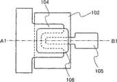
图1A和1B为在衬底101表面上方制造的薄膜晶体管的示例。图1A为薄膜晶体管的俯视图,而图1B为沿A1-B1线截取的截面图。1A and 1B are examples of thin film transistors fabricated over the surface of a
图1A和1B所示的薄膜晶体管具有底栅结构,其中栅电极102和栅绝缘层103被顺序地形成于衬底101上方且氧化物半导体层106被形成于栅绝缘层103上方。源电极104和漏电极105被配置于栅绝缘层103和氧化物半导体层106之间。换句话说,氧化物半导体层106被配置成与栅电极102重叠并且与栅绝缘层103的上部的一部分以及源电极104和漏电极105的上部和侧部的一部分相接触。源电极104和漏电极105在氧化物半导体层106之前被配置于栅绝缘层103上方的结构其优点在于,可以在底面上形成氧化物半导体层106之前利用等离子体处理来清洁底面。The thin film transistor shown in FIGS. 1A and 1B has a bottom gate structure in which a
栅电极102优选地由难熔金属诸如Ti、Mo、Cr、Ta、或W形成。替代地,栅电极102可以具有在Al膜的上方或者在添加了Si、Ti、Nd、Sc、或Cu等的Al膜的上方设置以Mo、Cr、或Ti为代表的难熔金属的层的结构。The
栅绝缘层103优选地由硅的氧化物或氮化物诸如氧化硅、氮化硅、或氧氮化硅形成。具体地,当栅绝缘层103由氧化硅形成时,源电极和栅电极之间的以及漏电极和栅电极之间的泄漏电流可以为10-10A或更低。这些绝缘层可以通过等离子体CVD法、或溅射法等形成。The
例如,作为栅绝缘层103,可以通过使用有机硅烷气体的CVD法形成氧化硅层。作为有机硅烷气体,可以使用含硅的化合物,诸如四乙氧基硅烷(TEOS)(化学式:Si(OC2H5)4)、四甲基硅烷(TMS)(化学式:Si(CH3)4)、四甲基环四硅氧烷(TMCTS)、八甲基环四硅氧烷(OMCTS)、六甲基二硅氮烷(HMDS)、三乙氧基硅烷(SiH(OC2H5)3)、或者三(二甲基氨基)硅烷(SiH(N(CH3)2)3)。For example, as the
源电极104和漏电极105优选地使用难熔金属诸如Ti、Mo、Cr、Ta、或W形成。具体地,优选地使用对氧具有高亲合力(affinity foroxygen)的金属材料,典型地是Ti。这是因为这种金属材料易于产生与氧化物半导体层106的欧姆接触。除了Ti,也可以使用Mo以得到类似效果。源电极104和漏电极105优选地被蚀刻加工以具有锥形端部(tapered end)形状。以此方式,可以增大它们与氧化物半导体层106的接触面积。在源电极和漏电极104和105与氧化物半导体膜之间,可以配置具有氧缺乏缺陷(oxygen-deficient defect)的氧化物半导体膜(电阻比沟道形成区的氧化物半导体膜的电阻低的氧化物半导体膜)。The
作为源电极104和漏电极105的另一个方式,电极可以具有这样的结构,其中以Mo、Cr、或Ti为代表的难熔金属的层被形成于Al膜上方和/或下方、或者被形成于添加了Si、Ti、Nd、Sc、或Cu等的Al膜的上方和/或下方。该结构在与用于形成源电极104和漏电极105的层同时并且用相同的层形成用于传输信号的布线时是优选的。优选地以与Al膜相接触的方式配置难熔金属层,以防止在Al膜上形成小丘(hillock)或晶须(whisker)。注意术语“小丘”是指这样的现象:当Al的晶体生长在进行时,生长成分相互碰撞(impinge)而形成隆起。术语“晶须”是指Al由于异常生长而生长成针状的现象。As another mode of the
利用以溅射法为代表的PVD法形成氧化物半导体层106。作为金属靶材,可以优选地使用上述的In、M(M为选自Ga、Fe、Ni、Mn、Co、和Al中的一种或多种元素)和Zn的氧化物的烧结体。例如氧化物半导体膜可以使用In2O3、Ga2O3、和ZnO的烧结体作为靶材,通过溅射法形成。The
作为溅射气体,使用以氩气为代表的稀有气体。为了控制氧化物半导体膜的氧缺乏缺陷,可以在稀有气体中加入预定量的氧气。通过增加溅射气体中氧气对稀有气体之比,可以减少氧化物半导体中的氧缺乏缺陷。控制氧化物半导体中的氧缺乏缺陷使得能够控制薄膜晶体管的阈值电压。As the sputtering gas, a rare gas typified by argon is used. In order to control oxygen deficient defects of the oxide semiconductor film, a predetermined amount of oxygen may be added to the rare gas. Oxygen deficiency defects in an oxide semiconductor can be reduced by increasing the ratio of oxygen to the rare gas in the sputtering gas. Controlling oxygen-deficiency defects in an oxide semiconductor enables control of the threshold voltage of a thin film transistor.
在形成氧化物半导体层106之前,优选地通过将氩气导入溅射装置的沉积室中并产生等离子体来进行处理以清洁沉积表面。替代氩气氛,可以使用氮、或氦等。替代地,上述处理可以在通过向氩气氛中加入氧、或N2O等而得到的气氛中进行。作为另一个选择,处理可以在通过向氩气氛中加入Cl2、或CF4等而得到的气氛中进行。Before forming the
在形成氧化物半导体层106之后,在空气或氮气氛中,在200℃到600℃下、优选在300℃到400℃下进行热处理。经过该热处理,可以提高薄膜晶体管的场效应迁移率。具有本实施方式所述的氧化物半导体的薄膜晶体管的场效应迁移率可以为5cm2/V·sec或更高。After the
当在上述的薄膜晶体管的源电极和漏电极之间施加约5V的电压、并且不对栅电极施加电压时,源电极和漏电极之间流动的电流可以为1×10-11A或更低。即使在对栅电极施加-10V的电压的状态下,源电极和漏电极之间流过的电流也为1×10-11A或更低。When a voltage of about 5 V is applied between the source electrode and the drain electrode of the thin film transistor described above and no voltage is applied to the gate electrode, the current flowing between the source electrode and the drain electrode may be 1×10⁻¹¹ A or less. Even when a voltage of -10V is applied to the gate electrode, the current flowing between the source electrode and the drain electrode is 1×10-11 A or less.
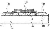
图2A和2B表示了在衬底101的表面上方制造的薄膜晶体管的示例。图2A为薄膜晶体管的俯视图,而图2B为沿A2-B2线截取的截面图。2A and 2B show an example of a thin film transistor fabricated over the surface of a
图2A和2B所示的薄膜晶体管具有底栅结构,其中栅电极102和栅绝缘层103被顺序地形成于衬底101上方且氧化物半导体层106被形成于栅绝缘层103上方。在该结构中,源电极104和漏电极105与氧化物半导体层106的侧表面和上表面相接触。The thin film transistor shown in FIGS. 2A and 2B has a bottom gate structure in which a
在具有这种结构的薄膜晶体管中,可以连续地形成栅绝缘层103、氧化物半导体层106、和用于形成源电极104和漏电极105的导电层。换句话说,这些层可以被层叠而不将栅绝缘层103和氧化物半导体层106之间的界面以及氧化物半导体层106和导电层之间的界面暴露于空气;因而,可以防止每个界面被污染。In a thin film transistor having such a structure, the
另外,可以通过执行蚀刻以去除氧化物半导体层106的暴露于源电极104和漏电极106之间的浅表(superficial)部分来减小截止电流。此外,通过在氧化物半导体层106的暴露部分或者在通过蚀刻去除所获得的表面上执行氧等离子体处理,可以提高暴露于等离子体的浅表部分的电阻。这是因为氧化物半导体中的氧缺乏缺陷被氧化,从而减小了载流子浓度(电子浓度)。通过该氧等离子体处理,可以降低薄膜晶体管的截止电流。In addition, off-current can be reduced by performing etching to remove a superficial portion of the
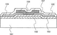
图3A和3B表示了在衬底101表面上方制造的薄膜晶体管的示例。图3A为薄膜晶体管的俯视图,而图3B为沿A3-B3线截取的截面图。3A and 3B show an example of a thin film transistor fabricated over the surface of a
图3A和3B所示的薄膜晶体管具有顶栅结构,其中源电极104和漏电极105、氧化物半导体层106、栅绝缘层103、和栅电极102被顺序地形成于衬底101之上。在如下情况下,可以降低薄膜晶体管的截止电流并提高其通断比,即、前述薄膜晶体管的氧化物半导体层106用由InMO3(ZnO)m(M是选自Ga、Fe、Ni、Mn、Co、和Al的一种或多种元素,且m为大于或等于1且小于50的非整数)表示的氧化物半导体材料形成并且具有下列组成:当In、M、Zn、和O的浓度总和被定义为100%时,含In的浓度小于20原子%,含M(例如Ga)的浓度小于20原子%,且含Zn的浓度小于10原子%。The thin film transistor shown in FIGS. 3A and 3B has a top gate structure in which a
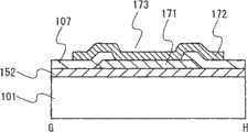
图4A表示了这样的示例,其中氧化物绝缘层107被配置于氧化物半导体层106上方,其与栅绝缘层103相对置(在背沟道(backchannel)一侧)。对于氧化物绝缘层107,可以使用氧化铝、氧氮化铝、氧化钇、或氧化铪,以及上述的氧化硅中的任何一种。利用图4A所示的氧化物半导体层106被夹在包含氧化硅的栅绝缘层103与氧化物绝缘层107之间的结构,可以防止由于从氧化物半导体层106中释放的氧而形成的氧缺乏缺陷。FIG. 4A shows an example in which an
图4B表示了这样的结构,其中氮化物绝缘层108被配置于氧化物绝缘层107上方。对于氮化物绝缘层108,可以使用氮化硅、或氮化铝等。利用氮化物绝缘层108,可以防止来自外部环境的水蒸汽、有机物、和离子金属(ionic metal)造成的污染。注意,在图4B的结构中,具有氮化硅层和氧化硅层的双层结构的栅绝缘层103也是有效的。在该情况中,氧化物半导体层106被夹在上方的氧化物和氮化物绝缘层与下方的氧化物和氮化物绝缘层之间;因而,可以进一步增强上述效果。FIG. 4B shows a structure in which a
(包括薄膜晶体管的装置)(devices including thin film transistors)
具有本实施方式所述的氧化物半导体的薄膜晶体管因为其高场效应迁移率和高通断比而可以被用于各多种应用。下面以显示装置的方式为例进行说明。A thin film transistor having the oxide semiconductor described in this embodiment mode can be used in various applications because of its high field-effect mobility and high on-off ratio. The method of the display device is taken as an example for description below.
图5表示了显示装置109,其中像素部分110、扫描线驱动电路111、和信号线一侧的选择器电路112被配置于衬底101上方。被配置于像素部分110、扫描线驱动电路111、和信号线一侧的选择器电路112中的开关元件包括每个的沟道形成区都被形成于氧化物半导体层中的薄膜晶体管。使用沟道形成区被形成于氧化物半导体层中且场效应迁移率为5cm2/V·sec到20cm2/V·sec的薄膜晶体管,可以形成扫描线驱动电路111和信号线一侧的选择器电路112。选择器电路112是在预定定时选择信号线116并将从驱动IC 114传输的视频信号分配给预定信号线116的电路。在本例中,薄膜晶体管是n沟道型的,因而扫描线驱动电路111和信号线一侧的选择器112包括n沟道薄膜晶体管。FIG. 5 shows a
在包括多个扫描线115和与扫描线115相交的多个信号线116的像素部分110中,配置有像素晶体管117。像素晶体管117被排列成矩阵。对于像素晶体管117,扫描信号经由扫描线115输入而视频信号经由信号线116输入。视频信号从驱动IC 114被输入到输入端子113。驱动IC 114被形成于单晶衬底上并通过带式自动接合(TAB)法或玻璃上芯片接合(COG)法安装。In the
图6表示了包括n沟道薄膜晶体管的选择器电路112的结构的示例。选择器电路112包括多个被排列的开关电路119。在每个开关电路119中,配置一个视频信号输入线120,而多个信号线116(S1到S3)延伸到像素部分110。开关电路119配置有数量与信号线116的数量相对应的开关元件121。当这些开关元件121包括每个的沟道形成区都被形成于氧化物半导体层中的薄膜晶体管时,开关电路119可以与视频信号的频率一致地高速工作。图6表示了开关电路119的示例,其中信号线116(S1)、信号线116(S2)、和信号线116(S3)分别配置有开关元件121a、开关元件121b、和开关元件121c。关于是导通还是关断开关元件121的判断是利用经由与视频信号输入线120不同路径的同步信号输入线122所输入的信号控制的。FIG. 6 shows an example of the structure of the
下面结合图7所示的时序图说明图6所示的选择器电路112的操作。作为示例,图7的时序图表示了第i行扫描线被选中并且给定列的视频信号输入线120被连接到选择器电路112的情况。第i行扫描线的选择期间被划分成第一子选择期间T1、第二子选择期间T2、和第三子选择期间T3。该时序图还表示了开关元件121a、开关元件121b、和开关元件121c导通或关断的定时和被输入到视频信号输入线120的信号。The operation of the
如图7所示,在第一子选择期间T1,开关元件121a导通而开关元件121b和开关元件121c关断。此时,输入到视频信号输入线120的视频信号VD(1)经由开关元件121a输出到信号线116(S1)。在第二子选择期间T2,开关元件121b导通而开关元件121a和开关元件121c关断,视频信号VD(2)经由开关元件121b输出到信号线116(S2)。在第三子选择期间T3,开关元件121c导通而开关元件121a和开关元件121b关断,视频信号VD(3)经由开关元件121c输出到信号线116(S3)。As shown in FIG. 7, during the first sub-selection period T1, the
通过将栅选择期间如上所述一分为三,图6的选择器电路112可以在一个栅选择期间经由一根视频信号输入线120将视频信号输入到三根信号线116(S1到S3)。这样,当选择器电路112和像素晶体管117一起被配置于衬底101上方时,被输入驱动IC信号的输入端子113的数量可以被减少到不配置选择器电路112的情况时的数量的1/3。因此,可以降低驱动IC和输入端子113之间发生接触缺陷的概率。By dividing the gate selection period into three as described above, the
扫描线驱动电路111还可以利用每个沟道形成区都被配置于氧化物半导体层中的薄膜晶体管来形成。扫描线驱动电路111包括移位寄存器作为部件。当时钟信号(CLK)和启动脉冲信号(SP)被输入到移位寄存器中时,生成选择信号。所生成的选择信号被缓冲器缓冲和放大,且所得的信号被提供给相应的扫描线115。一行的像素晶体管117的栅电极被连接到每根扫描线115。在此处,将结合图8和图9说明扫描线驱动电路111的一部分中所包括的移位寄存器123的模式。The scan
图8表示了移位寄存器123的结构。移位寄存器123包括被连接起来的多级触发器电路124。触发器电路124的示例如图9所示。图9所示的触发器电路124包括多个薄膜晶体管(在以下关于图9的说明中称为“TFT”)。图9所示的触发器电路124包括n沟道TFT,即TFT(1)125、TFT(2)126、TFT(3)127、TFT(4)128、TFT(5)129、TFT(6)130、TFT(7)131、和TFT(8)132。n沟道TFT在栅-源电压(Vgs)超过阈值电压(Vth)时导通。FIG. 8 shows the structure of the shift register 123. As shown in FIG. The shift register 123 includes multi-stage flip-flop circuits 124 connected together. An example of flip-flop circuit 124 is shown in FIG. 9 . The flip-flop circuit 124 shown in FIG. 9 includes a plurality of thin film transistors (referred to as “TFTs” in the following description about FIG. 9 ). The flip-flop circuit 124 shown in FIG. 9 includes n-channel TFTs, namely TFT (1) 125, TFT (2) 126, TFT (3) 127, TFT (4) 128, TFT (5) 129, TFT (6) 130, TFT (7) 131, and TFT (8) 132. An n-channel TFT is turned on when a gate-source voltage (Vgs) exceeds a threshold voltage (Vth).
注意,虽然此处在图9所示的触发器电路124中所包括的所有TFT都为增强型n沟道晶体管,但是,例如,如果将耗尽型n沟道晶体管用作TFT(3)127,驱动电路也可以被驱动。Note that although all TFTs included in the flip-flop circuit 124 shown in FIG. , the drive circuit can also be driven.
TFT(1)125的第一电极(源电极和漏电极中的一个)被连接到布线(4)136,TFT(1)125的第二电极(源电极和漏电极中的另一个)被连接到布线(3)135。The first electrode (one of the source electrode and the drain electrode) of the TFT (1) 125 is connected to the wiring (4) 136, and the second electrode (the other of the source electrode and the drain electrode) of the TFT (1) 125 is connected to wiring (3)135.
TFT(2)126的第一电极被连接到布线(6)138,TFT(2)126的第二电极被连接到布线(3)135。The first electrode of the TFT ( 2 ) 126 is connected to the wiring ( 6 ) 138 , and the second electrode of the TFT ( 2 ) 126 is connected to the wiring ( 3 ) 135 .
TFT(3)127的第一电极被连接到布线(5)137;TFT(3)127的第二电极被连接到TFT(2)126的栅电极;而TFT(3)127的栅电极被连接到布线(5)137。The first electrode of TFT (3) 127 is connected to wiring (5) 137; the second electrode of TFT (3) 127 is connected to the gate electrode of TFT (2) 126; And the gate electrode of TFT (3) 127 is connected to route (5)137.
TFT(4)128的第一电极被连接到布线(6)138;TFT(4)128的第二电极被连接到TFT(2)126的栅电极;而TFT(4)128的栅电极被连接到TFT(1)125的栅电极。The first electrode of TFT (4) 128 is connected to wiring (6) 138; the second electrode of TFT (4) 128 is connected to the gate electrode of TFT (2) 126; And the gate electrode of TFT (4) 128 is connected to the gate electrode of the TFT (1) 125 .
TFT(5)129的第一电极被连接到布线(5)137;TFT(5)129的第二电极被连接到TFT(1)125的栅电极;而TFT(5)129的栅电极被连接到布线(1)133。The first electrode of TFT (5) 129 is connected to wiring (5) 137; the second electrode of TFT (5) 129 is connected to the gate electrode of TFT (1) 125; And the gate electrode of TFT (5) 129 is connected to wiring (1)133.
TFT(6)130的第一电极被连接到布线(6)138;TFT(6)130的第二电极被连接到TFT(1)125的栅电极;而TFT(6)130的栅电极被连接到TFT(2)126的栅电极。The first electrode of TFT (6) 130 is connected to wiring (6) 138; the second electrode of TFT (6) 130 is connected to the gate electrode of TFT (1) 125; And the gate electrode of TFT (6) 130 is connected to the gate electrode of TFT (2) 126 .
TFT(7)131的第一电极被连接到布线(6)138;TFT(7)131的第二电极被连接到TFT(1)125的栅电极;而TFT(7)131的栅电极被连接到布线(2)134。TFT(8)132的第一电极被连接到布线(6)138;TFT(8)132的第二电极被连接到TFT(2)126的栅电极;而TFT(8)132的栅电极被连接到布线(1)133。The first electrode of TFT (7) 131 is connected to wiring (6) 138; the second electrode of TFT (7) 131 is connected to the gate electrode of TFT (1) 125; And the gate electrode of TFT (7) 131 is connected to route (2)134. The first electrode of TFT (8) 132 is connected to wiring (6) 138; the second electrode of TFT (8) 132 is connected to the gate electrode of TFT (2) 126; And the gate electrode of TFT (8) 132 is connected to wiring (1)133.
沟道形成区被配置于氧化物半导体层中的薄膜晶体管具有高场效应迁移率,因而其工作频率可以被设得高。另外,因为薄膜晶体管的频率特性高,所以扫描线驱动电路111可以高速工作,且显示装置可以以高帧频工作。A thin film transistor in which a channel formation region is arranged in an oxide semiconductor layer has high field effect mobility, and thus its operating frequency can be set high. In addition, since the frequency characteristic of the thin film transistor is high, the scanning
在图5中,像素部分110的结构随显示介质118的不同而变化。当显示介质118是在电极之间夹着液晶材料的液晶元件时,显示介质118可以如图5所示由像素晶体管117控制。在一对电极之间夹着显影介质(电子墨水或者电泳材料)的显示介质118的情况同样适用。可以通过与上述驱动电路组合来操作包括这些显示介质118的像素部分110。In FIG. 5 , the structure of the
当被用作显示介质118时,使用电致发光材料形成的发光元件比液晶元件更适合于时间灰度法,因为其响应速度高于液晶元件等的响应速度。例如在利用时间灰度法进行显示的情况中,一个帧期间被划分成多个子帧期间。然后,根据视频信号,发光元件在每个子帧期间中被设定为发光态或非发光态。通过将一个帧期间划分成多个子帧期间,可以用视频信号控制像素在一个帧期间中实际发光的时间的总长度,从而可以显示灰度。When used as the
在像素部分110包括发光元件的情况下的像素的示例如图10所示。图10表示了可以采用数字时间灰度驱动法的像素结构。此处所述为这样的示例,其中,每个的沟道形成区都使用氧化物半导体层而形成的两个n沟道薄膜晶体管被包括在一个像素中。An example of a pixel in the case where the
像素139包括开关TFT 140、驱动TFT 141、发光元件142、和电容145。开关TFT 140的栅极被连接到扫描线115;开关TFT 140的第一电极(源电极和漏电极中的一个)被连接到信号线116;且开关TFT 140的第二电极(源电极和漏电极中的另一个)被连接到驱动TFT 141的栅极。驱动TFT 141的栅极经由电容145被连接到电源线146;驱动TFT 141的第一电极被连接到电源线146;且驱动TFT 141的第二电极被连接到发光元件142的第一电极(像素电极)143。发光元件142的第二电极(对置电极)144被连接到公共电位线147。The
发光元件142的第二电极(对置电极)144被设为低电源电位。注意,低电源电位是指基于对电源线146所设的高电源电位满足以下方程的电位:(低电源电位)<(高电源电位)。作为低电源电位,例如可以采用GND、或0V等。为了通过将高电源电位和低电源电位之间的电位差施加到发光元件142从而将电流供给到发光元件142而使发光元件142发光,每个电位都被设定使得高电源电位和低电源电位之间的电位差等于或高于发光元件142的正向阈值电压。The second electrode (counter electrode) 144 of the
在电压输入电压驱动法(voltage-input voltage driving method)的情况中,视频信号被输入到驱动TFT 141的栅极使得驱动TFT 141处于被充分地导通和关断这两个状态中的某一个状态。即,驱动TFT141工作在线性区。比电源线146电压更高的电压被施加到驱动TFT141的栅极使得驱动TFT 141工作在线性区。注意,比由方程(电源线的电压)+(驱动TFT 141的阈值电压)所表示的电压更高或相等的电压被施加到信号线116。In the case of a voltage-input voltage driving method, a video signal is input to the gate of the driving
替代数字时间灰度驱动法,模拟灰度驱动法也可以被应用于图10所示的像素结构。在进行模拟灰度驱动的情况中,比由方程(发光元件142的正向电压)+(驱动TFT 141的阈值电压)所表示的电压更高或相等的电压被施加到驱动TFT 141的栅极。发光元件142的正向电压是指要获得所需照明所需的电压,并且至少包括正向阈值电压。注意,当输入使驱动TFT 141工作在饱和区的视频信号时,电流可以被供给到发光元件142。电源线146的电位被设定得高于驱动TFT 141的栅电位,使驱动TFT 141工作在饱和区。当视频信号为模拟信号时,能够将符合视频信号的电流供给到发光元件142并进行模拟灰度驱动。Instead of the digital time grayscale driving method, the analog grayscale driving method can also be applied to the pixel structure shown in FIG. 10 . In the case of performing analog gradation driving, a voltage higher than or equal to the voltage represented by the equation (forward voltage of the light emitting element 142)+(threshold voltage of the driving TFT 141) is applied to the gate of the driving
虽然图10表示了对发光元件142的驱动进行控制的驱动TFT141被电连接到发光元件的示例,但是可以采用在驱动TFT 141和发光元件142之间连接电流控制TFT的结构。Although FIG. 10 shows an example in which the driving
虽然图5表示了配置有用于选择信号线116的选择器电路112的显示装置109的示例,但是当薄膜晶体管具有10cm/V·sec或更高的场效应迁移率时,可以利用使用了用于沟道形成区的氧化物半导体层形成的薄膜晶体管来实现驱动IC 114的功能。即,可以利用每个都使用用于沟道形成区的氧化物半导体层形成的薄膜晶体管,在衬底101上方形成扫描线驱动电路和信号线驱动电路。Although FIG. 5 shows an example of the
(发光装置)(light emitting device)
下面结合图11以及图12A和12B说明作为显示装置的一种方式的发光装置的像素结构。图11是像素的俯视图的示例;图12A为沿C1-D1线截取的截面图;而图12B为沿C2-D2线截取的截面图。在下列说明中,参考图11以及图12A和12B。注意,图11所示像素的等效电路与图10所示类似。The pixel structure of a light-emitting device as one form of a display device will be described below with reference to FIG. 11 and FIGS. 12A and 12B . 11 is an example of a plan view of a pixel; FIG. 12A is a cross-sectional view taken along line C1-D1; and FIG. 12B is a cross-sectional view taken along line C2-D2. In the following description, reference is made to FIG. 11 and FIGS. 12A and 12B. Note that the equivalent circuit of the pixel shown in FIG. 11 is similar to that shown in FIG. 10 .
开关TFT 140的沟道形成区被形成于氧化物半导体层153中。氧化物半导体层153类似于本实施方式所述的氧化物半导体层。开关TFT 140具有用与扫描线115相同的层形成的栅电极148,且氧化物半导体层153被配置于栅绝缘层152上方。氧化物半导体层153与利用与信号线116相同的层形成于栅绝缘层152上方的源/漏电极155和源/漏电极156相接触。源/漏电极156经由配置于栅绝缘层152中的接触孔159而被连接到驱动TFT 141的栅电极149。A channel formation region of the switching
注意,术语“源/漏电极”是指被配置在包括源极、漏极、和栅极作为主要部件的薄膜晶体管中的用作源极或漏极的部分处的电极。Note that the term "source/drain electrode" refers to an electrode arranged at a portion serving as a source or a drain in a thin film transistor including a source, a drain, and a gate as main components.
信号线116、源/漏电极155、和源/漏电极156优选地用Al膜或者添加有Si、Ti、Nd、Sc、或Cu等的Al膜形成,从而可以降低布线或电极的电阻。以Mo、Cr、或Ti为代表的难熔金属的层被优选地配置于Al膜的上方和/或下方,从而防止在Al膜上产生小丘或晶须。The
栅电极149还起着电容145的电容电极150的作用。通过层叠电容电极150、栅绝缘层152、和由与电源线146相同的层形成的电容电极151来形成电容145。The
驱动TFT 141的栅电极149用与扫描线115相同的层形成,且氧化物半导体层154被配置于栅绝缘层152上方。氧化物半导体层154与利用与电源线146相同的层形成于栅绝缘层152上方的源/漏电极157和源/漏电极158相接触。The
氧化物绝缘层107被配置于氧化物半导体层153和氧化物半导体层154上方。第一电极(像素电极)143被配置于氧化物绝缘层107上方。第一电极(像素电极)143和源/漏电极158经由配置于氧化物绝缘层107中的接触孔160而被相互连接。利用无机绝缘材料或有机绝缘材料形成具有到第一电极(像素电极)143的开口的分隔层(partition layer)161。形成分隔层161使得其在开口处的端部具有平缓曲面。The
发光元件142具有这样的结构,其中EL层162被配置于第一电极(像素电极)143和第二电极(对置电极)144之间。第一电极(像素电极)143和第二电极(对置电极)144中的一个为空穴注入电极;而另一个为电子注入电极。空穴注入电极优选地利用功函数为4eV或更高的材料以及诸如含氧化钨的氧化铟、含氧化钨的氧化铟锌、含氧化钛的氧化铟、含氧化钛的氧化铟锡、氧化铟锡、氧化铟锌、或添加了氧化硅的氧化铟锡等材料来形成。电子注入电极优选地利用功函数低于4eV的材料形成,优选的是钙(Ca)、铝(Al)、氟化钙(CaF)、镁-银(MgAg)、或铝-锂(AlLi)等。EL层162是用于通过电致发光获得发光的层,是通过适当地组合载流子(空穴或电子)传输层和发光层而形成的。The
图13A到13C表示了发光装置的输入端子113的结构。图13A为输入端子113的俯视图。输入端子113被配置于衬底101的端部。沿图13A中G-H线截取的截面图如图13B或图13C所示。13A to 13C show the structure of the
图13B表示了用与扫描线115相同的层形成输入端子层170的示例。在输入端子层170上方层叠栅绝缘层152和氧化物绝缘层107,并在这些绝缘层中配置开口173从而经由绝缘层中的开口173暴露输入端子层170。用与输入端子层170相接触的透明导电膜172覆盖开口173。配置透明导电膜172以避免当柔性印刷布线(flexible printedwiring)和输入端子113被连接起来时的高接触电阻。由金属形成的输入端子层170的表面的氧化导致接触电阻的增加;在配置有由氧化物导电材料形成的透明导电膜172的情况下,可以防止接触电阻的增加。FIG. 13B shows an example in which the
图13C表示了利用与信号线116相同的层形成输入端子层171的示例。在输入终端层171上方配置氧化物绝缘层107,并在该绝缘层中配置开口173从而经由绝缘层中的开口173暴露输入端子层171。出于与上述相同的原因,配置透明导电薄膜172。FIG. 13C shows an example in which the
(显影介质显示装置)(Development medium display device)
图14表示了包括显影介质163的显示装置的一个方式(这种显示装置也被称为“电子纸”)。显影介质163与填充物164一起夹在第一电极(像素电极)143和第二电极(对置电极)144之间,并在电位差被施加于电极之间时改变对比度。第二电极(对置电极)144配置于对置衬底165上。FIG. 14 shows one form of a display device including a developing medium 163 (this kind of display device is also called "electronic paper"). The developing medium 163 is sandwiched between the first electrode (pixel electrode) 143 and the second electrode (counter electrode) 144 together with the filler 164, and changes the contrast when a potential difference is applied between the electrodes. The second electrode (counter electrode) 144 is disposed on the
例如,有一种被称为扭转球显示法的显示方法,其中在第一电极(像素电极)143和第二电极(对置电极)144之间放置每个都被着色成黑色和白色的球形颗粒,并且球形颗粒的取向受在电极之间所产生的电位差所控制。For example, there is a display method called a twisted ball display method in which spherical particles each colored in black and white are placed between a first electrode (pixel electrode) 143 and a second electrode (counter electrode) 144 , and the orientation of the spherical particles is controlled by the potential difference generated between the electrodes.
替代扭转球,也可以使用电泳元件。使用直径为约10μm到200μm的微囊,其中密封了透明填充物164、带正电的白色微粒、和带负电的黑色微粒。微囊被夹在第一电极(像素电极)143和第二电极(对置电极)144之间,而带正电的白色微粒和带负电的黑色微粒利用电极之间的电位差而分别在不同方向上移动。使用该原理的显示元件为电泳显示元件并且通常被称为电子纸。电泳显示元件的反射率高于液晶显示装置,因而不需要辅助光(auxiliary light)且功耗低,并且在暗处也可以识别显示部分。另外,即使不向显示部分供电,已经被显示过一次的图像也能被保持。因此,即使具有显示功能的半导体器件(其可以被简称为显示装置或配置有显示装置的半导体器件)远离电波源,所显示的图像也可以被存储。Instead of twisting balls, electrophoretic elements can also be used. Microcapsules with a diameter of about 10 μm to 200 μm in which transparent filler 164 , positively charged white particles, and negatively charged black particles are sealed are used. The microcapsules are sandwiched between the first electrode (pixel electrode) 143 and the second electrode (counter electrode) 144, and the positively charged white particles and negatively charged black particles utilize the potential difference between the electrodes to move at different levels, respectively. direction to move. A display element using this principle is an electrophoretic display element and is generally called electronic paper. The reflectance of the electrophoretic display element is higher than that of the liquid crystal display device, so that auxiliary light is not required and power consumption is low, and the display part can be recognized even in a dark place. In addition, even if power is not supplied to the display section, an image that has been displayed once can be held. Therefore, even if a semiconductor device having a display function (which may be simply referred to as a display device or a semiconductor device provided with a display device) is far away from an electric wave source, a displayed image can be stored.
(液晶显示装置)(Liquid Crystal Display Device)
下面结合图15以及图16说明作为显示装置的一种方式的液晶显示装置的像素结构。图15为像素的俯视图,而图16为沿E1-F1线截取的截面图。在下列说明中参考图15和图16。Next, a pixel structure of a liquid crystal display device as one form of a display device will be described with reference to FIGS. 15 and 16 . FIG. 15 is a top view of a pixel, and FIG. 16 is a cross-sectional view taken along line E1-F1. 15 and 16 are referred to in the following description.
图15和图16所示的液晶显示装置的像素包括被连接到扫描线115和信号线116的开关TFT 140。开关TFT 140的源/漏电极155被连接到信号线116,而其源/漏电极156经由配置于氧化物绝缘层107中的接触孔167被连接到第一电极(像素电极)143。电容145是通过层叠利用与栅电极148相同的层形成的电容线166、栅绝缘层152、和源/漏电极156而形成的。开关TFT 140控制对第一电极(像素电极)143的信号的输入。开关TFT 140的结构类似于图12A所示的结构。A pixel of the liquid crystal display device shown in FIGS. 15 and 16 includes a switching
液晶层169被配置于第一电极(像素电极)143和第二电极(对置电极)144之间。第一电极(像素电极)143被配置于氧化物绝缘层107上方。取向膜168被配置于第一电极(像素电极)143和第二电极(对置电极)144上。The
如上所述,可以利用沟道形成区被形成于如本实施方式所述的氧化物半导体层中的薄膜晶体管来实现具有优良的工作特性的显示装置。As described above, a display device having excellent operation characteristics can be realized using a thin film transistor in which a channel formation region is formed in the oxide semiconductor layer as described in this embodiment mode.
[实施例1][Example 1]
(氧化物半导体层的组成)(Composition of oxide semiconductor layer)
氧化物半导体层通过溅射法在下列条件下被形成于玻璃衬底之上。An oxide semiconductor layer was formed over a glass substrate by a sputtering method under the following conditions.
(条件1)(Condition 1)
靶材组成:In2O3∶Ga2O3∶ZnO=1∶1∶1Target composition: In2 O3 : Ga2 O3 : ZnO=1:1:1
(In∶Ga∶Zn=1∶1∶0.5)(In:Ga:Zn=1:1:0.5)
氩气流速:40sccmArgon flow rate: 40sccm
压力:0.4PaPressure: 0.4Pa
电功率(DC):500WElectric power (DC): 500W
衬底温度:室温Substrate temperature: room temperature
(条件2)(Condition 2)
靶材组成:In2O3∶Ga2O3∶ZnO=1∶1∶1Target composition: In2 O3 : Ga2 O3 : ZnO=1:1:1
(In∶Ga∶Zn=1∶1∶0.5)(In:Ga:Zn=1:1:0.5)
氩气流速:10sccmArgon flow rate: 10sccm
氧气流速:5sccmOxygen flow rate: 5sccm
压力:0.4PaPressure: 0.4Pa
电功率(DC):500WElectric power (DC): 500W
衬底温度:室温Substrate temperature: room temperature
在条件1和2下形成的氧化物半导体层通过感应耦合等离子体质谱法(ICP-MS)来评价。表1表示了测量的典型示例。在条件1下得到的氧化物半导体层具有由下列化学式表示的组成:InGa0.95Zn0.41O3.33。在条件2下得到的氧化物半导体层具有由下列化学式表示的组成:InGa0.94Zn0.40O3.31。The oxide semiconductor layers formed under
[表1][Table 1]

如上所述,ICP-MS的测量确认了在InMO3(ZnO)m中m为非整数。另外,成分的比例证明Zn的浓度低于In和Ga的浓度。As described above, measurement by ICP-MS confirmed that m is a non-integer in InMO3 (ZnO)m . In addition, the ratio of the components proves that the concentration of Zn is lower than that of In and Ga.
(氧化物半导体层的结构)(Structure of oxide semiconductor layer)
利用X光衍射来评价在上述条件2下在玻璃衬底上方所形成的厚度400nm的氧化物半导体层的结构。The structure of the oxide semiconductor layer having a thickness of 400 nm formed over the glass substrate under the
图17表示了在条件2下所形成的样品(刚被沉积后)的X光衍射图、在沉积之后在氮气氛中经受了一小时的350℃下的热处理的样品的X光衍射图、和在沉积之后在氮气氛中经受了一小时的500℃下的热处理的样品的X光衍射图。在所有样品中都观察到了光晕图案(halo pattern),这确认了样品具有非晶结构。17 shows the X-ray diffraction pattern of the sample formed under Condition 2 (just after being deposited), the X-ray diffraction pattern of the sample subjected to heat treatment at 350°C for one hour in a nitrogen atmosphere after deposition, and X-ray diffraction pattern of a sample subjected to heat treatment at 500° C. for one hour in a nitrogen atmosphere after deposition. A halo pattern was observed in all samples, confirming that the samples had an amorphous structure.
注意,当也用X光衍射评价用In2O3对Ga2O3和ZnO的组成比为1∶1∶2的靶材所形成的样品时,得到了类似的评价结果,这确认了本实施例中所形成的氧化物半导体层具有非晶结构。Note that similar evaluation results were obtained when a sample formed with a target having a composition ratio of In2 O3 to Ga2 O3 and ZnO of 1:1:2 was also evaluated by X-ray diffraction, confirming the The oxide semiconductor layer formed in Examples has an amorphous structure.
(薄膜晶体管的特性)(Characteristics of Thin Film Transistors)
图18表示了薄膜晶体管的栅极电压(Vg)-漏极电流(Id)特性。薄膜晶体管具有如图2A和2B所示的底栅结构,且沟道长度为100μm,沟道宽度为100μm。氧化物半导体层在上述条件2下形成。可以获得大于或等于15cm2/V·sec的场效应迁移率、小于或等于1×10-11A的截止电流、和大于或等于108的导通电流对截止电流之比(通断比)。如上所述,可以得到具有无法用传统薄膜晶体管得到的高通断比的薄膜晶体管。FIG. 18 shows gate voltage (Vg)-drain current (Id) characteristics of a thin film transistor. The thin film transistor has a bottom gate structure as shown in FIGS. 2A and 2B , and has a channel length of 100 μm and a channel width of 100 μm. The oxide semiconductor layer was formed under
本申请是基于2008年10月24日向日本专利局提交的第2008-274564号日本专利申请,其整体内容通过引用被并入本文中。This application is based on Japanese Patent Application No. 2008-274564 filed with Japan Patent Office on October 24, 2008, the entire contents of which are incorporated herein by reference.
Claims (24)
Translated fromChinesePriority Applications (1)
| Application Number | Priority Date | Filing Date | Title |
|---|---|---|---|
| CN201310338191.8ACN103474456B (en) | 2008-10-24 | 2009-10-23 | Oxide semiconductor, thin film transistor (TFT) and display device |
Applications Claiming Priority (2)
| Application Number | Priority Date | Filing Date | Title |
|---|---|---|---|
| JP2008274564AJP5442234B2 (en) | 2008-10-24 | 2008-10-24 | Semiconductor device and display device |
| JP2008-274564 | 2008-10-24 |
Related Child Applications (1)
| Application Number | Title | Priority Date | Filing Date |
|---|---|---|---|
| CN201310338191.8ADivisionCN103474456B (en) | 2008-10-24 | 2009-10-23 | Oxide semiconductor, thin film transistor (TFT) and display device |
Publications (2)
| Publication Number | Publication Date |
|---|---|
| CN101728424Atrue CN101728424A (en) | 2010-06-09 |
| CN101728424B CN101728424B (en) | 2013-09-11 |
Family
ID=42116609
Family Applications (2)
| Application Number | Title | Priority Date | Filing Date |
|---|---|---|---|
| CN201310338191.8AActiveCN103474456B (en) | 2008-10-24 | 2009-10-23 | Oxide semiconductor, thin film transistor (TFT) and display device |
| CN2009102070224AActiveCN101728424B (en) | 2008-10-24 | 2009-10-23 | Oxide semiconductor, thin film transistor, and display device |
Family Applications Before (1)
| Application Number | Title | Priority Date | Filing Date |
|---|---|---|---|
| CN201310338191.8AActiveCN103474456B (en) | 2008-10-24 | 2009-10-23 | Oxide semiconductor, thin film transistor (TFT) and display device |
Country Status (5)
| Country | Link |
|---|---|
| US (8) | US8878172B2 (en) |
| JP (1) | JP5442234B2 (en) |
| KR (8) | KR101686960B1 (en) |
| CN (2) | CN103474456B (en) |
| TW (7) | TWI697110B (en) |
Cited By (9)
| Publication number | Priority date | Publication date | Assignee | Title |
|---|---|---|---|---|
| WO2012097563A1 (en)* | 2011-01-18 | 2012-07-26 | 北京大学深圳研究生院 | Method of manufacturing thin film transistor |
| CN103050542A (en)* | 2012-12-28 | 2013-04-17 | 青岛润鑫伟业科贸有限公司 | Thin film transistor |
| CN104253215A (en)* | 2013-06-27 | 2014-12-31 | 海洋王照明科技股份有限公司 | Solar cell device and method for manufacturing same |
| CN106414366A (en)* | 2014-06-26 | 2017-02-15 | 住友金属矿山株式会社 | Oxide sintered body, sputtering target, and oxide semiconductor thin film using sputtering target |
| US9793801B2 (en) | 2010-05-21 | 2017-10-17 | Semiconductor Energy Laboratory Co., Ltd. | Semiconductor device and display device |
| CN111226307A (en)* | 2017-11-29 | 2020-06-02 | 株式会社神户制钢所 | Oxide semiconductor thin film, thin film transistor, and sputtering target |
| CN112018168A (en)* | 2019-05-30 | 2020-12-01 | 株式会社神户制钢所 | Oxide semiconductor thin films, thin film transistors and sputtering targets |
| CN112542545A (en)* | 2020-04-21 | 2021-03-23 | 友达光电股份有限公司 | Active component |
| CN116525577A (en)* | 2023-07-03 | 2023-08-01 | 合肥晶合集成电路股份有限公司 | A kind of semiconductor structure and its manufacturing method |
Families Citing this family (66)
| Publication number | Priority date | Publication date | Assignee | Title |
|---|---|---|---|---|
| WO2009110539A1 (en)* | 2008-03-06 | 2009-09-11 | 住友金属鉱山株式会社 | Semiconductor light emitting element, method for manufacturing the semiconductor light emitting element and lamp using the semiconductor light emitting element |
| EP2256814B1 (en) | 2009-05-29 | 2019-01-16 | Semiconductor Energy Laboratory Co, Ltd. | Oxide semiconductor device and method for manufacturing the same |
| KR101799252B1 (en) | 2009-07-31 | 2017-11-17 | 가부시키가이샤 한도오따이 에네루기 켄큐쇼 | Semiconductor device and method for manufacturing the same |
| KR102097932B1 (en) | 2009-07-31 | 2020-04-06 | 가부시키가이샤 한도오따이 에네루기 켄큐쇼 | Semiconductor device and manufacturing method thereof |
| KR101843558B1 (en) | 2009-10-09 | 2018-03-30 | 가부시키가이샤 한도오따이 에네루기 켄큐쇼 | Shift register and display device and driving method thereof |
| KR101812683B1 (en)* | 2009-10-21 | 2017-12-27 | 가부시키가이샤 한도오따이 에네루기 켄큐쇼 | Method for manufacturing semiconductor device |
| KR101849321B1 (en)* | 2009-11-06 | 2018-04-16 | 가부시키가이샤 한도오따이 에네루기 켄큐쇼 | Semiconductor device and manufacturing method thereof |
| WO2011070929A1 (en) | 2009-12-11 | 2011-06-16 | Semiconductor Energy Laboratory Co., Ltd. | Semiconductor device and electronic device |
| KR20190093706A (en)* | 2010-01-24 | 2019-08-09 | 가부시키가이샤 한도오따이 에네루기 켄큐쇼 | Display device and manufacturing method thereof |
| KR102838177B1 (en) | 2010-02-26 | 2025-07-23 | 가부시키가이샤 한도오따이 에네루기 켄큐쇼 | Liquid crystal display device |
| CN102893315B (en)* | 2010-05-11 | 2014-01-22 | 夏普株式会社 | Active matrix substrate and display panel |
| CN102906881B (en)* | 2010-05-21 | 2016-02-10 | 株式会社半导体能源研究所 | Semiconductor device |
| KR102615409B1 (en) | 2010-05-21 | 2023-12-20 | 가부시키가이샤 한도오따이 에네루기 켄큐쇼 | Pulse output circuit, shift register, and display device |
| WO2011145468A1 (en)* | 2010-05-21 | 2011-11-24 | Semiconductor Energy Laboratory Co., Ltd. | Memory device and semiconductor device |
| KR101872188B1 (en) | 2010-05-21 | 2018-06-29 | 가부시키가이샤 한도오따이 에네루기 켄큐쇼 | Semiconductor device and display device |
| WO2011155295A1 (en)* | 2010-06-10 | 2011-12-15 | Semiconductor Energy Laboratory Co., Ltd. | Dc/dc converter, power supply circuit, and semiconductor device |
| KR20120000499A (en) | 2010-06-25 | 2012-01-02 | 가부시키가이샤 한도오따이 에네루기 켄큐쇼 | Transistors and Semiconductor Devices |
| JP2012064201A (en)* | 2010-08-19 | 2012-03-29 | Semiconductor Energy Lab Co Ltd | Input-output device and driving method for input-output device |
| US8603841B2 (en)* | 2010-08-27 | 2013-12-10 | Semiconductor Energy Laboratory Co., Ltd. | Manufacturing methods of semiconductor device and light-emitting display device |
| JP5674594B2 (en)* | 2010-08-27 | 2015-02-25 | 株式会社半導体エネルギー研究所 | Semiconductor device and driving method of semiconductor device |
| TWI405335B (en) | 2010-09-13 | 2013-08-11 | Au Optronics Corp | Semiconductor structure and method of manufacturing same |
| US8792260B2 (en)* | 2010-09-27 | 2014-07-29 | Semiconductor Energy Laboratory Co., Ltd. | Rectifier circuit and semiconductor device using the same |
| CN103500712B (en)* | 2010-12-03 | 2016-05-25 | 株式会社半导体能源研究所 | Semiconductor device |
| US9202822B2 (en)* | 2010-12-17 | 2015-12-01 | Semiconductor Energy Laboratory Co., Ltd. | Semiconductor device and manufacturing method thereof |
| US8921948B2 (en)* | 2011-01-12 | 2014-12-30 | Semiconductor Energy Laboratory Co., Ltd. | Semiconductor device and manufacturing method thereof |
| TWI569041B (en) | 2011-02-14 | 2017-02-01 | 半導體能源研究所股份有限公司 | Display device |
| KR101555113B1 (en)* | 2011-02-28 | 2015-09-22 | 샤프 가부시키가이샤 | Semiconductor device and process of producing same, and display device |
| JP5490314B2 (en)* | 2011-04-18 | 2014-05-14 | シャープ株式会社 | Thin film transistor, display panel, and method of manufacturing thin film transistor |
| US9614094B2 (en)* | 2011-04-29 | 2017-04-04 | Semiconductor Energy Laboratory Co., Ltd. | Semiconductor device including oxide semiconductor layer and method for driving the same |
| CN102629574A (en)* | 2011-08-22 | 2012-08-08 | 京东方科技集团股份有限公司 | Oxide TFT array substrate and manufacturing method thereof and electronic device |
| JP5564026B2 (en)* | 2011-10-18 | 2014-07-30 | 株式会社フジクラ | Optical fiber tape core and optical fiber cable storing the optical fiber core |
| JP6076038B2 (en) | 2011-11-11 | 2017-02-08 | 株式会社半導体エネルギー研究所 | Method for manufacturing display device |
| JP6122275B2 (en) | 2011-11-11 | 2017-04-26 | 株式会社半導体エネルギー研究所 | Display device |
| US8796682B2 (en) | 2011-11-11 | 2014-08-05 | Semiconductor Energy Laboratory Co., Ltd. | Method for manufacturing a semiconductor device |
| US8956929B2 (en) | 2011-11-30 | 2015-02-17 | Semiconductor Energy Laboratory Co., Ltd. | Method for manufacturing semiconductor device |
| JP6059566B2 (en) | 2012-04-13 | 2017-01-11 | 株式会社半導体エネルギー研究所 | Method for manufacturing semiconductor device |
| JP6227890B2 (en) | 2012-05-02 | 2017-11-08 | 株式会社半導体エネルギー研究所 | Signal processing circuit and control circuit |
| US8995607B2 (en) | 2012-05-31 | 2015-03-31 | Semiconductor Energy Laboratory Co., Ltd. | Pulse signal output circuit and shift register |
| KR102343715B1 (en) | 2012-07-20 | 2021-12-27 | 가부시키가이샤 한도오따이 에네루기 켄큐쇼 | Semiconductor device and method for manufacturing semiconductor device |
| CN108054175A (en) | 2012-08-03 | 2018-05-18 | 株式会社半导体能源研究所 | Semiconductor device |
| DE102013216824B4 (en) | 2012-08-28 | 2024-10-17 | Semiconductor Energy Laboratory Co., Ltd. | semiconductor device |
| TWI611511B (en) | 2012-08-31 | 2018-01-11 | 半導體能源研究所股份有限公司 | Semiconductor device |
| CN104620390A (en) | 2012-09-13 | 2015-05-13 | 株式会社半导体能源研究所 | Semiconductor device |
| KR102021028B1 (en)* | 2012-12-04 | 2019-09-16 | 삼성디스플레이 주식회사 | Organic light emitting display device |
| KR102680781B1 (en)* | 2012-12-25 | 2024-07-04 | 가부시키가이샤 한도오따이 에네루기 켄큐쇼 | Semiconductor device |
| US9905585B2 (en) | 2012-12-25 | 2018-02-27 | Semiconductor Energy Laboratory Co., Ltd. | Semiconductor device comprising capacitor |
| KR20140125181A (en)* | 2013-04-18 | 2014-10-28 | 삼성디스플레이 주식회사 | Back palne of flat panel display and manufacturing method for the same |
| WO2014178422A1 (en)* | 2013-05-02 | 2014-11-06 | 富士フイルム株式会社 | Etching solution and etching solution kit, etching method using same, and production method for semiconductor substrate product |
| US9231002B2 (en) | 2013-05-03 | 2016-01-05 | Semiconductor Energy Laboratory Co., Ltd. | Display device and electronic device |
| TWI809474B (en) | 2013-05-16 | 2023-07-21 | 日商半導體能源研究所股份有限公司 | Semiconductor device |
| KR101636146B1 (en)* | 2014-09-16 | 2016-07-07 | 한양대학교 산학협력단 | Thin film transistor, and method of fabricating the same |
| CN105355604B (en)* | 2015-10-12 | 2018-04-20 | 深超光电(深圳)有限公司 | Thin-film transistor array base-plate |
| US10332446B2 (en)* | 2015-12-03 | 2019-06-25 | Innolux Corporation | Driving circuit of active-matrix organic light-emitting diode with hybrid transistors |
| KR102656977B1 (en)* | 2016-05-20 | 2024-04-12 | 가부시키가이샤 한도오따이 에네루기 켄큐쇼 | Semiconductor device or display device including the same |
| TWI778959B (en) | 2017-03-03 | 2022-10-01 | 日商半導體能源硏究所股份有限公司 | Semiconductor device and method for manufacturing the same |
| JP6844845B2 (en) | 2017-05-31 | 2021-03-17 | 三国電子有限会社 | Display device |
| JP7190729B2 (en) | 2018-08-31 | 2022-12-16 | 三国電子有限会社 | ORGANIC ELECTROLUMINESCENT DEVICE HAVING CARRIER INJECTION CONTROL ELECTRODE |
| JP7246681B2 (en) | 2018-09-26 | 2023-03-28 | 三国電子有限会社 | TRANSISTOR, TRANSISTOR MANUFACTURING METHOD, AND DISPLAY DEVICE INCLUDING TRANSISTOR |
| KR102698154B1 (en)* | 2019-12-31 | 2024-08-22 | 엘지디스플레이 주식회사 | Thin film transistor and display apparatus comprising the same |
| JP7444436B2 (en) | 2020-02-05 | 2024-03-06 | 三国電子有限会社 | liquid crystal display device |
| US11502110B2 (en) | 2020-03-18 | 2022-11-15 | Samsung Display Co., Ltd. | Display device and method of manufacturing the same |
| KR102774516B1 (en) | 2020-03-20 | 2025-03-05 | 삼성디스플레이 주식회사 | Display device |
| KR20210138826A (en) | 2020-05-12 | 2021-11-22 | 삼성디스플레이 주식회사 | Display device and method of fabricating the same |
| CN112530978B (en)* | 2020-12-01 | 2024-02-13 | 京东方科技集团股份有限公司 | Switching device structure and preparation method thereof, thin film transistor film layer, display panel |
| JP2023041449A (en)* | 2021-09-13 | 2023-03-24 | 株式会社Joled | Display device |
| WO2023189003A1 (en)* | 2022-03-30 | 2023-10-05 | 株式会社ジャパンディスプレイ | Thin film transistor and electronic device |
Family Cites Families (195)
| Publication number | Priority date | Publication date | Assignee | Title |
|---|---|---|---|---|
| JPS587537A (en) | 1981-07-06 | 1983-01-17 | Hitachi Zosen Corp | Method and device for detecting operation of internal combustion engine |
| JPS60198861A (en) | 1984-03-23 | 1985-10-08 | Fujitsu Ltd | Thin film transistor |
| JPH0244256B2 (en) | 1987-01-28 | 1990-10-03 | Kagaku Gijutsucho Mukizaishitsu Kenkyushocho | INGAZN2O5DESHIMESARERUROTSUHOSHOKEINOSOJOKOZOOJUSURUKAGOBUTSUOYOBISONOSEIZOHO |
| JPS63210023A (en) | 1987-02-24 | 1988-08-31 | Natl Inst For Res In Inorg Mater | Compound having a hexagonal layered structure represented by InGaZn↓4O↓7 and its manufacturing method |
| JPH0244258B2 (en) | 1987-02-24 | 1990-10-03 | Kagaku Gijutsucho Mukizaishitsu Kenkyushocho | INGAZN3O6DESHIMESARERUROTSUHOSHOKEINOSOJOKOZOOJUSURUKAGOBUTSUOYOBISONOSEIZOHO |
| JPH0244260B2 (en) | 1987-02-24 | 1990-10-03 | Kagaku Gijutsucho Mukizaishitsu Kenkyushocho | INGAZN5O8DESHIMESARERUROTSUHOSHOKEINOSOJOKOZOOJUSURUKAGOBUTSUOYOBISONOSEIZOHO |
| JPH0244262B2 (en) | 1987-02-27 | 1990-10-03 | Kagaku Gijutsucho Mukizaishitsu Kenkyushocho | INGAZN6O9DESHIMESARERUROTSUHOSHOKEINOSOJOKOZOOJUSURUKAGOBUTSUOYOBISONOSEIZOHO |
| JPH0244263B2 (en) | 1987-04-22 | 1990-10-03 | Kagaku Gijutsucho Mukizaishitsu Kenkyushocho | INGAZN7O10DESHIMESARERUROTSUHOSHOKEINOSOJOKOZOOJUSURUKAGOBUTSUOYOBISONOSEIZOHO |
| EP0445535B1 (en)* | 1990-02-06 | 1995-02-01 | Sel Semiconductor Energy Laboratory Co., Ltd. | Method of forming an oxide film |
| JP2585118B2 (en) | 1990-02-06 | 1997-02-26 | 株式会社半導体エネルギー研究所 | Method for manufacturing thin film transistor |
| JPH05251705A (en) | 1992-03-04 | 1993-09-28 | Fuji Xerox Co Ltd | Thin-film transistor |
| JP3587537B2 (en)* | 1992-12-09 | 2004-11-10 | 株式会社半導体エネルギー研究所 | Semiconductor device |
| JP3479375B2 (en) | 1995-03-27 | 2003-12-15 | 科学技術振興事業団 | Metal oxide semiconductor device in which a pn junction is formed with a thin film transistor made of a metal oxide semiconductor such as cuprous oxide, and methods for manufacturing the same |
| KR100394896B1 (en) | 1995-08-03 | 2003-11-28 | 코닌클리케 필립스 일렉트로닉스 엔.브이. | A semiconductor device including a transparent switching element |
| US5847410A (en)* | 1995-11-24 | 1998-12-08 | Semiconductor Energy Laboratory Co. | Semiconductor electro-optical device |
| JP3625598B2 (en) | 1995-12-30 | 2005-03-02 | 三星電子株式会社 | Manufacturing method of liquid crystal display device |
| JP2921510B2 (en) | 1996-10-07 | 1999-07-19 | 日本電気株式会社 | Bootstrap circuit |
| JP4170454B2 (en) | 1998-07-24 | 2008-10-22 | Hoya株式会社 | Article having transparent conductive oxide thin film and method for producing the same |
| EP0984492A3 (en)* | 1998-08-31 | 2000-05-17 | Sel Semiconductor Energy Laboratory Co., Ltd. | Semiconductor device comprising organic resin and process for producing semiconductor device |
| JP2000150861A (en) | 1998-11-16 | 2000-05-30 | Tdk Corp | Oxide thin film |
| JP3276930B2 (en) | 1998-11-17 | 2002-04-22 | 科学技術振興事業団 | Transistor and semiconductor device |
| US6909114B1 (en) | 1998-11-17 | 2005-06-21 | Semiconductor Energy Laboratory Co., Ltd. | Semiconductor device having LDD regions |
| JP2001053283A (en) | 1999-08-12 | 2001-02-23 | Semiconductor Energy Lab Co Ltd | Semiconductor device and manufacturing method thereof |
| TW460731B (en) | 1999-09-03 | 2001-10-21 | Ind Tech Res Inst | Electrode structure and production method of wide viewing angle LCD |
| JP2001109014A (en) | 1999-10-05 | 2001-04-20 | Hitachi Ltd | Active matrix type liquid crystal display |
| JP4089858B2 (en) | 2000-09-01 | 2008-05-28 | 国立大学法人東北大学 | Semiconductor device |
| KR100726132B1 (en)* | 2000-10-31 | 2007-06-12 | 엘지.필립스 엘시디 주식회사 | Array substrate for liquid crystal display device and manufacturing method |
| KR20020038482A (en) | 2000-11-15 | 2002-05-23 | 모리시타 요이찌 | Thin film transistor array, method for producing the same, and display panel using the same |
| JP3997731B2 (en) | 2001-03-19 | 2007-10-24 | 富士ゼロックス株式会社 | Method for forming a crystalline semiconductor thin film on a substrate |
| JP2002289859A (en) | 2001-03-23 | 2002-10-04 | Minolta Co Ltd | Thin film transistor |
| JP4090716B2 (en)* | 2001-09-10 | 2008-05-28 | 雅司 川崎 | Thin film transistor and matrix display device |
| JP3925839B2 (en) | 2001-09-10 | 2007-06-06 | シャープ株式会社 | Semiconductor memory device and test method thereof |
| JP4164562B2 (en)* | 2002-09-11 | 2008-10-15 | 独立行政法人科学技術振興機構 | Transparent thin film field effect transistor using homologous thin film as active layer |
| WO2003040441A1 (en)* | 2001-11-05 | 2003-05-15 | Japan Science And Technology Agency | Natural superlattice homologous single crystal thin film, method for preparation thereof, and device using said single crystal thin film |
| KR100456373B1 (en) | 2001-12-31 | 2004-11-09 | 엘지.필립스 엘시디 주식회사 | An etchant to etching Cu or Cu/Ti metal layer |
| JP4083486B2 (en) | 2002-02-21 | 2008-04-30 | 独立行政法人科学技術振興機構 | Method for producing LnCuO (S, Se, Te) single crystal thin film |
| CN1445821A (en) | 2002-03-15 | 2003-10-01 | 三洋电机株式会社 | Forming method of ZnO film and ZnO semiconductor layer, semiconductor element and manufacturing method thereof |
| JP3933591B2 (en)* | 2002-03-26 | 2007-06-20 | 淳二 城戸 | Organic electroluminescent device |
| WO2005016643A1 (en) | 2002-04-30 | 2005-02-24 | Aerospace Composite Structures, Llc | Method of thermoforming frtp sandwich panels, thermoformed articles, modular container |
| US7339187B2 (en) | 2002-05-21 | 2008-03-04 | State Of Oregon Acting By And Through The Oregon State Board Of Higher Education On Behalf Of Oregon State University | Transistor structures |
| JP2004022625A (en) | 2002-06-13 | 2004-01-22 | Murata Mfg Co Ltd | Semiconductor device and method of manufacturing the semiconductor device |
| US7105868B2 (en) | 2002-06-24 | 2006-09-12 | Cermet, Inc. | High-electron mobility transistor with zinc oxide |
| US7135728B2 (en) | 2002-09-30 | 2006-11-14 | Nanosys, Inc. | Large-area nanoenabled macroelectronic substrates and uses therefor |
| US7102605B2 (en) | 2002-09-30 | 2006-09-05 | Nanosys, Inc. | Integrated displays using nanowire transistors |
| US7051945B2 (en) | 2002-09-30 | 2006-05-30 | Nanosys, Inc | Applications of nano-enabled large area macroelectronic substrates incorporating nanowires and nanowire composites |
| WO2004032193A2 (en) | 2002-09-30 | 2004-04-15 | Nanosys, Inc. | Large-area nanoenabled macroelectronic substrates and uses therefor |
| US7619562B2 (en) | 2002-09-30 | 2009-11-17 | Nanosys, Inc. | Phased array systems |
| JP2006501690A (en) | 2002-09-30 | 2006-01-12 | ナノシス・インコーポレイテッド | Applications of large-area macroelectronic substrates incorporating nano-enabled, nanowires and nanowire hybrids |
| US7067867B2 (en) | 2002-09-30 | 2006-06-27 | Nanosys, Inc. | Large-area nonenabled macroelectronic substrates and uses therefor |
| US7067843B2 (en) | 2002-10-11 | 2006-06-27 | E. I. Du Pont De Nemours And Company | Transparent oxide semiconductor thin film transistors |
| JP2004214434A (en) | 2003-01-06 | 2004-07-29 | Sharp Corp | Oxide semiconductor light emitting device and manufacturing method |
| JP2004228401A (en) | 2003-01-24 | 2004-08-12 | Sharp Corp | Oxide semiconductor light emitting device and method of manufacturing the same |
| JP4166105B2 (en) | 2003-03-06 | 2008-10-15 | シャープ株式会社 | Semiconductor device and manufacturing method thereof |
| JP2004273732A (en) | 2003-03-07 | 2004-09-30 | Sharp Corp | Active matrix substrate and manufacturing method thereof |
| JP4141309B2 (en) | 2003-04-15 | 2008-08-27 | シャープ株式会社 | Semiconductor device and manufacturing method thereof |
| JP4108633B2 (en) | 2003-06-20 | 2008-06-25 | シャープ株式会社 | THIN FILM TRANSISTOR, MANUFACTURING METHOD THEREOF, AND ELECTRONIC DEVICE |
| TW200511589A (en)* | 2003-07-25 | 2005-03-16 | Hewlett Packard Development Co | Transistor including a deposited channel region having a doped portion |
| US20050017244A1 (en) | 2003-07-25 | 2005-01-27 | Randy Hoffman | Semiconductor device |
| US7262463B2 (en) | 2003-07-25 | 2007-08-28 | Hewlett-Packard Development Company, L.P. | Transistor including a deposited channel region having a doped portion |
| WO2005048222A1 (en) | 2003-11-14 | 2005-05-26 | Semiconductor Energy Laboratory Co., Ltd. | Light emitting display device, method for manufacturing the same, and tv set |
| KR100611152B1 (en)* | 2003-11-27 | 2006-08-09 | 삼성에스디아이 주식회사 | Flat Panel Display |
| US20050170643A1 (en)* | 2004-01-29 | 2005-08-04 | Semiconductor Energy Laboratory Co., Ltd. | Forming method of contact hole, and manufacturing method of semiconductor device, liquid crystal display device and EL display device |
| KR100625999B1 (en) | 2004-02-26 | 2006-09-20 | 삼성에스디아이 주식회사 | Donor sheet, manufacturing method of the donor sheet, manufacturing method of TFT using the donor sheet, and manufacturing method of flat panel display using the donor sheet |
| US7381579B2 (en) | 2004-02-26 | 2008-06-03 | Samsung Sdi Co., Ltd. | Donor sheet, method of manufacturing the same, method of manufacturing TFT using the donor sheet, and method of manufacturing flat panel display device using the donor sheet |
| US7282782B2 (en) | 2004-03-12 | 2007-10-16 | Hewlett-Packard Development Company, L.P. | Combined binary oxide semiconductor device |
| US7145174B2 (en) | 2004-03-12 | 2006-12-05 | Hewlett-Packard Development Company, Lp. | Semiconductor device |
| US7297977B2 (en) | 2004-03-12 | 2007-11-20 | Hewlett-Packard Development Company, L.P. | Semiconductor device |
| CN1998087B (en) | 2004-03-12 | 2014-12-31 | 独立行政法人科学技术振兴机构 | Amorphous oxide and thin film transistor |
| US7491590B2 (en)* | 2004-05-28 | 2009-02-17 | Semiconductor Energy Laboratory Co., Ltd. | Method for manufacturing thin film transistor in display device |
| KR101057891B1 (en) | 2004-05-31 | 2011-08-19 | 엘지디스플레이 주식회사 | Shift register |
| US7211825B2 (en) | 2004-06-14 | 2007-05-01 | Yi-Chi Shih | Indium oxide-based thin film transistors and circuits |
| JP2006100760A (en) | 2004-09-02 | 2006-04-13 | Casio Comput Co Ltd | Thin film transistor and manufacturing method thereof |
| US7285501B2 (en) | 2004-09-17 | 2007-10-23 | Hewlett-Packard Development Company, L.P. | Method of forming a solution processed device |
| US7298084B2 (en) | 2004-11-02 | 2007-11-20 | 3M Innovative Properties Company | Methods and displays utilizing integrated zinc oxide row and column drivers in conjunction with organic light emitting diodes |
| US7453065B2 (en) | 2004-11-10 | 2008-11-18 | Canon Kabushiki Kaisha | Sensor and image pickup device |
| US7829444B2 (en) | 2004-11-10 | 2010-11-09 | Canon Kabushiki Kaisha | Field effect transistor manufacturing method |
| EP2453481B1 (en)* | 2004-11-10 | 2017-01-11 | Canon Kabushiki Kaisha | Field effect transistor with amorphous oxide |
| AU2005302964B2 (en) | 2004-11-10 | 2010-11-04 | Canon Kabushiki Kaisha | Field effect transistor employing an amorphous oxide |
| KR100953596B1 (en) | 2004-11-10 | 2010-04-21 | 캐논 가부시끼가이샤 | Light emitting device |
| US7863611B2 (en) | 2004-11-10 | 2011-01-04 | Canon Kabushiki Kaisha | Integrated circuits utilizing amorphous oxides |
| US7791072B2 (en) | 2004-11-10 | 2010-09-07 | Canon Kabushiki Kaisha | Display |
| KR20060064264A (en) | 2004-12-08 | 2006-06-13 | 삼성전자주식회사 | Thin film transistor array panel and manufacturing method thereof |
| KR101110133B1 (en) | 2004-12-28 | 2012-02-20 | 엘지디스플레이 주식회사 | Shift register for LCD |
| US7579224B2 (en) | 2005-01-21 | 2009-08-25 | Semiconductor Energy Laboratory Co., Ltd. | Method for manufacturing a thin film semiconductor device |
| JP4777078B2 (en) | 2005-01-28 | 2011-09-21 | 株式会社半導体エネルギー研究所 | Method for manufacturing semiconductor device |
| TWI505473B (en) | 2005-01-28 | 2015-10-21 | Semiconductor Energy Lab | Semiconductor device, electronic device, and method of manufacturing semiconductor device |
| TWI445178B (en) | 2005-01-28 | 2014-07-11 | Semiconductor Energy Lab | Semiconductor device, electronic device, and method of manufacturing semiconductor device |
| US7858451B2 (en) | 2005-02-03 | 2010-12-28 | Semiconductor Energy Laboratory Co., Ltd. | Electronic device, semiconductor device and manufacturing method thereof |
| US7948171B2 (en) | 2005-02-18 | 2011-05-24 | Semiconductor Energy Laboratory Co., Ltd. | Light emitting device |
| US20060197092A1 (en) | 2005-03-03 | 2006-09-07 | Randy Hoffman | System and method for forming conductive material on a substrate |
| US8681077B2 (en) | 2005-03-18 | 2014-03-25 | Semiconductor Energy Laboratory Co., Ltd. | Semiconductor device, and display device, driving method and electronic apparatus thereof |
| US7544967B2 (en) | 2005-03-28 | 2009-06-09 | Massachusetts Institute Of Technology | Low voltage flexible organic/transparent transistor for selective gas sensing, photodetecting and CMOS device applications |
| US7645478B2 (en) | 2005-03-31 | 2010-01-12 | 3M Innovative Properties Company | Methods of making displays |
| US8300031B2 (en) | 2005-04-20 | 2012-10-30 | Semiconductor Energy Laboratory Co., Ltd. | Semiconductor device comprising transistor having gate and drain connected through a current-voltage conversion element |
| KR100647690B1 (en)* | 2005-04-22 | 2006-11-23 | 삼성에스디아이 주식회사 | Thin film transistor and flat panel display device having same |
| JP2006344849A (en) | 2005-06-10 | 2006-12-21 | Casio Comput Co Ltd | Thin film transistor |
| US7691666B2 (en) | 2005-06-16 | 2010-04-06 | Eastman Kodak Company | Methods of making thin film transistors comprising zinc-oxide-based semiconductor materials and transistors made thereby |
| US7402506B2 (en) | 2005-06-16 | 2008-07-22 | Eastman Kodak Company | Methods of making thin film transistors comprising zinc-oxide-based semiconductor materials and transistors made thereby |
| US7507618B2 (en) | 2005-06-27 | 2009-03-24 | 3M Innovative Properties Company | Method for making electronic devices using metal oxide nanoparticles |
| JP2007043113A (en) | 2005-06-30 | 2007-02-15 | Semiconductor Energy Lab Co Ltd | Semiconductor device and manufacturing method of semiconductor device |
| US7732330B2 (en) | 2005-06-30 | 2010-06-08 | Semiconductor Energy Laboratory Co., Ltd. | Semiconductor device and manufacturing method using an ink-jet method of the same |
| JP5036241B2 (en) | 2005-07-27 | 2012-09-26 | 株式会社半導体エネルギー研究所 | Method for manufacturing semiconductor device |
| US7655566B2 (en)* | 2005-07-27 | 2010-02-02 | Semiconductor Energy Laboratory Co., Ltd. | Method for manufacturing semiconductor device |
| KR100711890B1 (en) | 2005-07-28 | 2007-04-25 | 삼성에스디아이 주식회사 | OLED display and manufacturing method thereof |
| TWI485681B (en)* | 2005-08-12 | 2015-05-21 | Semiconductor Energy Lab | Display device |
| JP2007059128A (en) | 2005-08-23 | 2007-03-08 | Canon Inc | Organic EL display device and manufacturing method thereof |
| JP4870403B2 (en) | 2005-09-02 | 2012-02-08 | 財団法人高知県産業振興センター | Thin film transistor manufacturing method |
| JP4560502B2 (en) | 2005-09-06 | 2010-10-13 | キヤノン株式会社 | Field effect transistor |
| JP4880951B2 (en) | 2005-09-06 | 2012-02-22 | キヤノン株式会社 | Semiconductor device, thin film transistor, and thin film diode |
| JP5116225B2 (en) | 2005-09-06 | 2013-01-09 | キヤノン株式会社 | Manufacturing method of oxide semiconductor device |
| JP4850457B2 (en) | 2005-09-06 | 2012-01-11 | キヤノン株式会社 | Thin film transistor and thin film diode |
| JP4280736B2 (en) | 2005-09-06 | 2009-06-17 | キヤノン株式会社 | Semiconductor element |
| JP2007073705A (en)* | 2005-09-06 | 2007-03-22 | Canon Inc | Oxide semiconductor channel thin film transistor and method for manufacturing the same |
| JP5006598B2 (en)* | 2005-09-16 | 2012-08-22 | キヤノン株式会社 | Field effect transistor |
| JP5078246B2 (en) | 2005-09-29 | 2012-11-21 | 株式会社半導体エネルギー研究所 | Semiconductor device and manufacturing method of semiconductor device |
| JP5064747B2 (en)* | 2005-09-29 | 2012-10-31 | 株式会社半導体エネルギー研究所 | Semiconductor device, electrophoretic display device, display module, electronic device, and method for manufacturing semiconductor device |
| EP1770788A3 (en)* | 2005-09-29 | 2011-09-21 | Semiconductor Energy Laboratory Co., Ltd. | Semiconductor device having oxide semiconductor layer and manufacturing method thereof |
| JP4907942B2 (en) | 2005-09-29 | 2012-04-04 | シャープ株式会社 | Transistors and electronic devices |
| CN101283388B (en)* | 2005-10-05 | 2011-04-13 | 出光兴产株式会社 | TFT substrate and method for manufacturing TFT substrate |
| JP5142507B2 (en) | 2005-10-18 | 2013-02-13 | 株式会社半導体エネルギー研究所 | Semiconductor device, display device including the semiconductor device, and electronic apparatus |
| EP1777689B1 (en) | 2005-10-18 | 2016-08-10 | Semiconductor Energy Laboratory Co., Ltd. | Semiconductor device, and display device and electronic equipment each having the same |
| JP5037808B2 (en) | 2005-10-20 | 2012-10-03 | キヤノン株式会社 | Field effect transistor using amorphous oxide, and display device using the transistor |
| CN101577231B (en)* | 2005-11-15 | 2013-01-02 | 株式会社半导体能源研究所 | Semiconductor device and method of manufacturing the same |
| US7615495B2 (en) | 2005-11-17 | 2009-11-10 | Semiconductor Energy Laboratory Co., Ltd. | Display device and manufacturing method of the same |
| TWI292281B (en)* | 2005-12-29 | 2008-01-01 | Ind Tech Res Inst | Pixel structure of active organic light emitting diode and method of fabricating the same |
| US7867636B2 (en) | 2006-01-11 | 2011-01-11 | Murata Manufacturing Co., Ltd. | Transparent conductive film and method for manufacturing the same |
| JP4977478B2 (en)* | 2006-01-21 | 2012-07-18 | 三星電子株式会社 | ZnO film and method of manufacturing TFT using the same |
| US7576394B2 (en)* | 2006-02-02 | 2009-08-18 | Kochi Industrial Promotion Center | Thin film transistor including low resistance conductive thin films and manufacturing method thereof |
| US7977169B2 (en)* | 2006-02-15 | 2011-07-12 | Kochi Industrial Promotion Center | Semiconductor device including active layer made of zinc oxide with controlled orientations and manufacturing method thereof |
| JP2007272203A (en)* | 2006-03-06 | 2007-10-18 | Nec Corp | Display device |
| JP4930704B2 (en) | 2006-03-14 | 2012-05-16 | セイコーエプソン株式会社 | Organic electroluminescence device and electronic device |
| US7435633B2 (en) | 2006-03-14 | 2008-10-14 | Seiko Epson Corporation | Electroluminescence device, manufacturing method thereof, and electronic apparatus |
| JP5110803B2 (en) | 2006-03-17 | 2012-12-26 | キヤノン株式会社 | FIELD EFFECT TRANSISTOR USING OXIDE FILM FOR CHANNEL AND METHOD FOR MANUFACTURING THE SAME |
| KR20070101595A (en) | 2006-04-11 | 2007-10-17 | 삼성전자주식회사 | ZnO TFT |
| KR100763912B1 (en)* | 2006-04-17 | 2007-10-05 | 삼성전자주식회사 | Amorphous silicon thin film transistor and organic light emitting display having same |
| CN101060139A (en) | 2006-04-17 | 2007-10-24 | 三星电子株式会社 | Amorphous zinc oxide thin film transistor and method of manufacturing the same |
| KR100785038B1 (en) | 2006-04-17 | 2007-12-12 | 삼성전자주식회사 | Amorphous ZnO based Thin Film Transistor |
| US20070252928A1 (en)* | 2006-04-28 | 2007-11-01 | Toppan Printing Co., Ltd. | Structure, transmission type liquid crystal display, reflection type display and manufacturing method thereof |
| JP5250944B2 (en)* | 2006-04-28 | 2013-07-31 | 凸版印刷株式会社 | Structure, transmissive liquid crystal display device, semiconductor circuit manufacturing method, and transmissive liquid crystal display device manufacturing method |
| JP5135709B2 (en)* | 2006-04-28 | 2013-02-06 | 凸版印刷株式会社 | Thin film transistor and manufacturing method thereof |
| JP5124976B2 (en) | 2006-04-28 | 2013-01-23 | 凸版印刷株式会社 | Display device and manufacturing method thereof |
| JP4277874B2 (en) | 2006-05-23 | 2009-06-10 | エプソンイメージングデバイス株式会社 | Manufacturing method of electro-optical device |
| WO2007142167A1 (en)* | 2006-06-02 | 2007-12-13 | Kochi Industrial Promotion Center | Semiconductor device including an oxide semiconductor thin film layer of zinc oxide and manufacturing method thereof |
| US8330492B2 (en) | 2006-06-02 | 2012-12-11 | Semiconductor Energy Laboratory Co., Ltd. | Liquid crystal display device and electronic device |
| JP5028033B2 (en) | 2006-06-13 | 2012-09-19 | キヤノン株式会社 | Oxide semiconductor film dry etching method |
| KR101243809B1 (en)* | 2006-06-30 | 2013-03-18 | 엘지디스플레이 주식회사 | Method For Fabricating Thin Film Transistor And Method For Fabricating Thin Film Transistor Array Substrate By Applying Said Method |
| JP5062558B2 (en) | 2006-07-25 | 2012-10-31 | Nltテクノロジー株式会社 | Method for manufacturing active matrix substrate |
| JP4999400B2 (en) | 2006-08-09 | 2012-08-15 | キヤノン株式会社 | Oxide semiconductor film dry etching method |
| JP4609797B2 (en) | 2006-08-09 | 2011-01-12 | Nec液晶テクノロジー株式会社 | Thin film device and manufacturing method thereof |
| JP4952425B2 (en) | 2006-08-21 | 2012-06-13 | ソニー株式会社 | Liquid crystal device and electronic device |
| JP5127183B2 (en) | 2006-08-23 | 2013-01-23 | キヤノン株式会社 | Thin film transistor manufacturing method using amorphous oxide semiconductor film |
| JP4946286B2 (en) | 2006-09-11 | 2012-06-06 | 凸版印刷株式会社 | Thin film transistor array, image display device using the same, and driving method thereof |
| JP4332545B2 (en) | 2006-09-15 | 2009-09-16 | キヤノン株式会社 | Field effect transistor and manufacturing method thereof |
| JP5164357B2 (en) | 2006-09-27 | 2013-03-21 | キヤノン株式会社 | Semiconductor device and manufacturing method of semiconductor device |
| JP4274219B2 (en) | 2006-09-27 | 2009-06-03 | セイコーエプソン株式会社 | Electronic devices, organic electroluminescence devices, organic thin film semiconductor devices |
| JP5116277B2 (en) | 2006-09-29 | 2013-01-09 | 株式会社半導体エネルギー研究所 | Semiconductor device, display device, liquid crystal display device, display module, and electronic apparatus |
| TWI514347B (en) | 2006-09-29 | 2015-12-21 | Semiconductor Energy Lab | Display device and electronic device |
| JP4932415B2 (en) | 2006-09-29 | 2012-05-16 | 株式会社半導体エネルギー研究所 | Semiconductor device |
| US7622371B2 (en) | 2006-10-10 | 2009-11-24 | Hewlett-Packard Development Company, L.P. | Fused nanocrystal thin film semiconductor and method |
| JP2008134625A (en) | 2006-10-26 | 2008-06-12 | Semiconductor Energy Lab Co Ltd | Semiconductor device, display device and electronic apparatus |
| TWI442368B (en) | 2006-10-26 | 2014-06-21 | Semiconductor Energy Lab | Electronic device, display device, and semiconductor device, and driving method thereof |
| US7772021B2 (en)* | 2006-11-29 | 2010-08-10 | Samsung Electronics Co., Ltd. | Flat panel displays comprising a thin-film transistor having a semiconductive oxide in its channel and methods of fabricating the same for use in flat panel displays |
| JP2008140684A (en) | 2006-12-04 | 2008-06-19 | Toppan Printing Co Ltd | Color EL display and manufacturing method thereof |
| KR101146574B1 (en) | 2006-12-05 | 2012-05-16 | 캐논 가부시끼가이샤 | Method for manufacturing thin film transistor using oxide semiconductor and display apparatus |
| JP5305630B2 (en) | 2006-12-05 | 2013-10-02 | キヤノン株式会社 | Manufacturing method of bottom gate type thin film transistor and manufacturing method of display device |
| WO2008069255A1 (en) | 2006-12-05 | 2008-06-12 | Canon Kabushiki Kaisha | Method for manufacturing thin film transistor using oxide semiconductor and display apparatus |
| KR101363555B1 (en) | 2006-12-14 | 2014-02-19 | 삼성디스플레이 주식회사 | Thin film transistor substrate and method of manufacturig the same |
| KR101303578B1 (en) | 2007-01-05 | 2013-09-09 | 삼성전자주식회사 | Etching method of thin film |
| US8207063B2 (en) | 2007-01-26 | 2012-06-26 | Eastman Kodak Company | Process for atomic layer deposition |
| TWI478347B (en)* | 2007-02-09 | 2015-03-21 | Idemitsu Kosan Co | A thin film transistor, a thin film transistor substrate, and an image display device, and an image display device, and a semiconductor device |
| KR101312259B1 (en)* | 2007-02-09 | 2013-09-25 | 삼성전자주식회사 | Thin film transistor and method for forming the same |
| US8436349B2 (en) | 2007-02-20 | 2013-05-07 | Canon Kabushiki Kaisha | Thin-film transistor fabrication process and display device |
| JP2008235871A (en) | 2007-02-20 | 2008-10-02 | Canon Inc | Thin film transistor forming method and display device |
| WO2008105347A1 (en) | 2007-02-20 | 2008-09-04 | Canon Kabushiki Kaisha | Thin-film transistor fabrication process and display device |
| JP5196870B2 (en) | 2007-05-23 | 2013-05-15 | キヤノン株式会社 | Electronic device using oxide semiconductor and method for manufacturing the same |
| KR100858088B1 (en)* | 2007-02-28 | 2008-09-10 | 삼성전자주식회사 | Thin film transistor and method of manufacturing the same |
| JP4910779B2 (en) | 2007-03-02 | 2012-04-04 | 凸版印刷株式会社 | Organic EL display and manufacturing method thereof |
| KR100851215B1 (en) | 2007-03-14 | 2008-08-07 | 삼성에스디아이 주식회사 | Thin film transistor and organic light emitting display device using same |
| JP5244331B2 (en)* | 2007-03-26 | 2013-07-24 | 出光興産株式会社 | Amorphous oxide semiconductor thin film, manufacturing method thereof, thin film transistor manufacturing method, field effect transistor, light emitting device, display device, and sputtering target |
| US7795613B2 (en) | 2007-04-17 | 2010-09-14 | Toppan Printing Co., Ltd. | Structure with transistor |
| KR101325053B1 (en) | 2007-04-18 | 2013-11-05 | 삼성디스플레이 주식회사 | Thin film transistor substrate and manufacturing method thereof |
| KR20080094300A (en)* | 2007-04-19 | 2008-10-23 | 삼성전자주식회사 | Thin film transistors and methods of manufacturing the same and flat panel displays comprising thin film transistors |
| KR101334181B1 (en) | 2007-04-20 | 2013-11-28 | 삼성전자주식회사 | Thin Film Transistor having selectively crystallized channel layer and method of manufacturing the same |
| KR101345376B1 (en)* | 2007-05-29 | 2013-12-24 | 삼성전자주식회사 | Fabrication method of ZnO family Thin film transistor |
| KR101392276B1 (en) | 2007-10-31 | 2014-05-07 | 삼성디스플레이 주식회사 | Thin film transistor substrate and method of manufacturing the same |
| US8202365B2 (en) | 2007-12-17 | 2012-06-19 | Fujifilm Corporation | Process for producing oriented inorganic crystalline film, and semiconductor device using the oriented inorganic crystalline film |
| US7732265B2 (en)* | 2008-06-03 | 2010-06-08 | Toppan Printing Co., Ltd. | Thin film transistor, method for manufacturing the same and film formation apparatus |
| JP5368014B2 (en)* | 2008-06-24 | 2013-12-18 | 共同印刷株式会社 | Manufacturing method of flexible organic EL display |
| KR100963027B1 (en) | 2008-06-30 | 2010-06-10 | 삼성모바일디스플레이주식회사 | Thin film transistor, its manufacturing method, and flat panel display device comprising thin film transistor |
| TWI469354B (en)* | 2008-07-31 | 2015-01-11 | Semiconductor Energy Lab | Semiconductor device and method of manufacturing same |
| TWI491048B (en) | 2008-07-31 | 2015-07-01 | Semiconductor Energy Lab | Semiconductor device |
| TWI627757B (en)* | 2008-07-31 | 2018-06-21 | 半導體能源研究所股份有限公司 | Semiconductor device |
| CN102160184B (en)* | 2008-09-19 | 2014-07-09 | 株式会社半导体能源研究所 | Display device |
| JP5515281B2 (en)* | 2008-12-03 | 2014-06-11 | ソニー株式会社 | THIN FILM TRANSISTOR, DISPLAY DEVICE, ELECTRONIC DEVICE, AND METHOD FOR PRODUCING THIN FILM TRANSISTOR |
| KR101812683B1 (en)* | 2009-10-21 | 2017-12-27 | 가부시키가이샤 한도오따이 에네루기 켄큐쇼 | Method for manufacturing semiconductor device |
- 2008
- 2008-10-24JPJP2008274564Apatent/JP5442234B2/enactiveActive
- 2009
- 2009-10-12KRKR1020090096575Apatent/KR101686960B1/enactiveActive
- 2009-10-16TWTW107135907Apatent/TWI697110B/enactive
- 2009-10-16TWTW098135085Apatent/TWI503989B/enactive
- 2009-10-16TWTW107105351Apatent/TWI646692B/enactive
- 2009-10-16TWTW104124537Apatent/TWI623106B/enactive
- 2009-10-16TWTW112138382Apatent/TW202418559A/enunknown
- 2009-10-16TWTW111107379Apatent/TW202226559A/enunknown
- 2009-10-16TWTW109118443Apatent/TWI758739B/enactive
- 2009-10-19USUS12/581,187patent/US8878172B2/enactiveActive
- 2009-10-23CNCN201310338191.8Apatent/CN103474456B/enactiveActive
- 2009-10-23CNCN2009102070224Apatent/CN101728424B/enactiveActive
- 2014
- 2014-09-25USUS14/496,404patent/US9111806B2/enactiveActive
- 2015
- 2015-08-11USUS14/822,995patent/US9647137B2/enactiveActive
- 2016
- 2016-12-01KRKR1020160162999Apatent/KR101840406B1/enactiveActive
- 2017
- 2017-04-06USUS15/480,560patent/US10141343B2/enactiveActive
- 2018
- 2018-03-13KRKR1020180029204Apatent/KR101935405B1/enactiveActive
- 2018-10-16USUS16/161,573patent/US10692894B2/enactiveActive
- 2018-12-27KRKR1020180170279Apatent/KR102045925B1/enactiveActive
- 2019
- 2019-08-08USUS16/535,698patent/US10978490B2/enactiveActive
- 2019-11-11KRKR1020190143297Apatent/KR102149872B1/enactiveActive
- 2020
- 2020-08-24KRKR1020200106190Apatent/KR102392144B1/enactiveActive
- 2021
- 2021-04-06USUS17/223,276patent/US11594555B2/enactiveActive
- 2022
- 2022-04-22KRKR1020220050150Apatent/KR102571424B1/enactiveActive
- 2023
- 2023-02-23USUS18/113,188patent/US20230268348A1/ennot_activeAbandoned
- 2023-08-23KRKR1020230110276Apatent/KR20230127954A/ennot_activeCeased
Cited By (12)
| Publication number | Priority date | Publication date | Assignee | Title |
|---|---|---|---|---|
| US9793801B2 (en) | 2010-05-21 | 2017-10-17 | Semiconductor Energy Laboratory Co., Ltd. | Semiconductor device and display device |
| WO2012097563A1 (en)* | 2011-01-18 | 2012-07-26 | 北京大学深圳研究生院 | Method of manufacturing thin film transistor |
| CN103050542A (en)* | 2012-12-28 | 2013-04-17 | 青岛润鑫伟业科贸有限公司 | Thin film transistor |
| CN104253215A (en)* | 2013-06-27 | 2014-12-31 | 海洋王照明科技股份有限公司 | Solar cell device and method for manufacturing same |
| CN106414366A (en)* | 2014-06-26 | 2017-02-15 | 住友金属矿山株式会社 | Oxide sintered body, sputtering target, and oxide semiconductor thin film using sputtering target |
| CN111226307A (en)* | 2017-11-29 | 2020-06-02 | 株式会社神户制钢所 | Oxide semiconductor thin film, thin film transistor, and sputtering target |
| CN111226307B (en)* | 2017-11-29 | 2021-02-09 | 株式会社神户制钢所 | Oxide semiconductor thin films, thin film transistors and sputtering targets |
| CN112018168A (en)* | 2019-05-30 | 2020-12-01 | 株式会社神户制钢所 | Oxide semiconductor thin films, thin film transistors and sputtering targets |
| CN112542545A (en)* | 2020-04-21 | 2021-03-23 | 友达光电股份有限公司 | Active component |
| CN112542545B (en)* | 2020-04-21 | 2023-06-09 | 友达光电股份有限公司 | Active device |
| CN116525577A (en)* | 2023-07-03 | 2023-08-01 | 合肥晶合集成电路股份有限公司 | A kind of semiconductor structure and its manufacturing method |
| CN116525577B (en)* | 2023-07-03 | 2023-11-28 | 合肥晶合集成电路股份有限公司 | Semiconductor structure and manufacturing method thereof |
Also Published As
Similar Documents
| Publication | Publication Date | Title |
|---|---|---|
| US11594555B2 (en) | Oxide semiconductor, thin film transistor, and display device | |
| US9136389B2 (en) | Oxide semiconductor, thin film transistor, and display device | |
| JP6294429B2 (en) | Liquid crystal display | |
| JP2014060451A (en) | Light-emitting device | |
| JP2015181166A (en) | display device |
Legal Events
| Date | Code | Title | Description |
|---|---|---|---|
| C06 | Publication | ||
| PB01 | Publication | ||
| C10 | Entry into substantive examination | ||
| SE01 | Entry into force of request for substantive examination | ||
| C14 | Grant of patent or utility model | ||
| GR01 | Patent grant |