CN101727170B - CPU power management device - Google Patents
CPU power management deviceDownload PDFInfo
- Publication number
- CN101727170B CN101727170BCN2008101757070ACN200810175707ACN101727170BCN 101727170 BCN101727170 BCN 101727170BCN 2008101757070 ACN2008101757070 ACN 2008101757070ACN 200810175707 ACN200810175707 ACN 200810175707ACN 101727170 BCN101727170 BCN 101727170B
- Authority
- CN
- China
- Prior art keywords
- power
- coupled
- converter
- transistor
- voltage
- Prior art date
- Legal status (The legal status is an assumption and is not a legal conclusion. Google has not performed a legal analysis and makes no representation as to the accuracy of the status listed.)
- Expired - Fee Related
Links
- 230000005669field effectEffects0.000claimsdescription21
- 239000004065semiconductorSubstances0.000claimsdescription18
- 229910044991metal oxideInorganic materials0.000claimsdescription15
- 150000004706metal oxidesChemical class0.000claimsdescription15
- 238000001514detection methodMethods0.000claimsdescription8
- 239000003990capacitorSubstances0.000claimsdescription7
- 230000004044responseEffects0.000claimsdescription3
- 230000000087stabilizing effectEffects0.000claimsdescription2
- 230000004913activationEffects0.000claims1
- 238000006243chemical reactionMethods0.000abstractdescription9
- 238000007726management methodMethods0.000description33
- 238000010586diagramMethods0.000description18
- 238000000034methodMethods0.000description5
- 230000008569processEffects0.000description4
- 230000005540biological transmissionEffects0.000description3
- 239000002184metalSubstances0.000description3
- 238000012986modificationMethods0.000description3
- 230000004048modificationEffects0.000description3
- 230000008054signal transmissionEffects0.000description3
- 230000033228biological regulationEffects0.000description2
- 230000008901benefitEffects0.000description1
- 230000008878couplingEffects0.000description1
- 238000010168coupling processMethods0.000description1
- 238000005859coupling reactionMethods0.000description1
- 230000000694effectsEffects0.000description1
- 230000006872improvementEffects0.000description1
- 230000006641stabilisationEffects0.000description1
- 238000011105stabilizationMethods0.000description1
Images


Landscapes
- Dc-Dc Converters (AREA)
Abstract
Description
Translated fromChinese技术领域technical field
本发明涉及计算机的功率消耗管理,特别是涉及一种降低计算机功率消耗的装置。The invention relates to computer power consumption management, in particular to a device for reducing computer power consumption.
背景技术Background technique
自从个人计算机发明以来,几乎所有的专业领域,都有计算机的参与。过去必须使用大量人力处理的计算工作,不仅耗时而且容易出错。利用计算机的高速运算能力,能够在短时间内完成大量的数据处理。目前计算机的中央处理器(CPU),在运算速度方面的提升,不断地进行突破。Since the invention of the personal computer, computers have been involved in almost all professional fields. Computational work that used to have to be done manually is time-consuming and error-prone. Using the high-speed computing power of the computer, a large amount of data processing can be completed in a short time. At present, the central processing unit (CPU) of a computer has continuously made breakthroughs in the improvement of computing speed.
现有计算机平台,通常会支持多款中央处理器。每款中央处理器有不同的价格和效能,依据实际工作上的需要,选择合适的中央处理器。每款中央处理器的功率消耗(power consumption)也都不同。针对此项问题,现有计算机平台消耗功率的选择,是依据计算机平台所能支持的多款中央处理器中,选择消耗功率最大者,来作为计算机平台的消耗功率设计标准。Existing computer platforms usually support multiple CPUs. Each CPU has different price and performance, according to the needs of the actual work, choose the appropriate CPU. The power consumption of each CPU is also different. To solve this problem, the choice of power consumption of the existing computer platform is based on the choice of the one with the largest power consumption among the various CPUs that the computer platform can support, as the power consumption design standard of the computer platform.
现有计算机的电源供应单元(power supply unit)设计,使用多相直流-直流转换器(multi-phases DC/DC converter)的架构,根据计算机平台的消耗功率来决定使用的相数。因为供应中央处理器的功率消耗是固定的,当使用消耗功率较小的中央处理器时,会造成计算机电源供应单元(power supply unit)的转换效率(conversion efficiency)较差。The power supply unit (power supply unit) design of the existing computer uses a multi-phase DC-DC converter (multi-phases DC/DC converter) architecture, and the number of phases used is determined according to the power consumption of the computer platform. Because the power consumption for supplying the CPU is fixed, when the CPU with low power consumption is used, the conversion efficiency of the computer power supply unit (power supply unit) will be poor.
发明内容Contents of the invention
本发明的目的在于提供一种计算机的电源管理装置,针对计算机平台所使用中央处理器的消耗功率信息,调整计算机电源供应单元的功率输出,提升电源供应单元的转换效率。The purpose of the present invention is to provide a computer power management device, which adjusts the power output of the computer power supply unit according to the power consumption information of the central processing unit used by the computer platform, and improves the conversion efficiency of the power supply unit.
本发明提供一种计算机的电源管理装置,包含节电模块和功率转换器(power converter)。其中节电模块向中央处理器请求功耗信息,并依据功耗信息产生电源控制信号。功率转换器耦接于中央处理器和节电模块之间,用于提供多个功率输出到中央处理器,功率转换器依据电源控制信号决定功率输出的数量。The invention provides a computer power management device, which includes a power saving module and a power converter. The power saving module requests power consumption information from the CPU, and generates a power control signal according to the power consumption information. The power converter is coupled between the central processing unit and the power saving module, and is used to provide multiple power outputs to the central processing unit. The power converter determines the quantity of power output according to the power control signal.
依据本发明的较佳实施例,前述功率转换器包含脉宽调变控制器(pulsewidth modulation controller,PWM controller)和多个直流-直流转换器(DC/DCconverter)。脉宽调变控制器产生相位信号。每一个直流-直流转换器耦接至中央处理器,相位信号用于致能直流-直流转换器输出功率到中央处理器。According to a preferred embodiment of the present invention, the aforementioned power converter includes a pulse width modulation controller (PWM controller) and a plurality of DC/DC converters. A pulse width modulation controller generates the phase signal. Each DC-DC converter is coupled to the CPU, and the phase signal is used to enable the DC-DC converter to output power to the CPU.
依据本发明的较佳实施例,上述多个直流-直流转换器以串联型态连结,耦接到脉宽调变控制器,用于接收相位信号。According to a preferred embodiment of the present invention, the above-mentioned plurality of DC-DC converters are connected in series and coupled to the PWM controller for receiving the phase signal.
依据本发明的另一较佳实施例,上述多个直流-直流转换器以并联型态连结,耦接到脉宽调变控制器,用于接收相位信号。According to another preferred embodiment of the present invention, the above-mentioned plurality of DC-DC converters are connected in parallel and coupled to the PWM controller for receiving the phase signal.
依据本发明的较佳实施例,前述直流-直流转换器包含电压调整电路、相位芯片和开关。开关耦接到相位芯片,依据电源控制信号来禁能相位芯片。相位芯片耦接到脉宽调变控制器和电压调整电路。相位芯片依据相位信号,用以驱动电压调整电路。电压调整电路提供功率输出。According to a preferred embodiment of the present invention, the aforementioned DC-DC converter includes a voltage adjustment circuit, a phase chip and a switch. The switch is coupled to the phase chip, and disables the phase chip according to the power control signal. The phase chip is coupled to the pulse width modulation controller and the voltage regulation circuit. The phase chip is used to drive the voltage adjustment circuit according to the phase signal. A voltage regulation circuit provides power output.
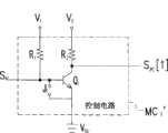
依据本发明的较佳实施例,节电模块包含基板管理控制器(baseboardmanagement controller,BMC)、多个控制电路。各控制电路耦接至基板管理控制器。基板管理控制器向中央处理器请求功耗信息,依据功耗信息产生启动信号至各控制电路。各控制电路依据启动信号,产生电源控制信号。According to a preferred embodiment of the present invention, the power saving module includes a baseboard management controller (BMC) and a plurality of control circuits. Each control circuit is coupled to the baseboard management controller. The baseboard management controller requests power consumption information from the central processing unit, and generates a start signal to each control circuit according to the power consumption information. Each control circuit generates a power control signal according to the start signal.
依据本发明的较佳实施例,前述控制电路包含第一晶体管、第一电阻和第二电阻。其中第一晶体管的基极耦接到基板管理控制器,第一晶体管的集电极耦接到开关,第一晶体管的发射极耦接至第一参考电压。第一电压源经第一电阻,提供上拉(pull high)电压给第一晶体管的基极。第二电压源经第二电阻耦接到第一晶体管的集电极,提供上拉电压给第一晶体管的集电极。依据启动信号,第一晶体管的集电极产生电源控制信号。According to a preferred embodiment of the present invention, the aforementioned control circuit includes a first transistor, a first resistor and a second resistor. The base of the first transistor is coupled to the baseboard management controller, the collector of the first transistor is coupled to the switch, and the emitter of the first transistor is coupled to the first reference voltage. The first voltage source provides a pull-up (pull high) voltage to the base of the first transistor via the first resistor. The second voltage source is coupled to the collector of the first transistor through the second resistor, and provides a pull-up voltage to the collector of the first transistor. According to the enable signal, the collector of the first transistor generates a power control signal.
依据本发明的较佳实施例,上述节电模块更包含短路端子(jumper)。其中,短路端子用于人为控制,使用短路端子耦接于第一晶体管的基极和发射极之间,以控制第一晶体管输出电源控制信号。According to a preferred embodiment of the present invention, the power saving module further includes a jumper. Wherein, the short-circuit terminal is used for manual control, and the short-circuit terminal is coupled between the base and the emitter of the first transistor to control the first transistor to output a power control signal.
依据本发明的较佳实施例,上述基板管理控制器包含检测模块。此检测模块用于向中央处理器请求功耗信息,以致使基板管理控制器依据功耗信息产生启动信号。According to a preferred embodiment of the present invention, the baseboard management controller includes a detection module. The detection module is used to request power consumption information from the central processing unit, so that the baseboard management controller generates a start signal according to the power consumption information.
依据本发明的较佳实施例,其中前述开关包含金属氧化物半导体场效晶体管,以及相位芯片为国际整流器公司(International Rectifier,IR)的IR3505集成电路。金属氧化物半导体场效晶体管用于将漏极与源极分别耦接至IR3505集成电路的第9引脚与第14引脚。金属氧化物半导体场效晶体管根据电源控制信号,用于禁能IR3505集成电路。According to a preferred embodiment of the present invention, the aforementioned switches include metal oxide semiconductor field effect transistors, and the phase chip is an IR3505 integrated circuit of International Rectifier (IR). Mosfets are used to couple the drain and source to
依据本发明的较佳实施例,前述电压调整电路包含第一输出电压阳极引脚、第一输出电压阴极引脚、第一电容器、第一n型金属氧化物半导体场效晶体管、第二n型金属氧化物半导体场效晶体管和第一电感。第一输出电压阳极引脚,为前述直流-直流转换器功率输出的阳极引脚,第一输出电压阴极引脚,为前述直流-直流转换器功率输出的阴极引脚。第一电容器耦接于第一输出电压阳极引脚和第一输出电压阴极引脚中间,用于直流-直流转换器功率输出的稳压效果。第一n型金属氧化物半导体晶体管的漏极耦接到第三电压源,第一n型金属氧化物半导体晶体管的栅极耦接至前述相位芯片IR3505集成电路的第11引脚。第二n型金属氧化物半导体场效晶体管的漏极耦接到第一n型金属氧化物半导体晶体管的源极,第二n型金属氧化物半导体场效晶体管的源极耦接到第一输出电压阴极引脚,第二n型金属氧化物半导体场效晶体管的栅极耦接到IR3505集成电路的第8引脚。第一电感的一端耦接到第一n型金属氧化物半导体晶体管的源极,第一电感的另一端耦接到第一输出电压阳极引脚。IR3505集成电路驱动电压调整电路输出为功率输出其中之一。According to a preferred embodiment of the present invention, the aforementioned voltage adjustment circuit includes a first output voltage anode pin, a first output voltage cathode pin, a first capacitor, a first n-type metal oxide semiconductor field effect transistor, a second n-type metal oxide semiconductor field effect transistor and first inductor. The anode pin of the first output voltage is the anode pin of the power output of the aforementioned DC-DC converter, and the cathode pin of the first output voltage is the cathode pin of the power output of the aforementioned DC-DC converter. The first capacitor is coupled between the anode pin of the first output voltage and the cathode pin of the first output voltage, and is used for the voltage stabilization effect of the power output of the DC-DC converter. The drain of the first n-type metal-oxide-semiconductor transistor is coupled to the third voltage source, and the gate of the first n-type metal-oxide-semiconductor transistor is coupled to the eleventh pin of the aforementioned phase chip IR3505 integrated circuit. The drain of the second nMOSFET is coupled to the source of the first nMOSFET, and the source of the second nMOSFET is coupled to the first output The voltage cathode pin, the gate of the second nMOSFET is coupled to pin 8 of the IR3505 integrated circuit. One end of the first inductor is coupled to the source of the first nMOS transistor, and the other end of the first inductor is coupled to the anode pin of the first output voltage. The output of the IR3505 integrated circuit driving voltage adjustment circuit is one of the power outputs.
依据本发明的较佳实施例,前述节电模块经由芯片组,耦接至中央处理器。依据本发明的较佳实施例,上述节电模块经由低脚位总线(Low Pin Countbus,LPC bus)耦接到芯片组。依据本发明的较佳实施例,上述芯片组,包含北桥芯片和南桥芯片,其中北桥芯片耦接到中央处理器,南桥芯片耦接于北桥芯片和节电模块之间。According to a preferred embodiment of the present invention, the aforementioned power saving module is coupled to the central processing unit via a chipset. According to a preferred embodiment of the present invention, the power saving module is coupled to the chipset via a Low Pin Count bus (LPC bus). According to a preferred embodiment of the present invention, the chip set includes a north bridge chip and a south bridge chip, wherein the north bridge chip is coupled to the CPU, and the south bridge chip is coupled between the north bridge chip and the power-saving module.
现有支持多款中央处理器的计算机平台,使用多相功率转换器来设计中央处理器的电源供应单元。为了在使用不同功率消耗的中央处理器时,增加电源供应单元的转换效率,本发明提出一种计算机的电源管理装置,向中央处理器取得功耗信息,来决定多相功率转换器所使用的相数,以驱动功率输出到中央处理器。借由本发明提出的电源管理装置,可提升电源供应单元的转换效率。Existing computer platforms that support a variety of CPUs use multi-phase power converters to design power supply units for CPUs. In order to increase the conversion efficiency of the power supply unit when using CPUs with different power consumptions, the present invention proposes a computer power management device that obtains power consumption information from the CPU to determine the power used by the multi-phase power converter. Number of phases to drive power output to the CPU. With the power management device proposed by the present invention, the conversion efficiency of the power supply unit can be improved.
上述说明仅是本发明技术方案的概述,为了能够更清楚了解本发明的技术手段,并可依照说明书的内容予以实施,以下以本发明的较佳实施例并配合附图详细说明如后。The above description is only an overview of the technical solutions of the present invention. In order to understand the technical means of the present invention more clearly and implement them according to the contents of the description, the preferred embodiments of the present invention and accompanying drawings are described in detail below.
附图说明Description of drawings
图1为根据本发明所绘示的一种中央处理器的电源管理装置结构图。FIG. 1 is a structural diagram of a power management device for a CPU according to the present invention.
图2是依照本发明较佳实施例所绘示的功率转换器结构图。FIG. 2 is a structural diagram of a power converter according to a preferred embodiment of the present invention.
图3A-图3B是依照本发明较佳实施例所绘示的相位信号传输架构图。3A-3B are structural diagrams of phase signal transmission according to a preferred embodiment of the present invention.
图4依照本发明较佳实施例所绘示的直流-直流转换器结构图。FIG. 4 is a structural diagram of a DC-DC converter according to a preferred embodiment of the present invention.
图5是依照本发明较佳实施例所绘示的节电模块架构图。FIG. 5 is a structural diagram of a power-saving module according to a preferred embodiment of the present invention.
图6A-图6B是依照本发明较佳实施例所绘示的控制电路图。6A-6B are control circuit diagrams according to a preferred embodiment of the present invention.
图7是依照本发明较佳实施例所绘示的开关和相位芯片的电路图。FIG. 7 is a circuit diagram of a switch and a phase chip according to a preferred embodiment of the present invention.
图8是依照本发明较佳实施例所绘示的电压调整电路图。FIG. 8 is a circuit diagram of a voltage adjustment circuit according to a preferred embodiment of the present invention.
图9是依照本发明较佳实施例所绘示的中央处理器功耗信息存取流程图。FIG. 9 is a flow chart of CPU power consumption information access according to a preferred embodiment of the present invention.
主要元件符号说明:Description of main component symbols:
100:电源管理装置 110:中央处理器100: power management device 110: central processing unit
200、200’:功率转换器200, 200': power converter
310:开关 320:相位芯片310: switch 320: phase chip
330:电压调整电路330: Voltage adjustment circuit
400:脉宽调变控制器400: Pulse Width Modulation Controller
500:节电模块 510:基板管理控制器500: Power saving module 510: Baseboard management controller
930:芯片组 931:北桥芯片930: Chipset 931: North Bridge Chip
932:南桥芯片 950:低脚位总线932: South Bridge Chip 950: Low Pin Bus
C1:电容器C1 : Capacitor
CVT1~CVTN:直流-直流转换器CVT1 ~CVTN : DC-DC converter
J1:短路端子J1 : Short circuit terminal
L1:电感L1 : Inductance
MC1~MCN、MC1’:控制电路MC1 ~MCN , MC1 ': control circuit
P1~PN:功率输出P1 ~PN : power output
Q1:晶体管Q1 : Transistor
Q2:金属氧化物半导体场效晶体管Q2 : Metal Oxide Semiconductor Field Effect Transistor
Q3、Q4:n型金属氧化物半导体场效晶体管Q3 , Q4 : n-type metal-oxide-semiconductor field-effect transistors
R1、R2:电阻R1 , R2 : Resistance
SA1~SAN:启动信号SA1 ~SAN : start signal
SDR:驱动信号SDR : drive signal
SPC[N..1]:电源控制信号SPC [N..1]: Power supply control signal
SPC[1]~SPC[N]:电源控制信号SPC [1]~SPC [N]: Power control signal
SP、SP0、SP1~SPN:相位信号SP , SP0 , SP1 ~ SPN : phase signal
V1、V2、V3、V4:电压源V1 , V2 , V3 , V4 : Voltage sources
VOUT+:输出电压阳极引脚VOUT+ : output voltage anode pin
VOUT-:输出电压阴极引脚VOUT- : Output voltage cathode pin
具体实施方式Detailed ways
以下结合附图及较佳实施例,对依据本发明提出一种计算机的电源管理装置,其特征及其功效详细说明如后。A power management device for a computer according to the present invention is described below in conjunction with the accompanying drawings and preferred embodiments, and its features and functions are described in detail below.
本发明所属领域的通常技术人员应知现有计算机的新一代中央处理器,如英特尔(Intel)的Pentium 4,依循英特尔的新一代电源管理标准-降压式电压调整器(voltage regulator down,VRD)规范,来设计中央处理器的电源供应单元。降压式电压调整器使用多相降压转换器(multi-phases bulk converter),使用多相功率输出,提供中央处理器所需功率消耗。此处所提中央处理器不限定于Pentium4,可以是任一款支持降压式电压调整器规范的中央处理器。图1为根据本发明所绘示的一种中央处理器的电源管理装置结构图。由于计算机平台能支持的中央处理器不限定于一种,而多款中央处理器的消耗功率也不尽相同。Those skilled in the art of the present invention should know that the new-generation central processing unit of existing computers, such as the Pentium 4 of Intel (Intel), follows Intel's new-generation power management standard-step-down voltage regulator (voltage regulator down, VRD ) specification to design the power supply unit of the central processing unit. The buck voltage regulator uses a multi-phases bulk converter, which uses multi-phase power output to provide the power consumption required by the CPU. The CPU mentioned here is not limited to Pentium4, and can be any CPU that supports the step-down voltage regulator specification. FIG. 1 is a structural diagram of a power management device for a CPU according to the present invention. Since the CPU supported by the computer platform is not limited to one type, the power consumption of various CPUs is also different.
本发明所提出电源管理装置100,由节电模块500向中央处理器110请求功耗信息,而依据中央处理器110所响应的功耗信息,输出电源控制信号SPC[N..1]到功率转换器200。电源控制信号SPC[N..1]具有N个信号,分别控制功率转换器200中的各相直流-直流转换器,此直流-直流转换器提供多个功率输出分别为P1~PN。功率转换器200依据电源控制信号SPC[N..1]决定致能所述功率输出P1~PN的数量。也就是说,当电源控制信号SPC[N..1]禁能功率转换器200中的任一直流-直流转换器时,因应电源控制信号SPC[N..1],功率转换器200调整总功率输出,提供中央处理器110所需用于运作的功耗。英特尔的另一电源管理规范-企业电压调整器模块(Enterprise VRD,EVRD)规范,与降压式电压调整器规范的差异在于企业电压调整器模块规范支持多处理器的计算机平台;依据本发明可视为多个中央处理器-电源管理装置组,故在此不再赘述。In the
如前所述,功率转换器200用于决定输出功率。图2是依照本发明较佳实施例所绘示的功率转换器结构图。功率转换器200包含脉宽调变控制器400和N个直流-直流转换器CVT1~CVTN。脉宽调变控制器400产生相位信号SP;本发明所属领域的通常技术人员应知此相位信号SP是参考中央处理器110的电压辨识(voltage ID,VID)决定,此一过程不再赘述。脉宽调变控制器400输出相位信号SP至直流-直流转换器CVT1~CVTN,各直流-直流转换器CVT1~CVTN产生功率输出到中央处理器110。以下将用图3A-图3B对于驱动直流-直流转换器CVT1~CVTN的过程,做进一步描述。As mentioned above, the
图3A-图3B是依照本发明较佳实施例所绘示的相位信号传输架构图。节电模块500产生电源控制信号SPC[N..1],分别用于禁能直流-直流转换器CVT1~CVTN。当任一直流-直流转换器被致能时,此被致能的直流-直流转换器依据相位信号产生功率输出;当任一直流-直流转换器被禁能时,此被禁能的直流-直流转换器即关闭功率输出。图3A中所示为相位信号传递的方式依据国际整流器公司的XPhase3TM架构。其中直流-直流转换器CVT1~CVTN串联耦接至所述脉宽调变控制器400,脉宽调变控制器400输出相位信号SP1至直流-直流转换器CVT1。当直流-直流转换器CVT1被致能时,直流-直流转换器CVT1产生功率输出P1至中央处理器110。同时直流-直流转换器CVT1将相位信号SP1移位(shift)输出相位信号SP2到直流-直流转换器CVT2,以此类推。最终相位信号SPN经由直流-直流转换器CVTN移位输出相位信号SP0反馈给脉宽调变控制器400。此XPhase3TM架构的特性在于直流-直流转换器CVT1~CVTN以串联型态耦接以接收相位信号,优点是利用相位信号移位的方式,可节省产生相位信号的引脚数量。3A-3B are structural diagrams of phase signal transmission according to a preferred embodiment of the present invention. The
以下将另举一实施例,说明相位信号用不同传递方式的应用。图3B与图3A的差异处,在于相位信号的传递方式。请参照图3B,其中直流-直流转换器CVT1~CVTN并联耦接至所述脉宽调变控制器400。节电模块500产生电源控制信号SPC[N..1],分别用于禁能直流-直流转换器CVT1~CVTN。当直流-直流转换器被致能时,即依据相位信号产生功率输出。脉宽调变控制器400依序移位产生相位信号SP1~SPN,个别输出至直流-直流转换器CVT1~CVTN;在此仅以直流-直流转换器CVT1作为说明。直流-直流转换器CVT1默认为致能状态,直流-直流转换器CVT1依据脉宽调变控制器400的相位信号SP1,产生功率输出P1至中央处理器110。当相位信号SP1产生后,脉宽调变控制器400移位产生相位信号SP2以输出至直流-直流转换器CVT2。其它直流-直流转换器以此类推。Another embodiment will be given below to illustrate the application of phase signals in different transmission modes. The difference between FIG. 3B and FIG. 3A lies in the transmission mode of the phase signal. Please refer to FIG. 3B , wherein the DC-DC converters CVT1 -CVTN are coupled in parallel to the
以下针对直流-直流转换器的架构,仅以直流-直流转换器CVT1作为说明例。图4依照本发明较佳实施例所绘示的直流-直流转换器CVT1结构图,包含电压调整电路330、相位芯片320和开关310。在此所述开关310可以是晶体管、其它电路等。开关310耦接到相位芯片320的致能端口EN。相位芯片320依据脉宽调变控制器400输出的相位信号SP1,驱动电压调整电路330产生功率输出P1。当节电模块500产生电源控制信号SPC[1]输出至开关310时,开关310禁能相位芯片320。For the structure of the DC-DC converter, the DC-DC converter CVT1 is used as an example for illustration. FIG. 4 is a structural diagram of a DC-DC converter CVT1 according to a preferred embodiment of the present invention, including a
图5是依照本发明较佳实施例所绘示的节电模块架构图。节电模块500包含基板管理控制器510和N个控制电路MC1~MCN。基板管理控制器510包含检测模块,请参照图1,基板管理控制器510的检测模块向中央处理器110请求功耗信息,而后基板管理控制器510依据中央处理器110所响应的功耗信息来决定功率转换器200产生功率输出的相数。本发明所属领域的通常技术人员可以任何方式实现基板管理控制器510的检测模块,使得所述检测模块可以向中央处理器110取得功耗信息。例如,检测模块的实现方式可以如同基本输入输出系统(BIOS)在计算机的开机过程中对中央处理器进行检测。亦即,本发明所属领域的通常技术人员可依据本实施例的说明,透过更改基板管理控制器510的韧体(firmware)来达成检测模块的功效。FIG. 5 is a structural diagram of a power-saving module according to a preferred embodiment of the present invention. The
在此仅以控制电路MC1代表说明之,本发明所属领域的通常技术人员可依据本实施例的说明,类推至其它的控制电路。基板管理控制器510耦接至控制电路MC1,控制电路MC1耦接至功率转换器200的直流-直流转换器CVT1。当基板管理控制器510产生启动信号SA1时,控制电路MC1依据启动信号SA1产生电源控制信号SPC[1]。控制电路MC1输出电源控制信号SPC[1]至直流-直流转换器CVT1,用以禁能直流-直流转换器CVT1。Here, only the control circuit MC1 is used for illustration, and those skilled in the art of the present invention can deduce other control circuits according to the description of this embodiment. The
图6A-图6B是依照本发明较佳实施例所绘示的控制电路图,在此仅以控制电路MC1说明。控制电路MC1耦接于基板管理控制器510和功率转换器200之间,依据基板管理控制器510输出的启动信号SA1,控制电路MC1产生电源控制信号SPC[1]。图6A并未绘出控制电路MC1的完整电路,仅择要地绘示晶体管Q1、电阻R1和电阻R2。其中晶体管Q1可以是PNP、NPN、其它晶体管(依据所使用实施例修改控制电路)。电阻R1耦接于电压源V1和晶体管Q1的基极之间,提供上拉电压给晶体管Q1的基极(晶体管Q1的基极默认为高电平)。晶体管Q1的基极耦接到底板控制管理器510,用以接收底板控制管理器510产生的启动信号SA1。电阻R2耦接于电压源V2和晶体管Q1的集电极之间,提供上拉电压给晶体管Q1的集电极(晶体管Q1的集电极默认为高电平)。晶体管Q1的集电极耦接至功率转换器200的直流-直流转换器CVT1,用以致能直流-直流转换器CVT1。晶体管Q1的发射极耦接到参考电压VSS1。当晶体管Q1的基极为高电平(默认值),此时晶体管Q1导通,晶体管Q1的集电极电压电平参考至参考电压VSS;晶体管Q1的集电极电压维持低电平状态,输出至直流-直流转换器CVT1。当基板管理控制器510产生启动信号SA1(低电平)时,晶体管Q1截止,晶体管Q1的集电极电压电平参考至上拉电压,此时晶体管Q1的集电极产生电源控制信号SPC[1](高电平),输出至直流-直流转换器CVT1。6A-6B are control circuit diagrams according to a preferred embodiment of the present invention, and here only the control circuit MC1 is used for illustration. The control circuit MC1 is coupled between the
上述实施例是以基板管理控制器510来控制功率转换器200内部多个直流-直流转换器CVT1~CVTN的致能状态。以下将另举一实施例,说明以人为控制的方式,来控制功率转换器200内部多个直流-直流转换器CVT1~CVTN的致能状态。图6B是依照本发明另一较佳实施例所绘示的控制电路MC1’架构图,在此仅以控制电路MC1说明。此处并未绘出控制电路MC1的完整电路,仅择要地绘示晶体管Q1、电阻R1和电阻R2。请参照图6B,在控制电路MC1’中设置一个短路端子J1,耦接于在晶体管Q1的基极和发射极之间。如果已经知道中央处理器110的功耗信息,使用此短路端子J1将晶体管Q1的基极和发射极短路(short),使晶体管Q1的基极电压电平参考至参考电压VSS1(低电平)。此举等同于基板管理控制器510发出启动信号SA1(低电平),使晶体管Q1截止,晶体管Q1的集电极电压电平参考至上拉电压。此时晶体管Q1的集电极产生电源控制信号SPC[1](高电平),输出至直流-直流转换器CVT1。In the above embodiment, the
依据前述图3A-图3B所述相位信号的传递方式,相位芯片320实际规格与硬件规划有关。图7是依照本发明较佳实施例所绘示开关和相位芯片的电路图,此处并未绘出开关310和相位芯片320的完整电路,仅择要地绘示金属氧化物半导体场效晶体管Q2、IR3505集成电路。其中开关310包含金属氧化物半导体场效晶体管Q2,相位芯片320为国际整流器公司的IR3505集成电路;本实施例虽以金属氧化物半导体场效晶体管Q2作为开关310的实施代表,但所属技术领域的通常技术人员亦可以依据本实施例的说明,而类推至pMOS场效晶体管、nMOS场效晶体管、具有开关功能的电子组件、其它电路。依据IR3505集成电路的规格说明书,当IR3505集成电路第14引脚的输入电压,被上拉到和第9引脚的电压相同时,IR3505集成电路将进入调试模式(debug mode),等同于禁能IR3505集成电路。According to the transmission mode of the phase signal described above in FIGS. 3A-3B , the actual specification of the
在此仅以控制电路MC1、开关310和相位芯片320的耦接关系说明。控制电路MC1耦接至直流-直流转换器CVT1,直流-直流转换器CVT1包含开关310和相位芯片320。金属氧化物半导体场效晶体管Q2的漏极与源极分别耦接至IR3505集成电路的第9引脚与第14引脚。电压源V4耦接至IR3505集成电路的第9引脚。金属氧化物半导体场效晶体管Q2的栅极耦接至节电模块500的控制电路MC1,参照前文,金属氧化物半导体场效晶体管Q2的栅极电压电平默认为低电平;因此,金属氧化物半导体场效晶体管Q2截止,IR3505集成电路的第9引脚的电压不同于第14引脚的电压。Here, only the coupling relationship of the control circuit MC1 , the
要关闭直流-直流转换器CVT1,可利用基板管理控制器510产生启动信号SA1(低电平),使控制电路MC1产生电源控制信号SPC[1](高电平)输出至金属氧化物半导体场效晶体管Q2的栅极,此时金属氧化物半导体场效晶体管Q2导通,IR3505集成电路的第9引脚和第14引脚之间形成短路,禁能IR3505集成电路。To turn off the DC-DC converter CVT1 , the
在本实施例中,直流-直流转换器包含电压转换电路和相位芯片,此处举直流-直流转换器CVT1代表说明。请参照图8,电压转换电路330耦接于相位芯片320和中央处理器110之间,相位芯片320驱动电压转换电路330产生功率输出至中央处理器110。图8是依照本发明较佳实施例所绘示电压调整电路图,此处并未绘出电压调整电路330的完整电路图,仅择要地绘示输出电压阳极引脚VOUT+、输出电压阴极引脚VOUT-、电容器C1、n型金属氧化物半导体场效晶体管Q3、n型金属氧化物半导体场效晶体管Q4和电感L1。输出电压阳极引脚VOUT+为直流-直流转换器CVT1的功率输出阳极引脚,输出电压阴极引脚VOUT-为前述直流-直流转换器CVT1的功率输出阴极引脚。电容器C1耦接于输出电压阳极引脚VOUT+和输出电压阴极引脚VOUT-中间,用于直流-直流转换器CVT1所产生功率输出的稳压效果。n型金属氧化物半导体晶体管Q3的漏极耦接到电压源V3。前述驱动信号SDR由相位芯片IR3505集成电路的第8引脚和第11引脚传递。In this embodiment, the DC-DC converter includes a voltage conversion circuit and a phase chip, and the DC-DC converter CVT1 is used here as a representative for illustration. Referring to FIG. 8 , the
n型金属氧化物半导体场效晶体管Q3的栅极耦接至IR3505集成电路的第11引脚。n型金属氧化物半导体场效晶体管Q4的漏极耦接到n型金属氧化物半导体场效晶体管Q3的源极,n型金属氧化物半导体场效晶体管Q4的源极耦接到输出电压阴极引脚VOUT-,n型金属氧化物半导体场效晶体管Q4的栅极耦接到IR3505集成电路的第8引脚。电感L1的一端耦接到n型金属氧化物半导体场效晶体管Q3的源极。电感L1的另一端耦接到输出电压阳极引脚VOUT+。当IR3505集成电路的第11引脚输出高电平而IR3505集成电路的第8引脚输出低电平时,n型金属氧化物半导体场效晶体管Q3的源极和漏极导通,n型金属氧化物半导体场效晶体管Q4的源极和漏极断开,电压源V3储存电能电感L1。当IR3505集成电路的第11引脚输出低电平而IR3505集成电路的第8引脚输出高电平时,n型金属氧化物半导体场效晶体管Q3的源极和漏极断开,n型金属氧化物半导体场效晶体管Q4的源极和漏极导通,此时电感L1释放电能,透过电容器C1稳压输出为功率输出P1。The gate of the nMOSFETQ3 is coupled to the eleventh pin of the IR3505 integrated circuit. The drain of nMOSFETQ4 is coupled to the source of nMOSFETQ3 , and the source of nMOSFETQ4 is coupled to the output The voltage cathode pin VOUT- , the gate of the nMOSFETQ4 is coupled to pin 8 of the IR3505 integrated circuit. One end of the inductorL1 is coupled to the source of the nMOSFETQ3 . The other end of the inductor L1 is coupled to the output voltage anode pin VOUT+ . When the 11th pin of the IR3505 integrated circuit outputs a high level and the 8th pin of the IR3505 integrated circuit outputs a low level, the source and drain of the n-type MOSFETQ3 are turned on, and the n-type metal The source and drain of the oxide semiconductor field effect transistor Q4 are disconnected, and the voltage source V3 stores electric energy in the inductor L1 . When the 11th pin of the IR3505 integrated circuit outputs a low level and the 8th pin of the IR3505 integrated circuit outputs a high level, the source and drain of the n-type MOSFETQ3 are disconnected, and the n-type metal The source and drain of the oxide semiconductor field effect transistor Q4 are turned on, and at this moment, the inductor L1 releases electric energy, and the voltage output through the capacitor C1 is stabilized and output as a power output P1 .
在本实施例中,节电模块500向中央处理器110请求功耗信息。图9是依照本发明较佳实施例所绘示中央处理器功耗信息的存取流程图。节电模块500的基板管理控制器510,耦接至低脚位总线950;芯片组930耦接至低脚位总线950和中央处理器110。基板管理控制器510经由低脚位总线950向芯片组930发出中央处理器110功耗信息的请求命令。芯片组930包含南桥芯片932和北桥芯片931,南桥芯片932耦接至北桥芯片931和低脚位总线950,北桥芯片931耦接至中央处理器110。本发明所属领域的通常技术人员应知计算机的内部芯片组和总线架构,故不在此赘述详细过程。前述功耗信息的请求命令经由低脚位总线950、南桥芯片932、北桥芯片931转送至中央处理器110。中央处理器110接收请求命令后,响应功耗信息经北桥芯片931、南桥芯片932、低脚位总线950转送至基板管理控制器510,作为产生启动信号SA1~SAN的依据,进而调整功率产生器200的功率输出,因应中央处理器110的功率消耗以关闭多余的直流-直流转换器,提升电源供应单元的转换效率。In this embodiment, the
以上所述,仅是本发明的较佳实施例而已,并非对本发明作任何形式上的限制,虽然本发明已以较佳实施例揭露如上,然而并非用以限定本发明,任何熟悉本专业的技术人员,在不脱离本发明技术方案范围内,当可利用上述揭示的结构及技术内容作出些许的更动或修饰为等同变化的等效实施例,但是凡是未脱离本发明技术方案的内容,依据本发明的技术实质对以上实施例所作的任何简单修改、等同变化与修饰,均仍属于本发明技术方案的范围内。The above description is only a preferred embodiment of the present invention, and does not limit the present invention in any form. Although the present invention has been disclosed as above with preferred embodiments, it is not intended to limit the present invention. Anyone familiar with this field Those skilled in the art, without departing from the scope of the technical solution of the present invention, may use the structure and technical content disclosed above to make some changes or modifications to equivalent embodiments with equivalent changes, but any content that does not depart from the technical solution of the present invention, Any simple modifications, equivalent changes and modifications made to the above embodiments according to the technical essence of the present invention still fall within the scope of the technical solutions of the present invention.
Claims (11)
Priority Applications (1)
| Application Number | Priority Date | Filing Date | Title |
|---|---|---|---|
| CN2008101757070ACN101727170B (en) | 2008-10-31 | 2008-10-31 | CPU power management device |
Applications Claiming Priority (1)
| Application Number | Priority Date | Filing Date | Title |
|---|---|---|---|
| CN2008101757070ACN101727170B (en) | 2008-10-31 | 2008-10-31 | CPU power management device |
Publications (2)
| Publication Number | Publication Date |
|---|---|
| CN101727170A CN101727170A (en) | 2010-06-09 |
| CN101727170Btrue CN101727170B (en) | 2012-05-23 |
Family
ID=42448152
Family Applications (1)
| Application Number | Title | Priority Date | Filing Date |
|---|---|---|---|
| CN2008101757070AExpired - Fee RelatedCN101727170B (en) | 2008-10-31 | 2008-10-31 | CPU power management device |
Country Status (1)
| Country | Link |
|---|---|
| CN (1) | CN101727170B (en) |
Families Citing this family (6)
| Publication number | Priority date | Publication date | Assignee | Title |
|---|---|---|---|---|
| US9658666B1 (en)* | 2015-12-18 | 2017-05-23 | Intel Corporation | Dynamic capacitor modulated voltage regulator |
| US10209726B2 (en)* | 2016-06-10 | 2019-02-19 | Microsoft Technology Licensing, Llc | Secure input voltage adjustment in processing devices |
| CN111324166B (en)* | 2018-12-14 | 2021-09-03 | 技嘉科技股份有限公司 | Power regulator and power regulation method |
| FR3101933B1 (en)* | 2019-10-15 | 2021-10-01 | Valeo Vision | LIGHTING SYSTEM INCLUDING A MULTI-PHASE INTERLACED POWER CONVERTER |
| US11071206B2 (en)* | 2019-10-17 | 2021-07-20 | Infineon Technologies Austria Ag | Electronic system and processor substrate having an embedded power device module |
| US12093113B2 (en)* | 2022-07-25 | 2024-09-17 | Shaoxing Yuanfang Semiconductor Co., Ltd. | Communicating a desired power state to a power stage from a phase controller in a power supply |
Citations (5)
| Publication number | Priority date | Publication date | Assignee | Title |
|---|---|---|---|---|
| US5659789A (en)* | 1995-12-15 | 1997-08-19 | Compaq Computer Corporation | Stopclock toggle system for powering two CPUs from a regulator only sized for one CPU |
| CN1396509A (en)* | 2001-07-05 | 2003-02-12 | Lg电子株式会社 | Power supply of central processing unit |
| CN1443319A (en)* | 2000-07-24 | 2003-09-17 | 先进微装置公司 | Method and apparatus to provide deterministic power-on voltage in system having processor-controlled voltage level |
| US6691235B1 (en)* | 2000-07-27 | 2004-02-10 | International Business Machines Corporation | Automatic voltage regulation for processors having different voltage requirements and unified or split voltage planes |
| CN1909347A (en)* | 2006-08-11 | 2007-02-07 | 友达光电股份有限公司 | DC to DC conversion circuit with adjustable output voltage |
- 2008
- 2008-10-31CNCN2008101757070Apatent/CN101727170B/ennot_activeExpired - Fee Related
Patent Citations (5)
| Publication number | Priority date | Publication date | Assignee | Title |
|---|---|---|---|---|
| US5659789A (en)* | 1995-12-15 | 1997-08-19 | Compaq Computer Corporation | Stopclock toggle system for powering two CPUs from a regulator only sized for one CPU |
| CN1443319A (en)* | 2000-07-24 | 2003-09-17 | 先进微装置公司 | Method and apparatus to provide deterministic power-on voltage in system having processor-controlled voltage level |
| US6691235B1 (en)* | 2000-07-27 | 2004-02-10 | International Business Machines Corporation | Automatic voltage regulation for processors having different voltage requirements and unified or split voltage planes |
| CN1396509A (en)* | 2001-07-05 | 2003-02-12 | Lg电子株式会社 | Power supply of central processing unit |
| CN1909347A (en)* | 2006-08-11 | 2007-02-07 | 友达光电股份有限公司 | DC to DC conversion circuit with adjustable output voltage |
Also Published As
| Publication number | Publication date |
|---|---|
| CN101727170A (en) | 2010-06-09 |
Similar Documents
| Publication | Publication Date | Title |
|---|---|---|
| US9337735B2 (en) | DC/DC converter within a portable computer | |
| CN110649694B (en) | NCSI network card power supply system | |
| CN103930848B (en) | Power Management for Electronic Devices | |
| CN110323736A (en) | Power supply switch circuit and electronic equipment | |
| CN101727170B (en) | CPU power management device | |
| US11205962B2 (en) | Real-time switching period estimation apparatus and method | |
| TWI375872B (en) | Multi-phase voltage regulator module and method controlling the same | |
| CN107819340A (en) | AC-battery power source buck charger | |
| EP2153514A2 (en) | Computer system power source with improved light-load efficiency | |
| CN100565428C (en) | Computing machine and control method thereof | |
| CN104682692A (en) | Power management unit | |
| WO2017176341A1 (en) | Dynamic voltage regulator sensing and reference voltage setting techniques for multiple gated loads | |
| CN103869852B (en) | Voltage regulators and electronics | |
| US12113442B2 (en) | Stacked buck converter with inductor switching node pre-charge and conduction modulation control | |
| CN117097165A (en) | Driving scheme for secondary controlled Active Clamp Flyback (ACF) mode | |
| US20090199021A1 (en) | Power management module for central processing unit | |
| CN101470512A (en) | Power supply management module of central processing unit | |
| TWI877221B (en) | Power supply apparatus and electronic system | |
| TW200412004A (en) | Adjustable power supply device with multiple input voltage levels | |
| US20090225618A1 (en) | Power management module for memory module | |
| TWI465917B (en) | Bridging device and energy saving method thereof | |
| CN105048810B (en) | A kind of adaptive voltage scaling circuit for power inverter | |
| CN101470505A (en) | Power management module of memory module | |
| Zhang et al. | Adaptive pseudo-continuous conduction mode operation schemes and circuit designs for single-inductor multiple-output switching converters | |
| US10216253B2 (en) | Universal serial bus hub and control method thereof |
Legal Events
| Date | Code | Title | Description |
|---|---|---|---|
| C06 | Publication | ||
| PB01 | Publication | ||
| C10 | Entry into substantive examination | ||
| SE01 | Entry into force of request for substantive examination | ||
| C14 | Grant of patent or utility model | ||
| GR01 | Patent grant | ||
| TR01 | Transfer of patent right | ||
| TR01 | Transfer of patent right | Effective date of registration:20170818 Address after:Room 8, building 805, sunshine times, Fenghuang Road, Fenghuang County, Shangrao, Jiangxi, Shangrao Co-patentee after:Zhang Kaijun Patentee after:Jiangxi union Speed Technology Co.,Ltd. Address before:Qingnian Road Taiwan Wanhua District of Taipei city China No. 184 3 2 floor Patentee before:Fucheng International Machinery Co.,Ltd. Effective date of registration:20170818 Address after:Qingnian Road Taiwan Wanhua District of Taipei city China No. 184 3 2 floor Patentee after:Fucheng International Machinery Co.,Ltd. Address before:Taipei City, Taiwan Chinese Shilin District Hougang Street No. 66 Patentee before:Yingda Co.,Ltd. | |
| CF01 | Termination of patent right due to non-payment of annual fee | ||
| CF01 | Termination of patent right due to non-payment of annual fee | Granted publication date:20120523 Termination date:20171031 |