CN101726954B - Pixel structure - Google Patents
Pixel structureDownload PDFInfo
- Publication number
- CN101726954B CN101726954BCN2009102619138ACN200910261913ACN101726954BCN 101726954 BCN101726954 BCN 101726954BCN 2009102619138 ACN2009102619138 ACN 2009102619138ACN 200910261913 ACN200910261913 ACN 200910261913ACN 101726954 BCN101726954 BCN 101726954B
- Authority
- CN
- China
- Prior art keywords
- pixel electrode
- data line
- pixel
- electrode
- active component
- Prior art date
- Legal status (The legal status is an assumption and is not a legal conclusion. Google has not performed a legal analysis and makes no representation as to the accuracy of the status listed.)
- Active
Links
- 239000000758substrateSubstances0.000claimsabstractdescription37
- 239000003990capacitorSubstances0.000claimsdescription45
- 238000000926separation methodMethods0.000claimsdescription3
- 239000004973liquid crystal related substanceSubstances0.000description15
- 238000010586diagramMethods0.000description13
- 230000000694effectsEffects0.000description10
- 239000010408filmSubstances0.000description9
- 238000005516engineering processMethods0.000description7
- 239000011159matrix materialSubstances0.000description4
- 238000000034methodMethods0.000description4
- 239000010409thin filmSubstances0.000description2
- 239000000463materialSubstances0.000description1
- 238000012986modificationMethods0.000description1
- 230000004048modificationEffects0.000description1
- 230000002093peripheral effectEffects0.000description1
Images


Landscapes
- Liquid Crystal (AREA)
Abstract
Translated fromChinese
Description
Translated fromChinese技术领域technical field
本发明是有关于一种像素结构,且特别是有关于一种可提升显示质量的像素结构。The present invention relates to a pixel structure, and in particular to a pixel structure capable of improving display quality.
背景技术Background technique
市场对于液晶显示面板的性能要求是朝向高对比(high contrast ratio)、无灰阶反转(no gray scale inversion)、色偏小(little color shift)、亮度高(highluminance)、高色彩丰富度、高色彩饱和度、快速反应与广视角等特性。目前,能够达成广视角要求的技术有扭转向列型(twist nematic,TN)液晶加上广视角膜(wide viewing film)、共平面切换型(in-plane switching,IPS)液晶显示面板、边际场切换型(fringe field switching)液晶显示面板、多域垂直配向型(multi-domainvertically alignment,MVA)液晶显示面板等方式。The performance requirements of the market for LCD panels are high contrast ratio, no gray scale inversion, little color shift, high luminance, high color richness, Features such as high color saturation, fast response and wide viewing angle. At present, the technologies that can meet the requirement of wide viewing angle include twist nematic (TN) liquid crystal plus wide viewing film (wide viewing film), in-plane switching (IPS) liquid crystal display panel, fringe field Switching (fringe field switching) liquid crystal display panels, multi-domain vertical alignment (multi-domain vertically aligned, MVA) liquid crystal display panels, etc.
已知的多域垂直配向式液晶显示面板是利用配向结构(alignment structure)的配置以令不同区域内的液晶分子以不同角度倾倒,而达到广视角的功效。配向结构包括有配向凸块(alignment protrusion)以及设置在电极上的配向狭缝(alignment slit)。然而,配向凸块与配向狭缝周边液晶分子的倾倒方向往往不明确(disclination),而造成漏光或产生黑纹现象的情形,进一步使得液晶显示面板的显示对比降低。若为了遮蔽漏光或黑纹现象的情形而配置对应于配向凸块或配向狭缝的遮光层,又会使显示开口率受到限制。The known multi-domain vertical alignment liquid crystal display panel utilizes the configuration of the alignment structure to make the liquid crystal molecules in different regions tilt at different angles, so as to achieve the effect of wide viewing angle. The alignment structure includes alignment protrusions and alignment slits arranged on the electrodes. However, the disclination of the liquid crystal molecules around the alignment bumps and the alignment slits is often unclear, resulting in light leakage or black streaks, which further reduces the display contrast of the liquid crystal display panel. If a light-shielding layer corresponding to the alignment bumps or alignment slits is configured to shield light leakage or black stripes, the display aperture ratio will be limited.
因此,如何在像素结构的广视角需求以及开口率之间取得平衡,实为目前提升像素结构的显示质量亟待克服的课题之一。Therefore, how to strike a balance between the wide viewing angle requirement of the pixel structure and the aperture ratio is actually one of the problems to be solved urgently to improve the display quality of the pixel structure.
发明内容Contents of the invention
本发明提供一种像素结构,其具有高开口率。The invention provides a pixel structure with high aperture ratio.
本发明提供一种像素结构,其可降低显示时的不连续现象,获得良好的显示质量。The invention provides a pixel structure, which can reduce the discontinuous phenomenon during display and obtain good display quality.
本发明提出一种像素结构,其包括基板、扫描线、第一数据线以及第一像素单元。扫描线以及第一数据线配置在基板上。第一像素单元包括第一有源元件以及第一像素电极。第一有源元件与扫描线以及第一数据线电性连接。第一像素电极与第一有源元件电性连接,第一像素电极具有一大体平行扫描线的条状图案以及与条状图案电性连接的多个分支,条状图案的一侧与延伸在扫描线的分支连接,而条状图案的另一侧与扫描线部分重叠,其中条状图案与扫描线的重叠宽度为条状图案的宽度的40%~90%。The present invention provides a pixel structure, which includes a substrate, a scan line, a first data line and a first pixel unit. The scanning lines and the first data lines are arranged on the substrate. The first pixel unit includes a first active element and a first pixel electrode. The first active element is electrically connected to the scan line and the first data line. The first pixel electrode is electrically connected to the first active element, the first pixel electrode has a strip pattern substantially parallel to the scanning line and a plurality of branches electrically connected to the strip pattern, one side of the strip pattern is connected to the The branches of the scanning lines are connected, and the other side of the strip pattern partially overlaps with the scanning line, wherein the overlapping width of the strip pattern and the scanning line is 40%-90% of the width of the strip pattern.
在本发明的一实施例中,上述的分支与第一数据线例如在基板上的投影彼此分离,且第一像素电极与第一数据线具有一间距。In an embodiment of the present invention, the above branch and the projection of the first data line on the substrate, for example, are separated from each other, and there is a distance between the first pixel electrode and the first data line.
在本发明的一实施例中,上述的第一像素电极更具有一主干部以及一支部,主干部平行于第一数据线,支部平行于扫描线,主干部与支部将第一像素单元划分为四个领域,分支自主干部以及支部分的交叉处往周围延伸,其中每一领域中的分支彼此大体平行。In an embodiment of the present invention, the above-mentioned first pixel electrode further has a main part and a branch part, the main part is parallel to the first data line, and the branch part is parallel to the scanning line, and the main part and the branch part divide the first pixel unit into The four domains, the branch main body and the intersection of the branch part extend around, and the branches in each domain are roughly parallel to each other.
在本发明的一实施例中,上述的第一像素单元可更包括储存电容结构,储存电容结构包括下电容电极以及上电容电极,其中上电容电极位在下电容电极上方,上电容电极与第一像素电极为同一膜层,主干部与上电容电极分离,且上电容电极通过邻近数据线的周边的其中的一分支而与第一像素电极连接。In an embodiment of the present invention, the above-mentioned first pixel unit may further include a storage capacitor structure, and the storage capacitor structure includes a lower capacitor electrode and an upper capacitor electrode, wherein the upper capacitor electrode is located above the lower capacitor electrode, and the upper capacitor electrode is connected to the first capacitor electrode. The pixel electrode is of the same film layer, the main part is separated from the upper capacitor electrode, and the upper capacitor electrode is connected to the first pixel electrode through a branch adjacent to the periphery of the data line.
在本发明的一实施例中,上述的像素结构可更包括一彩色滤光层,位于第一有源元件与第一像素电极之间,彩色滤光层具有一个开口,大体位于第一像素电极的主干部与支部的交叉处第一像素电极经由开口与第一有源元件电性连接。此时,第一像素单元可更包括一接触图案,位于主干部与支部的交叉处,并与第一有源元件的一漏极连接,而第一像素电极经由开口与接触图案连接,且第一像素电极例如是以全领域的型态覆盖接触图案。或者,部分分支与接触图案之间例如为至少部分重叠。In an embodiment of the present invention, the above-mentioned pixel structure may further include a color filter layer located between the first active element and the first pixel electrode, the color filter layer has an opening generally located on the first pixel electrode The first pixel electrode is electrically connected to the first active element through the opening at the intersection of the trunk portion and the branch portion. At this time, the first pixel unit may further include a contact pattern, located at the intersection of the trunk portion and the branch portion, and connected to a drain of the first active element, and the first pixel electrode is connected to the contact pattern through the opening, and the second pixel electrode is connected to the contact pattern through the opening. A pixel electrode, for example, covers the contact pattern in the whole area. Or, for example, at least a partial overlap between some branches and the contact pattern.
在本发明的一实施例中,上述的像素结构可更包括第二像素单元以及第二数据线,第二像素单元包括第二有源元件以及第二像素电极。第二有源元件与扫描线以及第二数据线电性连接。第二像素电极与第二有源元件电性连接,第二像素电极具有多个分支,且分支延伸至第一数据线与第二数据线上方并跨越数据线。In an embodiment of the present invention, the aforementioned pixel structure may further include a second pixel unit and a second data line, and the second pixel unit includes a second active element and a second pixel electrode. The second active element is electrically connected with the scan line and the second data line. The second pixel electrode is electrically connected to the second active element, the second pixel electrode has a plurality of branches, and the branches extend above the first data line and the second data line and cross the data line.
在本发明的一实施例中,上述的第一像素单元与第二像素单元例如位于第一数据线与第二数据线之间。In an embodiment of the present invention, the above-mentioned first pixel unit and second pixel unit are, for example, located between the first data line and the second data line.
在本发明的一实施例中,上述的第二像素电极更具有一大体平行扫描线的条状图案,第二像素电极的条状图案的一侧与延伸在扫描线的第二像素电极的分支连接,而第二像素电极的条状图案的另一侧与扫描线部分重叠。具体来说,上述的第二像素电极的条状图案与扫描线的重叠宽度为第二像素电极的条状图案的宽度的40%~90%。In an embodiment of the present invention, the above-mentioned second pixel electrode further has a striped pattern substantially parallel to the scanning line, one side of the striped pattern of the second pixel electrode is connected to the branch of the second pixel electrode extending on the scanning line connected, and the other side of the stripe pattern of the second pixel electrode partially overlaps with the scan line. Specifically, the overlapping width of the strip pattern of the second pixel electrode and the scanning line is 40%-90% of the width of the strip pattern of the second pixel electrode.
在本发明的一实施例中,上述的第一像素电极的分支与相邻数据线在基板上的投影彼此分离,第一像素电极与相邻数据线之间具有一间距。具体而言,上述之间距的范围实质上为1.5微米至15微米。In an embodiment of the present invention, the branch of the above-mentioned first pixel electrode and the projection of the adjacent data line on the substrate are separated from each other, and there is a distance between the first pixel electrode and the adjacent data line. Specifically, the range of the above distance is substantially 1.5 microns to 15 microns.
本发明提出一种像素结构,其包括基板、扫描线、第一数据线、第二数据线、第一像素单元以及第二像素单元。扫描线、第一数据线以及第二数据线,配置在基板上。第一像素单元位在第一数据线与第二数据线之间,第一像素单元包括第一有源元件以及第一像素电极。第一有源元件与扫描线以及第一数据线电性连接。第一像素电极与第一有源元件电性连接,第一像素电极具有多个分支,分支自第一像素结构的中央往周围延伸,分支与相邻数据线在基板上的投影范围彼此分离,且第一像素电极与相邻数据线之间具有一间距。第二像素单元位在第一数据线与第二数据线之间,且第二像素单元包括第二有源元件以及第二像素电极。第二有源元件与扫描线以及第二数据线电性连接。第二像素电极与第二有源元件电性连接,第二像素电极具有多个分支,且分支延伸至第一数据线与第二数据线的上方并跨越数据线。The present invention proposes a pixel structure, which includes a substrate, a scan line, a first data line, a second data line, a first pixel unit and a second pixel unit. The scan lines, the first data lines and the second data lines are arranged on the substrate. The first pixel unit is located between the first data line and the second data line, and the first pixel unit includes a first active element and a first pixel electrode. The first active element is electrically connected to the scan line and the first data line. The first pixel electrode is electrically connected to the first active element, the first pixel electrode has a plurality of branches, the branches extend from the center of the first pixel structure to the periphery, and the branches are separated from the projection ranges of the adjacent data lines on the substrate, And there is a distance between the first pixel electrode and the adjacent data line. The second pixel unit is located between the first data line and the second data line, and the second pixel unit includes a second active element and a second pixel electrode. The second active element is electrically connected with the scan line and the second data line. The second pixel electrode is electrically connected to the second active element, the second pixel electrode has a plurality of branches, and the branches extend above the first data line and the second data line and cross the data line.
在本发明的一实施例中,上述的像素结构更包括一彩色滤光层,其位在第一有源元件与第一像素电极之间,以及位于第二有源元件以及第二像素电极之间。In an embodiment of the present invention, the pixel structure above further includes a color filter layer located between the first active element and the first pixel electrode, and between the second active element and the second pixel electrode between.
本发明提出一种像素结构,其包括基板、扫描线、第一数据线、第一像素单元以及彩色滤光层。其中,扫描线与第一数据线配置在基板上。第一像素单元位于第一数据线与第二数据线之间,且第一像素单元包括第一有源元件以及第一像素电极。第一有源元件与扫描线以及第一数据线电性连接。第一像素电极与第一有源元件电性连接,第一像素电极具有多个分支、一主干部以及一支部,其中主干部平行于数据线,分支自主干部以及支部分的交叉处往周围延伸,其中每一领域中的分支彼此大体平行。彩色滤光层位于第一有源元件与第一像素电极之间,彩色滤光层具有一个开口,大体位于第一像素电极的主干部与支部的交叉处第一像素电极经由开口与第一有源元件电性连接。The invention proposes a pixel structure, which includes a substrate, a scan line, a first data line, a first pixel unit and a color filter layer. Wherein, the scanning lines and the first data lines are arranged on the substrate. The first pixel unit is located between the first data line and the second data line, and the first pixel unit includes a first active element and a first pixel electrode. The first active element is electrically connected to the scan line and the first data line. The first pixel electrode is electrically connected to the first active element. The first pixel electrode has a plurality of branches, a main body and a branch, wherein the main body is parallel to the data line, and the branches extend around the intersection of the main body and the branch. , where the branches in each domain are roughly parallel to each other. The color filter layer is located between the first active element and the first pixel electrode. The color filter layer has an opening, which is generally located at the intersection of the main part and the branch part of the first pixel electrode. The first pixel electrode connects with the first active element through the opening. The source element is electrically connected.
在本发明的一实施例中,上述的第一像素结构更包括一接触图案,其位于主干部与支部的交叉处,并与第一有源元件的一漏极连接,而第一像素电极经由开口与接触图案连接,且第一像素电极以全领域的型态覆盖接触图案。In an embodiment of the present invention, the above-mentioned first pixel structure further includes a contact pattern, which is located at the intersection of the trunk portion and the branch portion, and is connected to a drain of the first active element, and the first pixel electrode is connected to the first pixel electrode via The opening is connected with the contact pattern, and the first pixel electrode covers the contact pattern in a full area.
在本发明的一实施例中,上述的第一像素结构更包括一接触图案,其位于主干部与支部的交叉处,并第一有源元件的一漏极连接,在第一像素单元中,第一像素电极经由开口与接触图案连接,且部分分支与接触图案至少部分重叠。In an embodiment of the present invention, the above-mentioned first pixel structure further includes a contact pattern, which is located at the intersection of the trunk portion and the branch portion, and is connected to a drain of the first active element. In the first pixel unit, The first pixel electrode is connected to the contact pattern through the opening, and a part of the branch at least partially overlaps with the contact pattern.
本发明提出一种像素结构,其包括基板、扫描线、第一数据线以及第一像素单元。扫描线与第一数据线配置在基板上。第一像素单元位于第一数据线与第二数据线之间,第一像素单元包括第一有源元件、第一像素电极以及储存电容结构,其中第一有源元件与扫描线的其中的一以及数据线的其中的一电性连接。第一像素电极与第一有源元件电性连接,第一像素电极具有多个分支、一主干部以及一支部,其中主干部平行于数据线,分支自主干部以及支部分的交叉处往周围延伸,其中每一领域中的分支彼此大体平行。储存电容结构包括下电容电极以及上电容电极,其中上电容电极位于下电容电极上方,其中上电容电极与第一像素电极为同一膜层,主干部与上电容电极分离,且上电容电极通过邻近数据线的周边的分支而与第一像素电极连接。The present invention provides a pixel structure, which includes a substrate, a scan line, a first data line and a first pixel unit. The scanning lines and the first data lines are arranged on the substrate. The first pixel unit is located between the first data line and the second data line, and the first pixel unit includes a first active element, a first pixel electrode and a storage capacitor structure, wherein one of the first active element and the scanning line and one of the electrical connections of the data line. The first pixel electrode is electrically connected to the first active element. The first pixel electrode has a plurality of branches, a main body and a branch, wherein the main body is parallel to the data line, and the branches extend around the intersection of the main body and the branch. , where the branches in each domain are roughly parallel to each other. The storage capacitor structure includes a lower capacitor electrode and an upper capacitor electrode, wherein the upper capacitor electrode is located above the lower capacitor electrode, wherein the upper capacitor electrode and the first pixel electrode are in the same film layer, and the main part is separated from the upper capacitor electrode, and the upper capacitor electrode passes through the adjacent A peripheral branch of the data line is connected to the first pixel electrode.
基于上述,通过适当控制像素结构中像素电极的条状图案与扫描线重叠宽度之间的比例关系,可以降低像素结构在显示时的漏光现象,提升开口率。在一实施例中,通过控制像素电极在彩色滤光层的开口处附近的设计型态,可以抑制像素结构在用以显示时,液晶分子在该处倾倒方向不明确(disclination)的现象。在一实施例中,由于上电容电极是通过邻近数据线的周边的分支而与像素电极连接,同样可以得到较佳的显示质量。此外,在另一实施例中,利用将像素结构的第二像素单元的像素电极的分支延伸至相邻数据线上方并跨越该些数据线,同样可以得到较佳的显示质量。因此,通过上述手段,在利用本发明的像素结构进行显示时,可一一消除出现在像素结构各区域的黑纹现象,降低漏光、提升开口率、抑制不明确(disclination)等现象,提供高质量化的显示。Based on the above, by appropriately controlling the proportional relationship between the stripe pattern of the pixel electrode in the pixel structure and the overlapping width of the scanning lines, the light leakage phenomenon of the pixel structure during display can be reduced and the aperture ratio can be increased. In one embodiment, by controlling the design pattern of the pixel electrode near the opening of the color filter layer, the disclination of liquid crystal molecules in the pixel structure when used for display can be suppressed. In one embodiment, since the upper capacitor electrode is connected to the pixel electrode through a branch adjacent to the periphery of the data line, better display quality can also be obtained. In addition, in another embodiment, better display quality can also be obtained by extending the branch of the pixel electrode of the second pixel unit of the pixel structure above the adjacent data lines and across these data lines. Therefore, through the above means, when the pixel structure of the present invention is used for display, the phenomenon of black streaks appearing in each region of the pixel structure can be eliminated one by one, light leakage can be reduced, the aperture ratio can be improved, phenomena such as disclination can be suppressed, and high Qualitative display.
为让本发明的上述特征和优点能更明显易懂,下文特举实施例,并配合所附的附图作详细说明如下。In order to make the above-mentioned features and advantages of the present invention more comprehensible, the following specific embodiments are described in detail in conjunction with the accompanying drawings.
附图说明Description of drawings
图1为本发明第一实施例的像素结构的示意图。FIG. 1 is a schematic diagram of a pixel structure according to a first embodiment of the present invention.
图2A为图1中的像素结构的局部放大图。FIG. 2A is a partially enlarged view of the pixel structure in FIG. 1 .
图2B为图2A的剖面示意图。FIG. 2B is a schematic cross-sectional view of FIG. 2A .
图3为本发明的第二实施例的一种像素结构的局部放大示意图。FIG. 3 is a partially enlarged schematic diagram of a pixel structure according to the second embodiment of the present invention.
图4A为本发明第三实施例中一种像素结构的上视图。FIG. 4A is a top view of a pixel structure in the third embodiment of the present invention.
图4B为图4A的像素结构的局部放大示意图。FIG. 4B is a partially enlarged schematic diagram of the pixel structure in FIG. 4A .
图5A为图4A的像素结构中第一像素电极经由彩色滤光层的开口而与第一有源元件电性连接的一种局部放大示意图。FIG. 5A is a partially enlarged schematic diagram of the first pixel electrode electrically connected to the first active element through the opening of the color filter layer in the pixel structure of FIG. 4A .
图5B为图4A的像素结构中第一像素电极经由彩色滤光层的开口而与第一有源元件电性连接的另一种局部放大示意图。FIG. 5B is another partially enlarged schematic diagram of the first pixel electrode electrically connected to the first active element through the opening of the color filter layer in the pixel structure of FIG. 4A .
图6为本发明第四实施例的一种像素结构的上视图以及其局部放大示意图。FIG. 6 is a top view and a partially enlarged schematic diagram of a pixel structure according to a fourth embodiment of the present invention.
图7A与图7B为分别沿着图6的像素结构的AA剖面线与BB剖面线的剖面示意图。7A and 7B are schematic cross-sectional views along the AA section line and BB section line of the pixel structure in FIG. 6 , respectively.
图8A与图8B分别为图6所绘示像素结构的另一种的局部放大示意图及其剖面示意图。8A and 8B are a partial enlarged schematic view and a cross-sectional schematic view of another pixel structure shown in FIG. 6 , respectively.
附图标记说明Explanation of reference signs
200、300、400、500:像素结构200, 300, 400, 500: pixel structure
202:基板202: Substrate
210:扫描线210: scan line
220:第一数据线220: the first data line
230A、330A、530A:第一像素单元230A, 330A, 530A: the first pixel unit
232A:第一有源元件232A: first active element
232D:漏极232D: drain
234A::第一像素电极234A::first pixel electrode
220:第一数据线220: the first data line
240:条状图案240: Strip pattern
240S1、240S2:条状图案的一侧240S1, 240S2: One side of the strip pattern
242:分支242: branch
250:彩色滤光层250: color filter layer
260:储存电容结构260: Storage capacitor structure
260B:下电容电极260B: lower capacitor electrode
260U:上电容电极260U: upper capacitor electrode
280、430:狭缝280, 430: Slit
310:主干部310: main body
320:支部320: branch
410:接触图案410: Contact Patterns
520:第二数据线520: the second data line
530B:第二像素单元530B: second pixel unit
532B:第二有源元件532B: Second active element
H:开口H: open
L:凸出量L: amount of protrusion
S:间距S: Spacing
P:像素区P: pixel area
R1、R2、R3、R4:领域R1, R2, R3, R4: Domains
W1:重叠宽度W1: Overlap width
W2:未重叠宽度为W2: The non-overlapping width is
W:条状图案的宽度W: Width of the strip pattern
X:交叉处X: intersection
具体实施方式Detailed ways
本发明提出一种像素结构,其分别针对像素结构在显示时容易产生液晶分子倾倒不明确之处,一一进行位于该处各组成构件的改良,例如像素电极的设计型态、像素电极与扫描线之间的配置关系、主像素单元与次像素单元的像素电极与数据线之间的配置关系、上电容电极与像素电极之间的连接关系、或是像素电极在彩色滤光层的开口处附近的设计型态等,通过像素结构中各构件彼此的相对关系或是堆栈处的设计态样,以将可能出现在显示画面的不明确(disclination)现象一一消除,达到降低漏光、提升开口率、提高显示质量的效果。以下将分别列举一些实施例搭配附图详细说明本发明的像素结构。The present invention proposes a pixel structure, which aims at the ambiguity of liquid crystal molecule dumping in the pixel structure when it is displayed, and improves the components located there one by one, such as the design type of the pixel electrode, the pixel electrode and the scanning method. The configuration relationship between the lines, the configuration relationship between the pixel electrode and the data line of the main pixel unit and the sub-pixel unit, the connection relationship between the upper capacitor electrode and the pixel electrode, or the pixel electrode at the opening of the color filter layer Nearby design patterns, etc., through the relative relationship of each component in the pixel structure or the design pattern of the stack, to eliminate the disclination that may appear on the display screen one by one, so as to reduce light leakage and improve the aperture. The effect of improving the rate and improving the display quality. The pixel structure of the present invention will be described in detail below by listing some embodiments together with the accompanying drawings.
第一实施例first embodiment
图1为本发明第一实施例的像素结构的示意图。请参照图1,像素结构200设置在一基板202上,以在基板202上定义出复数个像素区P,其中为了清楚说明像素结构200中的相关构件,在图1中仅示意性地绘示出位于一个像素区P中的像素结构200作为代表进行说明。FIG. 1 is a schematic diagram of a pixel structure according to a first embodiment of the present invention. Referring to FIG. 1, the
请参照图1,像素结构200包括配置在基板202上的扫描线210、第一数据线220以及第一像素单元230A。在本实施例中,第一像素单元230A包括第一有源元件232A以及第一像素电极234A,其中第一有源元件232A与扫描线210以及第一数据线220电性连接。第一像素电极234A与第一有源元件232A电性连接,第一像素电极234A具有一大体平行扫描线210的条状图案240以及与条状图案240电性连接的多个分支242,条状图案240的一侧240S1与延伸在扫描线210的分支242连接,而条状图案240的另一侧240S2与扫描线210部分重叠,特别的是,条状图案240与扫描线210的重叠宽度为条状图案240的宽度的40%~90%。藉此,可使像素结构200的显示达到较佳化。Referring to FIG. 1 , the
具体来说,图2A为图1的像素结构中A处的局部放大图,而图2B为图2A的剖面示意图。请参照图2A与图2B,第一像素电极234A的分支242之间构成狭缝280。如图2A与2B所示,令条状图案240与扫描线210的重叠宽度为W1、且条状图案240未与扫描线210重叠的宽度为W2,其中条状图案240的宽度W则为W1与W2的总和,在本实施例中,条状图案240与扫描线210的重叠宽度W1为条状图案240的宽度W的40%~90%,其中该条状图案240与该扫描线210的重叠宽度W1例如实质上为1.5um至3.5um。当像素结构200应用于超高开口率型(ultra high aperture)的设计时,W1与W2较佳的比例为4比1,即W1/W例如为80%,可以充分降低漏光现象。另一方面,当像素结构200应用于彩色滤光膜直接整合在薄膜晶体管阵列基板(ColorFilter on Array,COA)或黑矩阵制作在薄膜晶体管阵列基板上(Black matrix onArray,BOA)的设计时,W1与W2较佳的比例为1比1时,即W1/W例如为50%,可以充分降低漏光现象,进而得到较佳化的显示质量。Specifically, FIG. 2A is a partially enlarged view at point A in the pixel structure of FIG. 1 , and FIG. 2B is a schematic cross-sectional view of FIG. 2A . Referring to FIG. 2A and FIG. 2B , a
以彩色滤光膜直接整合在薄膜晶体管阵列基板为例,图2B为沿图2A的BB’剖面线的一种剖面示意图。请参照图2B,像素结构200更包括一彩色滤光层250,其中彩色滤光层250位于第一像素电极234A以及扫描线210之间。条状图案240与扫描线210的重叠宽度W1与条状图案240未与扫描线210重叠的宽度W2例如分别为2.5微米。此外,值得一提的是,如图1所示,在本实施例中,分支242与第一数据线220例如在基板202上的投影彼此分离,且第一像素电极234A与第一数据线220具有一间距S,其中间距S的范围至少为3微米,较佳例如为3微米至9微米。Taking the color filter film directly integrated on the thin film transistor array substrate as an example, FIG. 2B is a schematic cross-sectional view along the section line BB' in FIG. 2A . Please refer to FIG. 2B , the
因此,本发明第一实施例的像素结构200是利用适当控制条状图案240与扫描线210的重叠宽度W1与条状图案240的宽度的比例关系来达到减少漏光、增加开口率以及提升显示质量的效果。Therefore, the
当然,设计者也可依据产品实际需求而以第一实施例的像素结构并用下述实施例的部分或全部技术,以更进一步增强像素结构用以显示时的显示效果。也或者,设计者也可仅选用下述实施例中的任一种技术,即具有改善显示时的不明确现象以及提升显示质量的功效。Of course, the designer can also use the pixel structure of the first embodiment together with some or all of the technologies of the following embodiments according to the actual requirements of the product, so as to further enhance the display effect when the pixel structure is used for display. Alternatively, the designer may only select any one of the technologies in the following embodiments, that is, it has the effect of improving the ambiguity of the display and improving the display quality.
第二实施例second embodiment
图3为本发明的第二实施例的一种像素结构的局部放大示意图。请参照图3,在本实施例的像素结构300中,第一像素单元330A与第一实施例的第一像素单元230A类似,惟本实施例的第一像素单元330A更包括一储存电容结构260。FIG. 3 is a partially enlarged schematic diagram of a pixel structure according to the second embodiment of the present invention. Please refer to FIG. 3 , in the pixel structure 300 of this embodiment, the first pixel unit 330A is similar to the
具体而言,如图3所示,第一像素电极234A具有一平行于第一数据线220的主干部310以及平行于扫描线210的支部320。主干部310与支部320将第一像素单元330A划分为四个领域R1、R2、R3、R4,多个分支242自主干部310以及支部320分的交叉处往周围延伸,而将像素单元划分为四个领域R1、R2、R3、R4,且每一领域R1、R2、R3、R4中的分支242彼此大体平行。当利用此像素结构300进行显示时,位于第一像素单元330A上方的液晶分子可朝四个不同的方向分别作不同程度的倾倒,进而达到广视角的显示效果。当然,本发明并不用以限定每一像素单元被划分的领域R1、R2、R3、R4数量,可依据产品需求来设计第一像素电极234A的主干部310以及支部320的型态与数量。Specifically, as shown in FIG. 3 , the
值得注意的是,本实施例的像素结构300还可以进一步包括储存电容结构260,其中储存电容结构260包括下电容电极260B以及上电容电极260U。由上视图来看,第一像素电极234A位于下电容电极260B以及扫描线210之间。并且,如图3,上电容电极260U位于下电容电极260B上方,其中上电容电极260U与第一像素电极234A为同一膜层,即,上电容电极260U与第一像素电极234A可以由相同的材料所组成,且可经由同一道光罩制程进行制作。值得注意的是,由于主干部310与上电容电极260U连结处较易在显示画面上产生不明确的现象,因此在本实施例中,如图3所示,将主干部310与上电容电极260U分离,如图中的B处,而上电容电极260U则是通过邻近数据线的周边的分支242而与第一像素电极234A连接,如图中之C处,换句话说,上电容电极260U与第一像素电极234A的连结处是位于第一像素电极234A的角落处。因此,利用像素结构300进行显示时可以获得较佳的显示效果。It should be noted that the pixel structure 300 of this embodiment may further include a
值得一提的是,在本实施例中,像素结构300主要利用像素单元中像素电极与储存电容结构260的上电容电极260U之间的适当连接关系即可达到减少漏光、增加开口率以及提升显示质量的效果。虽然在本实施例的像素结构300中,是以第二实施例的技术并用第一实施例的技术的方式进行说明,但设计者可视需求而单独地利用上电容电极260U通过邻近数据线的周边的分支242而与像素电极连接的方式来实现消除显示时的不明确现象、提升显示质量的效果,本发明并不限定像素结构需搭配第一实施例的条状图案,端视产品需求而定。It is worth mentioning that in this embodiment, the pixel structure 300 can reduce light leakage, increase the aperture ratio and improve the display by mainly utilizing the appropriate connection relationship between the pixel electrode in the pixel unit and the upper capacitor electrode 260U of the
第三实施例third embodiment
图4A为本发明第三实施例中一种像素结构的上视图,而图4B为图4A的像素结构的局部放大示意图。请参照图4A与图4B,本实施例的像素结构400与前述实施例类似,惟本实施例的像素结构400的第一像素单元430A中更包括一位于第一有源元件232A与第一像素电极234A之间的彩色滤光层250,为清楚说明,将彩色滤光层250自图4A的左侧抽离而单独绘示在图4A的右侧。FIG. 4A is a top view of a pixel structure in the third embodiment of the present invention, and FIG. 4B is a partially enlarged schematic diagram of the pixel structure in FIG. 4A . Please refer to FIG. 4A and FIG. 4B, the
请参照图4A与图4B,在本实施例中,像素结构400属于彩色滤光膜直接整合在薄膜晶体管阵列基板的像素结构400。如图4A与图4B所示,彩色滤光层250具有一个开口H,此开口H大体位于第一像素电极234A的主干部310与支部320的交叉处X,且第一像素电极234A经由开口H与第一有源元件232A电性连接,更详细来说,第一像素电极234A是经由开口H而与位于主干部310与支部320的交叉处X的接触图案410电性连接。Referring to FIG. 4A and FIG. 4B , in this embodiment, the
为清楚说明,以下通过局部放大主干部310与支部320的交叉处X来进行详细说明。For clarity, the detailed description will be given below by partially enlarging the intersection X of the
更具体而言,图5A为图4A的像素结构中第一像素电极经由彩色滤光层的开口而与第一有源元件电性连接的一种局部放大示意图。请参照图5A与图4A,第一像素单元430A可更包括一位于主干部310与支部320的交叉处X的接触图案410,其中接触图案410与第一有源元件232A的漏极232D连接。具体来说,此接触图案410例如是自第一有源元件232A的漏极232D而延伸至彩色滤光层250的开口H下方的图案,而第一像素电极234A经由开口H与接触图案410连接,特别的是,第一像素电极234A以全领域的型态覆盖接触图案410。更具体来说,所谓全领域的型态指第一像素电极234A在基板202上的投影涵盖接触图案410,如图5A所示,第一像素电极234A是以整片的型态覆盖在接触图案410的上方。自上视图观看此像素结构400时,接触图案410位于第一像素电极234A的涵盖范围内,且接触图案410的边缘与第一像素电极234A的狭缝之间仍相隔一间距D,其中间距D例如为1微米至6微米之间。More specifically, FIG. 5A is a partially enlarged schematic diagram of the first pixel electrode electrically connected to the first active element through the opening of the color filter layer in the pixel structure of FIG. 4A . Referring to FIG. 5A and FIG. 4A , the
当然,第一像素电极经由彩色滤光层的开口而与第一有源元件电性连接方式除了5A所示的型态,也可如图5B所示的布局型态,图5B绘示像素结构中第一像素电极经由彩色滤光层的开口而与第一有源元件电性连接的另一种局部放大示意图。请参照图5B,特别的是,第一像素电极234A的部分分支242与接触图案410之间为至少部分重叠的设置型态。更具体来说,如图5B所示,第一像素电极234A的部分分支242会延伸至接触图案410的上方,使得分支242之间所构成的狭缝430直接位于接触图案410的上方。值得一提的是,将第一像素电极234A的分支242如图5A或图5B的型态而大体布局在彩色滤光层250的开口H附近,可以将容易发生在彩色滤光层250(绘示在图4B)的开口H与第一像素电极234A连结处的不明确现象充分消除,使其减轻至观察者无法辨别的程度,或者完全消除,因此利用像素结构400作显示时可以提高较佳的显示质量。Of course, the first pixel electrode is electrically connected to the first active element through the opening of the color filter layer, in addition to the type shown in 5A, the layout type shown in FIG. 5B can also be used. FIG. 5B shows the pixel structure Another partially enlarged schematic diagram of the first pixel electrode being electrically connected to the first active element through the opening of the color filter layer. Referring to FIG. 5B , in particular, the
值得一提的是,虽然在本实施例的像素结构400中,是以并用前述实施例的技术的方式进行说明,但设计者也可视产品需求而单独采本实施例的通过控制像素电极在彩色滤光层的开口处附近的设计型态来实现消除显示时的不明确现象、提升显示质量的效果,本发明不以此为限。It is worth mentioning that although in the
第四实施例Fourth embodiment
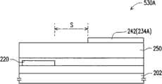
图6为本发明第四实施例的一种像素结构的上视图以及其局部放大示意图。请参照图6,在本实施例中,像素结构500除了前述的扫描线、第一数据线以及第一像素单元之外。在本实施例中,像素结构500更包括第二像素单元530B以及第二数据线520,如图6所示,像素结构500包括第一像素单元530A与第二像素单元530B,其中第一像素单元530A与第二像素单元530B位于第一数据线220与第二数据线520之间。具体来说,在像素结构500中,第二有源元件532B与第一有源元件232A电性连接在相同的扫描线210,而第二有源元件532B与第一有源元件232A电性则分别连接在不同的数据线。FIG. 6 is a top view and a partially enlarged schematic diagram of a pixel structure according to a fourth embodiment of the present invention. Please refer to FIG. 6 , in this embodiment, the pixel structure 500 is except for the aforementioned scan lines, first data lines and first pixel units. In this embodiment, the pixel structure 500 further includes a
请参照图6,第二像素单元530B包括第二有源元件532B以及第二像素电极534B,其中第二有源元件532B与扫描线210以及第二数据线520电性连接,而第二像素电极534B与第二有源元件532B电性连接。特别的是,如放大图所示,第二像素电极534B具有多个分支242,且分支242延伸至第一数据线220与第二数据线520上方并跨越数据线。6, the
更具体来说,图7A与图7B为分别沿着图6的像素结构的AA剖面线与BB剖面线的剖面示意图。请先参照图7A,在本实施例的第一像素单元530A中,第一像素电极234A的分支242与第一数据线220在基板202上的投影彼此分离,且第一像素电极234A与第一数据线220具有一间距S,而此间距S的范围至少为3微米,较佳例如为3微米至9微米。接着,请参照图7B,在第二像素单元530B中,第二像素电极534B具有多个分支242,且分支242延伸至第一数据线220与第二数据线520上方并跨越数据线,换句话说,第二像素电极534B的分支242自第二数据线520上方的一侧延伸至该数据线上方的相对侧,在一实施例中,第二像素电极534B的分支242自第二数据线520的凸出量L例如为2微米。More specifically, FIG. 7A and FIG. 7B are schematic cross-sectional views along the AA section line and BB section line of the pixel structure in FIG. 6 , respectively. Please refer to FIG. 7A first. In the
值得一提的是,当应用本实施例的像素结构500来进行显示时,第一像素单元530A作为主显示单元,而第二像素单元530B作为次显示单元,如此,可以消除第二像素电极534B邻近数据线处的不明确现象,使其减轻至观察者无法辨别的程度,或者完全消除。值得一提的是,第二像素单元530B是作为次显示单元,其操作灰阶通常较低,因此即使第二像素电极534B的分支242跨越第二数据线520上方并无信号相互干扰的疑虑,换句话说,以此像素结构500进行显示时具有较佳的显示质量。It is worth mentioning that when the pixel structure 500 of this embodiment is used for display, the
虽然在本实施例的像素结构500中,是以并用前述实施例的技术的方式进行说明,但设计者也可视产品需求而单独采本实施例的利用将第二像素单元的第二像素电极的分支延伸至相邻数据线上方并跨越该些数据线的方式来实现消除显示时的不明确现象、提升显示质量的效果,本发明不以此为限。Although in the pixel structure 500 of this embodiment, the description is made by using the technology of the foregoing embodiments together, but the designer can also independently adopt the second pixel electrode of the second pixel unit in this embodiment depending on the product requirements. The branch of the branch extends above the adjacent data lines and crosses these data lines to achieve the effects of eliminating ambiguity during display and improving display quality, and the present invention is not limited thereto.
当然,本实施例的第二像素电极534B可以采用描述在第一实施例中的第一像素电极234A的配置方式,以进一步消除显示时的不明确现象。具体来说,图8A为图6所绘示像素结构的另一种的局部放大示意图而图8B为图8A沿BB’剖面线的剖面示意图。请参照图8A与图8B,第二像素电极534B的分支242之间构成狭缝430。如图8A与图8B所示,第二像素电极534B也可以具有一大体平行扫描线210(绘示在图6)的条状图案240,在本实施例中,第二像素电极534B的条状图案240的一侧可与延伸在扫描线210的第二像素电极534B的分支242连接,而第二像素电极534B的条状图案240的另一侧与扫描线210部分重叠。具体来说,第二像素电极534B的条状图案240与扫描线210的重叠宽度为第二像素电极534B的条状图案240的宽度的40%~90%,其中条状图案240与该扫描线210的重叠宽度W1实质上为1.5um至15um。换句话说,令条状图案240与扫描线210的重叠宽度为W1、而令条状图案240未与扫描线210重叠的宽度为W2,其中条状图案240的宽度W则为W1与W2的总和。当像素结构500应用于超高开口率型(ultra high aperture)的设计时,W1与W2较佳的比例为4比1,可以充分降低漏光现象。另一方面,当像素结构500应用于彩色滤光膜直接整合在薄膜晶体管阵列基板(ColorFilter on Array,COA)或黑矩阵制作在薄膜晶体管阵列基板上(Black matrix onArray,BOA)的设计时,W1与W2较佳的比例为1比1时,可以充分降低漏光现象,进而得到较佳化的显示质量。在一实施例中,条状图案240与扫描线210的重叠宽度W1与条状图案240未与扫描线210重叠的宽度W2例如分别为2.5微米。Of course, the
综上所述,本发明的像素结构具有下列优点的至少其中之一或全部:In summary, the pixel structure of the present invention has at least one or all of the following advantages:
(一)本发明因在通过适当控制像素结构中像素电极的条状图案与扫描线重叠宽度之间的比例关系,可以降低像素结构在显示时的漏光现象,进而提升开口率。(1) The present invention can reduce the light leakage phenomenon of the pixel structure during display by appropriately controlling the proportional relationship between the stripe pattern of the pixel electrode and the overlapping width of the scanning lines in the pixel structure, thereby increasing the aperture ratio.
(二)本发明通过控制像素电极在彩色滤光层的开口处附近的设计型态,可以抑制像素结构在用以显示时,液晶分子在该处倾倒方向不明确(disclination)的现象。(2) By controlling the design of the pixel electrode near the opening of the color filter layer, the present invention can suppress disclination of liquid crystal molecules when the pixel structure is used for display.
(三)本发明的上电容电极是通过邻近数据线的周边的分支而与第一像素电极连接,因此可以抑制像素结构在用以显示时,液晶分子在该处倾倒方向不明确(disclination)的现象,进而获得较佳的显示质量。(3) The upper capacitive electrode of the present invention is connected to the first pixel electrode through a branch adjacent to the periphery of the data line, so that when the pixel structure is used for display, the direction of liquid crystal molecules tilting is unclear (disclination). Phenomenon, so as to obtain better display quality.
(四)本发明将像素结构的第二像素单元的像素电极的分支延伸至相邻数据线上方并跨越该些数据线,因此可以抑制像素结构在用以显示时,液晶分子在该处倾倒方向不明确(disclination)的现象,进而提供高质量化的显示。(4) In the present invention, the branch of the pixel electrode of the second pixel unit of the pixel structure is extended above the adjacent data lines and across these data lines, so that the liquid crystal molecules can be prevented from inverting the direction of the liquid crystal molecules when the pixel structure is used for display. Unclear (disclination) phenomenon, and then provide high-quality display.
虽然本发明已公开了上述实施例揭露,然而其并非用以限定本发明,任何所属技术领域中普通技术人员,在不脱离本发明的精神和范围内,应当能够作出一些更动与修改,因此本发明的保护范围当以权利要求书所限定的范围为准。Although the present invention has disclosed the disclosure of the above embodiments, it is not intended to limit the present invention. Any person skilled in the art should be able to make some changes and modifications without departing from the spirit and scope of the present invention. Therefore, The protection scope of the present invention shall be determined by the scope defined in the claims.
Claims (19)
Priority Applications (1)
| Application Number | Priority Date | Filing Date | Title |
|---|---|---|---|
| CN2009102619138ACN101726954B (en) | 2009-12-21 | 2009-12-21 | Pixel structure |
Applications Claiming Priority (1)
| Application Number | Priority Date | Filing Date | Title |
|---|---|---|---|
| CN2009102619138ACN101726954B (en) | 2009-12-21 | 2009-12-21 | Pixel structure |
Publications (2)
| Publication Number | Publication Date |
|---|---|
| CN101726954A CN101726954A (en) | 2010-06-09 |
| CN101726954Btrue CN101726954B (en) | 2011-11-16 |
Family
ID=42448020
Family Applications (1)
| Application Number | Title | Priority Date | Filing Date |
|---|---|---|---|
| CN2009102619138AActiveCN101726954B (en) | 2009-12-21 | 2009-12-21 | Pixel structure |
Country Status (1)
| Country | Link |
|---|---|
| CN (1) | CN101726954B (en) |
Families Citing this family (8)
| Publication number | Priority date | Publication date | Assignee | Title |
|---|---|---|---|---|
| CN102269898B (en)* | 2011-07-18 | 2013-11-06 | 深圳市华星光电技术有限公司 | Pixel electrode and liquid crystal display panel |
| CN102789099A (en)* | 2012-07-16 | 2012-11-21 | 北京京东方光电科技有限公司 | Liquid crystal display pixel structure, array substrate and liquid crystal display device |
| KR102069821B1 (en)* | 2013-07-03 | 2020-01-28 | 삼성디스플레이 주식회사 | Liquid crystal display |
| CN105446030B (en)* | 2014-09-01 | 2019-02-01 | 群创光电股份有限公司 | Liquid crystal display panel |
| CN104483791A (en)* | 2014-12-18 | 2015-04-01 | 深圳市华星光电技术有限公司 | Liquid crystal panel and liquid crystal display comprising same |
| TWI550320B (en)* | 2014-12-31 | 2016-09-21 | 友達光電股份有限公司 | Pixel structure |
| TWI562340B (en)* | 2015-09-15 | 2016-12-11 | Au Optronics Corp | Pixel structure and display panel |
| CN110992908A (en) | 2019-12-10 | 2020-04-10 | 深圳市华星光电半导体显示技术有限公司 | Pixel arrangement structure and display panel |
Citations (2)
| Publication number | Priority date | Publication date | Assignee | Title |
|---|---|---|---|---|
| CN101145568A (en)* | 2007-10-26 | 2008-03-19 | 友达光电股份有限公司 | Pixel structure and manufacturing method of liquid crystal display panel with pixel structure |
| CN101236337A (en)* | 2007-02-01 | 2008-08-06 | 中华映管股份有限公司 | pixel structure |
- 2009
- 2009-12-21CNCN2009102619138Apatent/CN101726954B/enactiveActive
Patent Citations (2)
| Publication number | Priority date | Publication date | Assignee | Title |
|---|---|---|---|---|
| CN101236337A (en)* | 2007-02-01 | 2008-08-06 | 中华映管股份有限公司 | pixel structure |
| CN101145568A (en)* | 2007-10-26 | 2008-03-19 | 友达光电股份有限公司 | Pixel structure and manufacturing method of liquid crystal display panel with pixel structure |
Also Published As
| Publication number | Publication date |
|---|---|
| CN101726954A (en) | 2010-06-09 |
Similar Documents
| Publication | Publication Date | Title |
|---|---|---|
| TWI406073B (en) | Pixel structure | |
| CN101726954B (en) | Pixel structure | |
| US10585313B2 (en) | Liquid crystal display device | |
| US11392002B2 (en) | Array substrate, display panel and display device | |
| US11774809B2 (en) | Liquid crystal display panel | |
| JP5246782B2 (en) | Liquid crystal device and electronic device | |
| US6856371B2 (en) | In plane fringe field switching mode LCD realizing high screen quality | |
| TWI392940B (en) | Pixel structure, touch display panel and liquid crystal display | |
| US20130229608A1 (en) | Liquid crystal display | |
| US7898624B2 (en) | Pixel array substrate and liquid crystal display | |
| CN109239969A (en) | Liquid crystal display panel | |
| WO2012147722A1 (en) | Liquid crystal display device | |
| JP6640252B2 (en) | LCD panel | |
| KR20160014848A (en) | Liquid crystal display device | |
| CN101561572B (en) | Liquid crystal display device | |
| US8730414B2 (en) | Liquid crystal display device including various embodiments of light-shielding line | |
| JP4407677B2 (en) | Horizontal electric field LCD panel | |
| CN101131522A (en) | LCD panel | |
| TWI493266B (en) | Pixel structure | |
| US6791653B2 (en) | In-plane switching mode liquid crystal display | |
| US7098978B2 (en) | Wide-viewing angle liquid crystal display | |
| US6933997B2 (en) | Liquid crystal display device and array substrate for the same | |
| CN101533190A (en) | Pixel structure and liquid crystal display panel | |
| US20040125304A1 (en) | Array substrate for use in in-plane switching mode liquid crystal display device | |
| CN114879419B (en) | Array substrate and display panel |
Legal Events
| Date | Code | Title | Description |
|---|---|---|---|
| C06 | Publication | ||
| PB01 | Publication | ||
| C10 | Entry into substantive examination | ||
| SE01 | Entry into force of request for substantive examination | ||
| C14 | Grant of patent or utility model | ||
| GR01 | Patent grant |