CN101711413B - Non-volatile memory device with individually controllable shielding plates between memory elements - Google Patents
Non-volatile memory device with individually controllable shielding plates between memory elementsDownload PDFInfo
- Publication number
- CN101711413B CN101711413BCN200880021966.6ACN200880021966ACN101711413BCN 101711413 BCN101711413 BCN 101711413BCN 200880021966 ACN200880021966 ACN 200880021966ACN 101711413 BCN101711413 BCN 101711413B
- Authority
- CN
- China
- Prior art keywords
- voltage
- barricade
- word line
- volatile memory
- couple
- Prior art date
- Legal status (The legal status is an assumption and is not a legal conclusion. Google has not performed a legal analysis and makes no representation as to the accuracy of the status listed.)
- Active
Links
Images


Classifications
- G—PHYSICS
- G11—INFORMATION STORAGE
- G11C—STATIC STORES
- G11C16/00—Erasable programmable read-only memories
- G11C16/02—Erasable programmable read-only memories electrically programmable
- G11C16/04—Erasable programmable read-only memories electrically programmable using variable threshold transistors, e.g. FAMOS
- G11C16/0483—Erasable programmable read-only memories electrically programmable using variable threshold transistors, e.g. FAMOS comprising cells having several storage transistors connected in series
- H—ELECTRICITY
- H10—SEMICONDUCTOR DEVICES; ELECTRIC SOLID-STATE DEVICES NOT OTHERWISE PROVIDED FOR
- H10B—ELECTRONIC MEMORY DEVICES
- H10B41/00—Electrically erasable-and-programmable ROM [EEPROM] devices comprising floating gates
- H10B41/10—Electrically erasable-and-programmable ROM [EEPROM] devices comprising floating gates characterised by the top-view layout
- H—ELECTRICITY
- H10—SEMICONDUCTOR DEVICES; ELECTRIC SOLID-STATE DEVICES NOT OTHERWISE PROVIDED FOR
- H10B—ELECTRONIC MEMORY DEVICES
- H10B41/00—Electrically erasable-and-programmable ROM [EEPROM] devices comprising floating gates
- H10B41/30—Electrically erasable-and-programmable ROM [EEPROM] devices comprising floating gates characterised by the memory core region
- H10B41/35—Electrically erasable-and-programmable ROM [EEPROM] devices comprising floating gates characterised by the memory core region with a cell select transistor, e.g. NAND
- H—ELECTRICITY
- H10—SEMICONDUCTOR DEVICES; ELECTRIC SOLID-STATE DEVICES NOT OTHERWISE PROVIDED FOR
- H10B—ELECTRONIC MEMORY DEVICES
- H10B69/00—Erasable-and-programmable ROM [EPROM] devices not provided for in groups H10B41/00 - H10B63/00, e.g. ultraviolet erasable-and-programmable ROM [UVEPROM] devices
- H—ELECTRICITY
- H10—SEMICONDUCTOR DEVICES; ELECTRIC SOLID-STATE DEVICES NOT OTHERWISE PROVIDED FOR
- H10D—INORGANIC ELECTRIC SEMICONDUCTOR DEVICES
- H10D89/00—Aspects of integrated devices not covered by groups H10D84/00 - H10D88/00
- H10D89/10—Integrated device layouts
- G—PHYSICS
- G11—INFORMATION STORAGE
- G11C—STATIC STORES
- G11C16/00—Erasable programmable read-only memories
- G11C16/02—Erasable programmable read-only memories electrically programmable
- G11C16/06—Auxiliary circuits, e.g. for writing into memory
- G11C16/10—Programming or data input circuits
Landscapes
- Engineering & Computer Science (AREA)
- Microelectronics & Electronic Packaging (AREA)
- Semiconductor Memories (AREA)
- Non-Volatile Memory (AREA)
Abstract
Description
Translated fromChinese技术领域technical field
本发明涉及非易失性存储器。The present invention relates to non-volatile memory.
背景技术Background technique
半导体存储器已日益普遍地用在各种电子装置中。例如,非易失性半导体存储器被用在蜂窝电话、数码相机、个人数字助理、移动计算装置、非移动计算装置和其他装置中。电可擦除可编程只读存储器(EEPROM)和闪存是位于最受欢迎的非易失性半导体存储器之列。对于闪存——其也是一种EEPROM——与传统的全特征的(full-featured)EEPROM相比,可以在一步中擦除整个存储器阵列或一部分存储器的内容。Semiconductor memories have become increasingly common in various electronic devices. For example, non-volatile semiconductor memory is used in cellular telephones, digital cameras, personal digital assistants, mobile computing devices, non-mobile computing devices, and other devices. Electrically Erasable Programmable Read-Only Memory (EEPROM) and flash memory are among the most popular non-volatile semiconductor memories. With flash memory—which is also a type of EEPROM—the contents of the entire memory array or a portion of the memory can be erased in one step compared to conventional full-featured EEPROMs.
传统EEPROM和闪存都使用位于半导体衬底中的沟道区之上并与之绝缘的浮置栅极(floating gate)。浮置栅极位于源极和漏极区之间。控制栅极在浮置栅极上提供并与之绝缘。由此形成的晶体管的阈值电压(VTH)通过被保留在浮置栅极中的电荷量来控制。即,由浮置栅极上电荷的水平控制在导通晶体管以允许在其源极和漏极之间导电之前必须施加到控制栅极的最小电压量。Both conventional EEPROM and flash memory use a floating gate that is positioned over and insulated from a channel region in a semiconductor substrate. The floating gate is located between the source and drain regions. The control gate is provided over and insulated from the floating gate. The threshold voltage (VTH ) of the resulting transistor is controlled by the amount of charge that is retained in the floating gate. That is, the minimum amount of voltage that must be applied to the control gate before the transistor is turned on to allow conduction between its source and drain is controlled by the level of charge on the floating gate.
一些EEPROM和闪存器件具有用于存储两个范围的电荷的浮置栅极,因而,存储元件可以在两个状态,例如擦除状态和编程状态之间编程/擦除。这样的闪存器件有时被称为二进制闪存器件,因为每个存储元件可存储一个比特的数据。Some EEPROM and flash memory devices have floating gates for storing two ranges of charge, thus, storage elements can be programmed/erased between two states, eg, an erased state and a programmed state. Such flash memory devices are sometimes referred to as binary flash memory devices because each storage element can store one bit of data.
通过识别多个不同的允许/有效编程阈值电压范围,实现多状态(也称为多级)闪存器件。每个不同的阈值电压范围对应于被编码到存储器装置中的数据比特组的预定值。例如,当每个存储器元件可被置于与四个不同阈值电压范围对应的四个离散电荷带之一中时,每个存储器元件可存储两比特数据。Multi-state (also referred to as multi-level) flash memory devices are implemented by identifying multiple different allowable/valid programming threshold voltage ranges. Each distinct threshold voltage range corresponds to a predetermined value for a set of data bits encoded into the memory device. For example, each memory element can store two bits of data when each memory element can be placed in one of four discrete charge bands corresponding to four different threshold voltage ranges.
典型地,在编程操作期间施加到控制栅极的编程电压VPGM被施加为幅度随时间增加的一系列脉冲。在一个可能的方式中,脉冲的幅度随着每个后续脉冲增加预定步长,例如0.2-0.4V。VPGM可被施加到闪存元件的控制栅极。在编程脉冲之间的时段中,执行校验操作。即,在连续编程脉冲之间读取被并行编程的一组元件中每个元件的编程电平,以确定它是否等于或大于元件正被编程到其的校验电平。对于多状态闪存元件的阵列,可对于元件的每个状态执行校验步骤,以确定元件是否已达到其数据关联的校验电平。例如,能够以四个状态存储数据的多状态存储器元件可能需要执行三个比较点的校验操作。Typically, the programming voltageVPGM applied to the control gate during a programming operation is applied as a series of pulses of increasing amplitude over time. In one possible manner, the amplitude of the pulse increases with each subsequent pulse by a predetermined step, eg 0.2-0.4V.VPGM can be applied to the control gate of the flash memory element. In the period between program pulses, a verify operation is performed. That is, the programming level of each element in a group of elements being programmed in parallel is read between successive programming pulses to determine whether it is equal to or greater than the verify level to which the element is being programmed. For arrays of multi-state flash memory elements, a verify step may be performed for each state of the element to determine whether the element has reached its data-associated verify level. For example, a multi-state memory element capable of storing data in four states may need to perform a verify operation with three compare points.
此外,当对EEPROM或闪存器件诸如NAND串(string)中的NAND闪存器件编程时,典型地,VPGM被施加到控制栅极,并且位线接地,使得电子从单元或存储器(memory)元件例如,存储(storage)元件的沟道注入浮置栅极中。当电子在浮置栅极中积累时,浮置栅极充负电,并且存储器元件的阈值电压升高,从而存储器元件被认为是在编程状态中。关于这样的编程的更多信息可在题为“Source Side Self Boosting Technique For Non-Volatile Memory”的美国专利6,859,397以及2005年2月3日公开的题为“Detecting OverProgrammed Memory”的美国专利申请公开2005/0024939中找到,两者都通过引用全文合并于此。Furthermore, when programming an EEPROM or flash memory device such as a NAND flash memory device in a NAND string, typicallyVPGM is applied to the control gate and the bit line is grounded so that electrons are transferred from the cell or memory element such as , the channel of the storage element is implanted into the floating gate. When electrons accumulate in the floating gate, the floating gate charges negatively and the threshold voltage of the memory element rises so that the memory element is considered to be in a programmed state. More information on such programming can be found in U.S. Patent 6,859,397, entitled "Source Side Self Boosting Technique For Non-Volatile Memory," and U.S. Patent Application Publication 2005, published Feb. 3, 2005, and entitled "Detecting OverProgrammed Memory." /0024939, both of which are hereby incorporated by reference in their entirety.
然而,随着器件尺寸缩小,带来各种挑战。例如,浮置栅极到浮置栅极耦合变得更成为问题,导致阈值电压分布扩大以及从控制栅极到浮置栅极的耦合率降低。However, as device dimensions shrink, various challenges arise. For example, floating gate-to-floating gate coupling becomes more problematic, resulting in widened threshold voltage distributions and reduced coupling ratios from control gates to floating gates.
发明内容Contents of the invention
本发明通过提供具有位于存储元件之间的可单独控制的屏蔽板的非易失性存储装置(storage),解决以上和其他问题。The present invention addresses the above and other problems by providing a non-volatile storage device (storage) having individually controllable shielding plates positioned between storage elements.
在一个实施例中,一种非易失性存储设备包括:衬底,其上形成非易失性存储元件;字线,与非易失性存储元件通信;以及屏蔽板,其中每个屏蔽板在与相邻字线相关联的不同的相邻非易失性存储元件之间延伸,每个屏蔽板是导电的并可独立控制。In one embodiment, a nonvolatile memory device includes: a substrate on which a nonvolatile memory element is formed; a word line in communication with the nonvolatile memory element; and shielding plates, wherein each shielding plate Extending between different adjacent non-volatile storage elements associated with adjacent word lines, each shield plate is conductive and independently controllable.
在另一实施例中,一种非易失性存储设备包括:衬底,其上形成非易失性存储元件,其中非易失性存储元件被布置在第一组和第二组中;字线,与第一组和第二组的非易失性存储元件通信;以及第一组屏蔽板,其中第一组屏蔽板中每个屏蔽板在与第一组非易失性存储元件的相邻字线相关联的不同的相邻非易失性存储元件之间延伸,是导电的并可独立控制。该设备还包括第二组屏蔽板,其中第二组屏蔽板中每个屏蔽板在与第二组非易失性存储元件的相邻字线相关联的不同的相邻非易失性存储元件之间延伸,是导电的并可独立控制。In another embodiment, a nonvolatile memory device includes: a substrate on which nonvolatile memory elements are formed, wherein the nonvolatile memory elements are arranged in a first group and a second group; lines in communication with the first and second sets of non-volatile storage elements; and a first set of shielding plates, wherein each shielding plate of the first set of shielding plates is in communication with the first set of non-volatile storage elements Different adjacent non-volatile storage elements associated with adjacent word lines extend between, are conductive and are independently controllable. The device also includes a second set of shielding plates, wherein each shielding plate of the second set of shielding plates is on a different adjacent non-volatile storage element associated with an adjacent word line of the second set of non-volatile storage elements extending between, are conductive and independently controllable.
在另一实施例中,非易失性存储设备包括:衬底,其上形成非易失性存储元件,其中非易失性存储元件被布置在第一组和第二组中;字线,与第一组和第二组的非易失性存储元件通信;以及第一组屏蔽板,其中第一组屏蔽板中的每个屏蔽板在与第一组非易失性存储元件的相邻字线相关联的不同的相邻非易失性存储元件之间延伸。该设备还包括第二组屏蔽板,其中第二组屏蔽板中每个屏蔽板在与第二组非易失性存储元件的相邻字线相关联的不同的相邻非易失性存储元件之间延伸。另外,屏蔽板是导电的并是可独立于各组屏蔽板中的其他屏蔽板控制的。In another embodiment, a nonvolatile memory device includes: a substrate on which nonvolatile memory elements are formed, wherein the nonvolatile memory elements are arranged in a first group and a second group; word lines, in communication with the first and second sets of non-volatile storage elements; and a first set of shielding plates, wherein each shielding plate in the first set of shielding plates is adjacent to the first set of non-volatile storage elements Word lines extend between different adjacent non-volatile storage elements associated with them. The device also includes a second set of shielding plates, wherein each shielding plate of the second set of shielding plates is on a different adjacent non-volatile storage element associated with an adjacent word line of the second set of non-volatile storage elements extend between. Additionally, the shields are conductive and controllable independently of the other shields in each set of shields.
在另一实施例中,非易失性存储设备包括:衬底,其上形成非易失性存储元件,其中非易失性存储元件被布置为组;以及屏蔽物(shield),其中每个屏蔽物在不同的相邻组的非易失性存储元件之间延伸,并且每个屏蔽物可独立控制以减少该屏蔽物在期间延伸的相邻组的非易失性存储元件之间的电磁耦合。In another embodiment, a nonvolatile memory device includes: a substrate on which nonvolatile memory elements are formed, wherein the nonvolatile memory elements are arranged in groups; and shields, each of which The shields extend between different adjacent sets of non-volatile storage elements, and each shield is independently controllable to reduce electromagnetic interference between adjacent sets of non-volatile storage elements during which the shield extends. coupling.
在一个实施例中,用于操作非易失性存储装置的方法包括:将编程电压施加到一组字线中的所选字线,其中字线与相关联的多个非易失性存储元件通信;以及在施加编程电压期间,将电压耦接到一组屏蔽板中的每个屏蔽板,其中每个屏蔽板是导电的并在与相邻字线相关联的不同的相邻非易失性存储元件之间延伸。In one embodiment, a method for operating a nonvolatile storage device includes applying a programming voltage to a selected word line of a set of word lines, wherein the word line is associated with a plurality of nonvolatile storage elements communicating; and, during application of the programming voltage, coupling a voltage to each shield plate of a set of shield plates, wherein each shield plate is conductive and operates on a different adjacent nonvolatile extended between memory elements.
在另一实施例中,用于操作非易失性存储装置的方法包括:将电压施加到一组字线中的所选字线,以用在感测一组非易失性存储元件中的至少一个非易失性存储元件的状况的感测操作中,其中字线与非易失性存储元件通信,并且所选字线与该至少一个非易失性存储元件通信。该方法还包括在施加电压期间,将电压耦接到一组屏蔽板,其中每个屏蔽板在与相邻字线相关联的不同的相邻非易失性存储元件之间延伸,以及该方法包括感测该至少一个非易失性存储元件的状况。In another embodiment, a method for operating a nonvolatile memory device includes applying a voltage to a selected one of a set of wordlines for sensing a voltage in a set of nonvolatile storage elements. In a sensing operation of a condition of at least one non-volatile storage element, wherein the word line is in communication with the non-volatile storage element, and the selected word line is in communication with the at least one non-volatile storage element. The method also includes, during the application of the voltage, coupling a voltage to a set of shield plates, wherein each shield plate extends between a different adjacent non-volatile storage element associated with an adjacent word line, and the method Including sensing a condition of the at least one non-volatile storage element.
在另一实施例中,用于操作非易失性存储装置的方法包括:通过将电压施加到与第一组非易失性存储元件通信的第一组字线并将电压施加到在与第一组字线中的相邻字线相关联的不同的相邻非易失性存储元件之间延伸的第一组屏蔽板,而执行关于第一组非易失性存储元件的操作。第一组非易失性存储元件与第二组非易失性存储元件形成在同一p阱上。该方法还包括,在执行该操作时,允许电压在与第二组非易失性存储元件通信的第二组字线上以及在与第二组字线中的相邻字线相关联的不同的相邻非易失性存储元件之间延伸的第二组屏蔽板上浮置。In another embodiment, a method for operating a non-volatile storage device includes applying a voltage to a first set of word lines in communication with a first set of non-volatile storage elements by applying a voltage to A first set of shield plates extending between different adjacent nonvolatile storage elements associated with adjacent wordlines in a set of wordlines to perform operations with respect to the first set of nonvolatile storage elements. The first set of non-volatile storage elements is formed on the same p-well as the second set of non-volatile storage elements. The method also includes, while performing the operation, allowing voltages to differ across a second set of word lines in communication with the second set of non-volatile storage elements and across a second set of word lines associated with adjacent word lines in the second set of word lines. A second set of shield plates extending between adjacent non-volatile storage elements of the Float Float.
在一个实施例中,用于制造非易失性存储设备的方法包括:在衬底上形成非易失性存储元件,其中非易失性存储元件被布置在第一组和第二组中;以及形成与第一组和第二组的非易失性存储元件通信的字线。该方法还包括形成第一组屏蔽板,其中第一组屏蔽板中的每个屏蔽板在与第一组的相邻字线相关联的不同的相邻非易失性存储元件之间延伸,形成第二组屏蔽板,其中第二组屏蔽板中每个屏蔽板在与第二组非易失性存储元件的相邻字线相关联的不同的相邻非易失性存储元件之间延伸。此外,多对屏蔽板由相关联的导电路径耦合,并且每对屏蔽板包括在第一组非易失性存储元件中的屏蔽板和在第二组非易失性存储元件中的相关联的屏蔽板。In one embodiment, a method for manufacturing a nonvolatile memory device includes: forming nonvolatile memory elements on a substrate, wherein the nonvolatile memory elements are arranged in a first group and a second group; And forming word lines in communication with the first and second sets of non-volatile storage elements. The method also includes forming a first set of shielding plates, wherein each shielding plate of the first set of shielding plates extends between different adjacent non-volatile storage elements associated with adjacent word lines of the first set, forming a second set of shielding plates, wherein each shielding plate of the second set of shielding plates extends between different adjacent non-volatile storage elements associated with adjacent word lines of the second set of non-volatile storage elements . In addition, pairs of shield plates are coupled by associated conductive paths, and each pair of shield plates includes a shield plate in the first set of non-volatile storage elements and an associated shield plate in the second set of non-volatile storage elements. shielding plate.
在另一实施例中,用于制造非易失性存储设备的方法包括:在衬底上形成非易失性存储元件;形成与非易失性存储元件通信的字线;以及形成屏蔽板,其中每个屏蔽板在与相邻字线相关联的不同的相邻非易失性存储元件之间延伸,并且每个屏蔽板是导电的并可独立控制。In another embodiment, a method for manufacturing a nonvolatile memory device includes: forming a nonvolatile memory element on a substrate; forming a word line communicating with the nonvolatile memory element; and forming a shielding plate, Each of the shield plates extends between a different adjacent nonvolatile storage element associated with an adjacent word line, and each shield plate is electrically conductive and independently controllable.
在另一实施例中,用于制造非易失性存储设备的方法包括:在衬底上形成非易失性存储元件,其中非易失性存储元件被布置在第一组和第二组中;形成与第一组和第二组的非易失性存储元件通信的多个字线;以及形成第一组屏蔽板,其中第一组屏蔽板中每个屏蔽板在与第一组非易失性存储元件的相邻字线相关联的不同的相邻非易失性存储元件之间延伸,是导电的并且能独立控制。该方法还包括形成第二组屏蔽板,其中第二组屏蔽板中每个屏蔽板在与第二组非易失性存储元件的相邻字线相关联的不同的相邻非易失性存储元件之间延伸,是导电的并且能独立控制。In another embodiment, a method for manufacturing a nonvolatile memory device includes forming nonvolatile memory elements on a substrate, wherein the nonvolatile memory elements are arranged in a first group and a second group ; forming a plurality of word lines in communication with the first and second sets of nonvolatile storage elements; and forming a first set of shielding plates, wherein each shielding plate in the first set of shielding plates is in communication with the first set of nonvolatile storage elements The volatile storage elements extend between different adjacent nonvolatile storage elements associated with adjacent word lines, are conductive and are independently controllable. The method also includes forming a second set of shielding plates, wherein each shielding plate of the second set of shielding plates is on a different adjacent nonvolatile storage element associated with an adjacent word line of the second set of nonvolatile storage elements. The elements extend between, are conductive and can be independently controlled.
在另一实施例中,用于制造非易失性存储设备的方法包括:在衬底上形成非易失性存储元件,其中非易失性存储元件被布置为组;形成控制线,其中每个控制线与相关联组的非易失性存储元件通信;以及形成屏蔽物,其中每个屏蔽物在不同的相邻组的非易失性存储元件之间延伸。此外,每个屏蔽物可独立控制以减少该屏蔽物所延伸的相邻组的非易失性存储元件之间的电磁耦合。In another embodiment, a method for manufacturing a nonvolatile memory device includes: forming nonvolatile memory elements on a substrate, wherein the nonvolatile memory elements are arranged in groups; forming control lines, wherein each control lines communicate with an associated set of non-volatile storage elements; and form shields, wherein each shield extends between a different adjacent set of non-volatile storage elements. Additionally, each shield is independently controllable to reduce electromagnetic coupling between adjacent groups of non-volatile storage elements across which the shield extends.
附图说明Description of drawings
图1是NAND串的俯视图。Figure 1 is a top view of a NAND string.
图2是图1的NAND串的等效电路图。FIG. 2 is an equivalent circuit diagram of the NAND string of FIG. 1 .
图3是NAND闪存存储元件的阵列的框图。3 is a block diagram of an array of NAND flash storage elements.
图4描绘了NAND串的横截面视图。Figure 4 depicts a cross-sectional view of a NAND string.
图5描绘了具有屏蔽板的NAND串的横截面视图,其中在存储元件之间的衬底中提供源极/漏极区。Figure 5 depicts a cross-sectional view of a NAND string with shielding plates, where source/drain regions are provided in the substrate between storage elements.
图6描绘了具有屏蔽板的NAND串的横截面视图,其中在存储元件之间的衬底中不提供源极/漏极区。Figure 6 depicts a cross-sectional view of a NAND string with shielding plates, where no source/drain regions are provided in the substrate between storage elements.
图7a描绘了分层半导体器件,示出了横跨NAND串的横截面视图。Figure 7a depicts a layered semiconductor device showing a cross-sectional view across a NAND string.
图7b描绘了沿着图7a的分层半导体器件的NAND串的视图,其中施加和构图了(pattern)光刻胶(photoresist)层。Figure 7b depicts a view along a NAND string of the layered semiconductor device of Figure 7a with a photoresist layer applied and patterned.
图7c描绘了光刻胶瘦化(slimming)后的图7b的分层半导体器件。Figure 7c depicts the layered semiconductor device of Figure 7b after photoresist slimming.
图7d描绘了SiN蚀刻和光刻胶剥除后的图7c的分层半导体器件。Figure 7d depicts the layered semiconductor device of Figure 7c after SiN etch and photoresist stripping.
图7e描绘了SiO2沉积后的图7d的分层半导体器件。Figure 7e depicts the layered semiconductor device of Figure 7d afterSiO2 deposition.
图7f描绘了在提供了用于选择栅极的光刻胶掩模后的图7e的分层半导体器件。Figure 7f depicts the layered semiconductor device of Figure 7e after providing a photoresist mask for the select gates.
图7g描绘了SiO2蚀刻和光刻胶剥除后的图7f的分层半导体器件。Figure 7g depicts the layered semiconductor device of Figure 7f afterSiO2 etching and photoresist stripping.
图7h描绘了SiN湿蚀刻后的图7g的分层半导体器件。Figure 7h depicts the layered semiconductor device of Figure 7g after a SiN wet etch.
图7i描绘了多晶硅(poly)蚀刻后的图7h的分层半导体器件。Figure 7i depicts the layered semiconductor device of Figure 7h after polysilicon (poly) etch.
图7j描绘了O-N-O和多晶硅蚀刻后的图7i的分层半导体器件。Figure 7j depicts the layered semiconductor device of Figure 7i after O-N-O and polysilicon etch.
图7k描绘了在通过多晶硅沉积和CMP形成屏蔽板后的图7j的分层半导体器件。FIG. 7k depicts the layered semiconductor device of FIG. 7j after formation of shield plates by polysilicon deposition and CMP.
图8a描绘了图7b的分层半导体器件的俯视图。Figure 8a depicts a top view of the layered semiconductor device of Figure 7b.
图8b描绘了图7c的分层半导体器件的俯视图。Figure 8b depicts a top view of the layered semiconductor device of Figure 7c.
图8c描绘了图7d的分层半导体器件的俯视图。Figure 8c depicts a top view of the layered semiconductor device of Figure 7d.
图8d描绘了图7f的分层半导体器件的俯视图。Figure 8d depicts a top view of the layered semiconductor device of Figure 7f.
图8e描绘了图7g的分层半导体器件的俯视图。Figure 8e depicts a top view of the layered semiconductor device of Figure 7g.
图8f描绘了图7h的分层半导体器件的俯视图。Figure 8f depicts a top view of the layered semiconductor device of Figure 7h.
图8g描绘了从图8f的装置形成的分层半导体器件的俯视图,示出了由两组存储元件共享的字线触点和屏蔽板触点。Figure 8g depicts a top view of a layered semiconductor device formed from the device of Figure 8f, showing word line contacts and shield plate contacts shared by two sets of memory elements.
图8h描绘了替代分层半导体器件的俯视图,示出了用于每组存储元件的共享的字线触点和分离的屏蔽板触点。Figure 8h depicts a top view of an alternative layered semiconductor device showing shared word line contacts and separate shield plate contacts for each set of storage elements.
图8i描绘了替代分层半导体器件的俯视图,示出了用于每组存储元件的分离的字线触点和屏蔽板触点。Figure 8i depicts a top view of an alternative layered semiconductor device showing separate word line contacts and shield plate contacts for each set of storage elements.
图9描绘了存储元件的四个块,其中由一对块共享字线和屏蔽板。Figure 9 depicts four blocks of storage elements, where word lines and shield plates are shared by a pair of blocks.
图10描绘了用于制造具有屏蔽板的非易失性存储装置的工艺(process)。FIG. 10 depicts a process for fabricating a nonvolatile memory device with a shield plate.
图11是描述用于编程非易失性存储器的方法的一个实施例的流程图。Figure 11 is a flowchart describing one embodiment of a method for programming non-volatile memory.
图12描绘了在编程期间施加到非易失性存储元件的控制栅极的示例脉冲串。12 depicts an example pulse train applied to the control gates of non-volatile storage elements during programming.
图13是描述用于读取非易失性存储器的处理的一个实施例的流程图。Figure 13 is a flowchart describing one embodiment of a process for reading non-volatile memory.
具体实施方式Detailed ways
本发明提供了具有位于存储元件之间的可单独控制的屏蔽板的非易失性存储装置。The present invention provides a non-volatile memory device with individually controllable shielding plates between memory elements.
适合于实现本发明的存储器系统的一个例子使用NAND闪存结构,其包括在两个选择栅极之间串联布置多个晶体管。串联的晶体管和选择栅极被称为NAND串(string)。图1是示出一个NAND串的俯视图。图2是其等效电路。图1和图2描绘的NAND串包括四个晶体管100、102、104和106,串联并夹在第一选择栅极120和第二选择栅极122之间。选择栅极120选通(gate)到位线126的NAND串连接。选择栅极122选通到源极线128的NAND串连接。通过将合适的电压施加到控制栅极120CG来控制选择栅极120。通过将合适的电压施加到控制栅极122CG来控制选择栅极122。晶体管100、102、104和106的每个具有控制栅极和浮置栅极。晶体管100具有控制栅极100CG和浮置栅极100FG。晶体管102包括控制栅极102CG和浮置栅极102FG。晶体管104包括控制栅极104CG和浮置栅极104FG。晶体管106包括控制栅极106CG和浮置栅极106FG。控制栅极100CG连接到字线WL3(或由字线WL3的一部分提供),控制栅极102CG连接到字线WL2,控制栅极104CG连接到字线WL1,而控制栅极106CG连接到字线WL0。在一个实施例中,晶体管100、102、104和106每个都是存储元件,也被称为存储器单元。在其他实施例中,存储元件可包括多个晶体管,并且可以不同于图1和图2所描绘的。选择栅极120连接到选择线SGD。选择栅极122连接到选择线SGS。One example of a memory system suitable for implementing the present invention uses a NAND flash memory structure that includes multiple transistors arranged in series between two select gates. Transistors and select gates connected in series are called NAND strings. FIG. 1 is a top view showing one NAND string. Figure 2 is its equivalent circuit. The NAND string depicted in FIGS. 1 and 2 includes four
图3是描绘三个NAND串的电路图。使用NAND结构的闪存系统的典型结构体系将包括数个NAND串。例如,示出了具有多得多的NAND串的存储器阵列中的三个NAND串320、340和360。每个NAND串包括两个选择栅极和四个存储元件。尽管为了简单例示了四个存储元件,但现代的NAND串可具有多达例如32或64个存储元件。Figure 3 is a circuit diagram depicting three NAND strings. A typical architecture for a flash memory system using a NAND structure will include several NAND strings. For example, three
例如,NAND串320包括选择栅极322和327以及存储元件323-326,NAND串340包括选择栅极342和347以及存储元件343-346,NAND串360包括选择栅极362和367以及存储元件363-366。每个NAND串通过其选择栅极(例如,选择栅极327、347或367)连接到源极线。选择线SGS用来控制源极侧选择栅极。各个NAND串320、340和360通过选择栅极322、342、362等中的选择晶体管,连接到各自位线321、341和361。这些选择晶体管由漏极选择线SGD控制。在其他实施例中,选择线在NAND串之间不必是共同的;即,可以为不同的NAND串提供不同的选择线。字线WL3连接到存储元件323、343和363的控制栅极。字线WL2连接到存储元件324、344和364的控制栅极。字线WL1连接到存储元件325、345和365的控制栅极。字线WL0连接到存储元件326、346和366的控制栅极。每个位线和各自的NAND串构成存储元件的阵列或组的列。字线(WL3、WL2、WL1、WL0)构成阵列或组的行。每个字线连接行中每个存储元件的控制栅极。或者,可由字线本身提供控制栅极。例如,字线WL2提供存储元件324、344和364的控制栅极。实践中,一条字线上可存在数千个存储元件。For example,
每个存储元件可存储数据。例如,当存储一比特的数字数据时,存储元件的可能的阈值电压(VTH)的范围被分为两个范围,它们被分配了逻辑数据“1”和“0”。在NAND型闪存的一个例子中,VTH在存储元件被擦除后为负,并且被定义为逻辑“1”。编程操作后的VTH为正,并且被定义为逻辑“0”。当VTH为负并尝试读取时,存储元件将导通以表示正存储逻辑“1”。当VTH为正并尝试读取操作时,存储元件不导通,这表示存储了逻辑“0”。存储元件还可存储多级(level)信息,例如,多个比特的数字数据。在此情况下,VTH值的范围被分为数据级的数目。例如,如果存储四级信息,则将存在被分配给数据值“11”、“10”、“01”和“00”的四个VTH范围。在NAND型存储器的一个例子中,擦除操作后的VTH为负并被定义为“11”。正的VTH值用于“10”、“01”和“00”的状态。被编程到存储元件中的数据和元件的阈值电压范围之间的具体关系依赖于存储元件所采用的数据编码方案。例如,美观专利号6,222,762和美国专利申请公开2004/0255090描述了用于多状态闪存存储元件的各种数据编码方案,两者通过引用全文合并于此。Each storage element can store data. For example, when storing one bit of digital data, the range of possible threshold voltages (VTH ) of a storage element is divided into two ranges, which are assigned logical data "1" and "0". In one example of NAND-type flash memory, VTH is negative after the storage element is erased and is defined as a logic "1".VTH after a program operation is positive and is defined as a logic “0”. When VTH is negative and a read is attempted, the storage element will turn on to indicate that a logic "1" is being stored. When VTH is positive and a read operation is attempted, the storage element does not conduct, which indicates a logic "0" is stored. The storage element may also store multiple levels of information, eg, multiple bits of digital data. In this case, the range ofVTH values is divided into the number of data levels. For example, if four levels of information are stored, there will be four VTH ranges assigned to the data values "11", "10", "01" and "00". In an example of a NAND type memory,VTH after an erase operation is negative and defined as "11". Positive VTH values are used for the "10", "01" and "00" states. The specific relationship between the data programmed into a storage element and the threshold voltage range of the element depends on the data encoding scheme employed by the storage element. For example, Aesthetic Patent No. 6,222,762 and US Patent Application Publication 2004/0255090 describe various data encoding schemes for multi-state flash memory storage elements, both of which are hereby incorporated by reference in their entirety.
NAND型闪存及其操作的相关例子在美国专利号5,386,422、5,522,580、5,570,315、5,774,397、6,046,935、6,456,528和6,522,580中提供,它们每个通过引用合并于此。Related examples of NAND-type flash memory and its operation are provided in US Patent Nos. 5,386,422, 5,522,580, 5,570,315, 5,774,397, 6,046,935, 6,456,528, and 6,522,580, each of which is incorporated herein by reference.
当对闪存存储元件编程时,编程电压被施加到存储元件的控制栅极,并且与存储元件相关联的位线被接地。来自沟道的电子被注入到浮置栅极中。当电子在浮置栅极中积累时,浮置栅极充负电,并且存储器元件的阈值电压升高。为将编程电压施加到正被编程的存储元件的控制栅极,该编程电压被施加到合适的字线上。如上所述,每个NAND串中的一个存储元件共享相同的字线。例如,当对图3的存储元件324编程时,编程电压也被施加到存储元件344和364的控制栅极。When programming a flash storage element, a programming voltage is applied to the control gate of the storage element, and the bit line associated with the storage element is grounded. Electrons from the channel are injected into the floating gate. When electrons accumulate in the floating gate, the floating gate is negatively charged, and the threshold voltage of the memory element rises. To apply a programming voltage to the control gate of the storage element being programmed, the programming voltage is applied to the appropriate word line. As mentioned above, one storage element in each NAND string shares the same word line. For example, when programming
然而,在其他NAND串的编程期间,可能在禁用的(inhibited)NAND串处发生编程干扰,有时在被编程的NAND串自身处发生编程干扰。当未选的非易失性存储元件的阈值电压由于其他非易失性存储元件的编程而偏移(shift)时,发生编程干扰。编程干扰可能在前面编程的存储元件或还未被编程的擦除存储元件上发生。各种编程干扰机制可能限制诸如NAND闪存的非易失性存储器件的可用操作窗口。However, program disturb may occur at the inhibited NAND string, and sometimes at the programmed NAND string itself, during programming of other NAND strings. Program disturb occurs when the threshold voltage of an unselected non-volatile storage element is shifted due to programming of other non-volatile storage elements. Program disturb can occur on previously programmed storage elements or on erased storage elements that have not been programmed. Various program disturb mechanisms can limit the available operating window of non-volatile memory devices such as NAND flash memory.
例如,如果禁用NAND串320(例如,其是不包含当前正编程的存储元件的未选择的NAND串)并且NAND串340正被编程(例如,其是包含当前正编程的存储元件的选择的NAND串)时,可能在NAND串320处发生编程干扰。例如,如果流通电压(pass voltage)VPASS为低,则不会很好地对禁用的NAND串的沟道升压(boost),并且未选择的NAND串的所选字线可能被意外地编程。在另一可能的场景中,可通过栅极感应漏极漏电(GateInduced Drain Leakage,GIDL)或其他漏电机制降低升压的电压,导致同样的问题。其他效应,诸如由于与后面被编程的其他相邻存储元件的电容耦合而导致的在电荷存储元件的VTH中的偏移,也可能引起编程干扰。可通过这里描述的屏蔽板配置和控制技术降低编程干扰。For example, if
图4描绘了NAND串的横截面视图。该视图被简化且未按比例。NAND串400包括在衬底490上形成的源极侧选择栅极406、漏极侧选择栅极424和八个存储元件408、410、412、414、416、418、420和422。这些组件可在p阱区492上形成,p阱区492本身在p型衬底区496的n阱区494中形成。这些区一起成为衬底490的一部分。n阱也可在p衬底上形成。除了具有电势VBL的位线426之外,还提供具有电视VSOURCE的源极供电线404。根据正被执行的操作,例如,编程、感测(读取或校验)或擦除,字线接收相应电压。另外,回想起存储元件的控制栅极可作为字线的一部分来提供。例如,WL0、WL1、WL2、WL3、WL4、WL5、WL6和WL7可分别由(via)存储元件408、410、412、414、416、418、420和422的控制栅极而延伸。在一个方法中,通过在形成存储元件之后掺杂(dope)p阱区492,而在存储元件之间提供源极/漏极区,其例子在430处示出。字线或非易失性存储元件的源极侧是指面对NAND串的源极端例如在源极供电线404处的侧,而字线或非易失性存储元件的漏极侧是指面对NAND串的漏极端例如在位线426处的侧。Figure 4 depicts a cross-sectional view of a NAND string. The view is simplified and not to scale. NAND string 400 includes source side
图5描绘了具有屏蔽板的NAND串的横截面视图,其中在存储元件之间的衬底中提供源极/漏极区。这里,由导电材料提供多个屏蔽板,以提供相邻非易失性存储元件的浮置栅极之间的电磁辐射的屏蔽。导电材料可包括金属,如W或Ta,其可与势垒(barrier)金属使用,诸如WN、TaN或TiN。导电材料可包括掺杂多晶硅或硅化物,如WSi、TiSi、CoSi或NiSi。例如,在SGS 406和存储元件408之间提供屏蔽板SP0500,在存储元件408和410之间提供屏蔽板SP1502,在存储元件410和412之间提供屏蔽板SP2504,在存储元件412和414之间提供屏蔽板SP3506,在存储元件414和416之间提供屏蔽板SP4508,在存储元件416和418之间提供屏蔽板SP5510,在存储元件418和420之间提供屏蔽板SP6512,在存储元件420和422之间提供屏蔽板SP7514,并且在存储元件422和SGD 424之间提供屏蔽板SP8516。每个屏蔽板或部件可位于与相邻字线相关联的相邻存储元件的浮置栅极之间。该配置例如降低了在读取或编程操作期间浮置栅极到浮置栅极的耦合。注意,屏蔽板不必如图所描绘地延伸到所述存储元件/字线的顶部。然而,每个屏蔽板可延伸到或超出存储元件/字线的顶部,以便还降低控制栅极/字线到浮置栅极的耦合。在一种方式中,屏蔽板可具有大体上矩形的横截面。Figure 5 depicts a cross-sectional view of a NAND string with shielding plates, where source/drain regions are provided in the substrate between storage elements. Here, the plurality of shielding plates are provided by a conductive material to provide shielding of electromagnetic radiation between floating gates of adjacent non-volatile memory elements. Conductive materials may include metals such as W or Ta, which may be used with barrier metals such as WN, TaN or TiN. The conductive material may include doped polysilicon or suicide, such as WSi, TiSi, CoSi or NiSi. For example, shielding plate SP0500 is provided between
屏蔽板可以是可独立控制的,以通过将期望的电压耦接到每个屏蔽板,来优化它们在编程、感测(读取/校验)和擦除操作期间的效果。这是超越使用可共同控制的屏蔽板的方式的优势。另外,屏蔽板可允许使用降低的编程电压,因为它们能提供到正编程的存储元件的浮置栅极的某种电压耦合。结果,减少了编程干扰。The shields can be independently controllable to optimize their effectiveness during program, sense (read/verify) and erase operations by coupling desired voltages to each shield. This is an advantage over the approach of using jointly controllable shielding panels. Additionally, the shielding plates can allow the use of reduced programming voltages because they can provide some voltage coupling to the floating gate of the storage element being programmed. As a result, program disturb is reduced.
图6描绘了具有屏蔽板的NAND串的横截面视图,其中在存储元件之间的衬底中不提供源极/漏极区。在一个实施例中,不必在衬底的p阱区492中提供源极/漏极区,因为由于屏蔽板可提供存储元件之间的场感应导电性(field induced conductivity)。例如,在诸如读取或校验的感测操作期间,当所选存储元件处于导通/导电状态时,在NAND串中建立导电路径。可以在位线触点(contact)和单元源极触点之间经由漏极选择栅极、屏蔽板、字线/控制栅极和源极选择栅极形成的沟道(channel)建立这样的导电路径,例如,从选择栅极SGD 424到SP8516、到WL7、到SP7514、到WL6、到SP6512等,直到到达选择栅极SGS406和源极。基本上,当诸如大约4-5V的合适的电压施加到屏蔽板并且例如VSS=0V施加到字线时,在存储元件之间形成虚拟接合(virtual junction)。由此,感测操作不依赖于衬底中的导电路径。另外,因为屏蔽板是独立可控制的,所以可根据控制方案最优地调整它们的电压。使用这样的虚拟接合也有助于防止在不提供源极/漏极区的情况下的短沟道效应(short channel effect)。此外,消除对源极/漏极区的需要避免了制造工艺中的相应步骤。Figure 6 depicts a cross-sectional view of a NAND string with shielding plates, where no source/drain regions are provided in the substrate between storage elements. In one embodiment, it is not necessary to provide source/drain regions in the p-well region 492 of the substrate because the shielding plate can provide field induced conductivity between the storage elements. For example, during a sensing operation such as a read or verify, a conductive path is established in a NAND string when a selected storage element is in an on/conductive state. Such conduction can be established between the bit line contact and the cell source contact via the channel formed by the drain select gate, shield plate, word line/control gate, and source select gate. Path, for example, from
为了通过存储元件和屏蔽板之间的场感应导电性建立虚拟接合,正电压被施加到屏蔽板和存储元件。然而,由于屏蔽板电压到浮置栅极的耦合,屏蔽板电压将影响所选字线读取电压。该耦合将与屏蔽板电压×可能为大约5至15%的耦合率(coupling ratio)C(SP-FG/总FG)成比例。如果屏蔽板电压为高,则所选字线读取电压将增高。为降低虚源极-漏极接合(junction),应使用较高的屏蔽板电压,而为了降低所选字线读取电压,应使用较低的屏蔽板电压。为解决此冲突,在一种可能的方式中,可在交替的屏蔽板上交替的较高和较低屏蔽板电压(分别为VRSPH和VRSPL)。然而,还可以在所有屏蔽板上使用共同的屏蔽板电压(VRSP)。In order to establish a virtual junction through field-induced conductivity between the memory element and the shield, a positive voltage is applied to the shield and the memory element. However, due to the coupling of the shield voltage to the floating gate, the shield voltage will affect the selected word line read voltage. The coupling will be proportional to shield voltage x coupling ratio C(SP-FG/total FG), which may be about 5 to 15%. If the shield voltage is high, the selected word line read voltage will be high. To reduce virtual source-drain junctions, higher shield voltages should be used, and to lower selected word line read voltages, lower shield voltages should be used. To resolve this conflict, in one possible way, higher and lower shield plate voltages (VRSPH and VRSPL, respectively) can be alternated on alternate shield plates. However, it is also possible to use a common shield voltage (VRSP) on all shields.
现在讨论用于制造具有屏蔽板的非易失性存储装置的工艺。A process for fabricating a nonvolatile memory device with a shield plate is now discussed.
图7a描绘了分层(layer)半导体器件,示出了横跨(across)NAND串的横截面视图。描绘了制造的中间阶段。至此点的装置的形成可遵循传统的技术,其中在衬底712上形成第一介电层710(例如,栅极氧化物层),接着在第一介电层710上形成第一多晶硅(poly)层708。被掺杂从而导电的第一多晶硅层708用来形成存储元件的浮置栅极。通过构图(pattern)衬底712和蚀刻通过第一多晶硅层708和第一介电层710的沟槽,形成浅沟槽隔离(Shallowtrench isolation,STI)结构714。沟槽还延伸到衬底712中。用STI材料(诸如SiO2的合适的介电材料)填充沟槽,以提供NAND串之间的电绝缘。由此,STI材料的条带形成了横跨被第一多晶硅层708的条带分离的衬底712(在垂直于图的横截面的方向上)延伸的STI结构714。Figure 7a depicts a layered semiconductor device showing a cross-sectional view across a NAND string. Intermediate stages of manufacture are depicted. Formation of the device to this point may follow conventional techniques in which a first dielectric layer 710 (eg, a gate oxide layer) is formed on a substrate 712, followed by a first polysilicon layer formed on the first dielectric layer 710 (poly) layer 708 . The first polysilicon layer 708, which is doped to be conductive, is used to form the floating gate of the storage element. A shallow trench isolation (STI) structure 714 is formed by patterning the substrate 712 and etching trenches through the first polysilicon layer 708 and the first dielectric layer 710 . The trench also extends into the substrate 712 . The trenches are filled with STI material (a suitable dielectric material such as SiO2 ) to provide electrical isolation between the NAND strings. Thus, the strips of STI material form STI structures 714 extending across (in a direction perpendicular to the cross-section of the figure) the substrate 712 separated by the strips of the first polysilicon layer 708 .
接着,在多晶硅层708上提供诸如O-N-O层的第二介电层706。O-N-O层是由硅氧化物、硅氮化物和硅氧化物形成的三层电介质。沉积第二多晶硅层704,其覆盖(overlie)STI结构714和第一多晶硅层708的条带。也被掺杂和导电的第二多晶硅层704通过第二介电层706与第一多晶硅层708的条带分离开。第二多晶硅层704用于形成字线和存储元件的控制栅极。在第二多晶硅层704上形成掩模层702。在此情况下,掩模层702由诸如硅氮化物(SiN)的电介质形成,但也可使用其他合适的掩模材料。Next, a
图7b描绘了沿着图7a的分层半导体器件的NAND串的视图,其中施加和构图了光刻胶层。图7b示出了沿着与图7a的横截面成直角的方向上的图7a的NAND阵列的横截面。由此,图7b示出了横截面形式的第一多晶硅层708的单个条带,其中第二多晶硅层704覆盖该条带。图7b还示出了覆盖掩模层702的部分光刻胶(PR)。通过施加光刻胶的毯状层(blanket layer)然后使用平版印刷工艺构图光刻胶,而形成构图后的光刻胶层716。在一种方式中,通过曝光于UV(紫外)光来构图光刻胶,但是也可使用其他构图工艺,如电子束(e-beam)平版印刷术。Figure 7b depicts a view along a NAND string of the layered semiconductor device of Figure 7a with a photoresist layer applied and patterned. Figure 7b shows a cross-section of the NAND array of Figure 7a along a direction at right angles to the cross-section of Figure 7a. Thus, Figure 7b shows a single strip of the first polysilicon layer 708 in cross-section, with the second polysilicon layer 704 covering the strip. FIG. 7 b also shows a portion of photoresist (PR) covering the
图7c描绘了光刻胶瘦化(slimming)后的图7b的分层半导体器件。光刻胶瘦化包括对光刻胶的一部分进行蚀刻,以移除至少一些光刻胶并且使得部分光刻胶更窄(narrow)。对于此步骤,可使用传统的蚀刻法,如干蚀刻。Figure 7c depicts the layered semiconductor device of Figure 7b after photoresist slimming. Resist thinning includes etching a portion of the photoresist to remove at least some of the photoresist and make portions of the photoresist narrower. For this step, conventional etching methods such as dry etching can be used.
图7d描绘了SiN蚀刻和光刻胶剥除后的图7c的分层半导体器件。在光刻胶瘦化后,使用光刻胶的瘦化部分来构图下面的SiN掩模层702。进行蚀刻使得移除掩模层702的未曝光部分。然后移除光刻胶716的剩余部分。图7d示出了沿着与图7c相同的横截面的所得的结构。当到达第二多晶硅层704时停止蚀刻。Figure 7d depicts the layered semiconductor device of Figure 7c after SiN etch and photoresist stripping. After the photoresist is thinned, the thinned portion of the photoresist is used to pattern the underlying
图7e描绘了二氧化硅(SiO2)沉积后的图7d的分层半导体器件。SiO2层718被形成为覆盖SiN层702的掩模部分和第二多晶硅层704的曝光区域的第三介电层。在一种方式中,可通过诸如化学汽相沉积(Chemical VaporDeposition,CVD)的传统工艺形成为毯状层的SiO2层718可以比介电层706和710更厚。SiO2层718沿着第二多晶硅的曝光部分并沿着掩模层702的顶面和侧壁延伸。Figure 7e depicts the layered semiconductor device of Figure7d after silicon dioxide (SiO2) deposition. A SiO2 layer 718 is formed as a third dielectric layer covering the masked portions of the
图7f描绘了提供用于选择栅极的光刻胶掩模后的图7e的分层半导体器件。可通过用光刻胶遮盖(cover)结构然后使用平版印刷工艺构图光刻胶以移除不需要的部分光刻胶,来形成掩模的光刻胶部分719和720。光刻胶部分719和720在直接覆盖第二多晶硅层704的SiO2层718的部分上方延伸。然后进行蚀刻以移除SiO2层718的某些曝光部分。该光刻胶掩模还可用于后面形成字线和屏蔽板触点的区域。Figure 7f depicts the layered semiconductor device of Figure 7e after providing a photoresist mask for the select gate. The photoresist portions 719 and 720 of the mask may be formed by covering the structure with photoresist and then patterning the photoresist using a lithographic process to remove unwanted portions of the photoresist. Photoresist portions 719 and 720 extend over portions of SiO2 layer 718 directly overlying second polysilicon layer 704 . Etching is then performed to remove some exposed portions of the SiO2 layer 718 . This photoresist mask can also be used in areas where the wordlines and shield contacts will be formed later.
图7g描绘了SiO2蚀刻和光刻胶剥除后的图7f的分层半导体器件。在一种方式中,使用诸如反应离子蚀刻(Reactive Ion Etching,RIE)的各向异性蚀刻,使得SiO2层718在某些地方被蚀刻穿,而部分SiO2层718沿着SiN掩模部分702的侧壁保留,作为侧壁隔板(spacer)。侧壁隔板的尺寸由SiO2层718的厚度和所使用的各向异性蚀刻的性质确定。在完成蚀刻后,还执行光刻胶剥除,以移除光刻胶部分719和720。以后建立选择栅极线和字线的位置的侧壁隔板不需要分离的对齐(separate alignment)。Figure 7g depicts the layered semiconductor device of Figure 7f afterSiO2 etching and photoresist stripping. In one approach, anisotropic etching such as reactive ion etching (Reactive Ion Etching, RIE) is used such that the SiO2 layer 718 is etched through in certain places, while portions of the SiO2 layer 718 are along the
图7h描绘了在湿蚀刻以移除SiN层702的部分由此留下SiO2层718的部分处于覆盖第二多晶硅层704的位置之后的图7g的分层半导体器件。接着,使用SiO2层718的保留部分作为蚀刻掩模以构图下面的层以形成存储器阵列。FIG. 7h depicts the layered semiconductor device of FIG. 7g after a wet etch to remove portions of
具体地,图7i描绘了在执行蚀刻步骤以蚀刻穿过多晶硅层704并在O-N-O层706停止后的图7h的分层半导体器件。In particular, FIG. 7i depicts the layered semiconductor device of FIG. 7h after performing an etching step to etch through polysilicon layer 704 and stop at
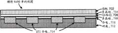
图7j描绘了O-N-O和多晶硅蚀刻后的图7i的分层半导体器件。这里,蚀刻O-N-O层706、多晶硅层708和介电层710,在衬底712停止。该蚀刻步骤将多晶硅层704分离为分离的字线,并将多晶硅层708分离为分离的浮置栅极。字线形成控制栅极,其中它们覆盖各自存储元件721中的浮置栅极。类似地形成选择栅极723和724。因为通过相同的蚀刻步骤形成字线和浮置栅极,所以它们是自对齐的(self aligned)。还可通过将掺杂剂植入衬底712的曝光区域中,来提供存储元件721之间的源极/漏极区722。在一种方式中,这些曝光区域位于浮置栅极之间,从而它们连接NAND串的存储元件。Figure 7j depicts the layered semiconductor device of Figure 7i after O-N-O and polysilicon etch. Here,
图7k描绘了通过多晶硅沉积和化学机械研磨(chemical mechanicalpolishing,CMP)形成屏蔽板后的图7j的分层半导体器件。介电层721被沉积在分层结构上,并且多晶硅沉积在该介电层上。在示例实现方式中,介电层包括SiO2、SiO2-SiN-SiO2、SiO2-AlO-SiO2或SiO2-HfO-SiO2,具有大约9-12nm的物理厚度以及大约7-11nm的有效厚度。进行CMP以平滑(planarize)表面。可掺杂多晶硅以提供期望的导电性。接着,可用诸如厚介电层的保护层或其他保护材料遮盖存储器阵列。所得的结构包括在相邻存储元件之间以及在选择栅极和与选择栅极相邻的存储元件之间形成的屏蔽板725。屏蔽板725彼此绝缘,并与存储元件绝缘,使得它们可独立控制。每个屏蔽板在与相邻字线相关联的不同的相邻存储元件之间延伸。屏蔽板还向着NAND串横向延伸。结果,如下进一步描述的,能在编程、读取和擦除操作期间提供各种优化的控制模式。FIG. 7k depicts the layered semiconductor device of FIG. 7j after forming shield plates by polysilicon deposition and chemical mechanical polishing (CMP). A dielectric layer 721 is deposited on the layered structure, and polysilicon is deposited on the dielectric layer. In an example implementation, the dielectric layer includes SiO2 , SiO2 -SiN-SiO2 , SiO2 -AlO-SiO2 , or SiO2 -HfO-SiO2 , has a physical thickness of about 9-12 nm and a physical thickness of about 7-11 nm effective thickness. CMP was performed to planarize the surface. Polysilicon can be doped to provide the desired conductivity. Next, the memory array may be covered with a protective layer such as a thick dielectric layer or other protective material. The resulting structure includes shielding plates 725 formed between adjacent storage elements and between the select gate and the storage element adjacent to the select gate. The shield plates 725 are insulated from each other and from the memory elements so that they can be independently controlled. Each shield plate extends between a different adjacent storage element associated with an adjacent word line. The shield plate also extends laterally toward the NAND strings. As a result, various optimized control modes can be provided during program, read and erase operations, as described further below.
在以上附图中,已经提供了在NAND串中仅仅具有四个存储元件的简化例子。实践中,可在NAND串中提供多得多的存储元件。此外,制造工艺覆盖更广范围的衬底,使得在同一衬底上形成许多组NAND串。另外,未描绘所有的细节,并且附图不必按比例。下面的附图类似地不一定描绘所有细节。另外,注意所使用的阴影和图案不必对应于前面的图。In the above figures, a simplified example with only four storage elements in a NAND string has been provided. In practice, many more storage elements can be provided in a NAND string. In addition, the fabrication process covers a wider range of substrates, allowing many sets of NAND strings to be formed on the same substrate. Additionally, not all details are depicted and the drawings are not necessarily to scale. The following figures similarly do not necessarily depict all details. Also, note that the shading and patterns used do not necessarily correspond to the previous figures.
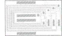
图8a描绘了图7b的分层半导体器件的俯视图和平面图。在此图和下面的图中,描绘致使形成两组存储元件和相关联的字线、屏蔽板和触点的衬底的区域。每组存储元件包括八条字线和九个屏蔽板。另外,在区域802和804中提供源极选择栅极,而在区域800和806中提供漏极选择栅极。具体地,构图后的光刻胶部分801被示出为横跨存储器阵列延伸以形成闭环。在一些存储器阵列中,可使用若干类似的同心环。除了后面用于提供字线和屏蔽板触点的各种开口之外,还类似地在光刻胶部分801之间形成同心开口。Figure 8a depicts top and plan views of the layered semiconductor device of Figure 7b. In this figure and the figures below, regions of the substrate that result in the formation of two sets of storage elements and associated word lines, shielding plates and contacts are depicted. Each set of memory elements includes eight word lines and nine shielding plates. Additionally, source select gates are provided in
图8b描绘了在进行光刻胶瘦化后的图7c的分层半导体器件的俯视图。如所述,这带来了变窄的(narrowed)光刻胶部分810。Figure 8b depicts a top view of the layered semiconductor device of Figure 7c after photoresist thinning. This results in a narrowed photoresist portion 810 as described.
图8c描绘了SiN蚀刻和光刻胶剥除后的图7d的分层半导体器件的俯视图。在此步骤中,基于光刻胶层来构图SiN层,并移除光刻胶层。Figure 8c depicts a top view of the layered semiconductor device of Figure 7d after SiN etch and photoresist stripping. In this step, the SiN layer is patterned based on the photoresist layer, and the photoresist layer is removed.
图8d描绘了图7f的分层半导体器件的俯视图。在分层结构上进行SiO2沉积,并且在用于形成字线和屏蔽板触点的区域中提供光刻胶掩模,如示例掩模810。Figure 8d depicts a top view of the layered semiconductor device of Figure 7f.SiO2 deposition is performed on the layered structure and a photoresist mask, such as example mask 810, is provided in the areas used to form wordlines and shield plate contacts.
图8e描绘了图7g的分层半导体器件的俯视图。进行SiO2蚀刻和光刻胶剥除,留下SiN部分和SiO2侧壁隔板。Figure 8e depicts a top view of the layered semiconductor device of Figure 7g. ASiO2 etch and photoresist strip is performed, leaving the SiN part and theSiO2 sidewall spacers.
图8f描绘了图7h的分层半导体器件的俯视图。湿蚀刻移除SiN层的部分,由此留下SiO2侧壁隔板的部分。Figure 8f depicts a top view of the layered semiconductor device of Figure 7h. The wet etch removes portions of the SiN layer, thereby leaving portions of theSiO2 sidewall spacers.
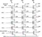
图8g描绘了从图8f的器件形成的分层半导体器件的俯视图,示出了由两组存储元件共享的字线触点和屏蔽板触点。在图7i-k所示的处理之后,字线和屏蔽板与它们的触点一起形成。在图中,“W”表示字线触点,而“S”表示屏蔽板触点。存在可根据期望的控制方案将不同电压分别耦接到字线或屏蔽板的触点。例如,第一组存储元件820包括在源极选择栅极824和漏极选择栅极822之间交替延伸的多个屏蔽板和字线。类似地,第二组存储元件822包括在源极选择栅极828和漏极选择栅极830之间交替延伸的多个屏蔽板和字线。字线由两组存储元件共享。例如,字线触点832耦接到WL0,其在穿过两组存储元件的电路中延伸。同样,字线触点834耦接到WL1,字线触点836耦接到WL2,字线触点838耦接到WL3,字线触点840耦接到WL4,字线触点842耦接到WL5,字线触点844耦接到WL6,并且字线触点846耦接到最后一条字线WL7。同样,提供八条字线仅仅作为例子。Figure 8g depicts a top view of a layered semiconductor device formed from the device of Figure 8f, showing word line contacts and shield plate contacts shared by two sets of memory elements. After the processing shown in Figures 7i-k, word lines and shield plates are formed with their contacts. In the figure, "W" indicates a word line contact, and "S" indicates a shield plate contact. There are contacts that can couple different voltages to the word lines or shield plates, respectively, depending on the desired control scheme. For example, the first set of
类似地,屏蔽板由两组存储元件共享。例如,屏蔽板触点850耦接到在穿过两组存储元件的电路中延伸的第一屏蔽板SP0。具体地,SP0在第一组存储元件820中的SGS 824和WL0之间,以及在第二组存储元件826中的SGS 828和WL0之间延伸。屏蔽板触点852耦接到在WL0和WL1之间延伸的SP1。屏蔽板触点854耦接到在WL1和WL2之间延伸的SP2。屏蔽板触点856耦接到在WL2和WL3之间延伸的SP3。屏蔽板触点858耦接到在WL3和WL4之间延伸的SP4。屏蔽板触点860耦接到在WL4和WL5之间延伸的SP5。屏蔽板触点862耦接到在WL5和WL6之间延伸的SP6。屏蔽板触点864耦接到在WL6和WL7之间延伸的SP7。屏蔽板触点866耦接到在第一组存储元件820中的WL7和SGD 822以及在第二组存储元件826的WL7和SGD 830之间延伸的SP8。Similarly, the shield plate is shared by two sets of storage elements. For example, shield contact 850 is coupled to a first shield SP0 that extends in a circuit through two sets of memory elements. Specifically, SP0 extends between SGS 824 and WL0 in the first set of
在该配置中,可将电压独立耦接到在两组存储元件820和826之间共享的给定字线或屏蔽板。可使用合适的控制电路来将期望的电压耦接到触点。In this configuration, voltages can be coupled independently to a given word line or shield shared between the two sets of
注意,所示的布置仅仅是示例,其他布置也是可能的。例如,可在存储元件组820和826的左侧或右侧布置一个或更多附加的存储元件组。在此情况下,在图中水平延伸的字线可进一步水平延伸跨越附加的存储元件组。另外,例如,可在图中字线垂直延伸的区域中提供一个或更多组存储元件。Note that the arrangements shown are examples only and other arrangements are possible. For example, one or more additional storage element groups may be arranged to the left or right of
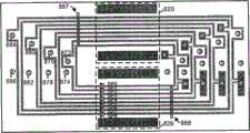
图8h描绘了替代分层半导体器件的俯视图,示出了用于每组存储元件的共享的字线触点和分离的屏蔽板触点。与图8g的配置相比,在存储元件组820和826与结合图8g讨论的触点所在的一侧相对的一侧上,添加附加的屏蔽板触点872-886。可使用类似于前面所述的光平版印刷技术来建立这些附加的屏蔽板触点。具体地,这些附加的屏蔽板触点耦接到延伸穿过第二组存储元件826但由于隔离结构887和888而不穿过第一组存储元件的屏蔽板。可使用本领域技术人员应清楚的技术由介电材料形成这些隔离结构,以使得屏蔽板短路,从而在第一组存储元件820中延伸并且耦接到图的右手边上的触点的屏蔽板不与第二组存储元件826通信,并且在第二组存储元件826中延伸并且耦接到图的左手边上的触点的屏蔽板不与第一组存储元件820通信。Figure 8h depicts a top view of an alternative layered semiconductor device showing shared word line contacts and separate shield plate contacts for each set of storage elements. Compared to the configuration of Figure 8g, additional shield plate contacts 872-886 are added on the opposite side of the
具体地,在图的左手边,屏蔽板触点872耦接到SP1,屏蔽板触点874耦接到SP2,屏蔽板触点876耦接到SP3,屏蔽板触点878耦接到SP4,屏蔽板触点880耦接到SP5,屏蔽板触点882耦接到SP6,屏蔽板触点884耦接到SP7,并且屏蔽板触点886耦接到SP8。注意,在一种方式中,屏蔽板触点850(见图8g)可用于两组存储元件。还可以提供分离的屏蔽板触点,它们耦接到在第一组存储元件820中的SGS 824和WL0之间的以及在第二组存储元件826的SGS 828和WL0之间的分离的屏蔽板。在此情况下,使用合适的绝缘结构将屏蔽板彼此绝缘。Specifically, on the left hand side of the figure, shield contact 872 is coupled to SP1,
在该配置中,能将电压独立地耦接到两组存储元件之间共享的给定字线以及与给定存储元件组相关联的给定屏蔽板。如前,可使用合适的控制电路将期望的电压耦接到触点。In this configuration, voltages can be independently coupled to a given word line shared between two sets of storage elements and to a given shield associated with a given set of storage elements. As before, suitable control circuitry can be used to couple the desired voltage to the contacts.
图8i描绘了替代分层半导体器件的俯视图,示出了用于每组存储元件的分离的字线触点和屏蔽板触点。与图8h的配置相比,在存储元件组820和826的左侧添加附加的字线触点890-897。可使用类似于前面所述的光平版印刷技术建立这些附加的字线触点。具体地,这些附加的字线触点耦接到延伸穿过第二组存储元件826但由于隔离结构898和899而不穿过第一组存储元件的字线。可使用本领域技术人员应清楚的技术由介电材料形成这些隔离结构,以使得字线短路,从而在第一组存储元件820中延伸并且耦接到图的右手边上的触点的字线不与第二组存储元件826通信,并且在第二组存储元件826中延伸并且耦接到图的左手边上的触点的字线不与第一组存储元件820通信。Figure 8i depicts a top view of an alternative layered semiconductor device showing separate word line contacts and shield plate contacts for each set of storage elements. Compared to the configuration of Figure 8h, additional word line contacts 890-897 are added to the left of
具体地,在图的左手边,字线触点890耦接到WL0,字线触点891耦接到WL1,字线触点892耦接到WL2,字线触点893耦接到WL3,字线触点894耦接到WL4,字线触点895耦接到WL5,字线触点896耦接到WL6,并且字线触点897耦接到WL7。Specifically, on the left hand side of the figure, word line contact 890 is coupled to WL0, word line contact 891 is coupled to WL1, word line contact 892 is coupled to WL2, word line contact 893 is coupled to WL3, word line Line contact 894 is coupled to WL4, word line contact 895 is coupled to WL5, word line contact 896 is coupled to WL6, and word line contact 897 is coupled to WL7.
在该配置中,能将电压独立地耦接到与给定存储元件组相关联的给定字线以及与给定存储元件组相关联的给定屏蔽板。如前,可使用合适的控制电路将期望的电压耦接到触点。In this configuration, voltages can be independently coupled to a given word line associated with a given group of storage elements and a given shield associated with a given group of storage elements. As before, suitable control circuitry can be used to couple the desired voltage to the contacts.
图9描绘了阵列中的存储元件的四个块或其他组,其中由一对块共享字线和屏蔽板。这里,描绘了四个块900、910、920和930作为例子,但可使用附加的块的对。另外,可在共同的p阱上提供块。在一个可能的配置中,块n和n+1共享字线和屏蔽板,块n+2和n+3共享字线和屏蔽板。作为例示,提供八条字线WL0至WL7和九个屏蔽板SP0至SP8。用块的右手边上的实线描绘字线,而用虚线描绘屏蔽板。还对每个块描绘了漏极选择栅极(SGD)和源极选择栅极(SGS)。在一种方式中,每对块共享行/字线解码和屏蔽板解码,因为字线和屏蔽板是共享的,而每个块具有其自己的选择栅极源极和漏极解码。Figure 9 depicts four blocks or other groups of storage elements in an array, where word lines and shielding plates are shared by a pair of blocks. Here, four blocks 900, 910, 920, and 930 are depicted as an example, but additional pairs of blocks may be used. Alternatively, blocks can be provided on a common p-well. In one possible configuration, blocks n and n+1 share word lines and shields, and blocks n+2 and n+3 share word lines and shields. As an illustration, eight word lines WL0 to WL7 and nine shield plates SP0 to SP8 are provided. The word lines are depicted with solid lines on the right-hand side of the block, while the shield plates are depicted with dashed lines. A drain select gate (SGD) and a source select gate (SGS) are also depicted for each block. In one approach, each pair of blocks shares the row/wordline decode and shield decode since the wordline and shield are shared, while each block has its own select gate source and drain decode.
图10描绘了用于制造具有屏蔽板的非易失性存储装置的工艺。步骤1000包括形成例如图7a所示的分层结构。步骤1005包括施加(apply)光刻胶和构图(pattern)光刻胶(见图7b)。步骤1010包括光刻胶瘦化(见图7c)。步骤1015包括SiN蚀刻和光刻胶剥除(见图7d)。步骤1020包括SiO2沉积(见图7e)。步骤1025包括施加用于选择栅极的光刻胶掩模(见图7f)。步骤1030包括进行SiO2蚀刻和光刻胶剥除(见图7g)。步骤1035包括SiN湿蚀刻(见图7h)。步骤1040包括执行用于字线的上面的多晶硅层的多晶硅蚀刻(见图7i)。步骤1045包括蚀刻用于浮置栅极的O-N-O层和下面的多晶硅层(见图7j)。步骤1050包括沉积和研磨(polish)多晶硅层以提供屏蔽板(见图7k)。FIG. 10 depicts a process for fabricating a non-volatile memory device with a shield plate. Step 1000 includes forming a layered structure such as that shown in Figure 7a. Step 1005 includes applying and patterning photoresist (see Figure 7b). Step 1010 includes photoresist thinning (see Figure 7c). Step 1015 includes SiN etching and photoresist stripping (see Figure 7d). Step 1020 includesSiO2 deposition (see Figure 7e). Step 1025 includes applying a photoresist mask for the select gates (see Figure 7f). Step 1030 includes performingSiO2 etching and photoresist stripping (see FIG. 7g). Step 1035 includes a SiN wet etch (see Figure 7h). Step 1040 includes performing a polysilicon etch of the overlying polysilicon layer for the wordlines (see Figure 7i). Step 1045 includes etching the ONO layer for the floating gate and the underlying polysilicon layer (see Figure 7j). Step 1050 includes depositing and polishing a polysilicon layer to provide a shield (see Figure 7k).
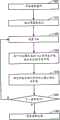
图11是描述用于对非易失性存储器编程的方法的一个实施例的流程图。在一个实现方式中,在编程之前(以块或其他单位)擦除存储元件。在步骤1100中,由控制电路(circuitry)发出“数据加载”命令。在步骤1105中,指定页地址的地址数据被从控制器或主机输入到解码器。在步骤1110中,用于所寻址的页的编程数据的页被输入到数据缓冲器以用于编程。该数据被锁存在合适的锁存器组中。在步骤1115中,发出“编程”命令。Figure 11 is a flowchart describing one embodiment of a method for programming non-volatile memory. In one implementation, storage elements are erased (in blocks or other units) prior to programming. In
由“编程”命令触发,将使用被施加到合适的所选字线的图12的脉冲串1200的步进的(stepped)编程脉冲1205、1210、1215、1220、1225、1230、1235、1240、1245、1250...,而把在步骤1110中锁存的数据编程到所选存储元件中。在步骤1120中,编程电压VPGM被初始化为起始脉冲(例如,13V或其他值),并且编程计数器(PC)被初始化为零。在步骤1125中,根据期望的编程控制方案(见再下面的例子)施加用于编程的屏蔽板电压。在步骤1130中,第一VPGM脉冲被施加到所选字线以开始编程与所选字线相关联的存储元件。如果逻辑“0”被存储在特定数据锁存器中,表示相应的存储元件应该被编程,则相应的位线被接地。另一方面,如果逻辑“1”被存储在特定锁存器中,表示相应的存储元件应该保留其当前状态,则相应的位线连接到Vdd,大约2V的内部调节电压,以禁止编程。Triggered by the "program" command, the stepped
在步骤1135中,根据期望的感测控制方案(见再下面的例子)施加屏蔽板电压。在步骤1140中,校验所选存储元件的状态。如果检测到所选存储元件的目标阈值电压已经达到合适的电平,则把所存储在相应数据锁存器中的数据变为逻辑“1”。如果检测到阈值电压还未达到合适的电平,则存储在相应数据锁存器中的数据不改变。以此方式,在其相应数据锁存器中存储了逻辑“1”的位线不需要被编程。当所有的数据锁存器存储逻辑“1”时,所有的所选存储元件已经被编程。在步骤1145中(校验状态),检查是否所有的数据锁存器都存储逻辑“1”。如果所有的数据锁存器都存储逻辑“1”,则编程处理完成并成功,因为所有的所选存储元件都被编程和校验。在步骤1150中报告状态“通过”。In
如果在步骤1145中确定不是所有的数据存储器都存储逻辑“1”,则编程处理继续。在步骤1155中,针对编程限制值PCmax检查编程计数器PC。编程限制值的一个例子是二十;然而,也可使用其他数字。如果编程计数器PC不比PCmax小,则编程过程已经失败,并且在步骤1160中报告状态“失败”。如果编程计数器比PCmax小,则在步骤1165中按步长增加VPGM并且编程计数器PC递增,并且处理循环回到步骤1125。If in
图12描绘了在编程期间施加到非易失性存储元件的控制栅极的示例脉冲串1200。脉冲串1200包括一系列编程脉冲1205、1210、1215、1220、1225、1230、1235、1240、1245、1250...,其被施加到所选择进行编程的字线。在一个实施例中,编程脉冲具有电压VPGM,其从13V开始并对于每个连续编程脉冲按例如0.5V的增量增加,直到达到最大21V。在编程脉冲之间的是校验脉冲。例如,校验脉冲组1206包括三个校验脉冲。在一些实施例中,对于正将数据编程到其的每个状态,例如状态A、B和C,可存在校验脉冲。在其他实施例中,可以有更多或更少的校验脉冲。FIG. 12 depicts an example pulse train 1200 applied to the control gates of non-volatile storage elements during programming. Pulse train 1200 includes a series of
图13是描述用于读取非易失性存储器的处理的一个实施例的流程图。读取处理从步骤1300开始。在步骤1310中,根据期望的控制方案施加用于感测的屏蔽板电压。在步骤1320,例如,基于最高读取电平设置VCGR。步骤1330包括根据控制方案将VCGR施加到所选字线并将电压施加到未选字线。在步骤1340,确定所选存储元件何时从截止转变为导通。如果在判定步骤1350存在下一读取电平,则过程以不同的VCGR从步骤1320继续。如果没有下一读取电平,则在步骤1360,读取处理结束。Figure 13 is a flowchart describing one embodiment of a process for reading non-volatile memory. Read processing begins at
下面提供示例控制方案作为例示。控制方案应用于由两个块的存储元件共享字线和屏蔽板的情况。然而,控制方案也可用于单个块或其他组的存储元件。其他控制方案也是可能的。A sample control scheme is provided below as an illustration. The control scheme applies to the case where word lines and shield plates are shared by memory elements of two blocks. However, the control scheme can also be used for individual blocks or other groups of storage elements. Other control schemes are also possible.
表1描绘了对于不使用源极/漏极植入(implant)的实施例,在例如读取或校验操作的感测操作期间可以使用的电压。还参图见6。在该表格和其他表格中,对块n+1进行操作,其中块n和n+1共享字线和屏蔽板。然而,用于对块n进行操作的电压是类似的。具体地,所示施加到块n+1的SGD和SGS的电压将被施加到块n,并且所示施加到块n的SGD和SGS的电压将被施加到块n+1。类似地,用于对块n+2或n+3进行操作的电压是类似的。此外,通过使用所提供的电压控制非共享的字线组和/或屏蔽板组,控制方案可适用于与不在存储元件组之间共享的字线和/或屏蔽板一起使用。Table 1 depicts voltages that may be used during sensing operations such as read or verify operations for embodiments that do not use source/drain implants. See also Figure 6. In this and other tables, operations are performed on block n+1, where block n and n+1 share word lines and shield plates. However, the voltages used to operate block n are similar. Specifically, the voltages shown applied to SGD and SGS of block n+1 will be applied to block n, and the voltages shown applied to SGD and SGS of block n will be applied to block n+1. Similarly, the voltages used to operate block n+2 or n+3 are similar. In addition, by using the provided voltages to control non-shared word line groups and/or shield groups, the control scheme can be adapted for use with word lines and/or shield groups that are not shared between storage element groups.
描绘了施加到漏极选择栅极(SGD)、字线、源极选择栅极(SGS)、阵列源极和p阱的电压。在示例实现方式中,VREAD(施加到未选字线的读取流通电压)是大约4.5V,VRSPH(读取、屏蔽板、高电压)是大约4V,VRSPL(读取、屏蔽板、低电压)是大约2V,并且VSS(稳定状态电压)是大约0V。注意,在一种可能的方式中,VRSPL可以是VRSPH的大约30至90%。另外,VRSPH可以是VREAD的大约50至150%。VCGR(控制栅极读取电压)被施加到所选字线,并且对于与不同编程状态或状况相关联的不同比较电平而改变。VCGR在不同时间被设置于不同电平,以确定何时所选存储元件在导通/截止状态之间转变。值“i”表示字线的数目,并且从NAND串的源极侧处的WL0到NAND串的漏极侧处的WLi-1对字线进行编号。从WL0的源极侧处的SP0到WLi-1的漏极侧处的SPi对屏蔽板进行编号。The voltages applied to the drain select gate (SGD), word line, source select gate (SGS), array source and p-well are depicted. In an example implementation, VREAD (read pass-through voltage applied to unselected word lines) is approximately 4.5V, VRSPH (read, shield plate, high voltage) is approximately 4V, VRSPL (read, shield plate, low voltage ) is about 2V, and VSS (steady state voltage) is about 0V. Note that VRSPL may be approximately 30 to 90% of VRSPH in one possible approach. Additionally, VRSPH may be approximately 50 to 150% of VREAD. VCGR (Control Gate Read Voltage) is applied to the selected word line and varies for different compare levels associated with different programming states or conditions. VCGR is set at different levels at different times to determine when selected storage elements transition between on/off states. The value "i" represents the number of word lines, and the word lines are numbered from WL0 at the source side of the NAND string to WLi-1 at the drain side of the NAND string. The shield plates are numbered from SP0 at the source side of WL0 to SPi at the drain side of WLi-1.
VREAD被施加到未选字线,而VCGR被施加到所选字线。另外,VRSPL被施加到与所选字线相邻的屏蔽板。具体地,VRSPL被施加到位于WLn的源极侧上的SPn,并施加到位于WLn的漏极侧上的SPn+1。其余屏蔽板交替接收VRSPH和VRSPL,例如,SPn+2上的VRSPH、SPn+3上的VRSPL、SPn+4上的VRSPH等,以及SPn-1上的VRSPH、SPn-2上的VRSPL、SPn-3上的VRSPH等。此外,对于其他块的对,在与块n和n+1的相同p阱上形成的块n+2和n+3,在字线和屏蔽板上浮置电压。VREAD is applied to unselected word lines, and VCGR is applied to selected word lines. In addition, VRSPL is applied to the shield plate adjacent to the selected word line. Specifically, VRSPL is applied to SPn on the source side of WLn, and to SPn+1 on the drain side of WLn. The remaining shields receive VRSPH and VRSPL alternately, for example, VRSPH on SPn+2, VRSPL on SPn+3, VRSPH on SPn+4, etc., and VRSPH on SPn-1, VRSPL on SPn-2, SPn- VRSPH on 3, etc. Also, for the other pair of blocks, blocks n+2 and n+3 formed on the same p-well as blocks n and n+1, the voltage is floated on the word line and the shield plate.


表2描绘了表1的控制方案的替代例,并且可用于针对具有或不具有源极-漏极植入的情况进行感测。这里,使用单个屏蔽板电压VRSP而不是分别地高和低屏蔽板电压VRSPH和VRSPL。在示例实现方式中,VRSP是大约4-5V。例如,VRSP可以是VREAD的大约50至150%。VSS(0V)被施加到与所选字线相邻的屏蔽板。具体地,VSS被施加到位于WLn的源极侧上的SPn,并施加到位于WLn的漏极侧上的SPn+1。其余屏蔽板交替接收VSS和VRSP,例如,SPn+2上的VRSP、SPn+3上的VSS、SPn+4上的VRSP等,以及SPn-1上的VRSP、SPn-2上的VSS、SPn-3上的VRSP等。Table 2 depicts an alternative to the control scheme of Table 1 and can be used for sensing with or without source-drain implants. Here, a single shield plate voltage VRSP is used instead of high and low shield plate voltages VRSPH and VRSPL, respectively. In an example implementation, VRSP is approximately 4-5V. For example, VRSP may be approximately 50 to 150% of VREAD. VSS (0V) is applied to the shield adjacent to the selected word line. Specifically, VSS is applied to SPn on the source side of WLn, and to SPn+1 on the drain side of WLn. The remaining shield boards receive VSS and VRSP alternately, for example, VRSP on SPn+2, VSS on SPn+3, VRSP on SPn+4, etc., and VRSP on SPn-1, VSS on SPn-2, SPn- VRSP on 3 etc.

表3描绘了可在自升压(self-boosting)模式下具有或不具有源极-漏极植入的实施例的编程操作期间使用的电压。在示例实现方式中,VPASS(施加到未选字线的流通电压)是大约9V,VPSPH(编程、屏蔽板、高电压)是大约9V,VPSPL(编程、屏蔽板、低电压)是大约6V,并且VDD(内部稳定(regulated)电压)是大约2V。VTH是漏极选择栅极的阈值电压并且可以是大约0.7-1.2V。注意,在一种可能的方式中,VPSPL可以是VPSPH的大约50至90%。另外,VPSPH可以是VPGM的大约50至100%。VPGM(编程电压)被施加到所选字线,并且一般按逐步(step wise)方式从大约13V增加到21V。见图12。Table 3 depicts voltages that can be used during a programming operation of embodiments in self-boosting mode with or without source-drain implants. In an example implementation, VPASS (pass voltage applied to unselected word lines) is approximately 9V, VPSPH (program, shield plate, high voltage) is approximately 9V, VPSPL (program, shield plate, low voltage) is approximately 6V, And VDD (internal regulated voltage) is about 2V. VTH is the threshold voltage of the drain select gate and may be about 0.7-1.2V. Note that in one possible approach, VPSPL may be approximately 50 to 90% of VPSPH. Additionally, VPSPH can be approximately 50 to 100% of VPGM. VPGM (Program Voltage) is applied to the selected word line and is typically increased from about 13V to 21V in a step wise manner. See Figure 12.
VPASS被施加到未选字线,而VPGM被施加到所选字线。另外,VPSPH被施加到与所选字线相邻的屏蔽板。具体地,VRSPH被施加到位于WLn的源极侧上的SPn,并施加到位于WLn的漏极侧上的SPn+1。其余未选的屏蔽板交替接收VPSPH和VPSPL,例如,SPn+2上的VPSPL、SPn+3上的VPSPH、SPn+4上的VPSPL等,以及SPn-1上的VPSPL、SPn-2上的VPSPH、SPn-3上的VPSPL等。此外,对于块n+2和n+3,在字线和屏蔽板上浮置电压。VPASS is applied to unselected word lines, and VPGM is applied to selected word lines. In addition, VPSPH is applied to the shield plate adjacent to the selected word line. Specifically, VRSPH is applied to SPn on the source side of WLn and to SPn+1 on the drain side of WLn. The remaining unselected shields receive VPSPH and VPSPL alternately, for example, VPSPL on SPn+2, VPSPH on SPn+3, VPSPL on SPn+4, etc., and VPSPL on SPn-1, VPSPH on SPn-2 , VPSPL on SPn-3, etc. Also, for blocks n+2 and n+3, the voltage is floated on the word line and the shield plate.

表格4描绘了可能在擦除区域自升压模式(EASB)下不具有源极-漏极植入的实施例的编程操作期间使用的电压。在示例实现方式中,VPASS是大约9V,VPSPH是大约10V,VPSPL是大约6V,并且VDD是大约2V。VPASS被施加到除了接收VDD的WLn-1和接收0V的WLn-2之外的未选字线。VPGM被施加到所选字线。另外,VPSPH被施加到与所选字线相邻的屏蔽板。具体地,VRSPH被施加到位于WLn的源极侧上的SPn,并施加到位于WLn的漏极侧上的SPn+1。除了接收VDD的SPn-1和SPn-2之外,其余屏蔽板交替接收VPSPH和VPSPL。例如,控制提供SPn+2上的VPSPL、SPn+3上的VPSPH、SPn+4上的VPSPL等,以及SPn-3上的VPSPH、SPn-4上的VPSPL、SPn-5上的VPSPH等。此外,对于块n+2和n+3,在字线和屏蔽板上浮置电压。Table 4 depicts voltages that may be used during a programming operation for an embodiment without source-drain implants in erased area self boosting mode (EASB). In an example implementation, VPASS is about 9V, VPSPH is about 10V, VPSPL is about 6V, and VDD is about 2V. VPASS is applied to unselected word lines except WLn-1 receiving VDD and WLn-2 receiving 0V. VPGM is applied to the selected word line. In addition, VPSPH is applied to the shield plate adjacent to the selected word line. Specifically, VRSPH is applied to SPn on the source side of WLn and to SPn+1 on the drain side of WLn. Except for SPn-1 and SPn-2 which receive VDD, the remaining shield boards receive VPSPH and VPSPL alternately. For example, the control provides VPSPL on SPn+2, VPSPH on SPn+3, VPSPL on SPn+4, etc., and VPSPH on SPn-3, VPSPL on SPn-4, VPSPH on SPn-5, etc. Also, for blocks n+2 and n+3, the voltage is floated on the word line and the shield plate.
为对包括源极-漏极植入的存储器器件编程,在EASB模式下,可使用表4的控制方案,除了在指定屏蔽板和字线上VSS替代VDD。For programming memory devices that include source-drain implants, in EASB mode, the control scheme of Table 4 can be used, except VSS is substituted for VDD on designated shields and word lines.

表格5描绘了可能在局部自升压模式(LSB)下不具有源极-漏极植入的实施例的编程操作期间使用的电压。在示例实现方式中,VPASS是大约9V,VPSPH是大约10V,VPSPL是大约6V,并且VDD是大约2V。VPASS被施加到除了接收VDD的WLn-1和WLn+1以及接收0V的WLn-2和WLn+2之外的未选字线。VPGM被施加到所选字线。另外,VPSPH被施加到与所选字线相邻的屏蔽板。具体地,VRSPH被施加到位于WLn的源极侧上的SPn,并施加到位于WLn的漏极侧上的SPn+1。除了接收VDD的SPn-1、SPn-2、SPn+1和SPn+2之外,其余未选屏蔽板交替接收VPSPH和VPSPL。例如,控制提供SPn+4上的VPSPH、SPn+5上的VPSPL、SPn+6上的VPSPH等,以及SPn-3上的VPSPH、SPn-4上的VPSPL、SPn-5上的VPSPH等。此外,对于块n+2和n+3,在字线和屏蔽板上浮置电压。Table 5 depicts voltages that may be used during a program operation for an embodiment without source-drain implants in local self-boost mode (LSB). In an example implementation, VPASS is about 9V, VPSPH is about 10V, VPSPL is about 6V, and VDD is about 2V. VPASS is applied to unselected word lines except WLn-1 and WLn+1 receiving VDD and WLn-2 and WLn+2 receiving 0V. VPGM is applied to the selected word line. In addition, VPSPH is applied to the shield plate adjacent to the selected word line. Specifically, VRSPH is applied to SPn on the source side of WLn and to SPn+1 on the drain side of WLn. Except for SPn-1, SPn-2, SPn+1 and SPn+2 which receive VDD, the remaining unselected shields receive VPSPH and VPSPL alternately. For example, the control provides VPSPH on SPn+4, VPSPL on SPn+5, VPSPH on SPn+6, etc., and VPSPH on SPn-3, VPSPL on SPn-4, VPSPH on SPn-5, etc. Also, for blocks n+2 and n+3, the voltage is floated on the word line and the shield plate.
为编程包括源极-漏极植入的存储器器件,在LSB模式下,可使用表5的控制方案,除了在指定屏蔽板和字线上VSS替代VDD。For programming memory devices that include source-drain implants, in LSB mode, the control scheme of Table 5 can be used, except VSS is substituted for VDD on designated shields and word lines.


表格6描绘了具有或不具有源极-漏极植入的实施例的擦除操作期间使用的电压。在示例实现方式中,VERASE(擦除电压)是大约20V。该相对高的电压被施加到p阱,而VSS被施加到正被擦除的块例如块n和n+1的字线和屏蔽板,以移除在存储元件的浮置栅极中存储的电荷。对于块n+2和n+3,在字线和屏蔽板上浮置电压。Table 6 depicts the voltages used during erase operations for embodiments with and without source-drain implants. In an example implementation, VERASE (erase voltage) is approximately 20V. This relatively high voltage is applied to the p-well, while VSS is applied to the word line and shield plate of the block being erased, such as blocks n and n+1, to remove the memory stored in the floating gate of the storage element. charge. For blocks n+2 and n+3, the voltage is floated on the word line and the shield plate.
已经为了例示和描述的目的给出了本发明的前述详细说明。不意图它是穷尽的或将本发明限于所公开的精确形式。根据以上教导,许多修改和变化是可能的。选择了所描述的实施例以便最好地解释本发明的原理及其实践应用,从而使得本领域技术人员在各种实施例中并使用适合于预期特定用途的各种修改来最好地利用本发明。希望由所附权利要求限定本发明的范围。The foregoing detailed description of the invention has been presented for purposes of illustration and description. It is not intended to be exhaustive or to limit the invention to the precise forms disclosed. Many modifications and variations are possible in light of the above teaching. The described embodiment was chosen in order to best explain the principles of the invention and its practical application, to enable others skilled in the art to best utilize the invention in various embodiments and with various modifications as are suited to the particular use contemplated. invention. It is intended that the scope of the invention be defined by the appended claims.
Claims (20)
Applications Claiming Priority (7)
| Application Number | Priority Date | Filing Date | Title |
|---|---|---|---|
| US11/767,647US7636260B2 (en) | 2007-06-25 | 2007-06-25 | Method for operating non-volatile storage with individually controllable shield plates between storage elements |
| US11/767,647 | 2007-06-25 | ||
| US11/767,661 | 2007-06-25 | ||
| US11/767,652 | 2007-06-25 | ||
| US11/767,661US7781286B2 (en) | 2007-06-25 | 2007-06-25 | Method for fabricating non-volatile storage with individually controllable shield plates between storage elements |
| US11/767,652US7808826B2 (en) | 2007-06-25 | 2007-06-25 | Non-volatile storage with individually controllable shield plates between storage elements |
| PCT/US2008/068048WO2009002983A1 (en) | 2007-06-25 | 2008-06-24 | Non-volatile storage with individually controllable shield plates between storage elements |
Publications (2)
| Publication Number | Publication Date |
|---|---|
| CN101711413A CN101711413A (en) | 2010-05-19 |
| CN101711413Btrue CN101711413B (en) | 2013-09-04 |
Family
ID=40186016
Family Applications (1)
| Application Number | Title | Priority Date | Filing Date |
|---|---|---|---|
| CN200880021966.6AActiveCN101711413B (en) | 2007-06-25 | 2008-06-24 | Non-volatile memory device with individually controllable shielding plates between memory elements |
Country Status (4)
| Country | Link |
|---|---|
| KR (1) | KR101373794B1 (en) |
| CN (1) | CN101711413B (en) |
| TW (1) | TWI387976B (en) |
| WO (1) | WO2009002983A1 (en) |
Families Citing this family (3)
| Publication number | Priority date | Publication date | Assignee | Title |
|---|---|---|---|---|
| DK2411395T3 (en)* | 2009-03-23 | 2013-08-05 | Glenmark Pharmaceuticals Sa | Furopyrimidine dione derivatives as modulators of TRPA1 |
| US8432740B2 (en)* | 2011-07-21 | 2013-04-30 | Sandisk Technologies Inc. | Program algorithm with staircase waveform decomposed into multiple passes |
| CN111403415B (en) | 2018-06-29 | 2021-05-25 | 长江存储科技有限责任公司 | Three-dimensional memory device with shielding layer and method of forming the same |
Citations (3)
| Publication number | Priority date | Publication date | Assignee | Title |
|---|---|---|---|---|
| CN1427468A (en)* | 2001-12-18 | 2003-07-02 | 旺宏电子股份有限公司 | Method of making non-volatile memory element |
| TW200616236A (en)* | 2004-03-12 | 2006-05-16 | Sandisk Corp | Self aligned non-volatile memory cells and processes for fabrication |
| TWI273685B (en)* | 2005-12-13 | 2007-02-11 | Macronix Int Co Ltd | Non-volatile memory package and method of reading stored data from a non-volatile memory array |
Family Cites Families (3)
| Publication number | Priority date | Publication date | Assignee | Title |
|---|---|---|---|---|
| US7355237B2 (en)* | 2004-02-13 | 2008-04-08 | Sandisk Corporation | Shield plate for limiting cross coupling between floating gates |
| US7655536B2 (en) | 2005-12-21 | 2010-02-02 | Sandisk Corporation | Methods of forming flash devices with shared word lines |
| US7495294B2 (en)* | 2005-12-21 | 2009-02-24 | Sandisk Corporation | Flash devices with shared word lines |
- 2008
- 2008-06-24WOPCT/US2008/068048patent/WO2009002983A1/enactiveApplication Filing
- 2008-06-24KRKR1020107001712Apatent/KR101373794B1/ennot_activeExpired - Fee Related
- 2008-06-24CNCN200880021966.6Apatent/CN101711413B/enactiveActive
- 2008-06-25TWTW097123797Apatent/TWI387976B/ennot_activeIP Right Cessation
Patent Citations (3)
| Publication number | Priority date | Publication date | Assignee | Title |
|---|---|---|---|---|
| CN1427468A (en)* | 2001-12-18 | 2003-07-02 | 旺宏电子股份有限公司 | Method of making non-volatile memory element |
| TW200616236A (en)* | 2004-03-12 | 2006-05-16 | Sandisk Corp | Self aligned non-volatile memory cells and processes for fabrication |
| TWI273685B (en)* | 2005-12-13 | 2007-02-11 | Macronix Int Co Ltd | Non-volatile memory package and method of reading stored data from a non-volatile memory array |
Also Published As
| Publication number | Publication date |
|---|---|
| KR20100050483A (en) | 2010-05-13 |
| TWI387976B (en) | 2013-03-01 |
| TW200912955A (en) | 2009-03-16 |
| KR101373794B1 (en) | 2014-03-13 |
| WO2009002983A1 (en) | 2008-12-31 |
| CN101711413A (en) | 2010-05-19 |
Similar Documents
| Publication | Publication Date | Title |
|---|---|---|
| US7800947B2 (en) | Multiple select gates with non-volatile memory cells | |
| KR101099803B1 (en) | Semiconductor device including contact plug having an elliptical sectional shape | |
| US7923767B2 (en) | Non-volatile storage with substrate cut-out and process of fabricating | |
| US9047971B2 (en) | Operation for non-volatile storage system with shared bit lines | |
| US8837216B2 (en) | Non-volatile storage system with shared bit lines connected to a single selection device | |
| JP2000269366A (en) | Non-volatile semiconductor memory | |
| US20220254382A1 (en) | Buried source line structure for boosting read scheme | |
| US7808826B2 (en) | Non-volatile storage with individually controllable shield plates between storage elements | |
| US8062944B2 (en) | Method for fabricating non-volatile storage with individually controllable shield plates between storage elements | |
| US7636260B2 (en) | Method for operating non-volatile storage with individually controllable shield plates between storage elements | |
| US20070166918A1 (en) | Non-volatile memory device, and manufacturing method and programming method thereof | |
| CN101711413B (en) | Non-volatile memory device with individually controllable shielding plates between memory elements | |
| WO2014189808A2 (en) | Inverted-t word line and formation for non-volatile storage | |
| JP2010515271A (en) | Shield plate manufacturing method for reducing field coupling in non-volatile memory | |
| US9349452B2 (en) | Hybrid non-volatile memory cells for shared bit line | |
| US20130028028A1 (en) | Nonvolatile semiconductor memory device | |
| JP2011192898A (en) | Semiconductor memory device, and method of manufacturing the same | |
| JP4864097B2 (en) | Flash memory device with booster plate | |
| JP2011018755A (en) | Nonvolatile semiconductor storage device and method of manufacturing the same |
Legal Events
| Date | Code | Title | Description |
|---|---|---|---|
| C06 | Publication | ||
| PB01 | Publication | ||
| C10 | Entry into substantive examination | ||
| SE01 | Entry into force of request for substantive examination | ||
| ASS | Succession or assignment of patent right | Owner name:SANDISK CORPORATION Free format text:FORMER OWNER: SANDISK CORP. Effective date:20120625 | |
| C41 | Transfer of patent application or patent right or utility model | ||
| TA01 | Transfer of patent application right | Effective date of registration:20120625 Address after:Texas, USA Applicant after:SANDISK TECHNOLOGIES Inc. Address before:California, USA Applicant before:Sandisk Corp. | |
| C14 | Grant of patent or utility model | ||
| GR01 | Patent grant | ||
| C56 | Change in the name or address of the patentee | ||
| CP01 | Change in the name or title of a patent holder | Address after:Texas, USA Patentee after:SANDISK TECHNOLOGIES LLC Address before:Texas, USA Patentee before:SANDISK TECHNOLOGIES Inc. | |
| TR01 | Transfer of patent right | ||
| TR01 | Transfer of patent right | Effective date of registration:20250328 Address after:U.S.A. Patentee after:SANDISK TECHNOLOGIES Inc. Country or region after:U.S.A. Address before:texas Patentee before:SANDISK TECHNOLOGIES LLC Country or region before:U.S.A. |