CN101710890A - Pulse and OFDMD double-data modulation method - Google Patents
Pulse and OFDMD double-data modulation methodDownload PDFInfo
- Publication number
- CN101710890A CN101710890ACN200910201114ACN200910201114ACN101710890ACN 101710890 ACN101710890 ACN 101710890ACN 200910201114 ACN200910201114 ACN 200910201114ACN 200910201114 ACN200910201114 ACN 200910201114ACN 101710890 ACN101710890 ACN 101710890A
- Authority
- CN
- China
- Prior art keywords
- modulation
- ofdm
- pulse
- signal
- data
- Prior art date
- Legal status (The legal status is an assumption and is not a legal conclusion. Google has not performed a legal analysis and makes no representation as to the accuracy of the status listed.)
- Granted
Links
Images


Landscapes
- Optical Communication System (AREA)
Abstract
Translated fromChineseDescription
Translated fromChinese技术领域technical field
本发明属于通信技术领域,具体涉及的是利用照明LED实现短距通信时的一种脉冲和OFDM的双重数据调制和解调的装置及方法。The invention belongs to the technical field of communication, and specifically relates to a device and method for dual data modulation and demodulation of pulse and OFDM when using lighting LEDs to realize short-distance communication.
背景技术Background technique
基于照明LED的可见光通信是一种新兴的短距无线通信方式,有望取代或者补充当前的短距RF无线通信技术,以提高通信速率、降低成本和环境的电磁辐射。目前,已经初步证实了不同环境下使用照明用LED通信的可行性,其中包括在室内和智能交通中的应用。Visible light communication based on lighting LED is an emerging short-range wireless communication method, which is expected to replace or supplement the current short-range RF wireless communication technology to improve communication speed, reduce cost and environmental electromagnetic radiation. At present, the feasibility of using LED communication for lighting in different environments has been initially confirmed, including applications in indoor and intelligent transportation.
通信的重要技术方面之一是对通信数据信号的调制。针对不同通信体制和应用需求,广义地讲,采用的调制方式有各种脉冲调制(PM)、QAM(正交幅度调制)调制、OFDM(正交频分复用)调制以及CDMA(码分多址)等。有效的调制方式对通信系统的数据传输速率、容量和质量有很大的影响。One of the important technical aspects of communication is the modulation of the communication data signal. According to different communication systems and application requirements, broadly speaking, the modulation methods used include various pulse modulation (PM), QAM (quadrature amplitude modulation) modulation, OFDM (orthogonal frequency division multiplexing) modulation and CDMA (code division multiplexing) modulation. address), etc. The effective modulation method has a great influence on the data transmission rate, capacity and quality of the communication system.
脉冲调制是一种比较简的调制方式,在有线的基带通信系统中常用,其中一种就是OOK(开关键控)调制。OFDM调制是一种有效消除信道多径延迟影响的多载波调制方式,其应用有越来越广泛的趋势,已经成功应用在xDSL(数字用户线)宽带接入系统和无线局域网标准IEEE802.11a中,并有可能应用在未来的多种无线通信系统。Pulse modulation is a relatively simple modulation method, commonly used in wired baseband communication systems, one of which is OOK (on-off keying) modulation. OFDM modulation is a multi-carrier modulation method that effectively eliminates the influence of channel multipath delay. Its application has become more and more extensive. It has been successfully applied in xDSL (Digital Subscriber Line) broadband access system and wireless local area network standard IEEE802.11a , and may be applied in a variety of wireless communication systems in the future.
可见光的波段在400nm到700nm之间,用作照明的大功率白光LED将是未来实现可见光通信的主体。常规的白光LED有两类:单芯片和多芯片,这是两种不同的实现技术。单芯片技术采用一个单色波段的LED激励黄色或者红色和绿色混合的荧光粉发出混合色的光,常用的激励光源是蓝光LED(或者紫外LED)。因此,单芯片白光LED的光谱特性截然分为冷色的蓝光和红黄色的暖色光两部分。在图1中示出了一个典型的单芯片白光LED的光谱曲线,作为激励光源的蓝光光谱大约在420nm-460nm范围,荧光粉发光的暖色光光谱大约在500nm-750nm范围。多芯片的白光LED由三基色光的LED构成。目前,由于照明时的功率需求,大多数白光LED采用单芯片的结构,而多芯片结构的白光LED多用于功率要求不太高但色彩质量要求较高的场合,如显示屏等。The wavelength band of visible light is between 400nm and 700nm, and the high-power white LED used for lighting will be the main body to realize visible light communication in the future. There are two types of conventional white LEDs: single-chip and multi-chip, which are two different implementation technologies. Single-chip technology uses a single-color band LED to excite yellow or red and green phosphors to emit mixed-color light. The commonly used excitation light source is blue LED (or ultraviolet LED). Therefore, the spectral characteristics of single-chip white LEDs are clearly divided into two parts: cool blue light and red-yellow warm light. Figure 1 shows the spectral curve of a typical single-chip white LED. The blue light spectrum as the excitation light source is in the range of 420nm-460nm, and the warm-color light spectrum emitted by the phosphor is in the range of 500nm-750nm. Multi-chip white LEDs are composed of LEDs with three primary colors. At present, due to the power requirements during lighting, most white light LEDs adopt a single-chip structure, while white light LEDs with a multi-chip structure are mostly used in occasions that require less power but higher color quality, such as display screens.
上述模式的单芯片LED,蓝光属于半导体性质,是直接电驱动,所以响应比较快,有很高的带宽。而荧光粉属于二次响应,速度较慢,带宽较窄。因此,当用LED进行通信时,存在一个不同光谱的光在响应速度上的差异。For the single-chip LED of the above mode, the blue light belongs to the nature of the semiconductor and is directly driven by electricity, so the response is relatively fast and the bandwidth is very high. The phosphor belongs to the secondary response, which is slower and has a narrower bandwidth. Therefore, when LEDs are used for communication, there is a difference in response speed for different spectrums of light.
目前对可见光通信的研究,采用的调制方式有OOK方式、PWM方式、CDMA方式(如Tim C.W.Schenk,“Optical Wireless CDMA Employing Solid StateLighting LEDs”)、OFDM方式(如Hany Elgala,“Indoor Broadcasting via White LEDsand OFDM”)等。鉴于可见光照明LED发射光的非相干性和单极性,通常认为OOK方式可能是实现比较简单又能够达到一定速率的较实用的调制方式,而OFDM则是比较复杂但能够在非相干波上实现多载波高速传输的调制形式。The current research on visible light communication adopts OOK, PWM, CDMA (such as Tim C.W.Schenk, "Optical Wireless CDMA Employing Solid State Lighting LEDs"), OFDM (such as Hany Elgala, "Indoor Broadcasting via White LEDs and OFDM") and so on. In view of the incoherence and unipolarity of the light emitted by visible light illumination LEDs, it is generally believed that the OOK method may be a relatively simple and practical modulation method that can achieve a certain rate, while OFDM is more complicated but can be realized on incoherent waves. Modulation form for multi-carrier high-speed transmission.
如果只用一个光接收机接收全光谱频段的光,那么通信系统的带宽决定于慢响应的暖色光。目前大多数的研究,针对就是这一种情况,系统能够实现的带宽大概在10MHz左右。另外也有研究单独针对蓝色光部分的快速响应特性,如在Hoa Le Minh的论文“100-Mb/s NRZ Visible Light Communications Using aPostequalized White LED”和S.C.J.Lee的论文“Discrete Multitone for NovelApplication Areas of Optical Communications”中,采用了蓝色滤光片滤除掉了慢速暖色光,从而在简单的OOK调制下或者在OFDM调制下达到了很高的数据传输速率。但是,这种方法显然无法用到蓝色光之外的大部分光的能量,而这部分光在采用OFDM调制时,也能够达到大约同样量级的数据传输速率。If only one optical receiver is used to receive light in the full spectrum frequency band, then the bandwidth of the communication system is determined by the slow response of warm light. At present, most of the research is aimed at this kind of situation, and the bandwidth that the system can realize is about 10MHz. In addition, there are also studies on the fast response characteristics of the blue light part alone, such as Hoa Le Minh's paper "100-Mb/s NRZ Visible Light Communications Using a Postequalized White LED" and S.C.J. Lee's paper "Discrete Multitone for Novel Application Areas of Optical Communications" In , a blue filter is used to filter out the slow warm light, thus achieving a high data transmission rate under simple OOK modulation or OFDM modulation. However, this method obviously cannot use most of the energy of light other than blue light, and this part of light can also achieve data transmission rates of about the same order of magnitude when modulated with OFDM.
如果在光发射机端,能够单独控制不同光谱的光,那么在接收机端用滤光片就能够分出不同光谱的信号,从而实现多路通信。对多芯片白光LED,如R、G、B三色LED封装在一起的白光LED,如果能够单独控制,就是一种可能实现3路并行通信的方法。但是对于通常的单芯片白光LED,只能够对激励光(通常是蓝光)进行控制,通过激励光的强度大小获取相应的暖色光强度(这种比例由LED的内部特定的配色组成决定),两者实际上是密切相关的,无法独立使用。If the light of different spectra can be controlled separately at the optical transmitter end, then the signals of different spectra can be separated by using optical filters at the receiver end, thereby realizing multi-channel communication. For multi-chip white light LEDs, such as R, G, and B three-color LEDs packaged together, if they can be controlled separately, it is a possible way to achieve 3-way parallel communication. But for the usual single-chip white light LED, only the excitation light (usually blue light) can be controlled, and the corresponding warm color light intensity can be obtained through the intensity of the excitation light (this ratio is determined by the internal specific color composition of the LED), two The latter are actually closely related and cannot be used independently.
针对上述问题,本专利提出了一种实现蓝光脉冲调制的同时实现暖色光OFDM调制的“PM-OFDM”双路高速传输数据方法。In view of the above problems, this patent proposes a "PM-OFDM" two-way high-speed data transmission method that realizes blue light pulse modulation and warm-color light OFDM modulation at the same time.
发明内容Contents of the invention
本发明的初始目的是充分利用白光LED的光谱特性和响应特性,实现一种基于白光LED的高速数据调制和解调。The original purpose of the present invention is to make full use of the spectral characteristics and response characteristics of white light LEDs to realize a high-speed data modulation and demodulation based on white light LEDs.
本发明的基本思路是:以蓝光为LED激励源时,在激励脉冲序列的时间维度上进行一种脉冲调制,在其幅度上进行匹配于暖色光OFDM波形的调制,由此实现两路数据信息在不同光谱上的并行传输。The basic idea of the present invention is: when blue light is used as the LED excitation source, a pulse modulation is performed on the time dimension of the excitation pulse sequence, and a modulation matching the OFDM waveform of the warm color light is performed on its amplitude, thereby realizing two-way data information Parallel transmissions on different spectra.
在光发射机端,发送数据流被分为两路:DPM(n)和DOFDM(n)。At the optical transmitter side, the transmitted data stream is divided into two paths: DPM (n) and DOFDM (n).
数据流DPM(n)经过常规的编码、交织、扰码等基带通信系统常用的预处理措施后,对时钟频率为ΦP的脉冲序列进行OOK脉冲调制,形成携带数据信息的等幅调制脉冲序列PPM(n),假定有脉冲代表数据“1”、无脉冲代表数据“0”,脉冲的幅度为1。这个脉冲序列作为信号同时送到两个地方,一个是激励补偿单元,一个是控制LED电流通断的开关电路。激励补偿单元的作用是判断当前调制脉冲PPM(n)之后的调制脉冲PPM(n-1)是否为零。如果为零,则在当前的脉冲幅度1上增加一个Δ后输出,否则维持原幅度1输出。这个新脉冲序列具有同样的频率ΦP,但不再是等幅脉冲,记为PΔPM(n)。PΔPM(n)被送到调制器MOOK-OFDM的第一个输入端口。送到LED通断控制的调制脉冲PPM(n),延迟Td后,当PPM(n)=1时,打开LED,当PPM(n)=0时,关闭LED。打开LED即允许LED发送光信号,关闭LED即不允许LED发送光信号。而所允许发送的光信号的大小决定于施加在LED上的偏置电压VLED。After the data stream DPM (n) undergoes conventional preprocessing measures such as conventional encoding, interleaving, and scrambling in baseband communication systems, OOK pulse modulation is performed on the pulse sequence with a clock frequency of ΦP to form an equal-amplitude modulation pulse carrying data information In the sequence PPM (n), it is assumed that there is a pulse representing data "1", and no pulse represents data "0", and the amplitude of the pulse is 1. This pulse sequence is sent to two places as a signal at the same time, one is the excitation compensation unit, and the other is the switch circuit that controls the LED current on and off. The function of the excitation compensation unit is to judge whether the modulation pulse PPM (n-1) after the current modulation pulse PPM (n) is zero. If it is zero, add a Δ to the
数据流DOFDM(n)经过常规的编码、交织、QAM调制、导频插入、映射、IFFT变换等OFDM通信系统常用的处理措施后,形成取样频率为ΦOFDM的时域离散OFDM实信号。时钟频率ΦP与ΦOFDM为整数倍关系。将样点频率为ΦOFDM的离散OFDM信号按照频率ΦP进行插值运算,得到一个取样频率为ΦP的离散OFDM信号SOFDM(n)。将这个离散信号进行一个预偏置Vb转换为单极性信号,送到调制器MOOK-OFDM的第二个输入端口。调制器的输出信号就是幅度被OFDM信号调制且补偿过的频率为ΦP的脉冲序列SΔOFDM(n)。这个脉冲序列然后被送到一个DAC转换器,转换为模拟信号并被功率放大后成为LED的正向偏置电压(工作电压)VLED。After the data stream DOFDM (n) undergoes common processing measures in OFDM communication systems such as conventional coding, interleaving, QAM modulation, pilot insertion, mapping, and IFFT transformation, it forms a time-domain discrete OFDM real signal with a sampling frequency of ΦOFDM . The clock frequency ΦP and ΦOFDM are integer multiples. The discrete OFDM signal with a sampling frequency of ΦOFDM is interpolated according to the frequency ΦP to obtain a discrete OFDM signal SOFDM (n) with a sampling frequency of ΦP. This discrete signal is converted into a unipolar signal by a pre-bias Vb and sent to the second input port of the modulatorMOOK-OFDM . The output signal of the modulator is the pulse sequence SΔOFDM (n) whose amplitude is modulated by the OFDM signal and the compensated frequency is ΦP. This pulse train is then sent to a DAC converter, converted to an analog signal and amplified by the power to become the forward bias voltage (operating voltage) VLED of the LED.
白光LED受两个信号的同步作用:一个是施加在其上的工作电压,其大小反映了信号SΔOFDM(n)大小,决定LED导通时的电流;一个是控制LED电流通断的脉冲调制信号PPM(n)。共同作用的结果是LED输出的光信号,在蓝光波段由于其快速响应特性,输出的光信号反映了脉冲调制信号PPM(n),在时间轴上隐含发送的OOK调制数据信息和时钟信息,幅度轴上隐含发送的OFDM数据调制信息;在暖光波段由于荧光粉较大的响应时常数脉冲信息被平滑掉,因而仅隐含了OFDM波形数据信息。The white light LED is synchronized by two signals: one is the working voltage applied to it, and its magnitude reflects the signal SΔOFDM (n), which determines the current when the LED is turned on; the other is the pulse modulation that controls the LED current on and off Signal PPM (n). The result of the combined effect is the optical signal output by the LED. Due to its fast response characteristics in the blue light band, the output optical signal reflects the pulse modulation signal PPM (n), and the OOK modulated data information and clock information are implicitly sent on the time axis , the modulation information of OFDM data transmitted is implied on the amplitude axis; in the warm light band, due to the large response time constant pulse information of the phosphor is smoothed out, only the OFDM waveform data information is implied.
在光接收机端,有两个光接收通道:一个是蓝光接收通道,一个是暖光接收通道。On the optical receiver side, there are two optical receiving channels: one is the blue light receiving channel, and the other is the warm light receiving channel.
蓝光接收通道首先经过蓝光滤光片,滤除掉蓝光之外的光能量。进入接收机的蓝光进行光电转换、放大、滤波等处理后,信号被送往两个数据处理通道:脉冲处理通道和OFDM处理通道。脉冲处理通道直接对输入的脉冲信号进行处理,得到脉冲的同步信息、直流偏置电平并解调出调制的数据。OFDM处理通道首先将脉冲信号进行包络检波,得到脉冲信号幅度的轮廓信息。这个信息在发射机端实际上就是OFDM信号,对这个信号再进行ADC变换,得到离散的OFDM信号,记为SB-OFDM(k),然后去掉直流偏置转换为双极性信号送到一个合并器MRC。The blue light receiving channel first passes through a blue light filter to filter out light energy other than blue light. After the blue light entering the receiver is processed by photoelectric conversion, amplification, filtering, etc., the signal is sent to two data processing channels: pulse processing channel and OFDM processing channel. The pulse processing channel directly processes the input pulse signal, obtains pulse synchronization information, DC bias level and demodulates modulated data. The OFDM processing channel first performs envelope detection on the pulse signal to obtain the contour information of the pulse signal amplitude. This information is actually an OFDM signal at the transmitter end. ADC conversion is performed on this signal to obtain a discrete OFDM signal, which is denoted as SB-OFDM (k), and then the DC bias is removed and converted into a bipolar signal and sent to a Combiner MRC.
暖光接收通道首先经过暖光滤光片,滤除掉暖光之外的光能量。然后,对进入接收机的暖光进行光电转换、放大、滤波等处理后,在同步信号的同步下对信号进行ADC变换,得到离散的OFDM信号,记为SW-OFDM(k),然后去掉直流偏置转换为双极性信号也送到合并器MRC。合并器MRC选择一定的加权算法,比如比值合并算法将两路OFDM信号同步地合并为一路OFDM信号,然后去掉循环前缀,进行FFT变换、去映射、QAM解调、去交织、解码,得到OFDM调制数据。The warm light receiving channel first passes through the warm light filter to filter out light energy other than warm light. Then, after performing photoelectric conversion, amplification, and filtering on the warm light entering the receiver, the signal is converted by ADC under the synchronization of the synchronous signal to obtain a discrete OFDM signal, which is denoted asSW-OFDM (k), and then removed The DC bias is converted into a bipolar signal and sent to the combiner MRC. The combiner MRC selects a certain weighting algorithm, such as the ratio combining algorithm to synchronously combine two OFDM signals into one OFDM signal, then remove the cyclic prefix, perform FFT transformation, demapping, QAM demodulation, deinterleaving, and decoding to obtain OFDM modulation data.
上述方法,可以看作是基于OOK脉冲载波的OFDM调制(当用PWM调制时,可以称为基于PWM脉冲载波的OFDM调制)。针对单芯片的白光LED,双重调制的结果是能够实现两路光发送通道:蓝光脉冲光通道和暖光连续波通道,而所用的LED仍旧只需要一个(或一组,但控制端口只需要一个)。在接收机端利用两个光接收通道,能够得到三路数据信息:一路独立的脉冲调制数据,两路关联的OFDM调制数据。这种方法除了增加数据传输速率外,同时获得了频率(蓝光、暖色光)分集增益。这种收发机可以灵活配置,根据信道状况和传输质量要求,将三个通道传输同样的数据或者只选用某一个通道都是容易实现的。The above method can be regarded as OFDM modulation based on OOK pulse carrier (when PWM modulation is used, it can be called OFDM modulation based on PWM pulse carrier). For single-chip white LEDs, the result of dual modulation is that two optical transmission channels can be realized: blue light pulsed light channel and warm light continuous wave channel, and the LED used still only needs one (or a group, but the control port only needs one ). Using two optical receiving channels at the receiver end, three channels of data information can be obtained: one channel of independent pulse modulation data and two channels of associated OFDM modulation data. In addition to increasing the data transmission rate, this method also obtains frequency (blue light, warm light) diversity gain. This kind of transceiver can be flexibly configured. According to the channel conditions and transmission quality requirements, it is easy to transmit the same data through three channels or only select a certain channel.
附图说明Description of drawings
图1:典型的单芯片白光LED光谱图。Figure 1: Spectral diagram of a typical single-chip white LED.
图2:可见光通信场景示意。Figure 2: Schematic diagram of visible light communication scenarios.
图3:LED实现可见光通信的收发机组成。Figure 3: Transceiver composition of LEDs for visible light communication.
图4:OOK和PWM调制的脉冲信号。Figure 4: OOK and PWM modulated pulse signal.
图5:采用OFDM调制的可见光通信系统。Figure 5: Visible light communication system using OFDM modulation.
图6:以脉冲为载波的OFDM调制过程和输出波形。Figure 6: OFDM modulation process and output waveform with pulse as carrier.
图7:OOK-OFDM双重调制过程和对应的输出波形。Figure 7: OOK-OFDM dual modulation process and corresponding output waveforms.
图8:采用双重调制的可见光通信系统的收发机组成。Figure 8: Transceiver composition of a visible light communication system using dual modulation.
图9:接收的OOK调制信号的检测门限。Figure 9: Detection threshold of received OOK modulated signal.
图10:OOK脉冲调制通道的同步信号之一种,采用了双脉冲巴克码。Figure 10: One of the synchronization signals of the OOK pulse modulation channel, using a double-pulse Barker code.
图11:三通道的OOK-OFDM双重调制光收发机系统实现框图。Figure 11: A block diagram of a three-channel OOK-OFDM dual modulation optical transceiver system.
图12:OOK-OFDM双重调制及其激励补偿的实现。Figure 12: Implementation of OOK-OFDM dual modulation and its excitation compensation.
图13:脉冲激励补偿示意图。Figure 13: Schematic diagram of pulse excitation compensation.
图14:双光学通道接收前端。Figure 14: Dual optical channel receive front end.
具体实施方式Detailed ways
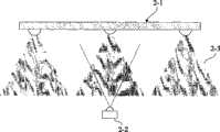
利用照明LED实现通信的场景一般如图2所示,单个的或者成阵列、成簇的LED(2-1)以各种形式实现需要的照明,同时成为光发射机。最通常的是安装在室内的房顶上,做成台灯放置在桌子上,或者安装在汽车、飞机的座位上方等。而光接收机(2-2)通常位于照明LED的下方。不同于RF无线传播,照明光一般存在一定的方向性(2-3),特别是采用LED时,光照的范围比较容易控制。这种方向性在一定程度上对实现多址/多路通信有利。The scenario of using lighting LEDs to realize communication is generally shown in FIG. 2 , where single or arrayed or clustered LEDs (2-1) realize required lighting in various forms and become light transmitters at the same time. The most common is to be installed on the roof of the room, made into a desk lamp and placed on the table, or installed above the seats of cars and airplanes. And the light receiver (2-2) is usually located below the lighting LED. Different from RF wireless transmission, illumination light generally has a certain directionality (2-3), especially when LED is used, the range of illumination is relatively easy to control. This directionality is beneficial to achieve multiple access/multiple communication to a certain extent.
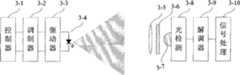
可见光通信系统的收发机一般构成如图3所示。发射机由控制器(3-1)、调制器(3-2)、驱动器(3-3)和发光二极管(3-4)构成,接收机由简单的透镜(3-5)、滤光片(3-6)构成的光学系统、光电转换器(3-7)、信号检测电路(3-8)、信号解调电路(3-9)、信号处理器(3-10)构成。除了电-光、光-电转换部分取代RF无线通信的射频单元外,其总的通信组成与RF通信相同。The general structure of the transceiver of the visible light communication system is shown in Fig. 3 . The transmitter consists of a controller (3-1), a modulator (3-2), a driver (3-3) and a light-emitting diode (3-4), and the receiver consists of a simple lens (3-5), optical filter (3-6) constitutes an optical system, a photoelectric converter (3-7), a signal detection circuit (3-8), a signal demodulation circuit (3-9), and a signal processor (3-10). Except that the radio frequency unit of RF wireless communication is partially replaced by electric-optical and optical-electrical conversion, its overall communication composition is the same as that of RF communication.
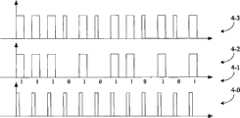
可见光通信的调制方式需要适合于非相干的单极性信号,常用的是开关键控(OOK)调制、脉冲宽度(PWM)调制等。在图4中示出了二进制的OOK和PWM调制方式。在时钟脉冲(4-0)的触发下,数据序列(4-1)按照OOK调制转换为信号(4-2)的脉冲形式,同样的数据序列按照PWM调制转换为(4-3)的脉冲形式。The modulation method of visible light communication needs to be suitable for incoherent unipolar signals, commonly used are on-off keying (OOK) modulation, pulse width (PWM) modulation, etc. The binary OOK and PWM modulation modes are shown in FIG. 4 . Under the trigger of the clock pulse (4-0), the data sequence (4-1) is converted into the pulse form of the signal (4-2) according to the OOK modulation, and the same data sequence is converted into the pulse form of (4-3) according to the PWM modulation form.
可见光OFDM调制通过将频带划分成多个并行的正交子频带,不但具有常规无线通信系统采用OFDM时所具有的优点,同时间接实现了非相干光信号无法实现的正交调制,如QPSK。在图5中所示出了OFDM调制的主要组成及数据操作流向。Visible light OFDM modulation divides the frequency band into multiple parallel orthogonal sub-bands, which not only has the advantages of conventional wireless communication systems using OFDM, but also indirectly realizes the orthogonal modulation that cannot be achieved by incoherent optical signals, such as QPSK. Figure 5 shows the main components of OFDM modulation and the flow of data operations.
发送端的原始数据流首先经过信道编码器(5-1)进行必要的纠错编码,然后经过交织器(5-2)对编码数据流进行交织,以提高对突发干扰的纠错能力。交织后的数据被调制器(5-3)转换成对应QPSK星座图的一组调制数据,然后按照子频带的数量转换成并行的对称复共轭数据并与导频信号(5-4b)一起由(5-4a)映射到规定的子频带上。并行的相当于频域的数据输入到傅里叶反变换器IFFT(5-5)转换成时域的一个实离散信号。按照系统设计时所针对的光信道的延时大小,CP插入模块(5-6)在此信号的尾部提取部分信号样点作为循环前缀(CP)插入到信号的前部,形成一个完整的离散OFDM符号。离散OFDM符号经过数模转换器DAC(5-7)转换为连续的OFDM时域信号波形,施加直流偏置转换为单极性信号后再经过功率驱动器(5-8)驱动LED,最终将电信号转换为光强度信号发送到可见光信道(5-9)中。The original data stream at the sending end is firstly subjected to necessary error correction encoding by the channel encoder (5-1), and then interleaved by the interleaver (5-2) to improve the error correction capability for burst interference. The interleaved data is converted into a set of modulated data corresponding to the QPSK constellation diagram by the modulator (5-3), and then converted into parallel symmetric complex conjugate data according to the number of sub-bands and together with the pilot signal (5-4b) Mapped to the specified sub-band by (5-4a). Parallel data corresponding to the frequency domain is input to the inverse Fourier transformer IFFT (5-5) and converted into a real discrete signal in the time domain. According to the delay of the optical channel targeted for system design, the CP insertion module (5-6) extracts some signal samples from the tail of the signal as a cyclic prefix (CP) and inserts them into the front of the signal to form a complete discrete OFDM symbols. Discrete OFDM symbols are converted into continuous OFDM time-domain signal waveforms by digital-to-analog converter DAC (5-7), applied DC bias, converted into unipolar signals, and then driven by power drivers (5-8) to drive LEDs, and finally power The signal is converted into a light intensity signal and sent to the visible light channel (5-9).
在OFDM可见光接收机端,通过光信道(5-9)的光信号被光检测器(5-10)检测并转换为电信号,经过必要的放大和滤波(5-11),连续的信号经过ADC转换器(5-12)在OFDM符号同步信号(5-13)的触发下,转换为离散的信号。这个信号与发射机端时域的离散OFDM信号对应,经过(5-14)移除循环前缀CP并去掉直流偏置,送到快速傅里叶变换器FFT(5-15)变换回频域的对应各个子载波的一组信号,经(5-16)去映射后,解调器(5-17)分解QPSK转换为串行的比特流。然后再经去交织(5-18)、纠错解码(5-19),输出接收的实际数据流。At the OFDM visible light receiver end, the optical signal passing through the optical channel (5-9) is detected by the optical detector (5-10) and converted into an electrical signal, and after necessary amplification and filtering (5-11), the continuous signal passes through The ADC converter (5-12) is converted into a discrete signal under the trigger of the OFDM symbol synchronization signal (5-13). This signal corresponds to the discrete OFDM signal in the time domain of the transmitter. After (5-14) removing the cyclic prefix CP and removing the DC offset, it is sent to the fast Fourier transformer FFT (5-15) to transform back to the frequency domain A group of signals corresponding to each subcarrier is demapped by (5-16), and the demodulator (5-17) decomposes QPSK and converts it into a serial bit stream. Then go through deinterleaving (5-18), error correction decoding (5-19), and output the received actual data stream.
上述调制方式都是单一的基带调制,只能够传输一路数据。本发明提出的方法是同时利用脉冲和OFDM调制,实现双路数据传输。原理如下:The above modulation methods are all single baseband modulation, which can only transmit one channel of data. The method proposed by the invention uses pulse and OFDM modulation at the same time to realize two-way data transmission. The principle is as follows:
对于可见光通信,采用基带直接运行的OFDM系统传输的时域信号就是OFDM波形的光形式。而由于可见光的非相干性质,难以进行基于光波的载波调制,但是基于副载波(相对于光波)或者脉冲波的调制仍旧是可行的。在图6中示出了一种用脉冲波调制OFDM信号的实现过程。信号S(ofdm)假设是寄载了数据信息的OFDM信号波形(6-1),S(p)是脉冲载波(6-2),两个信号经过调制器(6-3)后,输出的波形S(p-ofdm)就是调制后的OFDM波形(6-4)。这个过程相当于一种幅度调制,输出脉冲信号的幅度包络完全记载了原始OFDM信号的波形信息。当然,这里的S(p)同样可以构造成正规的正弦波形式。For visible light communication, the time-domain signal transmitted by an OFDM system operating directly at the baseband is the optical form of the OFDM waveform. Carrier modulation based on light waves is difficult due to the incoherent nature of visible light, but modulation based on subcarriers (as opposed to light waves) or pulse waves is still feasible. Figure 6 shows a realization process of modulating OFDM signals with pulse waves. The signal S(ofdm) is assumed to be an OFDM signal waveform (6-1) carrying data information, and S(p) is a pulse carrier (6-2). After the two signals pass through the modulator (6-3), the output Waveform S(p-ofdm) is the modulated OFDM waveform (6-4). This process is equivalent to a kind of amplitude modulation, and the amplitude envelope of the output pulse signal completely records the waveform information of the original OFDM signal. Of course, S(p) here can also be constructed as a regular sine wave.
这种常规效果的调制方法,在脉冲载波中并不包含数据信息,输出波形(7-4)隐含的信息是一维的,它能够带来的只是传输系统频谱的改变和性能的改善。在可见光LED通信系统中,它的实际输出效果不同于RF系统。在蓝光波段,看到的将是如图6中所示S(p-ofdm)那样的脉冲波形(6-4),而在暖色光波段,看到的则是图6中S(led)那样的连续波形(6-5)。由于暖色光是由蓝光激励的,存在一个确定的响应关系和延迟(Td),因此当蓝光的脉冲激励频率比较高时,暖色光相当于将激励输入脉冲整流。The modulation method of this conventional effect does not contain data information in the pulse carrier, and the information implied by the output waveform (7-4) is one-dimensional, which can only bring about changes in the frequency spectrum and performance improvements of the transmission system. In the visible light LED communication system, its actual output effect is different from that of the RF system. In the blue light band, what you see will be the pulse waveform (6-4) like S(p-ofdm) shown in Figure 6, while in the warm light band, what you see will be like the S(led) in Figure 6 continuous waveform (6-5). Since warm-color light is excited by blue light, there is a definite response relationship and delay (Td ), so when the pulse excitation frequency of blue light is relatively high, warm-color light is equivalent to rectifying the excitation input pulse.
如此,当采用2个光波段的接收机时,在蓝光波段,能够同时获得脉冲载波的时间同步信息和OFDM调制的数据信息,而在暖色光波段能够获得具有更大能量的OFDM调制数据信息。双重的信息来源合并后相当于获取频率分集增益,使光接收机性能提高。而蓝光的独立接收获取的脉冲时间信息可以用来辅助暖色光的OFDM符号同步解调,这是一种有效的改善时间同步的措施。In this way, when two optical band receivers are used, in the blue light band, the time synchronization information of the pulse carrier and OFDM modulated data information can be obtained at the same time, while the OFDM modulated data information with greater energy can be obtained in the warm color light band. Combining the dual information sources is equivalent to obtaining frequency diversity gain, which improves the performance of the optical receiver. The pulse time information obtained by independent reception of blue light can be used to assist OFDM symbol synchronous demodulation of warm light, which is an effective measure to improve time synchronization.
当蓝光的时间响应很快时,另外一种增进数据传输能力的方法是,采用双重调制,即利用载波脉冲幅度信息寄载OFDM调制数据的同时,利用蓝光脉冲载波的时间信息记载另外一路数据。When the time response of Blu-ray is fast, another way to improve data transmission capability is to use dual modulation, that is, use the carrier pulse amplitude information to carry OFDM modulated data, and use the time information of the Blu-ray pulse carrier to record another channel of data.
在图7中示出了这种调制的过程。作为脉冲载波的信号S(ook)是确定时钟频率下连续脉冲波的OOK调制。图7中假设了一路数据(7-4),其对应的OOK调制输出波形是(7-3)。这个等幅的脉冲信号被送往调制器(7-5)作为调制载波。同时,另外一路数据流采用OFDM调制形成了OFDM波形(7-1),也送到调制器(7-5)。调制器的输出相当于脉冲信号的幅度和间隔被双重调制。The process of this modulation is shown in FIG. 7 . The signal S(ook) as a pulse carrier is OOK modulation of a continuous pulse wave at a certain clock frequency. Assuming one channel of data (7-4) in FIG. 7, the corresponding OOK modulation output waveform is (7-3). This equal-amplitude pulse signal is sent to the modulator (7-5) as a modulated carrier. At the same time, another data stream adopts OFDM modulation to form an OFDM waveform (7-1), which is also sent to the modulator (7-5). The output of the modulator is equivalent to the amplitude and interval of the pulse signal being double modulated.
在这个调制过程中,对OOK调制的数据首先进行扰码,使0、1比特出现概率相近,尽量避免出现连续的0比特位。这样0出现的影响减小,平均相当于调制脉冲的频率与脉冲时钟相比减少了一半。为保持输出光信号的平均强度,可以采用提高蓝光激励脉冲的平均幅度来补偿。In this modulation process, the OOK modulated data is first scrambled, so that the probability of occurrence of 0 and 1 bits is similar, and continuous 0 bits are avoided as much as possible. This reduces the effect of the appearance of 0, which on average corresponds to a reduction in half of the frequency of the modulating pulse compared to the pulse clock. In order to maintain the average intensity of the output optical signal, it can be compensated by increasing the average amplitude of the blue light excitation pulse.
由于暖色光的输出由蓝光的输出激励,为减少蓝色光脉冲不均匀激励影响暖色光输出的OFDM波形,另外采取一种逐脉冲补偿措施,补偿OOK调制的蓝光激励脉冲因出现比特0而缺位时暖色光的减弱,即在蓝光脉冲缺失时不使暖色光的激励强度受影响。Since the output of warm-color light is stimulated by the output of blue light, in order to reduce the uneven excitation of blue light pulses and affect the OFDM waveform of warm-color light output, a pulse-by-pulse compensation measure is adopted to compensate for the absence of OOK-modulated blue light excitation pulses due to the occurrence of
假设进入OOK调制的数据流和对应的脉冲串是:Assume that the data stream entering OOK modulation and the corresponding burst are:
D(0)、D(1)、...、D(n-1)、D(n)、D(n+1)、D(n+2)、D(n+3)...D(0), D(1),..., D(n-1), D(n), D(n+1), D(n+2), D(n+3)...
P(0)、P(1)、...、P(n-1)、P(n)、P(n+1)、P(n+2)、P(n+3)...P(0), P(1), ..., P(n-1), P(n), P(n+1), P(n+2), P(n+3)...
其中数据D(n)=0或者1,脉冲P(n)=0或者1(脉冲宽度固定时,指在幅度上为0或者1;幅度固定时,指宽度为T0或者T1(T0≠0,T1≠0,T0≠T1)。假定脉冲的频率在确定的时钟下不变)。在没有激励补偿时,OOK调制过程中:P(n)=D(n)。Wherein data D(n)=0 or 1, pulse P(n)=0 or 1 (when the pulse width is fixed, it means that it is 0 or 1 in the amplitude; when the amplitude is fixed, it means that the width is T0 or T1 (T0≠0, T1 ≠ 0, T0 ≠ T1). It is assumed that the frequency of the pulse does not change under a certain clock). When there is no excitation compensation, during OOK modulation: P(n)=D(n).
逐脉冲补偿的办法是在蓝光脉冲调制的OOK信号中,当发现存在D(n+k)=0时(k=0,1,...,K,使P(n-i)=1+Δi,(i=1,2,...,I;Δi≥0)。Δi的取值决定于LED中暖色荧光粉的响应特性和蓝光激励脉冲的能量,可以通过实验确定。在脉冲幅度上进行补偿相当于预先的PAM(脉冲幅度调制),而在脉冲的宽度上进行补偿相当于预先的PWM(脉冲宽度)调制。在图7中的信号S(ook-ofdm)就是逐脉冲幅度补偿(7-8)后的调制脉冲输出(7-6)。其中幅度超出OFDM调制波形(虚线示出)的脉冲幅度就是补偿的幅度,如图中标示出来的Δv1和Δv2。(7-6)就是蓝光的输出信号。在这样的信号激励下,产生的暖色光输出信号如图7中的S(led-ofdm)所示(7-7),它应该与输入的信号波形(7-1)相同,其中的Vb是直流偏置。The way of pulse-by-pulse compensation is in the OOK signal modulated by the blue light pulse, when it is found that there is D(n+k)=0 (k=0, 1, ..., K, so that P(n-i)=1+Δi, (i=1,2,...,I; Δi≥0).The value of Δi depends on the response characteristics of the warm-colored phosphor in the LED and the energy of the blue light excitation pulse, which can be determined by experiment.Compensate on the pulse amplitude Be equivalent to advance PAM (pulse amplitude modulation), and compensate on the width of pulse and be equivalent to advance PWM (pulse width) modulation.Signal S (ook-ofdm) among Fig. 7 is exactly pulse-by-pulse amplitude compensation (7- 8) After the modulated pulse output (7-6).Wherein the pulse amplitude exceeding the OFDM modulation waveform (shown in dotted line) is the amplitude of compensation, as shown in the figure, Δv1 and Δv2. (7-6) is exactly the blue light Output signal. Under such signal excitation, the warm color light output signal that produces is shown in (7-7) as (7-7) in S (led-ofdm) among Fig. 7, and it should be identical with the signal waveform (7-1) of input, wherein Vb is the DC bias.
可以用图8表示光收发机的构成。光发射机的控制器(8-1)将数据进行编码、交织、扰码等预处理后分成两路分别送到OOK调制器(8-2)和OFDM调制器(8-3),形成的信号送到驱动器(8-4)驱动LED(8-5)发出调制的光信号。在接收机端有两个接收通道,一个是蓝光接收通道,一个是暖色光接收通道。在蓝光接收通道,包含了两路调制数据的信息:OOK脉冲调制通道和OFDM调制通道。当光信号经过光学透镜(8-6)后,暖色光被滤光片(8-7)滤除,仅仅蓝色光被光电转换器(8-8)转换为电信号。其后在接收机(8-12)中分为两路。一路是脉冲信号的处理,滤波、检测、OOK解调等通常的通信脉冲信号处理,能够获得脉冲的同步信息和一路接收数据。另一路先对输入脉冲进行包络检波,然后进行OFDM信号的解调等处理,获得另一路数据,这一路数据和暖色光通道获得的数据是一个来源,因此可以进行联合检测。The configuration of the optical transceiver can be shown in FIG. 8 . The controller (8-1) of the optical transmitter divides the data into two channels after preprocessing such as encoding, interleaving, and scrambling, and sends them to the OOK modulator (8-2) and the OFDM modulator (8-3), forming a The signal is sent to the driver (8-4) to drive the LED (8-5) to send out the modulated light signal. There are two receiving channels at the receiver end, one is the blue light receiving channel, and the other is the warm color light receiving channel. In the Blu-ray receiving channel, two channels of modulation data information are included: OOK pulse modulation channel and OFDM modulation channel. After the optical signal passes through the optical lens (8-6), the warm-colored light is filtered by the filter (8-7), and only the blue light is converted into an electrical signal by the photoelectric converter (8-8). It is then divided into two paths in the receiver (8-12). One way is pulse signal processing, filtering, detection, OOK demodulation and other common communication pulse signal processing, which can obtain pulse synchronization information and one way receive data. The other channel first performs envelope detection on the input pulse, and then performs OFDM signal demodulation and other processing to obtain another channel of data. The data of this channel and the data obtained by the warm color light channel are from the same source, so joint detection can be performed.
在暖色光接收通道,当光信号经过光学透镜(8-9)后,蓝光被滤光片(8-10)滤除,仅仅暖色光被光电转换器(8-11)转换为电信号。其后,信号将在(8-12)中按照OFDM接收机的处理流程进行处理。蓝光接收通道获取的同步信息可以用来辅助此处OFDM符号的同步检测,数据的估计也可以和蓝光通道联合进行,减少误码率。In the warm-color light receiving channel, when the light signal passes through the optical lens (8-9), the blue light is filtered by the filter (8-10), and only the warm-color light is converted into an electrical signal by the photoelectric converter (8-11). Thereafter, the signal will be processed in (8-12) according to the processing flow of the OFDM receiver. The synchronization information obtained by the blue-ray receiving channel can be used to assist the synchronous detection of the OFDM symbols here, and the data estimation can also be performed jointly with the blue-ray channel to reduce the bit error rate.
两路含有同样数据信息的OFDM信号的联合检测的一种方法是在各路信号同步ADC转换后的离散信号进行加权合并,然后再进行OFDM的其余操作。假设蓝光通道ADC的输出Sb(n),暖色光通道ADC的输出是Sw(n),其中n是一个OFDM符号的离散采样点,那么联合输出为:One method of joint detection of two OFDM signals containing the same data information is to carry out weighted combination of discrete signals after synchronous ADC conversion of each signal, and then perform the rest of OFDM operations. Assuming that the output Sb (n) of the blue light channel ADC and the output of the warm color light channel ADC are Sw (n), where n is a discrete sampling point of an OFDM symbol, then the joint output is:
S∑(n)=Kb(n)×Sb(n)+Kw(n)×Sw(n) n=0,2,...,N-1S∑ (n) = Kb (n) × Sb (n) + Kw (n) × Sw (n) n = 0, 2, ..., N-1
其中,Kb(n)、Kw(n)分别为蓝光通道和暖光通道的加权系数,N为一个OFDM符号的样点数。加权系数的确定依据各信道的信噪比,采用最大比值合并是一种有效的方法。Among them, Kb (n) and Kw (n) are the weighting coefficients of the blue light channel and the warm light channel respectively, and N is the number of samples of one OFDM symbol. The determination of the weighting coefficient is based on the signal-to-noise ratio of each channel, and it is an effective method to use the maximum ratio combination.
获得S∑(n)后,按照OFDM的解调程序进行,去除CP循环前缀,送到FFT进行时域-频域变换得到数据端信号。After obtaining S∑ (n), follow the OFDM demodulation procedure, remove the CP cyclic prefix, and send it to FFT for time-frequency domain transformation to obtain the data terminal signal.
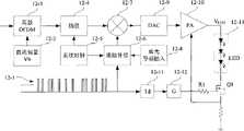
本发明实现所述的OOK脉冲载波OFDM调制的总体构成如图11所示。The overall composition of the present invention to realize the OOK pulse carrier OFDM modulation is shown in FIG. 11 .
光发射机端,被发送的数据流在(11-0)中分配为两路分别送到脉冲调制通道(11-1)和OFDM调制通道(11-2)。两个通道分别对所发送的数据进行调制,然后一起送到驱动器(11-3)驱动LED发出光信号到空间光信道(11-4)。在光接收机端有两个光接收通道,一个是蓝光接收通道(11-5),另一个是暖光接收通道(11-6)。蓝光接收通道主要完成对OOK脉冲调制信号的检测和解调,暖光接收通道主要完成对来自于蓝光和暖光的OFDM调制信号的联合检测和解调。三个数据通道一起完成输入信号的同步、信道估计和均衡(11-7)等处理。最后,两个接收通道的数据流在(11-8)合并成一个数据流输出。At the optical transmitter end, the transmitted data stream is divided into two paths in (11-0) and sent to the pulse modulation channel (11-1) and the OFDM modulation channel (11-2) respectively. The two channels respectively modulate the transmitted data, and then send them together to the driver (11-3) to drive the LED to send out light signals to the spatial optical channel (11-4). There are two light receiving channels at the optical receiver end, one is a blue light receiving channel (11-5), and the other is a warm light receiving channel (11-6). The blue light receiving channel mainly completes the detection and demodulation of the OOK pulse modulation signal, and the warm light receiving channel mainly completes the joint detection and demodulation of OFDM modulation signals from blue light and warm light. The three data channels together complete processing such as synchronization of the input signal, channel estimation and equalization (11-7). Finally, the data streams of the two receiving channels are combined into one data stream at (11-8) for output.
OFDM调制发送通道:信道编码(11-2-1)采用速率为R=2/3的卷积码,交织器的深度选为1024,数据在频域的调制(11-2-3)采用16-QAM,每4个比特构成一个数据符号,每60个数据符号补零和导频插入后形成64数据点(对应的子载波的数目为64个),经(11-2-4)共轭扩展映射到IFFT(11-2-5)的128个频域样点上。IFFT变换后,输出128个时域样点,再由(11-2-6)插入8个样点长度的CP(循环前缀)后构成一个离散的OFDM符号,然后经过OOK调制、DAC变换(11-2-7)到驱动器(11-3)激励LED发光。OFDM调制的总带宽设为8MHz,子带宽度为125KHz,信息符号的长度为8us,CP的长度为0.5us,长度足够适应任何环境下的多径延迟,总的OFDM符号长度为8.5us,取样速率ΦOFDM为16MHz。数据速率可以达到18.8Mbps。OFDM modulation transmission channel: channel coding (11-2-1) adopts a convolutional code with a rate of R=2/3, the depth of the interleaver is selected as 1024, and the modulation (11-2-3) of data in the frequency domain adopts 16 -QAM, every 4 bits constitute a data symbol, every 60 data symbols are filled with zeros and pilots are inserted to form 64 data points (the number of corresponding subcarriers is 64), via (11-2-4) conjugation The extension is mapped to 128 frequency domain samples of IFFT (11-2-5). After IFFT transformation, output 128 time-domain samples, and then insert CP (cyclic prefix) of 8 sample points length by (11-2-6) to form a discrete OFDM symbol, and then undergo OOK modulation and DAC conversion (11 -2-7) to the driver (11-3) to stimulate the LED to emit light. The total bandwidth of OFDM modulation is set to 8MHz, the sub-band width is 125KHz, the length of the information symbol is 8us, the length of the CP is 0.5us, the length is enough to adapt to the multipath delay in any environment, the total OFDM symbol length is 8.5us, sampling The rate ΦOFDM is 16MHz. The data rate can reach 18.8Mbps.
蓝光发送通道:脉冲载波的频率为48MHz,这也是系统的时钟频率ΦP,是OFDM取样频率的3倍,脉冲占空比取为50%。考虑到除了信道衰落影响传输数据的误码率外,还要受到OFDM调制的影响,选用信道编码(11-1-1)速率较低的R=1/2卷积码,交织器(11-1-2)的交织深度取为1024,扰码(11-1-3)选用伪随机序列。数据调制(11-1-4)采用OOK方式,比特“1”时脉冲“开”,比特“0”时脉冲“关”。不扩频时,数据速率能够达到近48Mbps,采用4倍扩频因子时(即用4位脉冲编码代表一位数据“1”或者“0”),数据速率能够达到12Mbps。如果采用PWM调制,如图4中由数据序列(4-1)调制后的脉冲序列(4-3),也可以达到同样的速率,不过后续的处理方式稍有不同。Blu-ray transmission channel: the pulse carrier frequency is 48MHz, which is also the system clock frequency ΦP , which is three times the OFDM sampling frequency, and the pulse duty cycle is 50%. Considering that in addition to channel fading affecting the bit error rate of the transmitted data, it is also affected by OFDM modulation, and the R=1/2 convolutional code with a lower rate of channel coding (11-1-1) is selected, and the interleaver (11-1-1) is selected. The interleaving depth of 1-2) is set to 1024, and the scrambling code (11-1-3) is selected as a pseudo-random sequence. The data modulation (11-1-4) adopts the OOK method, the pulse is "on" when the bit is "1", and the pulse is "off" when the bit is "0". When not spreading the spectrum, the data rate can reach nearly 48Mbps. When using 4 times the spreading factor (that is, using 4-bit pulse code to represent a bit of data "1" or "0"), the data rate can reach 12Mbps. If PWM modulation is used, as shown in Figure 4, the pulse sequence (4-3) modulated by the data sequence (4-1) can also achieve the same rate, but the subsequent processing method is slightly different.
蓝光接收通道接收的脉冲信号经过放大后整形(11-5-2)成矩形脉冲,一路送到(11-5-3)进行OOK解调、(11-5-4)去扰码/去交织、(11-5-5)解码等处理得到接收数据;另外一路送到包络检波器(11-6-3),检出其上调制的OFDM符号波形并去掉直流偏置。然后在(11-7)确定的同步信号下进行ADC(11-6-4)转换输出离散的OFDM样点。这个信号序列与来自于暖光通道的经过同步ADC(116-5)变换后的OFDM符号进行比值合并得到具有分集增益的和值序列,随后进行与OFDM发射系统对称的其它逆变换:循环前缀移除(11-6-8)、和发射通道IFFT点数相同的FFT(11-6-9)变换、反映射(11-6-10)、QAM解调(116-11)、去交织(11-6-12)、解码(11-6-13)。最后输出的数据与蓝光通道输出的数据在(11-8)中合并,形成最终的全部接收数据。The pulse signal received by the blue light receiving channel is amplified and shaped (11-5-2) into a rectangular pulse, and sent all the way to (11-5-3) for OOK demodulation, (11-5-4) descrambling/deinterleaving , (11-5-5) decoding and other processing to obtain the received data; the other path is sent to the envelope detector (11-6-3) to detect the OFDM symbol waveform modulated on it and remove the DC bias. Then ADC (11-6-4) conversion is performed under the synchronous signal determined by (11-7) to output discrete OFDM sample points. This signal sequence is combined with the OFDM symbols transformed by the synchronous ADC (116-5) from the warm light channel to obtain a sum sequence with diversity gain, followed by other inverse transformations symmetrical to the OFDM transmission system: cyclic prefix shift Divide (11-6-8), FFT (11-6-9) transformation with the same number of IFFT points as the transmit channel, reverse mapping (11-6-10), QAM demodulation (116-11), deinterleaving (11- 6-12), decoding (11-6-13). The finally output data and the data output by the Blu-ray channel are merged in (11-8) to form the final all received data.
发射机前端的双重调制实现方案之一是采用OOK调制后的等幅脉冲控制LED的通断,而LED的驱动电流的大小受补偿后的OFDM波形控制。在图12中示出了这种方案。(12-1)是OOK调制后的脉冲信号序列,已经包含了数据信息。它分成两路:一路送往激励补偿运算单元(12-6)计算每一个激励脉冲应该具有的幅度;另外一路经延迟单元(12-11)延迟一个时间Td后经门极驱动电路(12-12)输出驱动信号控制MOSFET开关管Q1的通断。延迟的时间Td保证OOK序列与OFDM通道输出的驱动信号中隐含的OOK序列同步。Q1具有良好的开关性能,能够快速打开/关断LED电流通道。连接在Q1和地之间的电阻R2是LED的限流和取样电阻,电流取样信号反馈到LED的驱动功率放大器(12-10)上,实现闭环电流调整。在OFDM调制通道,经过IFFT变换到时域的离散信号(12-3)被施加一个直流偏置Vb(12-2)转换为单极性信号后按照系统提供的时钟频率ΦP(12-5)经(12-4)插值后输出,插值后输出的样点频率与脉冲调制的时钟频率相同,插值的算法可以采用简单的线性插值方法。幅度补偿单元的功能是根据输入数据流中0的位置对前面的脉冲幅度进行调整,然后去调制(12-7)插值后的OFDM符号样点。调制后的输出经过DAC(12-9)转换到驱动电路(12-10)控制LED发光的强度。One of the dual modulation implementation schemes at the front end of the transmitter is to use OOK-modulated equal-amplitude pulses to control the on-off of the LED, and the driving current of the LED is controlled by the compensated OFDM waveform. Such a solution is shown in FIG. 12 . (12-1) is the pulse signal sequence after OOK modulation, which already contains data information. It is divided into two paths: one path is sent to the excitation compensation operation unit (12-6) to calculate the amplitude that each excitation pulse should have; the other path is delayed by a delay unit (12-11) for a time Td and then passed through the gate drive circuit (12 -12) Outputting a driving signal to control the on-off of the MOSFET switch tube Q1. The delay time Td ensures that the OOK sequence is synchronized with the implicit OOK sequence in the driving signal output by the OFDM channel. Q1 has good switching performance and can quickly turn on/off the LED current channel. The resistor R2 connected between Q1 and ground is the current limiting and sampling resistor of the LED, and the current sampling signal is fed back to the driving power amplifier (12-10) of the LED to realize closed-loop current adjustment. In the OFDM modulation channel, the discrete signal (12-3) transformed by IFFT into the time domain is converted into a unipolar signal by applying a DC bias Vb (12-2) according to the clock frequency ΦP (12- 5) Output after interpolation in (12-4), the sample point frequency output after interpolation is the same as the clock frequency of pulse modulation, and the interpolation algorithm can adopt a simple linear interpolation method. The function of the amplitude compensation unit is to adjust the previous pulse amplitude according to the position of 0 in the input data stream, and then to modulate (12-7) the interpolated OFDM symbol samples. The modulated output is converted to the drive circuit (12-10) through the DAC (12-9) to control the intensity of the LED light.
图13示意了插值和补偿的过程,图中3个坐标轴的时间尺度相同,下图(X1)中(13-1)示出了与时钟同步的时间序列顺序,(13-2)是对(13-3)数据序列进行OOK调制后的脉冲序列。上图(X2)示出了插值后的OFDM符号的取样值,类似(13-6)的实心样点是原始OFDM符号样点,类似(13-5)的空心样点即是插值后的样点。图中假定了时间序列是从右为0点开始的。中间图(X0)是幅度补偿后的输出,即图12中功能块(12-6)的输出。图中的3条虚线表示了补偿的3种幅度。最下边一条虚线高度是1,是没有补偿的样点的值,中间一条虚线高度是补偿了一个单位后的样点值,最上边一条虚线高度是补偿了2个单位后的样点值。补偿的幅度取值也可以是连续的。图中在第2号取样点上补偿了1个单位,是因为其后的第3号取样点是数据“0”,将缺失对LED的激励;第7号取样点上的补偿取2个单位是因为其后紧跟着的第8、9号取样点上出现连续的2个数据“0”因而缺失2次对LED的激励。补偿的算法并不局限于这种简单的规定,可以根据LED的实际输出效果确定。Figure 13 illustrates the process of interpolation and compensation. The time scales of the three coordinate axes in the figure are the same. (13-1) in the figure below (X1) shows the sequence of time series synchronized with the clock, and (13-2) is for (13-3) The pulse sequence after the data sequence is subjected to OOK modulation. The above figure (X2) shows the sampling value of the OFDM symbol after interpolation. The solid sample point similar to (13-6) is the original OFDM symbol sample point, and the hollow sample point similar to (13-5) is the sample point after interpolation. point. The figure assumes that the time series starts from the right at 0. The middle figure (X0) is the output after amplitude compensation, that is, the output of the function block (12-6) in Figure 12 . The three dotted lines in the figure represent the three ranges of compensation. The height of the bottom dotted line is 1, which is the value of the sample point without compensation, the height of the middle dotted line is the value of the sample point after one unit is compensated, and the height of the uppermost dotted line is the value of the sample point after compensation of 2 units. The value of the compensation amplitude can also be continuous. In the figure, 1 unit is compensated at the No. 2 sampling point, because the subsequent No. 3 sampling point is the data "0", and the excitation to the LED will be lost; the compensation at the No. 7 sampling point takes 2 units It is because there are 2 consecutive data "0"s on the 8th and 9th sampling points immediately following, thus missing 2 excitations to the LED. The compensation algorithm is not limited to this simple regulation, it can be determined according to the actual output effect of the LED.
光收发机的前端采用图8所示的结构。光发射机的LED(8-5)采用单芯片的普通白光高功率LED,其发射光谱与图1类似。对应这样的光谱,光接收机前端有两个光学通道。两个光学通道的透镜(8-6、8-9)可以具有相同的光谱特性和几何结构,能够将光能量汇聚在光电转换器上。但是,两组滤光片(8-7、8-10)的光谱特性必须能够分离不同波长的光信号,并具有一定的滤除环境干扰光的作用,这样就要求滤光片的透过率与LED的发光光谱尽量匹配。蓝光滤光片可以设计为在420nm-460nm范围内的透过率超过70%,而在其它光频段内的平均透过率小于20%。暖色光滤光片设计为在520nm-650nm范围内的透过率超过70%,而在其它光频段内的平均透过率小于20%。这样的设计比较容易实现,且能够滤除其余光频段的背景干扰,如在460nm-520nm之间的可见光和650nm以上的红外光干扰。The front end of the optical transceiver adopts the structure shown in FIG. 8 . The LED (8-5) of the optical transmitter adopts a single-chip ordinary white light high-power LED, and its emission spectrum is similar to that shown in FIG. 1 . Corresponding to such a spectrum, there are two optical channels at the front end of the optical receiver. The lenses (8-6, 8-9) of the two optical channels can have the same spectral characteristics and geometric structures, and can concentrate light energy on the photoelectric converter. However, the spectral characteristics of the two groups of filters (8-7, 8-10) must be able to separate optical signals of different wavelengths, and have a certain effect of filtering out environmental interference light, so the transmittance of the filters is required Match as much as possible with the luminescence spectrum of the LED. The blue light filter can be designed so that the transmittance in the range of 420nm-460nm exceeds 70%, while the average transmittance in other light frequency bands is less than 20%. The warm color filter is designed so that the transmittance in the range of 520nm-650nm exceeds 70%, while the average transmittance in other light frequency bands is less than 20%. Such a design is relatively easy to implement, and can filter out background interference in other optical frequency bands, such as visible light between 460nm and 520nm and infrared light above 650nm.
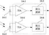
在图14中示出了光接收机的接收部分构成。两个通道的光电转换器(14-1、14-2)可以采用常用的PIN光电二极管或者硅光电二极管。它们的响应速度都很高,远远超出LED的响应速度,能够满足带宽要求。但是,它们的光谱响应特性有很多种类型,应尽量选择光谱的响应峰值和LED发光光谱峰值相匹配的类型。这类光电二极管的光谱响应峰值一般在550nm,光谱响应范围在350nm-800nm之间,可以根据所处通道选择不同的光电二极管。光电转换器后接互阻放大器(TIA,14-3、14-4),将光电流信号转换为电压信号,电压信号再经放大(14-5,14-6)后,送到后续的处理电路。两级放大器的带宽要足够适应光信号的带宽,这里可以取≥200MHz。FIG. 14 shows the configuration of the receiving section of the optical receiver. The photoelectric converters ( 14 - 1 , 14 - 2 ) of the two channels can adopt common PIN photodiodes or silicon photodiodes. Their response speed is very high, far beyond the response speed of LED, to meet the bandwidth requirements. However, there are many types of their spectral response characteristics, and you should try to choose the type whose spectral response peak matches the LED luminous spectrum peak. The peak spectral response of this type of photodiode is generally at 550nm, and the spectral response range is between 350nm and 800nm. Different photodiodes can be selected according to the channel they are in. The photoelectric converter is followed by a transimpedance amplifier (TIA, 14-3, 14-4), which converts the photocurrent signal into a voltage signal, and the voltage signal is then amplified (14-5, 14-6) and sent to subsequent processing circuit. The bandwidth of the two-stage amplifier should be sufficient to adapt to the bandwidth of the optical signal, which can be ≥200MHz here.
蓝光通道由于接收的是脉冲信号,受干扰的影响较小,也相对容易恢复同步信息。图9是正常接收的数据信号,由于OFDM调制了幅度、光信道衰落,以及背景光的干扰关系,存在一些脉冲幅度低于检测门限(Vt)的取样点,这种情形可以通过增强信道编码纠错能力降低误码率。为了确定OOK信号的帧边界以及辅助OFDM符号同步,在蓝光发射通道由(12-8)周期地插入一个同步头,结构如图10所示。这里由全幅度和半幅度的连续2个脉冲组合成1位信息。可以定义“高-低”脉冲组合代表“1”,“低-高”脉冲组合代表“0”,由此再构造成一个巴克码。图10中所示的就是一个“1110010”的7位巴克码。根据时钟频率及信道的稳定性,在发送的数据序列中周期地插入这样的脉冲串。以全幅度和半幅度构造同步序列的目的是在这个信号中容易获取接收信号的中间电平,以此可以确定OFDM信号的直流偏置,同时也容易对信道进行估计,提供均衡信息以及补偿LED的非线性。Since the Blu-ray channel receives pulse signals, it is less affected by interference, and it is relatively easy to restore synchronization information. Figure 9 shows the normally received data signal. Due to OFDM modulated amplitude, optical channel fading, and background light interference, there are some sampling points where the pulse amplitude is lower than the detection threshold (Vt ). This situation can be solved by enhancing the channel coding Error correction capability reduces bit error rate. In order to determine the frame boundary of the OOK signal and assist OFDM symbol synchronization, a synchronization header is periodically inserted into the blue light transmission channel by (12-8), and the structure is shown in FIG. 10 . Here, 2 continuous pulses of full amplitude and half amplitude are combined into 1 bit of information. It can be defined that the "high-low" pulse combination represents "1", and the "low-high" pulse combination represents "0", thus reconstructing a Barker code. What is shown in Fig. 10 is a 7-bit Barker code of "1110010". According to the clock frequency and the stability of the channel, such bursts are periodically inserted in the transmitted data sequence. The purpose of constructing the synchronization sequence with full amplitude and half amplitude is to easily obtain the intermediate level of the received signal in this signal, so as to determine the DC offset of the OFDM signal, and at the same time it is easy to estimate the channel, provide equalization information and compensate LED of non-linearity.
至此,实现一个“OOK-OFDM”调制的光收发机的基本实现步骤和主要设计参数已经叙述完毕。So far, the basic implementation steps and main design parameters of an "OOK-OFDM" modulated optical transceiver have been described.
上面所述虽然是针对白光LED的通信系统,但是这种双重调制的方法,包括双通道的OFDM信号合并、三个通道的辅助同步、OFDM调制补偿方法等,并不会仅仅局限于这种应用。比如,在超宽带通信系统或者光纤通信系统中,经过适当参数调整,也可以应用。Although the above is for the communication system of white light LEDs, this double modulation method, including two-channel OFDM signal combination, three-channel auxiliary synchronization, OFDM modulation compensation method, etc., is not limited to this application . For example, in an ultra-wideband communication system or an optical fiber communication system, it can also be applied after proper parameter adjustment.
Claims (7)
Priority Applications (1)
| Application Number | Priority Date | Filing Date | Title |
|---|---|---|---|
| CN 200910201114CN101710890B (en) | 2009-12-15 | 2009-12-15 | Pulse and OFDMD double-data modulation method |
Applications Claiming Priority (1)
| Application Number | Priority Date | Filing Date | Title |
|---|---|---|---|
| CN 200910201114CN101710890B (en) | 2009-12-15 | 2009-12-15 | Pulse and OFDMD double-data modulation method |
Publications (2)
| Publication Number | Publication Date |
|---|---|
| CN101710890Atrue CN101710890A (en) | 2010-05-19 |
| CN101710890B CN101710890B (en) | 2013-01-02 |
Family
ID=42403650
Family Applications (1)
| Application Number | Title | Priority Date | Filing Date |
|---|---|---|---|
| CN 200910201114Expired - Fee RelatedCN101710890B (en) | 2009-12-15 | 2009-12-15 | Pulse and OFDMD double-data modulation method |
Country Status (1)
| Country | Link |
|---|---|
| CN (1) | CN101710890B (en) |
Cited By (31)
| Publication number | Priority date | Publication date | Assignee | Title |
|---|---|---|---|---|
| CN102013174A (en)* | 2010-11-18 | 2011-04-13 | 华东理工大学 | Vehicle collision warning system based on optical communication |
| CN103166652A (en)* | 2011-12-15 | 2013-06-19 | 德克萨斯仪器股份有限公司 | Digital time-interleaved RF-PWM transmitter |
| CN103414514A (en)* | 2013-08-07 | 2013-11-27 | 武汉邮电科学研究院 | System and method for visible light communication based on OFDM modulation codes and frequency division receiving |
| CN103460629A (en)* | 2010-12-10 | 2013-12-18 | 阿尔卡特朗讯 | Coherent optical receiver for pilot-assisted data transmission |
| CN103716094A (en)* | 2014-01-06 | 2014-04-09 | 中国人民解放军信息工程大学 | Visible light communication front end circuit |
| CN103873143A (en)* | 2012-12-11 | 2014-06-18 | 松下电器产业株式会社 | Visible light communication device |
| CN104885381A (en)* | 2012-12-27 | 2015-09-02 | 松下电器(美国)知识产权公司 | Information communication method |
| CN105024754A (en)* | 2015-07-17 | 2015-11-04 | 清华大学 | Visible light communication method and device combining OOK modulation and OFDM modulation |
| CN105119655A (en)* | 2015-08-31 | 2015-12-02 | 华南理工大学 | Visible light communication method based on QAM and MPPM and system thereof |
| CN105743828A (en)* | 2015-09-23 | 2016-07-06 | 北京邮电大学 | Time slot interleaving-based optical amplitude phase modulation method |
| CN105915283A (en)* | 2016-04-08 | 2016-08-31 | 清华大学 | Bipolar signal-based visible light communication method and device |
| CN106130638A (en)* | 2016-08-20 | 2016-11-16 | 华南理工大学 | PAM Yu MPPM dual modulation method and system for visible light communication |
| CN106561004A (en)* | 2016-06-16 | 2017-04-12 | 中兴新能源汽车有限责任公司 | Wireless communication method and device |
| US9635278B2 (en) | 2012-12-27 | 2017-04-25 | Panasonic Intellectual Property Corporation Of America | Information communication method for obtaining information specified by striped pattern of bright lines |
| US9641766B2 (en) | 2012-12-27 | 2017-05-02 | Panasonic Intellectual Property Corporation Of America | Information communication method |
| US9646568B2 (en) | 2012-12-27 | 2017-05-09 | Panasonic Intellectual Property Corporation Of America | Display method |
| CN106717123A (en)* | 2014-06-27 | 2017-05-24 | 艾德拉博支持有限公司 | A method for driving a light source, a driver system to drive a light source and a luminaire comprising said light source and driver system |
| CN106797358A (en)* | 2014-07-23 | 2017-05-31 | 美国莱迪思半导体公司 | For the phase-modulation on-off keying of millimeter-wave spectrum control |
| US9768869B2 (en) | 2012-12-27 | 2017-09-19 | Panasonic Intellectual Property Corporation Of America | Information communication method |
| US9859980B2 (en) | 2012-12-27 | 2018-01-02 | Panasonic Intellectual Property Corporation Of America | Information processing program, reception program, and information processing apparatus |
| US9918016B2 (en) | 2012-12-27 | 2018-03-13 | Panasonic Intellectual Property Corporation Of America | Information communication apparatus, method, and recording medium using switchable normal mode and visible light communication mode |
| CN108092712A (en)* | 2017-12-08 | 2018-05-29 | 武汉邮电科学研究院 | Visible light communication system, method and application apparatus based on probability shaping coding |
| US9998220B2 (en) | 2012-12-27 | 2018-06-12 | Panasonic Intellectual Property Corporation Of America | Transmitting method, transmitting apparatus, and program |
| WO2018148864A1 (en)* | 2017-02-14 | 2018-08-23 | 华为技术有限公司 | Clock synchronization method and device |
| US10148354B2 (en) | 2012-12-27 | 2018-12-04 | Panasonic Intellectual Property Corporation Of America | Luminance change information communication method |
| US10225014B2 (en) | 2012-12-27 | 2019-03-05 | Panasonic Intellectual Property Corporation Of America | Information communication method for obtaining information using ID list and bright line image |
| US10303945B2 (en) | 2012-12-27 | 2019-05-28 | Panasonic Intellectual Property Corporation Of America | Display method and display apparatus |
| US10523876B2 (en) | 2012-12-27 | 2019-12-31 | Panasonic Intellectual Property Corporation Of America | Information communication method |
| US10530486B2 (en) | 2012-12-27 | 2020-01-07 | Panasonic Intellectual Property Corporation Of America | Transmitting method, transmitting apparatus, and program |
| CN111226423A (en)* | 2017-10-19 | 2020-06-02 | 瑞典爱立信有限公司 | Transmitter, network node, method and computer program for transmitting binary information |
| US10951310B2 (en) | 2012-12-27 | 2021-03-16 | Panasonic Intellectual Property Corporation Of America | Communication method, communication device, and transmitter |
Family Cites Families (1)
| Publication number | Priority date | Publication date | Assignee | Title |
|---|---|---|---|---|
| JP3827082B2 (en)* | 2002-10-24 | 2006-09-27 | 株式会社中川研究所 | Broadcast system, light bulb, lighting device |
- 2009
- 2009-12-15CNCN 200910201114patent/CN101710890B/ennot_activeExpired - Fee Related
Cited By (68)
| Publication number | Priority date | Publication date | Assignee | Title |
|---|---|---|---|---|
| CN102013174B (en)* | 2010-11-18 | 2015-12-02 | 华东理工大学 | Based on the vehicle collision prewarning system of optical communication |
| CN102013174A (en)* | 2010-11-18 | 2011-04-13 | 华东理工大学 | Vehicle collision warning system based on optical communication |
| CN103460629A (en)* | 2010-12-10 | 2013-12-18 | 阿尔卡特朗讯 | Coherent optical receiver for pilot-assisted data transmission |
| CN103460629B (en)* | 2010-12-10 | 2016-06-15 | 阿尔卡特朗讯 | Coherent optical receiver for pilot-aided data transmission |
| CN103166652A (en)* | 2011-12-15 | 2013-06-19 | 德克萨斯仪器股份有限公司 | Digital time-interleaved RF-PWM transmitter |
| CN103166652B (en)* | 2011-12-15 | 2017-03-01 | 德克萨斯仪器股份有限公司 | Interweave digit time RF PWM transmitter |
| CN103873143A (en)* | 2012-12-11 | 2014-06-18 | 松下电器产业株式会社 | Visible light communication device |
| CN103873143B (en)* | 2012-12-11 | 2017-04-12 | 松下知识产权经营株式会社 | Visible light communication device |
| US10218914B2 (en) | 2012-12-20 | 2019-02-26 | Panasonic Intellectual Property Corporation Of America | Information communication apparatus, method and recording medium using switchable normal mode and visible light communication mode |
| US10521668B2 (en) | 2012-12-27 | 2019-12-31 | Panasonic Intellectual Property Corporation Of America | Display method and display apparatus |
| US10530486B2 (en) | 2012-12-27 | 2020-01-07 | Panasonic Intellectual Property Corporation Of America | Transmitting method, transmitting apparatus, and program |
| US12088923B2 (en) | 2012-12-27 | 2024-09-10 | Panasonic Intellectual Property Corporation Of America | Information communication method |
| US11659284B2 (en) | 2012-12-27 | 2023-05-23 | Panasonic Intellectual Property Corporation Of America | Information communication method |
| US11490025B2 (en) | 2012-12-27 | 2022-11-01 | Panasonic Intellectual Property Corporation Of America | Information communication method |
| US11165967B2 (en) | 2012-12-27 | 2021-11-02 | Panasonic Intellectual Property Corporation Of America | Information communication method |
| US10951310B2 (en) | 2012-12-27 | 2021-03-16 | Panasonic Intellectual Property Corporation Of America | Communication method, communication device, and transmitter |
| US10887528B2 (en) | 2012-12-27 | 2021-01-05 | Panasonic Intellectual Property Corporation Of America | Information communication method |
| US10742891B2 (en) | 2012-12-27 | 2020-08-11 | Panasonic Intellectual Property Corporation Of America | Information communication method |
| US10666871B2 (en) | 2012-12-27 | 2020-05-26 | Panasonic Intellectual Property Corporation Of America | Information communication method |
| CN104885381A (en)* | 2012-12-27 | 2015-09-02 | 松下电器(美国)知识产权公司 | Information communication method |
| US9635278B2 (en) | 2012-12-27 | 2017-04-25 | Panasonic Intellectual Property Corporation Of America | Information communication method for obtaining information specified by striped pattern of bright lines |
| US9641766B2 (en) | 2012-12-27 | 2017-05-02 | Panasonic Intellectual Property Corporation Of America | Information communication method |
| US9646568B2 (en) | 2012-12-27 | 2017-05-09 | Panasonic Intellectual Property Corporation Of America | Display method |
| US10638051B2 (en) | 2012-12-27 | 2020-04-28 | Panasonic Intellectual Property Corporation Of America | Information communication method |
| US10616496B2 (en) | 2012-12-27 | 2020-04-07 | Panasonic Intellectual Property Corporation Of America | Information communication method |
| US10531009B2 (en) | 2012-12-27 | 2020-01-07 | Panasonic Intellectual Property Corporation Of America | Information communication method |
| US9756255B2 (en) | 2012-12-27 | 2017-09-05 | Panasonic Intellectual Property Corporation Of America | Information communication method |
| US9768869B2 (en) | 2012-12-27 | 2017-09-19 | Panasonic Intellectual Property Corporation Of America | Information communication method |
| US9794489B2 (en) | 2012-12-27 | 2017-10-17 | Panasonic Intellectual Property Corporation Of America | Information communication method |
| CN104885381B (en)* | 2012-12-27 | 2017-12-19 | 松下电器(美国)知识产权公司 | information communication method |
| US9859980B2 (en) | 2012-12-27 | 2018-01-02 | Panasonic Intellectual Property Corporation Of America | Information processing program, reception program, and information processing apparatus |
| US9918016B2 (en) | 2012-12-27 | 2018-03-13 | Panasonic Intellectual Property Corporation Of America | Information communication apparatus, method, and recording medium using switchable normal mode and visible light communication mode |
| US10531010B2 (en) | 2012-12-27 | 2020-01-07 | Panasonic Intellectual Property Corporation Of America | Information communication method |
| US9998220B2 (en) | 2012-12-27 | 2018-06-12 | Panasonic Intellectual Property Corporation Of America | Transmitting method, transmitting apparatus, and program |
| US10051194B2 (en) | 2012-12-27 | 2018-08-14 | Panasonic Intellectual Property Corporation Of America | Information communication method |
| US10523876B2 (en) | 2012-12-27 | 2019-12-31 | Panasonic Intellectual Property Corporation Of America | Information communication method |
| US10148354B2 (en) | 2012-12-27 | 2018-12-04 | Panasonic Intellectual Property Corporation Of America | Luminance change information communication method |
| US10165192B2 (en) | 2012-12-27 | 2018-12-25 | Panasonic Intellectual Property Corporation Of America | Information communication method |
| US10205887B2 (en) | 2012-12-27 | 2019-02-12 | Panasonic Intellectual Property Corporation Of America | Information communication method |
| US10516832B2 (en) | 2012-12-27 | 2019-12-24 | Panasonic Intellectual Property Corporation Of America | Information communication method |
| US10225014B2 (en) | 2012-12-27 | 2019-03-05 | Panasonic Intellectual Property Corporation Of America | Information communication method for obtaining information using ID list and bright line image |
| US10303945B2 (en) | 2012-12-27 | 2019-05-28 | Panasonic Intellectual Property Corporation Of America | Display method and display apparatus |
| US10334177B2 (en) | 2012-12-27 | 2019-06-25 | Panasonic Intellectual Property Corporation Of America | Information communication apparatus, method, and recording medium using switchable normal mode and visible light communication mode |
| US10354599B2 (en) | 2012-12-27 | 2019-07-16 | Panasonic Intellectual Property Corporation Of America | Display method |
| US10361780B2 (en) | 2012-12-27 | 2019-07-23 | Panasonic Intellectual Property Corporation Of America | Information processing program, reception program, and information processing apparatus |
| US10368006B2 (en) | 2012-12-27 | 2019-07-30 | Panasonic Intellectual Property Corporation Of America | Information communication method |
| US10368005B2 (en) | 2012-12-27 | 2019-07-30 | Panasonic Intellectual Property Corporation Of America | Information communication method |
| US10455161B2 (en) | 2012-12-27 | 2019-10-22 | Panasonic Intellectual Property Corporation Of America | Information communication method |
| US10447390B2 (en) | 2012-12-27 | 2019-10-15 | Panasonic Intellectual Property Corporation Of America | Luminance change information communication method |
| CN103414514A (en)* | 2013-08-07 | 2013-11-27 | 武汉邮电科学研究院 | System and method for visible light communication based on OFDM modulation codes and frequency division receiving |
| CN103414514B (en)* | 2013-08-07 | 2015-09-16 | 武汉邮电科学研究院 | The visible light communication system received based on OFDM modulation coding and frequency division and method |
| CN103716094A (en)* | 2014-01-06 | 2014-04-09 | 中国人民解放军信息工程大学 | Visible light communication front end circuit |
| CN103716094B (en)* | 2014-01-06 | 2016-06-01 | 中国人民解放军信息工程大学 | A kind of visible light communication front end circuit |
| CN106717123A (en)* | 2014-06-27 | 2017-05-24 | 艾德拉博支持有限公司 | A method for driving a light source, a driver system to drive a light source and a luminaire comprising said light source and driver system |
| CN106797358A (en)* | 2014-07-23 | 2017-05-31 | 美国莱迪思半导体公司 | For the phase-modulation on-off keying of millimeter-wave spectrum control |
| CN106797358B (en)* | 2014-07-23 | 2020-01-07 | 美国莱迪思半导体公司 | Phase modulation on-off keying for millimeter wave spectrum control |
| WO2017012452A1 (en)* | 2015-07-17 | 2017-01-26 | 清华大学 | Visible light communication method and device fusing ook modulation and ofdm modulation |
| CN105024754B (en)* | 2015-07-17 | 2017-07-28 | 清华大学 | Merge the visible light communication method and device that OOK modulation and OFDM are modulated |
| CN105024754A (en)* | 2015-07-17 | 2015-11-04 | 清华大学 | Visible light communication method and device combining OOK modulation and OFDM modulation |
| CN105119655A (en)* | 2015-08-31 | 2015-12-02 | 华南理工大学 | Visible light communication method based on QAM and MPPM and system thereof |
| CN105743828A (en)* | 2015-09-23 | 2016-07-06 | 北京邮电大学 | Time slot interleaving-based optical amplitude phase modulation method |
| CN105915283A (en)* | 2016-04-08 | 2016-08-31 | 清华大学 | Bipolar signal-based visible light communication method and device |
| CN106561004A (en)* | 2016-06-16 | 2017-04-12 | 中兴新能源汽车有限责任公司 | Wireless communication method and device |
| CN106130638A (en)* | 2016-08-20 | 2016-11-16 | 华南理工大学 | PAM Yu MPPM dual modulation method and system for visible light communication |
| WO2018148864A1 (en)* | 2017-02-14 | 2018-08-23 | 华为技术有限公司 | Clock synchronization method and device |
| CN111226423A (en)* | 2017-10-19 | 2020-06-02 | 瑞典爱立信有限公司 | Transmitter, network node, method and computer program for transmitting binary information |
| CN108092712A (en)* | 2017-12-08 | 2018-05-29 | 武汉邮电科学研究院 | Visible light communication system, method and application apparatus based on probability shaping coding |
| CN108092712B (en)* | 2017-12-08 | 2019-08-27 | 武汉邮电科学研究院 | Visible light communication system, method and application apparatus based on probability shaping coding |
Also Published As
| Publication number | Publication date |
|---|---|
| CN101710890B (en) | 2013-01-02 |
Similar Documents
| Publication | Publication Date | Title |
|---|---|---|
| CN101710890A (en) | Pulse and OFDMD double-data modulation method | |
| Wang et al. | High speed WDM VLC system based on multi-band CAP64 with weighted pre-equalization and modified CMMA based post-equalization | |
| Islim et al. | Modulation techniques for li-fi | |
| Karunatilaka et al. | LED based indoor visible light communications: State of the art | |
| Khalid et al. | 1-Gb/s transmission over a phosphorescent white LED by using rate-adaptive discrete multitone modulation | |
| Khalighi et al. | PAM-and CAP-based transmission schemes for visible-light communications | |
| CN103595688B (en) | Visible light communication multiple access method based on no-load Amplitude Phase Modulation and system | |
| Cossu et al. | 2.1 Gbit/s visible optical wireless transmission | |
| CN103731208B (en) | Transmission equipment and reception Apparatus for () and method therefor for visible light communication | |
| Medina et al. | Led based visible light communication: Technology, applications and challenges-a survey | |
| Noshad et al. | Can visible light communications provide Gb/s service? | |
| Wang et al. | 875-Mb/s asynchronous bi-directional 64QAM-OFDM SCM-WDM transmission over RGB-LED-based visible light communication system | |
| CN105119655A (en) | Visible light communication method based on QAM and MPPM and system thereof | |
| Dahri et al. | A review of modulation schemes for visible light communication | |
| CN103414514B (en) | The visible light communication system received based on OFDM modulation coding and frequency division and method | |
| Li et al. | 682 Mbit/s phosphorescent white LED visible light communications utilizing analog equalized 16QAM-OFDM modulation without blue filter | |
| Wang et al. | 3.25-Gbps visible light communication system based on single carrier frequency domain equalization utilizing an RGB LED | |
| CN106160873A (en) | A kind of phase-shift coding method based on pulse amplitude modulation system and realize device | |
| Cossu et al. | Long distance indoor high speed visible light communication system based on RGB LEDs | |
| Qian et al. | A robust CDMA VLC system against front-end nonlinearity | |
| CN104022822A (en) | RGB-type LED-based visible light communication frequency modulation method | |
| CN104038283A (en) | LED lighting communication system | |
| CN113193913B (en) | Visible light communication system and method based on MPPM and self-adaptive bias | |
| CN204068977U (en) | LED lighting communication system | |
| Mirvakili et al. | Wireless access test-bed through visible light and dimming compatible OFDM |
Legal Events
| Date | Code | Title | Description |
|---|---|---|---|
| C06 | Publication | ||
| PB01 | Publication | ||
| C10 | Entry into substantive examination | ||
| SE01 | Entry into force of request for substantive examination | ||
| C14 | Grant of patent or utility model | ||
| GR01 | Patent grant | ||
| DD01 | Delivery of document by public notice | Addressee:East China University of Science and Technology Document name:Notification to Pay the Fees | |
| CF01 | Termination of patent right due to non-payment of annual fee | ||
| CF01 | Termination of patent right due to non-payment of annual fee | Granted publication date:20130102 Termination date:20161215 |