CN101685780A - Semiconductor device and method of manufacturing a semiconductor device with a metal gate stack - Google Patents
Semiconductor device and method of manufacturing a semiconductor device with a metal gate stackDownload PDFInfo
- Publication number
- CN101685780A CN101685780ACN200910166436ACN200910166436ACN101685780ACN 101685780 ACN101685780 ACN 101685780ACN 200910166436 ACN200910166436 ACN 200910166436ACN 200910166436 ACN200910166436 ACN 200910166436ACN 101685780 ACN101685780 ACN 101685780A
- Authority
- CN
- China
- Prior art keywords
- layer
- metal
- semiconductor device
- semiconductor
- gate
- Prior art date
- Legal status (The legal status is an assumption and is not a legal conclusion. Google has not performed a legal analysis and makes no representation as to the accuracy of the status listed.)
- Pending
Links
Images


Classifications
- H—ELECTRICITY
- H01—ELECTRIC ELEMENTS
- H01L—SEMICONDUCTOR DEVICES NOT COVERED BY CLASS H10
- H01L21/00—Processes or apparatus adapted for the manufacture or treatment of semiconductor or solid state devices or of parts thereof
- H01L21/02—Manufacture or treatment of semiconductor devices or of parts thereof
- H01L21/04—Manufacture or treatment of semiconductor devices or of parts thereof the devices having potential barriers, e.g. a PN junction, depletion layer or carrier concentration layer
- H01L21/18—Manufacture or treatment of semiconductor devices or of parts thereof the devices having potential barriers, e.g. a PN junction, depletion layer or carrier concentration layer the devices having semiconductor bodies comprising elements of Group IV of the Periodic Table or AIIIBV compounds with or without impurities, e.g. doping materials
- H01L21/28—Manufacture of electrodes on semiconductor bodies using processes or apparatus not provided for in groups H01L21/20 - H01L21/268
- H01L21/28008—Making conductor-insulator-semiconductor electrodes
- H01L21/28017—Making conductor-insulator-semiconductor electrodes the insulator being formed after the semiconductor body, the semiconductor being silicon
- H01L21/28026—Making conductor-insulator-semiconductor electrodes the insulator being formed after the semiconductor body, the semiconductor being silicon characterised by the conductor
- H01L21/28088—Making conductor-insulator-semiconductor electrodes the insulator being formed after the semiconductor body, the semiconductor being silicon characterised by the conductor the final conductor layer next to the insulator being a composite, e.g. TiN
- H—ELECTRICITY
- H10—SEMICONDUCTOR DEVICES; ELECTRIC SOLID-STATE DEVICES NOT OTHERWISE PROVIDED FOR
- H10D—INORGANIC ELECTRIC SEMICONDUCTOR DEVICES
- H10D30/00—Field-effect transistors [FET]
- H10D30/60—Insulated-gate field-effect transistors [IGFET]
- H—ELECTRICITY
- H10—SEMICONDUCTOR DEVICES; ELECTRIC SOLID-STATE DEVICES NOT OTHERWISE PROVIDED FOR
- H10D—INORGANIC ELECTRIC SEMICONDUCTOR DEVICES
- H10D30/00—Field-effect transistors [FET]
- H10D30/60—Insulated-gate field-effect transistors [IGFET]
- H10D30/601—Insulated-gate field-effect transistors [IGFET] having lightly-doped drain or source extensions, e.g. LDD IGFETs or DDD IGFETs
- H—ELECTRICITY
- H10—SEMICONDUCTOR DEVICES; ELECTRIC SOLID-STATE DEVICES NOT OTHERWISE PROVIDED FOR
- H10D—INORGANIC ELECTRIC SEMICONDUCTOR DEVICES
- H10D30/00—Field-effect transistors [FET]
- H10D30/60—Insulated-gate field-effect transistors [IGFET]
- H10D30/791—Arrangements for exerting mechanical stress on the crystal lattice of the channel regions
- H10D30/794—Arrangements for exerting mechanical stress on the crystal lattice of the channel regions comprising conductive materials, e.g. silicided source, drain or gate electrodes
- H—ELECTRICITY
- H10—SEMICONDUCTOR DEVICES; ELECTRIC SOLID-STATE DEVICES NOT OTHERWISE PROVIDED FOR
- H10D—INORGANIC ELECTRIC SEMICONDUCTOR DEVICES
- H10D64/00—Electrodes of devices having potential barriers
- H10D64/60—Electrodes characterised by their materials
- H10D64/66—Electrodes having a conductor capacitively coupled to a semiconductor by an insulator, e.g. MIS electrodes
- H10D64/667—Electrodes having a conductor capacitively coupled to a semiconductor by an insulator, e.g. MIS electrodes the conductor comprising a layer of alloy material, compound material or organic material contacting the insulator, e.g. TiN workfunction layers
- H—ELECTRICITY
- H10—SEMICONDUCTOR DEVICES; ELECTRIC SOLID-STATE DEVICES NOT OTHERWISE PROVIDED FOR
- H10D—INORGANIC ELECTRIC SEMICONDUCTOR DEVICES
- H10D30/00—Field-effect transistors [FET]
- H10D30/01—Manufacture or treatment
- H10D30/021—Manufacture or treatment of FETs having insulated gates [IGFET]
- H10D30/0223—Manufacture or treatment of FETs having insulated gates [IGFET] having source and drain regions or source and drain extensions self-aligned to sides of the gate
- H10D30/0227—Manufacture or treatment of FETs having insulated gates [IGFET] having source and drain regions or source and drain extensions self-aligned to sides of the gate having both lightly-doped source and drain extensions and source and drain regions self-aligned to the sides of the gate, e.g. lightly-doped drain [LDD] MOSFET or double-diffused drain [DDD] MOSFET
- H—ELECTRICITY
- H10—SEMICONDUCTOR DEVICES; ELECTRIC SOLID-STATE DEVICES NOT OTHERWISE PROVIDED FOR
- H10D—INORGANIC ELECTRIC SEMICONDUCTOR DEVICES
- H10D64/00—Electrodes of devices having potential barriers
- H10D64/01—Manufacture or treatment
- H10D64/017—Manufacture or treatment using dummy gates in processes wherein at least parts of the final gates are self-aligned to the dummy gates, i.e. replacement gate processes
- H—ELECTRICITY
- H10—SEMICONDUCTOR DEVICES; ELECTRIC SOLID-STATE DEVICES NOT OTHERWISE PROVIDED FOR
- H10D—INORGANIC ELECTRIC SEMICONDUCTOR DEVICES
- H10D64/00—Electrodes of devices having potential barriers
- H10D64/60—Electrodes characterised by their materials
- H10D64/66—Electrodes having a conductor capacitively coupled to a semiconductor by an insulator, e.g. MIS electrodes
- H10D64/68—Electrodes having a conductor capacitively coupled to a semiconductor by an insulator, e.g. MIS electrodes characterised by the insulator, e.g. by the gate insulator
- H10D64/691—Electrodes having a conductor capacitively coupled to a semiconductor by an insulator, e.g. MIS electrodes characterised by the insulator, e.g. by the gate insulator comprising metallic compounds, e.g. metal oxides or metal silicates
- H—ELECTRICITY
- H10—SEMICONDUCTOR DEVICES; ELECTRIC SOLID-STATE DEVICES NOT OTHERWISE PROVIDED FOR
- H10D—INORGANIC ELECTRIC SEMICONDUCTOR DEVICES
- H10D84/00—Integrated devices formed in or on semiconductor substrates that comprise only semiconducting layers, e.g. on Si wafers or on GaAs-on-Si wafers
- H10D84/01—Manufacture or treatment
- H10D84/0123—Integrating together multiple components covered by H10D12/00 or H10D30/00, e.g. integrating multiple IGBTs
- H10D84/0126—Integrating together multiple components covered by H10D12/00 or H10D30/00, e.g. integrating multiple IGBTs the components including insulated gates, e.g. IGFETs
- H10D84/0165—Integrating together multiple components covered by H10D12/00 or H10D30/00, e.g. integrating multiple IGBTs the components including insulated gates, e.g. IGFETs the components including complementary IGFETs, e.g. CMOS devices
- H10D84/0167—Manufacturing their channels
- H—ELECTRICITY
- H10—SEMICONDUCTOR DEVICES; ELECTRIC SOLID-STATE DEVICES NOT OTHERWISE PROVIDED FOR
- H10D—INORGANIC ELECTRIC SEMICONDUCTOR DEVICES
- H10D84/00—Integrated devices formed in or on semiconductor substrates that comprise only semiconducting layers, e.g. on Si wafers or on GaAs-on-Si wafers
- H10D84/01—Manufacture or treatment
- H10D84/0123—Integrating together multiple components covered by H10D12/00 or H10D30/00, e.g. integrating multiple IGBTs
- H10D84/0126—Integrating together multiple components covered by H10D12/00 or H10D30/00, e.g. integrating multiple IGBTs the components including insulated gates, e.g. IGFETs
- H10D84/0165—Integrating together multiple components covered by H10D12/00 or H10D30/00, e.g. integrating multiple IGBTs the components including insulated gates, e.g. IGFETs the components including complementary IGFETs, e.g. CMOS devices
- H10D84/0172—Manufacturing their gate conductors
- H10D84/0174—Manufacturing their gate conductors the gate conductors being silicided
- H—ELECTRICITY
- H10—SEMICONDUCTOR DEVICES; ELECTRIC SOLID-STATE DEVICES NOT OTHERWISE PROVIDED FOR
- H10D—INORGANIC ELECTRIC SEMICONDUCTOR DEVICES
- H10D84/00—Integrated devices formed in or on semiconductor substrates that comprise only semiconducting layers, e.g. on Si wafers or on GaAs-on-Si wafers
- H10D84/01—Manufacture or treatment
- H10D84/02—Manufacture or treatment characterised by using material-based technologies
- H10D84/03—Manufacture or treatment characterised by using material-based technologies using Group IV technology, e.g. silicon technology or silicon-carbide [SiC] technology
- H10D84/038—Manufacture or treatment characterised by using material-based technologies using Group IV technology, e.g. silicon technology or silicon-carbide [SiC] technology using silicon technology, e.g. SiGe
Landscapes
- Engineering & Computer Science (AREA)
- Chemical & Material Sciences (AREA)
- Composite Materials (AREA)
- Physics & Mathematics (AREA)
- Condensed Matter Physics & Semiconductors (AREA)
- General Physics & Mathematics (AREA)
- Manufacturing & Machinery (AREA)
- Computer Hardware Design (AREA)
- Microelectronics & Electronic Packaging (AREA)
- Power Engineering (AREA)
- Insulated Gate Type Field-Effect Transistor (AREA)
- Electrodes Of Semiconductors (AREA)
Abstract
Description
Translated fromChinese技术领域technical field
本发明涉及制造具有金属栅极堆叠的半导体装置的方法。The present invention relates to methods of fabricating semiconductor devices having metal gate stacks.
背景技术Background technique
当例如金属氧化物半导体场效应晶体管(metal-oxide-semiconductorfield-effect transistor;MOSFET)的半导体装置随着各种技术节点(technologynode)微缩化时,高介电常数(high k)介电材料与金属被用来形成栅极堆叠。此外,使用应变硅(strained silicon)以提高晶体管通道的迁移率(mobility)。于一般的方法中,是使用氮化硅层、离子注入以及退火工艺以形成应变基底。另一方面,调整功函数以增进装置效能。当考虑高介电常数介电材料层非常薄时,电流通道会损坏高介电常数介电材料层与基底。再者,上述形成应变基底的方法难以达到大应力。When semiconductor devices such as metal-oxide-semiconductor field-effect transistors (MOSFETs) are miniaturized along with various technology nodes (technology nodes), high dielectric constant (high k) dielectric materials and metal are used to form gate stacks. In addition, strained silicon is used to increase the mobility of the transistor channel. In a typical method, a silicon nitride layer, ion implantation and annealing process are used to form a strained substrate. On the other hand, the work function is adjusted to enhance device performance. When considering that the high-k dielectric material layer is very thin, the current path will damage the high-k dielectric material layer and the substrate. Furthermore, it is difficult to achieve large stress in the above-mentioned method of forming a strained substrate.
发明内容Contents of the invention
本发明提供一种制造具有金属栅极堆叠的半导体装置的方法,包括:于一半导体基底上形成一高介电常数介电材料层;于该高介电常数介电材料层上形成一第一金属层;于该第一金属层上形成一硅层;图案化该硅层、第一金属层及高介电常数介电材料层以形成具有一栅极长度小于50nm的栅极堆叠;以及进行硅化工艺以将该硅层完全转变成一硅化电极。The invention provides a method for manufacturing a semiconductor device with a metal gate stack, comprising: forming a high-permittivity dielectric material layer on a semiconductor substrate; forming a first high-permittivity dielectric material layer on the high-permittivity dielectric material layer metal layer; forming a silicon layer on the first metal layer; patterning the silicon layer, the first metal layer, and the high-k dielectric material layer to form a gate stack having a gate length less than 50 nm; and performing A silicidation process to completely transform the silicon layer into a silicided electrode.
本发明也提供一种制造具有金属栅极堆叠的半导体装置的方法,包括:于一半导体基底上形成一栅极堆叠;于该半导体基底中形成一源极及漏极;于该源极及漏极上形成一第一硅化层;于该半导体基底上形成一层间介电材料层;对该半导体基底进行一化学机械研磨工艺;以及之后,于该栅极堆叠上形成一第二硅化层。The present invention also provides a method of manufacturing a semiconductor device with a metal gate stack, comprising: forming a gate stack on a semiconductor substrate; forming a source and a drain in the semiconductor substrate; forming a first silicide layer on the electrode; forming an interlayer dielectric material layer on the semiconductor substrate; performing a chemical mechanical polishing process on the semiconductor substrate; and then forming a second silicide layer on the gate stack.
本发明还提供一种半导体装置,包括:一源极及漏极,位于一半导体基底中;一第一栅极堆叠,设置于该半导体基底中且插介于该源极及该漏极之间,其中该第一栅极堆叠具有小于50nm的栅极长度且包括:一高介电常数介电层,设置于该半导体基底上;一第一金属层,设置于该高介电常数介电层上;以及一硅化栅极层,直接设置于该第一金属层上,该硅化栅极层具有一第一厚度;以及硅化元件,形成于该源极及该漏极上,该些硅化元件具有实质上小于该第一厚度的一第二厚度。The present invention also provides a semiconductor device, comprising: a source and a drain located in a semiconductor substrate; a first gate stack disposed in the semiconductor substrate and interposed between the source and the drain , wherein the first gate stack has a gate length of less than 50 nm and includes: a high-k dielectric layer disposed on the semiconductor substrate; a first metal layer disposed on the high-k dielectric layer and a silicided gate layer, disposed directly on the first metal layer, the silicided gate layer has a first thickness; and silicided elements, formed on the source and the drain, the silicided elements have A second thickness substantially smaller than the first thickness.
本发明提供具有金属栅极堆叠的半导体装置,其中当硅层转变成硅化层时,金属层混合硅层,且在栅极堆叠中造成应力。本发明中,应力与功函数可分开设计并适当的调整,本发明也消除了一般方法中由应力对高介电常数介电材料与基底所造成的损坏。The present invention provides a semiconductor device with a metal gate stack, wherein when the silicon layer is transformed into a silicide layer, the metal layer mixes with the silicon layer and causes stress in the gate stack. In the present invention, the stress and the work function can be designed separately and adjusted appropriately, and the present invention also eliminates the damage caused by the stress to the high dielectric constant dielectric material and the substrate in the general method.
附图说明Description of drawings
图1是根据本发明概念所构成的制造具有金属栅极结构的半导体装置的方法流程图。FIG. 1 is a flowchart of a method for fabricating a semiconductor device with a metal gate structure according to the concept of the present invention.
图2至图5是于各种实施例中根据本发明概念所构成的具有金属栅极结构的半导体装置的剖面图。2 to 5 are cross-sectional views of semiconductor devices with metal gate structures constructed according to the concepts of the present invention in various embodiments.
图6是根据本发明概念所构成的制造具有金属栅极结构的半导体装置的方法流程图。FIG. 6 is a flow chart of a method for fabricating a semiconductor device with a metal gate structure according to the concept of the present invention.
图7至图10是于各种实施例中根据本发明概念所构成的具有金属栅极结构的半导体装置的剖面图。7 to 10 are cross-sectional views of semiconductor devices with metal gate structures constructed according to the concepts of the present invention in various embodiments.
并且,上述附图中的附图标记说明如下:And, the reference numerals in the above-mentioned accompanying drawings are explained as follows:
210~半导体基底;212~高介电常数介电材料层;214~金属层;216~硅层;218~硬掩模层;220~介电层;222~间隙壁;224~源极/漏极;226~源极/漏极硅化物;228~硅化层;229~层间介电层。210~semiconductor substrate; 212~high dielectric constant dielectric material layer; 214~metal layer; 216~silicon layer; 218~hard mask layer; 220~dielectric layer; 222~spacer; 224~source/drain pole; 226~source/drain silicide; 228~silicide layer; 229~interlayer dielectric layer.
具体实施方式Detailed ways
有关各实施例的制造和使用方式如以下所详述。然而,值得注意的是,本发明所提供的各种可应用的发明概念是依具体内文的各种变化据以实施,且在此所讨论的具体实施例仅是用来显示具体使用和制造本发明的方法,而不用以限制本发明的范围。以下是通过各种附图及实施例说明本发明较佳实施例的制造过程。在本发明各种不同的各种实施例和附图中,相同的符号代表相同或类似的元件。此外,当一层材料层是位于另一材料层或基板之上时,其可以是直接位于其表面上或另外插入有其他中介层。The manner in which the various embodiments can be made and used are described in detail below. However, it should be noted that the various applicable inventive concepts provided by the present invention are implemented according to various changes in the specific context, and the specific embodiments discussed here are only used to show the specific use and manufacture The method of the present invention is not intended to limit the scope of the present invention. The following is a description of the manufacturing process of the preferred embodiment of the present invention through various drawings and examples. In the various and various embodiments of the invention and in the drawings, the same reference numerals represent the same or similar elements. Furthermore, when a material layer is on top of another material layer or substrate, it may be directly on its surface or additionally interposed with other intervening layers.
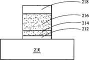
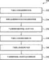
图1是根据本发明概念所构成的制造具有金属栅极结构的半导体装置的方法100。图2至图5是于各种实施例中根据本发明概念所构成的具有金属栅极结构的半导体装置200的剖面图。以下说明半导体装置200及其制造方法100。FIG. 1 illustrates a
请参考图1及图2,方法100起始于步骤102,于半导体基底210上形成各种栅极材料层。半导体基底210包括硅。基底还包括各种隔离元件,例如浅沟槽隔离(shallow trench isolation;STI),以及各种掺杂元件,例如通过公知的各种离子注入或扩散技术所形成的n型阱及p型阱。基底210可额外的包括锗(germanium)、硅锗(silicon germanium)或其他合适的半导体材料。于其他实施例中,基底210可额外的包括其他半导体材料,例如钻石(diamond)、碳化硅(silicon carbide)、砷化镓(gallium arsenic)、磷砷化镓(GaAsP)、砷化铝铟(AlInAs)、砷化铝镓(AlGaAs)、磷化镓铟(GaInP)、或其他适当的其组合。Please refer to FIG. 1 and FIG. 2 , the
于此步骤,高介电常数介电材料层212形成于基底上。通过例如原子层沉积法(atomic layer deposition;ALD)的适合步骤形成高介电常数介电材料层212。其他形成高介电常数介电材料层的方法包括金属有机化学气相沉积法(metal organic chemical vapor deposition;MOCVD)、物理气相沉积法(physicalvapor deposition;PVD)、紫外线-臭氧氧化(UV-Ozone Oxidation)法以及分子束外延法(molecular beam epitaxy;MBE)。于一实施例中,高介电常数介电材料包括氧化铪(HfO2)。或者,高介电常数介电材料层包括金属氮化物(metalnitride)、金属硅化物(metal silicates)或其他金属氧化物(metal oxide)。In this step, a high-k
可额外的于基底上形成界面层(interfacial layer;IL)(未显示),且界面层插介于半导体基底210及高介电常数介电材料层212之间。于一例子中,界面层包括薄氧化硅层。薄氧化硅是在形成高介电常数介电材料层前形成于基底210上。薄氧化硅层可以原子层沉积法或热氧化法形成。An interfacial layer (interfacial layer; IL) (not shown) may be additionally formed on the substrate, and the interfacial layer is interposed between the
金属层214形成于高介电常数介电材料层上。金属层214是以PVD或其他合适的方法形成。于一实施例中,金属层包括氮化钛(titanium nitride)。于其他实施例中,金属栅极层可包括氮化钽(tantalum nitride)、氮化钼(molybdenum nitride)、氮化钨(tungsten nitride)、钨(tungsten)、碳化钽(tantalumcarbide)、氮碳化钽(tantalum carbide nitride)、氮化钛铝(titanium aluminumnitride)或其组合。所选择的金属层具有适当的功函数。于一实施例中,金属层214的厚度小于约50埃(angstrom)。于其他实施例中,金属层可具有设计成具有适当功函数的多层膜结构(multi-film structure)。The
可设置盖层(capping layer)(未显示)于高介电常数介电材料层上。盖层插介于高介电常数介电材料层及金属层之间。于一实施例中,盖层包括氧化镧(lanthanum oxide;LaO)。盖层或者可包括其他合适的材料,例如氧化铝(aluminum oxide;Al2O3)。盖层可以合适的方法形成,例如PVD或ALD法。A capping layer (not shown) can be disposed on the high-k dielectric material layer. The capping layer is interposed between the high-k dielectric material layer and the metal layer. In one embodiment, the capping layer includes lanthanum oxide (LaO). The capping layer may alternatively comprise other suitable materials such as aluminum oxide (Al2 O3 ). The cap layer can be formed by a suitable method, such as PVD or ALD.
硅层216还形成于金属层214上。于一实施例中,硅层包括多晶硅。于其他实施例中,硅层包括非晶硅。可以化学气相沉积(CVD)工艺形成硅层。可于CVD工艺中使用硅烷(silane;SiH4)作为化学气体以形成硅层。于一实施例中,硅层的厚度小于约700埃。举例而言,硅层的厚度为约600埃。A
可还于硅层216上形成硬掩模层218以图案化栅极。硬掩模层218包括一或多种介电材料,且利用合适的方法形成,例如CVD法。于各种实施例中,硬掩模层包括氧化硅、氮化硅、氮氧化硅或于多层膜结构中的其组合物。A
请参考图1及图2,方法100进行至步骤104,图案化各种栅极材料层以形成栅极堆叠。于硬掩模层上形成定义一或多个开口的图案化光致抗蚀剂层。然后蚀刻移除于图案化光致抗蚀剂层的开口中的硬掩模层,以形成图案化硬掩模层。对硬掩模层所进行的蚀刻工艺可为湿蚀刻工艺或干蚀刻工艺。举例而言,可使用氢氟酸(hydrofluoric;HF)溶液蚀刻氧化硅硬掩模层。可利用光刻制成形成图案化光致抗蚀剂层。光刻工艺的例子可包括光致抗蚀剂层涂布、软烤(soft baking)、遮罩对准、曝光、曝光后烘烤(post-exposure baking)、显影(developing photoresist)及硬烤(hard baking)的工艺步骤。也可以例如无光罩光刻(maskless photolithography)、电子束刻写(electron-beam writing)、离子束刻写(ion-beam writing)及分子转印(molecular imprint)的其他适合的方法进行或取代光刻曝光工艺。或者,可不使用硬掩模层。于此例子中,是通过于硅层上直接形成图案化光致抗蚀剂层,然后利用图案化光致抗蚀剂层作为蚀刻掩模以蚀刻栅极层而图案化栅极层。Referring to FIG. 1 and FIG. 2 , the
然后通过蚀刻工艺(etching process)将于图案化硬掩模层的开口中的各种栅极材料层蚀刻移除。于一实施例中,蚀刻工艺使用干蚀刻工艺。于一实施例中,干蚀刻工艺使用含氟等离子体移除硅层。于其他实施例中,干蚀刻工艺使用含氟等离子体移除硅层、金属层及高介电常数介电材料层。于例子的进化中,蚀刻气体包括CF4。或者,蚀刻工艺可包括多个蚀刻步骤以蚀刻各种栅极材料层。于一实施例中,栅极堆叠具有小于50nm的栅极宽度。Then, various gate material layers in the openings of the patterned hard mask layer are etched away by an etching process. In one embodiment, the etching process uses a dry etching process. In one embodiment, the dry etch process uses a fluorine-containing plasma to remove the silicon layer. In other embodiments, the dry etching process uses a fluorine-containing plasma to remove the silicon layer, the metal layer, and the high-k dielectric material layer. In a variation of the example, the etching gas includesCF4 . Alternatively, the etch process may include multiple etch steps to etch various gate material layers. In one embodiment, the gate stack has a gate width less than 50 nm.
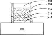
请参考图1及图3,方法100可进行至步骤106,于栅极堆叠的侧壁上形成介电层220。于栅极堆叠的侧壁上设置介电层220使后续形成的源极/漏极元件自栅极堆叠偏移而增进元件效能。此外或或者,使用介电层封住高介电常数介电材料层及金属以保护这些栅极材料。介电层220包括氧化硅、氮化硅或其他适合的介电材料。可以CVD、PVD或其他合适的方法形成介电层220。Referring to FIG. 1 and FIG. 3 , the
请参考图1及图4,方法100进行至步骤108,于基底210上形成各种源极及漏极元件。于一实施例中,通过利用栅极堆叠作为注入掩模进行离子注入步骤而形成轻掺杂漏极(lightly doped drain;LDD)区域。轻掺杂漏极区域大体对准于栅极堆叠的边缘。若介电层存在,轻掺杂漏极区域通过介电层自栅极堆叠的边缘偏移。此外,可进行口袋离子注入步骤以消除短通道效应。Referring to FIG. 1 and FIG. 4 , the
然后通过公知技术于栅极堆叠的侧壁(或介电层的侧壁,若存在时)上形成间隙壁222。举例而言,间隙壁包括氮化硅且是以化学气相沉积以及然后干蚀刻工艺形成。间隙壁222可具有多层结构。
然后通过另一离子注入工艺于基底中形成源极与漏极。因此所形成的源极与漏极是通过间隙壁222更偏移自栅极堆叠。轻掺杂漏极区域及源极/漏极于图4中皆标示为224。此后对基底进行退火工艺以活化源极/漏极元件224。可利用适合的方法进行退火工艺,例如快速热退火(rapid thermal annealing)或激光退火(laser annealing)法。Then another ion implantation process is used to form source and drain in the substrate. The source and drain are thus formed more offset from the gate stack by the
通过蚀刻工艺将硬掩模218自栅极堆叠移除。举例而言,若硬掩模由氮化硅所构成,使用热磷酸(phosphoric acid;H3PO4)溶液作为蚀刻剂以选择性的移除硬掩模层。于一实施例中,可在形成源极与漏极的离子注入步骤后移除硬掩模。于其他实施例中,在间隙壁222形成后,用以形成源极与漏极的第二离子注入步骤前,移除硬掩模层。The
请参考图1及图5,方法100进行至步骤110,于栅极堆叠上形成完全硅化层(fully silicide layer)228。硅层216使用自对准硅化技术(self-alignedsilicide technique)完全变成硅化层228。于一形成完全硅化层的程序的实施例中,是首先于基底上沉积第二金属层。第二金属层直接接触于栅极区中的硅层。接着以适当的温度对半导体装置200进行退火工艺以使第二金属层与硅层反应形成硅化物。进行退火工艺直到硅层完全转变成硅化层。在退火工艺后将未反应的金属自基底移除。Referring to FIG. 1 and FIG. 5 , the
于各种实施例中用以形成硅化物的金属材料包括钛(titanium)、镍(nickel)、钴(cobalt)、铂(platinum)、钯(palladium)、钨(tungsten)、钽(tantalum)或铒(erbium)。所形成的硅化物可为任何适当的组成(composition)及相(phase),其取决于各种参数,包括退火温度与第二金属层的厚度。于一实施例中,硅化层228具有梯度结构(graded structure),使得硅化物组成/相可垂直的改变。于其他实施例中,硅化层228具有例如MSi、MSi2、M2Si、M2Si3、M3Si2或M3Si的相/组成,例如其中的“M”表示第二金属。Metal materials used to form silicide in various embodiments include titanium (titanium), nickel (nickel), cobalt (cobalt), platinum (platinum), palladium (palladium), tungsten (tungsten), tantalum (tantalum) or Erbium (erbium). The silicide formed may be of any suitable composition and phase, depending on various parameters including the annealing temperature and the thickness of the second metal layer. In one embodiment, the
用以于第二金属层与硅层之间反应的退火温度范围介于约200℃及500℃之间。在于第一退火工艺中形成硅化物后,可对半导体装置进行温度较高的第二退火步骤以将硅化物转变成某种相态以降低电阻和/或调整功函数。The annealing temperature range for the reaction between the second metal layer and the silicon layer is between about 200°C and 500°C. After the silicide is formed in the first annealing process, a second annealing step at a higher temperature may be performed on the semiconductor device to transform the silicide into a certain phase state to reduce resistance and/or adjust work function.
当硅层转变成硅化层时,金属层混合硅层,且在栅极堆叠中造成应力。应力还传至位于栅极堆叠下方的基底以形成应变通道区域(strained channelregion)。是利用硅化体积膨胀作用(silicide volume expansion effect)产生且调变通道应力以增进装置效能。再者,功函数是个别的由金属层214所决定。因此应力与功函数可分开设计并适当的调整。也消除了一般方法中由应力对高介电常数介电材料与基底所造成的损坏。When the silicon layer is transformed into a silicide layer, the metal layer mixes with the silicon layer and causes stress in the gate stack. The stress is also transferred to the substrate under the gate stack to form a strained channel region. The silicide volume expansion effect is used to generate and modulate channel stress to improve device performance. Furthermore, the work function is individually determined by the
当于栅极堆叠上形成硅化物时,源极及漏极的顶部也被硅化,因此形成源极/漏极硅化物226。然而,间隙壁与隔离元件由于其介电特性而未被硅化。硅化物只形成于栅极堆叠及源极与漏极上,且自对准于这些元件。因此,上述工艺是称作自对准硅化(self-aligned silicide(salicide))技术。由于硅基底是结晶态(crystalline state),硅层是多晶态或非结晶态,因此源极/漏极的硅化率(silicidation rate)不同于硅层的硅化率。硅层的硅化率可实质上大于源极/漏极的硅化率。硅化率的比例可通过与形成硅化物相关的第一退火温度决定及调整。因此,可以选择退火步骤以使硅层完全硅化成硅化电极228且源极/漏极硅化物226具有适当的厚度。When silicide is formed on the gate stack, the tops of the source and drain are also silicided, thus forming source/
由于如此所形成的栅极将留在最终装置中,因此上述方法称作先栅极(gate-first)法。然后一般工艺流程可接着形成半导体装置200的其他元件。举例而言,形成内连线结构(interconnection structure)以适当的连接半导体装置200的各种元件。于其他例子中,于基底上形成层间介电层(inter-leveldielectric(ILD)layer),然后对基底进行化学机械研磨(chemical mechanicalpolishing;CMP),以及然后在层间介电层中形成连接至源极/漏极与栅极的接触窗(conatact)。Since the gate thus formed will remain in the final device, the above method is called a gate-first method. The general process flow may then continue to form other elements of the semiconductor device 200 . For example, an interconnection structure is formed to properly connect various elements of the semiconductor device 200 . In other examples, an inter-level dielectric layer (inter-level dielectric (ILD) layer) is formed on the substrate, and then chemical mechanical polishing (CMP) is performed on the substrate, and then connections to the substrate are formed in the inter-layer dielectric layer. Source/drain and gate contact windows (conatact).
图6是于另一实施例中根据本发明概念所构成的制造具有金属栅极结构的半导体装置的方法230。方法230可应用于后栅极(gate-last)工艺,其中部分的栅极堆叠于之后移除,并重建成适当的功函数以调整为nMOS晶体管或pMOS晶体管。图7至图10为于各种实施例中根据本发明概念所构成的具有金属栅极结构的半导体装置250的剖面图。以下共同说明半导体装置250及其制造方法230。半导体装置250相似于图2至图5的半导体装置200。因此,为了简洁,以相同的号码标示相似的元件。FIG. 6 shows a
请参考图6及图7,方法230起始于步骤232,于半导体基底210上形成各种栅极材料层,相似于方法100的步骤102。半导体基底210包括硅。基底还包括各种隔离元件,例如浅沟槽隔离(shallow trench isolation;STI),以及各种掺杂元件,例如通过公知的各种离子注入或扩散技术所形成的n型阱或p型阱。基底210可额外的包括锗(germanium)、硅锗(silicon germanium)或其他合适的半导体材料。Please refer to FIG. 6 and FIG. 7 , the
于此步骤,高介电常数介电材料层212形成于基底上。通过例如原子层沉积法的适合步骤形成高介电常数介电材料层212。其他形成高介电常数介电材料层的方法包括金属有机化学气相沉积法(metal organic chemical vapordeposition;MOCVD)、物理气相沉积法(physical vapor deposition;PVD)、紫外线-臭氧氧化(UV-Ozone Oxidation)法以及分子束外延法(molecular beamepitaxy;MBE)。于一实施例中,高介电常数介电材料包括氧化铪(HfO2)。或者,高介电常数介电材料层包括金属氮化物(metal nitride)、金属硅化物(metalsilicates)或其他金属氧化物(metal oxide)。In this step, a high-k
可额外的于基底上形成界面层(未显示),且界面层插介于半导体基底210与高介电常数介电材料层212之间。于一例子中,界面层包括薄氧化硅层。薄氧化硅是在形成高介电常数介电材料层前形成于基底210上。薄氧化硅层可以原子层沉积法或热氧化法形成。An interfacial layer (not shown) may be additionally formed on the substrate, and the interfacial layer is interposed between the
金属层214形成于高介电常数介电材料层上。金属层214以PVD或其他合适的方法形成。于一实施例中,金属层包括氮化钛(titanium nitride)。于其他实施例中,金属栅极层可包括氮化钽(tantalum nitride)、氮化钼(molybdenum nitride)、氮化钨(tungsten nitride)、钨(tungsten)、碳化钽(tantalumcarbide)、氮碳化钽(tantalum carbide nitride)、氮化钛铝(titanium aluminumnitride)或其组合。所选择的金属层具有适当的功函数。于一实施例中,金属层214的厚度小于约50埃(angstrom)。于其他实施例中,金属层可具有设计成具有适当功函数的多层膜结构(multi-film structure)。The
可设置盖层(未显示)于高介电常数介电材料层上。盖层插介于高介电常数介电材料层与金属层之间。于一实施例中,盖层包括氧化镧(lanthanumoxide;LaO)。或者盖层可包括其他合适的材料,例如氧化铝(aluminum oxide;Al2O3)。盖层可以合适的方法形成,例如PVD或ALD法。A capping layer (not shown) may be disposed on the high-k dielectric material layer. The capping layer is interposed between the high-k dielectric material layer and the metal layer. In one embodiment, the capping layer includes lanthanum oxide (LaO). Alternatively, the capping layer may include other suitable materials, such as aluminum oxide (Al2 O3 ). The cap layer can be formed by a suitable method, such as PVD or ALD.
硅层216还形成于金属层214上。于一实施例中,硅层包括多晶硅。于其他实施例中,硅层包括非晶硅。可以化学气相沉积(CVD)工艺形成硅层。可于CVD工艺中使用硅烷(silane;SiH4)作为化学气体以形成硅层。于一实施例中,硅层的厚度小于约700埃。举例而言,硅层的厚度为约600埃。A
可还于硅层216上形成硬掩模层218以图案化栅极。硬掩模层218包括一或多种介电材料,且利用合适的方法形成,例如CVD法。于各种实施例中,硬掩模层包括氧化硅、氮化硅、氮氧化硅或于多层膜结构中的其组合物。A
请参考图6及图7,方法230进行至步骤234,图案化各种栅极材料层以形成栅极堆叠。于硬掩模层上形成定义一或多个开口的图案化光致抗蚀剂层。然后蚀刻移除于图案化光致抗蚀剂层的开口中的硬掩模层,以形成图案化硬掩模层。对硬掩模层所进行的蚀刻工艺可为湿蚀刻工艺或干蚀刻工艺。举例而言,可使用氢氟酸(hydrofluoric;HF)溶液蚀刻氧化硅硬掩模层。可利用光刻工艺形成图案化光致抗蚀剂层。或者,可不使用硬掩模层。于此例子中,是通过于硅层上直接形成图案化光致抗蚀剂层,然后利用图案化光致抗蚀剂层作为蚀刻掩模蚀刻栅极层而图案化栅极层。Referring to FIG. 6 and FIG. 7 , the
然后通过蚀刻工艺(etching process)将于图案化硬掩模层的开口中的各种栅极材料层蚀刻移除。于一实施例中,蚀刻工艺利用干蚀刻工艺。于一例子中,干蚀刻工艺使用含氟等离子体移除硅层。于其他实施例中,干蚀刻工艺使用含氟等离子体移除硅层、金属层及高介电常数介电材料层。于例子的进化中,蚀刻气体包括CF4。或者,蚀刻工艺可包括多个蚀刻步骤以蚀刻各种栅极材料层。于一实施例中,栅极堆叠具有小于50nm的栅极宽度。Then, various gate material layers in the openings of the patterned hard mask layer are etched away by an etching process. In one embodiment, the etching process utilizes a dry etching process. In one example, a dry etch process uses a fluorine-containing plasma to remove the silicon layer. In other embodiments, the dry etching process uses a fluorine-containing plasma to remove the silicon layer, the metal layer, and the high-k dielectric material layer. In a variation of the example, the etching gas includesCF4 . Alternatively, the etch process may include multiple etch steps to etch various gate material layers. In one embodiment, the gate stack has a gate width less than 50 nm.
请参考图6及图8,方法230可进行至步骤236,于栅极堆叠的侧壁上形成介电层220。于栅极堆叠的侧壁上设置介电层220以使后续形成的源极/漏极元件自栅极堆叠偏移而增进元件效能。此外或或者,使用介电层封住高介电常数介电材料层及金属以保护这些栅极材料。介电层220包括氧化硅、氮化硅或其他适合的材料。可以CVD、PVD或其他合适的方法形成介电层220。Referring to FIG. 6 and FIG. 8 , the
请参考图6及图9,方法230进行至步骤238,于基底210上形成各种源极及漏极元件。于一实施例中,通过利用栅极堆叠作为注入掩模进行离子注入工艺而形成轻掺杂漏极(lightly doped drain;LDD)区域。轻掺杂漏极区域大体对准于栅极堆叠的边缘。若介电层存在,轻掺杂漏极区域通过介电层自栅极堆叠的边缘偏移。此外,可进行口袋离子注入工艺以消除短通道效应。Referring to FIG. 6 and FIG. 9 , the
然后通过公知技术于栅极堆叠的侧壁(或介电层的侧壁,若存在时)上形成间隙壁222。举例而言,间隙壁包括氮化硅且以化学气相沉积以及然后干蚀刻工艺所形成。间隙壁可具有多层结构。
然后通过另一离子注入工艺于基底中形成源极与漏极。因此所形成的源极与漏极通过间隙壁222更偏移自栅极堆叠。轻掺杂漏极区及源极/漏极于图9中皆标示为224。此后可对基底进行退火工艺以活化源极/漏极元件224。可利用适合的方法进行退火工艺,例如快速热退火(rapid thermal annealing)或激光退火(laser annealing)法。Then another ion implantation process is used to form source and drain in the substrate. The source and drain are thus formed more offset from the gate stack through the
可于此步骤通过硅化技术于源极及漏极上形成硅化元件,上述硅化技术包括沉积金属、退火以及蚀刻以移除未与硅基底反应的多余金属。由于硬掩模位于栅极堆叠的顶部上,因此此次硅化物将不会形成于栅极堆叠上。In this step, silicided elements can be formed on the source and drain electrodes by silicidation techniques, which include depositing metal, annealing, and etching to remove excess metal that has not reacted with the silicon substrate. Since the hardmask is on top of the gate stack, silicide will not be formed on the gate stack this time.
请参考图6及图10,方法230可进行至步骤240,利用合适的工艺,例如CVD或旋涂式玻璃法(spin-on glass;SOG),于基底上形成层间介电层229。层间介电层包括介电材料,例如氧化硅、低介电常数介电材料或其他合适的介电材料。举例而言,层间介电层以高密度等离子体CVD法形成。层间介电层设置于多个栅极堆叠之间的基底上以及栅极堆叠上。Please refer to FIG. 6 and FIG. 10 , the
然后对基底进行化学机械研磨工艺以研磨至栅极堆叠露出,或当硬掩模层存在时,研磨至硬掩模层露出。于此例子中,硬掩模层也作用为蚀刻停止层。进行额外的湿蚀刻工艺以选择性的移除硬掩模。举例而言,若硬掩模由氮化硅所构成,使用热磷酸(phosphoric acid;H3PO4)溶液作为蚀刻剂以选择性的移除硬掩模层。于一实施例中,在形成源极与漏极的离子注入步骤后移除硬掩模。于其他实施例中,在间隙壁222形成后,用以形成源极与漏极的第二离子注入步骤前,移除硬掩模层。或者,也可继续CMP工艺以移除硬掩模层。还于其他实施例中,可移除硅层216与金属层214以使另一金属层与硅层沉积以作为金属栅极电极。可通过CMP工艺移除多余的硅层直到露出层间介电层。The substrate is then subjected to a chemical mechanical polishing process to polish until the gate stack is exposed, or when a hardmask layer is present, until the hardmask layer is exposed. In this example, the hard mask layer also acts as an etch stop layer. An additional wet etch process is performed to selectively remove the hard mask. For example, if the hard mask is made of silicon nitride, a hot phosphoric acid (H3 PO4 ) solution is used as an etchant to selectively remove the hard mask layer. In one embodiment, the hard mask is removed after the ion implantation step to form the source and drain. In other embodiments, after the
请参考图6及图10,方法230进行至步骤242,于栅极堆叠上形成完全硅化层228。相似的,硅层216使用自对准硅化技术(self-aligned silicidetechnique)完全变成硅化层228。于一形成完全硅化层的程序的实施例中,是首先于基底上沉积第二金属层。第二金属层直接接触于栅极沟槽中的硅层。接着以适当的温度对半导体装置250进行退火工艺以使第二金属层与硅层反应形成硅化物。进行退火步骤直到硅层完全转变成硅化层。在退火步骤后将未反应的金属自基底移除。Referring to FIG. 6 and FIG. 10 , the
于各种实施例中用以形成硅化物的金属材料包括钛(titanium)、镍(nickel)、钴(cobalt)、铂(platinum)、钯(palladium)、钨(tungsten)、钽(tantalum)或铒(erbium)。所形成的硅化物可为任何适当的组成(composition)及相(phase),其取决于各种参数,包括退火温度与第二金属层的厚度。于一实施例中,硅化层228具有例如MSi、MSi2、M2Si、M2Si3、M3Si2或M3Si的相/组成,其中“M”表示第二金属。Metal materials used to form silicide in various embodiments include titanium (titanium), nickel (nickel), cobalt (cobalt), platinum (platinum), palladium (palladium), tungsten (tungsten), tantalum (tantalum) or Erbium (erbium). The silicide formed may be of any suitable composition and phase, depending on various parameters including the annealing temperature and the thickness of the second metal layer. In one embodiment, the
用以于第二金属层与硅层之间反应的退火温度范围介于约200℃及500℃之间。在于第一退火工艺中形成硅化物后,可对半导体装置进行温度较高的第二退火步骤以将硅化物转变成某种相态以降低电阻和/或调整功函数。The annealing temperature range for the reaction between the second metal layer and the silicon layer is between about 200°C and 500°C. After the silicide is formed in the first annealing process, a second annealing step at a higher temperature may be performed on the semiconductor device to transform the silicide into a certain phase state to reduce resistance and/or adjust work function.
于此例子中,完全硅化栅极电极及源极/漏极硅化物是分开形成。因此,可个别控制源极/漏极硅化物的厚度。当硅层变成硅化层时,金属层混合硅层,且在栅极堆叠中造成应力。应力还传至位于栅极堆叠下方的基底以形成应变通道区域。利用硅化体积膨胀作用(silicide volume expansion effect)产生且调变通道应力以增进装置效能。再者,功函数是独立的由金属层214所决定。因此应力与功函数可分开设计并适当的调整。也消除了一般方法中由应力对高介电常数介电材料与基底所造成的损坏。In this example, fully silicided gate electrodes and source/drain silicides are formed separately. Therefore, the thickness of the source/drain silicides can be individually controlled. When the silicon layer becomes silicided, the metal layer mixes with the silicon layer and causes stress in the gate stack. Stress is also transferred to the substrate underlying the gate stack to form a strained channel region. The silicide volume expansion effect is used to generate and modulate channel stress to improve device performance. Furthermore, the work function is independently determined by the
于一例子中,所形成的完全硅化栅极电极是用于一种MOS栅极,例如n型MOS栅极,同时另一种的MOS电极,例如p型MOS电极是被图案化光致抗蚀剂层或图案化硬掩模覆盖。然后,通过一或多个蚀刻步骤将于p型MOS区域中的硅层216与金属层214自栅极堆叠移除而形成栅极沟槽。也可在进行各种用以移除硬掩模层、硅层及金属层的蚀刻步骤时同时移除部分或全部的介电层220。In one example, a fully silicided gate electrode is formed for one type of MOS gate, such as an n-type MOS gate, while another type of MOS electrode, such as a p-type MOS electrode, is patterned with photoresist agent layer or patterned hard mask coverage. Then, the
然后于p型栅极沟槽中沉积p型金属层以得到适当的功函数。于金属层上形成例如铝或钨的额外导电材料。然后进行化学机械研磨工艺以移除多余的导电材料并平坦化基底表面以利后续的工艺步骤。A p-type metal layer is then deposited in the p-type gate trench to obtain proper work function. An additional conductive material such as aluminum or tungsten is formed on the metal layer. A chemical mechanical polishing process is then performed to remove excess conductive material and planarize the substrate surface for subsequent processing steps.
虽然未显示,本发明实施例亦可包含其他工艺步骤以形成各种掺杂区域,例如n型阱及p型阱,或形成例如多层内连线(multilayer interconnection;MLI)的元件。于一实施例中,还形成多层内连线。多层内连线包括垂直的内连线,例如一般的介层窗(via)或接触窗(contact),并包括水平的内连线,例如金属线(metal lines)。可使用包括铜、钨及硅化物(silicide)的各种导电材料形成各种内连线元件。于一实施例中,利用镶嵌(damascene)工艺形成铜相关的多层内连线结构。于其他实施例中,利用钨于接触洞内形成钨插塞(plug)。Although not shown, the embodiment of the present invention may also include other process steps to form various doped regions, such as n-type well and p-type well, or to form devices such as multilayer interconnection (MLI). In one embodiment, multilayer interconnects are also formed. The multilayer interconnects include vertical interconnects, such as common vias or contacts, and horizontal interconnects, such as metal lines. The various interconnect elements can be formed using various conductive materials including copper, tungsten, and silicide. In one embodiment, a copper-related multilayer interconnection structure is formed using a damascene process. In other embodiments, tungsten is used to form a tungsten plug in the contact hole.
于其他实施例中,于基底中的隔离元件可包括浅沟槽隔离(shallow trenchisolation;STI)元件。STI的形成步骤可包括于基底内蚀刻出沟槽,以及以例如氧化硅、氮化硅或氮氧化硅的绝缘材料填充沟槽。所填充的沟槽可具有多层结构,例如具有热氧化衬层并以氮化硅填充沟槽。于一实施例中,STI结构可利用一连续工艺形成,例如:成长垫氧化物(pad oxide),以低压化学气相沉积法(LPCVD)形成氮化层,利用光致抗蚀剂及掩模图案化STI开口,于基底内蚀刻出沟槽,选择性的成长热氧化沟槽衬垫(thermal oxide trench liner)以增进沟槽界面(trench interface)特性,以CVD氧化物填充沟槽、利用化学机械研磨法回蚀刻,以及利用氮化物剥离法(nitride stripping)留下STI结构。In other embodiments, the isolation devices in the substrate may include shallow trench isolation (STI) devices. The step of forming the STI may include etching trenches in the substrate, and filling the trenches with an insulating material such as silicon oxide, silicon nitride, or silicon oxynitride. The filled trenches may have a multilayer structure, for example with a thermal oxide liner and fill the trenches with silicon nitride. In one embodiment, the STI structure can be formed using a continuous process, such as: growing pad oxide, forming a nitride layer by low pressure chemical vapor deposition (LPCVD), using photoresist and mask pattern GasSTI opening, etching trenches in the substrate, selectively growing thermal oxide trench liner (thermal oxide trench liner) to improve trench interface (trench interface) characteristics, filling trenches with CVD oxide, using chemical mechanical Grinding etch back, and using nitride stripping to leave the STI structure.
于其他实施例中,具有个别调整的功函数的n型MOS晶体管与p型MOS晶体管的金属层不相同。于其他实施例中,栅极间隙壁可具有多层结构,且可包括氧化硅、氮化硅、氮氧化硅、或其他介电材料。用以形成相关的掺杂区域的N型掺杂质可包括磷、砷和/或其他材料。P型掺杂质可包括硼、铟和/或其他材料。In other embodiments, the n-type MOS transistor and the p-type MOS transistor have different metal layers with individually tuned work functions. In other embodiments, the gate spacer may have a multi-layer structure and may include silicon oxide, silicon nitride, silicon oxynitride, or other dielectric materials. N-type dopants used to form associated doped regions may include phosphorus, arsenic, and/or other materials. P-type dopants may include boron, indium, and/or other materials.
本发明并非限应用于包括MOS晶体管的半导体结构,而还可延伸至其他具有金属栅极堆叠的集成电路。举例而言,半导体装置可包括动态随机存取存储器(dynamic random access memory;DRAM)单元、单电子晶体管(singleelectron transistor;SET)、和/或其他微电子元件(microelectronic device)(于此统称为微电子元件)。于其他实施例中,半导体装置200包括鳍式场效晶体管(FinFET transistor)。当然,本发明的概念亦可应用于和/或可取得的其他类型的晶体管,包括单栅极晶体管(single-gate transistor)、双栅极晶体管(double-gate transistor)及其他多栅极晶体管(multiple-gate transistor),且可使用于不同的应用中,包括感测单元(sensor cell)、存储器单元(memory cell)、逻辑单元(logic cell)及其他的应用。The invention is not limited to semiconductor structures including MOS transistors, but can also be extended to other integrated circuits with metal gate stacks. For example, a semiconductor device may include a dynamic random access memory (dynamic random access memory; DRAM) unit, a single electron transistor (single electron transistor; SET), and/or other microelectronic devices (microelectronic devices) (collectively referred to herein as microelectronic devices). Electronic component). In other embodiments, the semiconductor device 200 includes a FinFET transistor. Of course, the concepts of the present invention are also applicable and/or available to other types of transistors, including single-gate transistors, double-gate transistors, and other multi-gate transistors ( multiple-gate transistor), and can be used in different applications, including sensing unit (sensor cell), memory unit (memory cell), logic unit (logic cell) and other applications.
虽然本发明的实施例公开如上,然而其并非用以限定本发明,任何本领域普通技术人员,在不脱离本发明的精神和范围内,当可做些许更动与润饰。于一实施例中,半导体基底可包括外延层。举例而言,基底可具有覆盖块半导体(bulk semiconductor)的外延层。于其他实施例中,基底包括为了应力效果而通过选择性外延成长(selective epitaxial growth(SEG))工艺于源极与漏极中所形成的硅锗(silicon germanium)。应力通过利用所述完全硅化栅极的方法形成于通道区域中。再者,基底可包括例如埋藏介电层的绝缘层上覆半导体(semiconductor-on-insulator;SOI)结构。或者是,基底可包括例如埋藏氧化层(buried oxide;BOX)的埋藏介电层,其可通过被称为埋藏氧化层氧注入隔离(separation by implantation of oxygen;SIMOX)的方法、晶片接合法(waferbonding)、选择性外延成长法(selective epitaxial growth;SEG)或其他合适的方法所形成。Although the embodiments of the present invention are disclosed above, they are not intended to limit the present invention. Those skilled in the art may make some changes and modifications without departing from the spirit and scope of the present invention. In one embodiment, the semiconductor substrate may include an epitaxial layer. For example, the substrate may have an epitaxial layer covering the bulk semiconductor. In other embodiments, the substrate includes silicon germanium formed in the source and drain electrodes by a selective epitaxial growth (SEG) process for stress effects. Stress is created in the channel region by using the fully silicided gate method. Furthermore, the substrate may include a semiconductor-on-insulator (SOI) structure such as a buried dielectric layer. Alternatively, the substrate may include a buried dielectric layer such as buried oxide (BOX), which may be separated by a method known as buried oxide oxygen implantation (SIMOX), wafer bonding ( Waferbonding), selective epitaxial growth (selective epitaxial growth; SEG) or other suitable methods.
再者,可通过混合的方法形成各种栅极堆叠,其中堆叠中的其中一种是通过先栅极(gate-first)法形成,其他种的栅极堆叠是通过后栅极法形成。于此例子中,先栅极或后栅极法中的至少一个是使用上述利用完全硅化栅极电极的方法以增强应力。于一实施例中,n型金属沉积于p型晶体管区域以及n型晶体管区域两者上,然后通过先栅极法形成n型晶体管的金属栅极堆叠。然后通过后栅极法形成p型晶体管的栅极堆叠,其中通过方法230形成完全硅化栅极。再者,p型晶体管的源极及漏极可包括通过SEG工艺所形成的硅锗(silicon germanium)源极/漏极元件。这样的整合工艺可增强p型晶体管的应变通道(strained channel)以得到更好的元件效能。Furthermore, various gate stacks can be formed by hybrid methods, wherein one of the stacks is formed by a gate-first method, and the other gate stacks are formed by a gate-last method. In this example, at least one of gate-first or gate-last approaches is used to enhance stress using the method described above with fully silicided gate electrodes. In one embodiment, n-type metal is deposited on both the p-type transistor region and the n-type transistor region, and then the metal gate stack of the n-type transistor is formed by a gate-first approach. The gate stack of the p-type transistor is then formed by a gate-last approach, wherein a fully silicided gate is formed by
于其他实施例中,p型MOS通过使用相似于方法230的完全硅化栅极电极工艺的后栅极工艺形成以强化应力。当对p型MOS晶体管进行完全栅极硅化工艺时,以图案化光致抗蚀剂层覆盖n型MOS晶体管。或者,在对p型MOS晶体管进行完全硅化工艺前,通过光刻工艺移除p型MOS区域中的硬掩模层并留下n型MOS区域中的硬掩模层。之后,通过后栅极工艺置换n型MOS晶体管的栅极堆叠,上述工艺包括移除n型MOS栅极堆叠的至少一部分,然后再填充n型金属层以形成具有通过n型金属层适当的调整功函数的n型MOS栅极堆叠。可通过方法100以及方法230的其他组合方法形成具有调整的功函数的n型MOS晶体管以及p型MOS晶体管。In other embodiments, the p-type MOS is formed by using a gate-last process similar to the fully silicided gate electrode process of
因此,本发明提供一种制造具有金属栅极堆叠的集成电路的方法。上述方法包括于半导体基底上形成高介电常数介电材料层;于上述高介电常数介电材料层上形成第一金属层;于上述第一金属层上形成硅层;图案化上述硅层、第一金属层及高介电常数介电材料层以形成栅极堆叠;以及进行硅化工艺以将上述硅层完全转变成硅化层。Accordingly, the present invention provides a method of fabricating an integrated circuit with a metal gate stack. The method includes forming a high dielectric constant dielectric material layer on a semiconductor substrate; forming a first metal layer on the high dielectric constant dielectric material layer; forming a silicon layer on the first metal layer; patterning the silicon layer , a first metal layer and a high-k dielectric material layer to form a gate stack; and performing a silicidation process to completely transform the silicon layer into a silicidation layer.
于此方法中,上述进行硅化工艺可包括于上述硅层上形成第二金属层;进行退火步骤使上述硅层与第二金属层反应以形成硅化层;以及移除未反应的上述第二金属层。上述形成第一金属层的步骤可包括形成氮化钛(titaniumnitride;TiN)层。上述形成第一金属层的步骤可包括形成多层膜结构。上述形成第一金属层的步骤可包括于上述高介电常数介电材料层上形成盖层膜;以及于上述盖层膜上形成金属层膜。上述形成硅层的步骤可包括形成具有厚度小于约700埃的上述硅层。上述方法可还包括在上述图案化上述硅层、第一金属层及高介电常数介电材料层的步骤后,于上述栅极堆叠的侧壁上形成介电层;之后,于上述半导体基底中形成轻掺杂漏极元件;之后,于上述介电层的侧壁上形成间隙壁;以及之后,形成源极及漏极。上述方法可还包括在上述形成上述高介电常数介电材料层的步骤之前,于上述半导体基底上形成界面层。In this method, the above-mentioned silicidation process may include forming a second metal layer on the above-mentioned silicon layer; performing an annealing step to make the above-mentioned silicon layer react with the second metal layer to form a silicide layer; and remove the unreacted above-mentioned second metal layer. The above step of forming the first metal layer may include forming a titanium nitride (titaniumnitride; TiN) layer. The above step of forming the first metal layer may include forming a multi-layer film structure. The step of forming the first metal layer may include forming a capping film on the high-k dielectric material layer; and forming a metal layer film on the capping film. The step of forming the silicon layer may include forming the silicon layer having a thickness less than about 700 angstroms. The method may further include forming a dielectric layer on the sidewall of the gate stack after the step of patterning the silicon layer, the first metal layer, and the high-k dielectric material layer; and then, forming a dielectric layer on the semiconductor substrate forming a lightly doped drain element; then, forming a spacer on the sidewall of the dielectric layer; and then, forming a source and a drain. The method may further include forming an interface layer on the semiconductor substrate before the step of forming the high-k dielectric material layer.
于其他实施例中,上述方法还包括于上述半导体基底上形成层间介电材料层;以及对上述半导体基底进行化学机械研磨工艺。于实施例的进化中,上述方法还包括于上述硅层上形成硬掩模层;以及之后,在上述图案化步骤前图案化上述硬掩模层。上述方法还包括在上述进行硅化工艺的步骤前移除上述硬掩模层。In other embodiments, the above method further includes forming an interlayer dielectric material layer on the above semiconductor substrate; and performing a chemical mechanical polishing process on the above semiconductor substrate. In a development of the embodiment, the method further includes forming a hard mask layer on the silicon layer; and thereafter, patterning the hard mask layer before the patterning step. The above-mentioned method further includes removing the above-mentioned hard mask layer before the above-mentioned step of performing the silicidation process.
本发明也提供制造具有金属栅极堆叠的半导体装置的方法的其他实施例。上述方法包括于半导体基底上形成栅极堆叠;于上述半导体基底中形成源极及漏极;于上述源极及漏极上形成第一硅化层;于上述半导体基底上形成层间介电材料层;对上述半导体基底进行化学机械研磨工艺;以及之后,于上述栅极堆叠上形成第二硅化层。The present invention also provides other embodiments of methods of fabricating semiconductor devices with metal gate stacks. The method includes forming a gate stack on the semiconductor substrate; forming a source and a drain in the semiconductor substrate; forming a first silicide layer on the source and the drain; forming an interlayer dielectric material layer on the semiconductor substrate ; performing a chemical mechanical polishing process on the semiconductor substrate; and then, forming a second silicide layer on the gate stack.
于此方法中,上述形成第二硅化层的步骤可包括于上述栅极堆叠上沉积金属层;对上述基底进行退火步骤以使上述金属层与上述栅极堆叠的硅层反应;以及自上述基底移除上述未反应的金属层。上述方法可还包括移除另一栅极堆叠的一部分以形成栅极沟槽;以金属层填充上述栅极沟槽;以及对上述基底进行化学机械研磨工艺。In this method, the step of forming the second silicide layer may include depositing a metal layer on the gate stack; performing an annealing step on the substrate so that the metal layer reacts with the silicon layer of the gate stack; The above unreacted metal layer is removed. The method may further include removing a portion of another gate stack to form a gate trench; filling the gate trench with a metal layer; and performing a chemical mechanical polishing process on the substrate.
本发明也提供一种半导体装置。上述装置包括源极及漏极,位于半导体基底中;栅极堆叠,设置于上述半导体基底中且插介于上述源极及漏极之间。上述栅极堆叠还包括高介电常数介电层,设置于上述半导体基底上;金属层,设置于上述高介电常数介电层上;以及硅化栅极层,直接设置于上述金属层上,上述硅化栅极层具有第一厚度。上述装置也包括硅化元件,形成于上述源极及漏极上。上述硅化元件具有实质上小于上述第一厚度的第二厚度。The present invention also provides a semiconductor device. The above device includes a source and a drain located in the semiconductor substrate; a gate stack is arranged in the semiconductor substrate and interposed between the source and the drain. The gate stack further includes a high-k dielectric layer disposed on the semiconductor substrate; a metal layer disposed on the high-k dielectric layer; and a silicided gate layer directly disposed on the metal layer, The silicided gate layer has a first thickness. The device also includes silicide elements formed on the source and drain. The silicided element has a second thickness substantially smaller than the first thickness.
所公开的装置可还包括介电层,设置于上述栅极堆叠的侧壁上;以及间隙层,设置于上述介电层上。上述硅化栅极层可包括金属,其组成不同于上述硅化元件中的金属。上述硅化栅极层可包括金属,其选择自由钛、镍、钴、铂以及钯所构成的群组。上述金属层可包括多层膜结构。上述装置可还包括第二栅极堆叠,其具有设置于上述高介电常数介电层上的第二金属层,上述第二金属层的组成不同于上述第一金属层。The disclosed device may further include a dielectric layer disposed on the sidewall of the gate stack; and a spacer layer disposed on the dielectric layer. The silicided gate layer may include a metal having a different composition than the metal in the silicided element. The silicided gate layer may include a metal selected from the group consisting of titanium, nickel, cobalt, platinum, and palladium. The above-mentioned metal layer may include a multi-layer film structure. The device may further include a second gate stack having a second metal layer disposed on the high-k dielectric layer, the composition of the second metal layer being different from that of the first metal layer.
虽然本发明已以较佳实施例公开如上,然而其并非用以限定本发明,任何本领域普通技术人员,在不脱离本发明的精神和范围内,当可做些许更动与润饰,因此本发明的保护范围当视随附的权利要求所界定的范围为准。Although the present invention has been disclosed above with preferred embodiments, it is not intended to limit the present invention. Any person skilled in the art may make some changes and modifications without departing from the spirit and scope of the present invention. Therefore, this The scope of protection of the invention should be determined by the scope defined by the appended claims.
Claims (15)
Applications Claiming Priority (4)
| Application Number | Priority Date | Filing Date | Title |
|---|---|---|---|
| US10059208P | 2008-09-26 | 2008-09-26 | |
| US61/100,592 | 2008-09-26 | ||
| US12/437,696US8012817B2 (en) | 2008-09-26 | 2009-05-08 | Transistor performance improving method with metal gate |
| US12/437,696 | 2009-05-08 |
Publications (1)
| Publication Number | Publication Date |
|---|---|
| CN101685780Atrue CN101685780A (en) | 2010-03-31 |
Family
ID=42056472
Family Applications (1)
| Application Number | Title | Priority Date | Filing Date |
|---|---|---|---|
| CN200910166436APendingCN101685780A (en) | 2008-09-26 | 2009-08-17 | Semiconductor device and method of manufacturing a semiconductor device with a metal gate stack |
Country Status (3)
| Country | Link |
|---|---|
| US (3) | US8012817B2 (en) |
| CN (1) | CN101685780A (en) |
| TW (1) | TWI424480B (en) |
Cited By (13)
| Publication number | Priority date | Publication date | Assignee | Title |
|---|---|---|---|---|
| CN102280375A (en)* | 2010-06-08 | 2011-12-14 | 中国科学院微电子研究所 | A method for preparing a stacked metal gate structure in a gate-first process |
| CN102956456A (en)* | 2011-08-19 | 2013-03-06 | 中芯国际集成电路制造(上海)有限公司 | Manufacturing method of semiconductor devices |
| CN103077969A (en)* | 2011-10-26 | 2013-05-01 | 中国科学院微电子研究所 | MOS device and manufacturing method thereof |
| WO2014131189A1 (en)* | 2013-02-26 | 2014-09-04 | 深圳市华星光电技术有限公司 | Manufacturing method of low-temperature poly-silicon transistor |
| CN105719960A (en)* | 2014-12-19 | 2016-06-29 | 爱思开海力士有限公司 | Method for etching a high-k metal gate stack |
| CN106575621A (en)* | 2014-07-31 | 2017-04-19 | 高通股份有限公司 | Stress in n-channel field effect transistors |
| WO2018193342A1 (en)* | 2017-04-17 | 2018-10-25 | International Business Machines Corporation | Vertical fet with reduced parasitic capacitance |
| CN111435658A (en)* | 2019-01-14 | 2020-07-21 | 联华电子股份有限公司 | Method for forming dielectric layer |
| CN111834298A (en)* | 2019-04-23 | 2020-10-27 | 台湾积体电路制造股份有限公司 | Method of forming semiconductor device |
| CN113241350A (en)* | 2017-08-28 | 2021-08-10 | 长江存储科技有限责任公司 | Ladder structure of memory device |
| CN113611668A (en)* | 2014-12-05 | 2021-11-05 | 台湾积体电路制造股份有限公司 | FinFET and manufacturing method thereof |
| WO2022028156A1 (en)* | 2020-08-05 | 2022-02-10 | 长鑫存储技术有限公司 | Semiconductor structure and fabrication method therefor |
| US12094720B2 (en) | 2020-08-05 | 2024-09-17 | Changxin Memory Technologies, Inc. | Semiconductor structure and manufacturing method thereof |
Families Citing this family (22)
| Publication number | Priority date | Publication date | Assignee | Title |
|---|---|---|---|---|
| US7268065B2 (en)* | 2004-06-18 | 2007-09-11 | Taiwan Semiconductor Manufacturing Company, Ltd. | Methods of manufacturing metal-silicide features |
| US8278179B2 (en)* | 2010-03-09 | 2012-10-02 | Taiwan Semiconductor Manufacturing Co., Ltd. | LDD epitaxy for FinFETs |
| TWI536451B (en)* | 2010-04-26 | 2016-06-01 | 應用材料股份有限公司 | N-type metal oxide semiconductor gate material using chemical vapor deposition and atomic layer deposition process with metal precursor, manufacturing method and equipment |
| US20120319198A1 (en) | 2011-06-16 | 2012-12-20 | Chin-Cheng Chien | Semiconductor device and fabrication method thereof |
| US8728930B2 (en)* | 2011-06-30 | 2014-05-20 | Micron Technology, Inc. | Methods of forming metal silicide-comprising material and methods of forming metal silicide-comprising contacts |
| US8404530B2 (en)* | 2011-07-07 | 2013-03-26 | International Business Machines Corporation | Replacement metal gate with a conductive metal oxynitride layer |
| US8790973B2 (en)* | 2012-04-12 | 2014-07-29 | Globalfoundries Inc. | Workfunction metal stacks for a final metal gate |
| KR101658483B1 (en) | 2012-08-21 | 2016-09-22 | 삼성전자주식회사 | Semiconductor devices and methods of manufacturing the same |
| US20140106529A1 (en)* | 2012-10-16 | 2014-04-17 | Stmicroelectronics (Crolles 2) Sas | Finfet device with silicided source-drain regions and method of making same using a two step anneal |
| CN103855016A (en)* | 2012-11-30 | 2014-06-11 | 中国科学院微电子研究所 | Method for manufacturing semiconductor device |
| US20150093914A1 (en)* | 2013-10-02 | 2015-04-02 | Intermolecular | Methods for depositing an aluminum oxide layer over germanium susbtrates in the fabrication of integrated circuits |
| US9576952B2 (en) | 2014-02-25 | 2017-02-21 | Globalfoundries Inc. | Integrated circuits with varying gate structures and fabrication methods |
| US9362180B2 (en) | 2014-02-25 | 2016-06-07 | Globalfoundries Inc. | Integrated circuit having multiple threshold voltages |
| US9455201B2 (en) | 2014-02-25 | 2016-09-27 | Globalfoundries Inc. | Integration method for fabrication of metal gate based multiple threshold voltage devices and circuits |
| US9401362B2 (en) | 2014-04-04 | 2016-07-26 | Globalfoundries Inc. | Multiple threshold voltage semiconductor device |
| US9214518B1 (en)* | 2014-07-18 | 2015-12-15 | Taiwan Semiconductor Manufacturing Company Limited and National Taiwan University | Using molecular beam epitaxy in a semiconductor structure with a high K/GaSb interface |
| US9773865B2 (en) | 2014-09-22 | 2017-09-26 | International Business Machines Corporation | Self-forming spacers using oxidation |
| US9780193B2 (en)* | 2015-10-27 | 2017-10-03 | United Microelectronics Corporation | Device with reinforced metal gate spacer and method of fabricating |
| US9882023B2 (en)* | 2016-02-29 | 2018-01-30 | Taiwan Semiconductor Manufacturing Co., Ltd. | Sidewall spacers for self-aligned contacts |
| US9627258B1 (en)* | 2016-06-15 | 2017-04-18 | Taiwan Semiconductor Manufacturing Co., Ltd. | Method of forming a contact |
| US10008456B1 (en)* | 2017-03-27 | 2018-06-26 | Globalfoundries Inc. | Laminated spacers for field-effect transistors |
| US11133226B2 (en) | 2018-10-22 | 2021-09-28 | Taiwan Semiconductor Manufacturing Company, Ltd. | FUSI gated device formation |
Family Cites Families (24)
| Publication number | Priority date | Publication date | Assignee | Title |
|---|---|---|---|---|
| US6475908B1 (en) | 2001-10-18 | 2002-11-05 | Chartered Semiconductor Manufacturing Ltd. | Dual metal gate process: metals and their silicides |
| US6599831B1 (en) | 2002-04-30 | 2003-07-29 | Advanced Micro Devices, Inc. | Metal gate electrode using silicidation and method of formation thereof |
| US7109077B2 (en)* | 2002-11-21 | 2006-09-19 | Texas Instruments Incorporated | Dual work function gate electrodes using doped polysilicon and a metal silicon germanium compound |
| US7071086B2 (en) | 2003-04-23 | 2006-07-04 | Advanced Micro Devices, Inc. | Method of forming a metal gate structure with tuning of work function by silicon incorporation |
| WO2005057663A2 (en)* | 2003-12-10 | 2005-06-23 | Koninklijke Philips Electronics N.V. | Method and apparatus for fabrication of metal-oxide semiconductor integrated circuit devices |
| US7015126B2 (en) | 2004-06-03 | 2006-03-21 | Taiwan Semiconductor Manufacturing Co., Ltd. | Method of forming silicided gate structure |
| JP4623006B2 (en) | 2004-06-23 | 2011-02-02 | 日本電気株式会社 | Semiconductor device and manufacturing method thereof |
| US7396767B2 (en)* | 2004-07-16 | 2008-07-08 | Taiwan Semiconductor Manufacturing Co., Ltd. | Semiconductor structure including silicide regions and method of making same |
| JP2006108355A (en) | 2004-10-05 | 2006-04-20 | Renesas Technology Corp | Semiconductor device and manufacturing method thereof |
| US7291526B2 (en)* | 2004-12-06 | 2007-11-06 | Infineon Technologies Ag | Semiconductor device and method of manufacture thereof |
| US7229873B2 (en) | 2005-08-10 | 2007-06-12 | Texas Instruments Incorporated | Process for manufacturing dual work function metal gates in a microelectronics device |
| US7777291B2 (en)* | 2005-08-26 | 2010-08-17 | Smoltek Ab | Integrated circuits having interconnects and heat dissipators based on nanostructures |
| US7410910B2 (en)* | 2005-08-31 | 2008-08-12 | Micron Technology, Inc. | Lanthanum aluminum oxynitride dielectric films |
| US7651935B2 (en)* | 2005-09-27 | 2010-01-26 | Freescale Semiconductor, Inc. | Process of forming an electronic device including active regions and gate electrodes of different compositions overlying the active regions |
| US20070141798A1 (en)* | 2005-12-20 | 2007-06-21 | Intel Corporation | Silicide layers in contacts for high-k/metal gate transistors |
| US20070200179A1 (en)* | 2006-02-24 | 2007-08-30 | Taiwan Semiconductor Manufacturing Co., Ltd. | Strain enhanced CMOS architecture with amorphous carbon film and fabrication method of forming the same |
| US20070228480A1 (en)* | 2006-04-03 | 2007-10-04 | Taiwan Semiconductor Manufacturing Co., Ltd. | CMOS device having PMOS and NMOS transistors with different gate structures |
| US7297618B1 (en)* | 2006-07-28 | 2007-11-20 | International Business Machines Corporation | Fully silicided gate electrodes and method of making the same |
| JP2008053283A (en)* | 2006-08-22 | 2008-03-06 | Matsushita Electric Ind Co Ltd | Manufacturing method of semiconductor device |
| US7737015B2 (en)* | 2007-02-27 | 2010-06-15 | Texas Instruments Incorporated | Formation of fully silicided gate with oxide barrier on the source/drain silicide regions |
| JP5117740B2 (en)* | 2007-03-01 | 2013-01-16 | ルネサスエレクトロニクス株式会社 | Manufacturing method of semiconductor device |
| US7718496B2 (en)* | 2007-10-30 | 2010-05-18 | International Business Machines Corporation | Techniques for enabling multiple Vt devices using high-K metal gate stacks |
| US20090159976A1 (en)* | 2007-12-20 | 2009-06-25 | Matthias Goldbach | Integrated circuit and method for making an integrated circuit |
| US8685811B2 (en)* | 2008-01-14 | 2014-04-01 | United Microelectronics Corp. | Method for manufacturing a CMOS device having dual metal gate |
- 2009
- 2009-05-08USUS12/437,696patent/US8012817B2/ennot_activeExpired - Fee Related
- 2009-08-05TWTW098126334Apatent/TWI424480B/ennot_activeIP Right Cessation
- 2009-08-17CNCN200910166436Apatent/CN101685780A/enactivePending
- 2011
- 2011-08-25USUS13/217,442patent/US8357581B2/enactiveActive
- 2012
- 2012-12-14USUS13/715,170patent/US8754487B2/enactiveActive
Cited By (24)
| Publication number | Priority date | Publication date | Assignee | Title |
|---|---|---|---|---|
| WO2011153843A1 (en)* | 2010-06-08 | 2011-12-15 | 中国科学院微电子研究所 | Method for making metal gate stack structure in gate first process |
| US8598002B2 (en) | 2010-06-08 | 2013-12-03 | Institute of Microelectronics, Chinese Academy of Sciences | Method for manufacturing metal gate stack structure in gate-first process |
| CN102280375A (en)* | 2010-06-08 | 2011-12-14 | 中国科学院微电子研究所 | A method for preparing a stacked metal gate structure in a gate-first process |
| CN102956456A (en)* | 2011-08-19 | 2013-03-06 | 中芯国际集成电路制造(上海)有限公司 | Manufacturing method of semiconductor devices |
| CN102956456B (en)* | 2011-08-19 | 2015-12-09 | 中芯国际集成电路制造(上海)有限公司 | A kind of manufacture method of semiconductor device |
| CN103077969B (en)* | 2011-10-26 | 2016-03-30 | 中国科学院微电子研究所 | MOS device and manufacturing method thereof |
| CN103077969A (en)* | 2011-10-26 | 2013-05-01 | 中国科学院微电子研究所 | MOS device and manufacturing method thereof |
| WO2013059973A1 (en)* | 2011-10-26 | 2013-05-02 | 中国科学院微电子研究所 | Mos device and manufacturing method thereof |
| WO2014131189A1 (en)* | 2013-02-26 | 2014-09-04 | 深圳市华星光电技术有限公司 | Manufacturing method of low-temperature poly-silicon transistor |
| CN106575621A (en)* | 2014-07-31 | 2017-04-19 | 高通股份有限公司 | Stress in n-channel field effect transistors |
| CN113611668A (en)* | 2014-12-05 | 2021-11-05 | 台湾积体电路制造股份有限公司 | FinFET and manufacturing method thereof |
| CN105719960A (en)* | 2014-12-19 | 2016-06-29 | 爱思开海力士有限公司 | Method for etching a high-k metal gate stack |
| CN105719960B (en)* | 2014-12-19 | 2021-05-25 | 爱思开海力士有限公司 | Method for etching high-k metal gate stacks |
| US10283504B2 (en) | 2017-04-17 | 2019-05-07 | International Business Machines Corporation | Vertical FET with reduced parasitic capacitance |
| GB2577185B (en)* | 2017-04-17 | 2020-11-04 | Ibm | Vertical FET with reduced parasitic capacitance |
| GB2577185A (en)* | 2017-04-17 | 2020-03-18 | Ibm | Vertical FET with reduced parasitic capacitance |
| WO2018193342A1 (en)* | 2017-04-17 | 2018-10-25 | International Business Machines Corporation | Vertical fet with reduced parasitic capacitance |
| CN113241350A (en)* | 2017-08-28 | 2021-08-10 | 长江存储科技有限责任公司 | Ladder structure of memory device |
| CN113241350B (en)* | 2017-08-28 | 2023-07-18 | 长江存储科技有限责任公司 | Ladder Structure of Memory Devices |
| CN111435658A (en)* | 2019-01-14 | 2020-07-21 | 联华电子股份有限公司 | Method for forming dielectric layer |
| CN111435658B (en)* | 2019-01-14 | 2023-05-23 | 联华电子股份有限公司 | Method of forming memory stack structure |
| CN111834298A (en)* | 2019-04-23 | 2020-10-27 | 台湾积体电路制造股份有限公司 | Method of forming semiconductor device |
| WO2022028156A1 (en)* | 2020-08-05 | 2022-02-10 | 长鑫存储技术有限公司 | Semiconductor structure and fabrication method therefor |
| US12094720B2 (en) | 2020-08-05 | 2024-09-17 | Changxin Memory Technologies, Inc. | Semiconductor structure and manufacturing method thereof |
Also Published As
| Publication number | Publication date |
|---|---|
| US8357581B2 (en) | 2013-01-22 |
| TWI424480B (en) | 2014-01-21 |
| US20100078733A1 (en) | 2010-04-01 |
| US20110303991A1 (en) | 2011-12-15 |
| US8754487B2 (en) | 2014-06-17 |
| US8012817B2 (en) | 2011-09-06 |
| US20130119485A1 (en) | 2013-05-16 |
| TW201013758A (en) | 2010-04-01 |
Similar Documents
| Publication | Publication Date | Title |
|---|---|---|
| TWI424480B (en) | Semiconductor device and method of fabricating semiconductor device having metal gate stack | |
| TWI478222B (en) | Semiconductor device | |
| KR101785864B1 (en) | Structure and method for nfet with high k metal gate | |
| CN106653847B (en) | Method of manufacturing self-aligned contact in semiconductor device | |
| CN101728328B (en) | Semiconductor device and method of fabricating a semiconductor device having a metal gate stack | |
| US8039901B2 (en) | Epitaxial source/drain transistor | |
| CN101677088B (en) | Manufacturing method of semiconductor device | |
| US20100078728A1 (en) | Raise s/d for gate-last ild0 gap filling | |
| US11011618B2 (en) | Circuit devices with gate seals | |
| KR20190053068A (en) | Threshold voltage tuning for fin-based integrated circuit device | |
| CN108074817A (en) | Method for forming semiconductor device | |
| TWI783302B (en) | Semiconductor device and formation method thereof | |
| CN101673686A (en) | Semiconductor element and forming method of metal gate stack thereof | |
| TW202118067A (en) | Semiconductor device | |
| CN101656206B (en) | Method for forming semiconductor element and metal gate stack thereof | |
| TW202046390A (en) | Semiconductor device | |
| TWI801923B (en) | Semiconductor device and method of manufacture | |
| CN105990229B (en) | Semiconductor devices and its manufacturing process | |
| TWI864786B (en) | Nanosheet with dual isolation regions separated by buried inner spacer | |
| US12087861B2 (en) | FinFETs and methods of forming FinFETs |
Legal Events
| Date | Code | Title | Description |
|---|---|---|---|
| C06 | Publication | ||
| PB01 | Publication | ||
| C10 | Entry into substantive examination | ||
| SE01 | Entry into force of request for substantive examination | ||
| C12 | Rejection of a patent application after its publication | ||
| RJ01 | Rejection of invention patent application after publication | Application publication date:20100331 |