CN101677240B - Isolated gate bipolar transistor driving circuit - Google Patents
Isolated gate bipolar transistor driving circuitDownload PDFInfo
- Publication number
- CN101677240B CN101677240BCN2008101612226ACN200810161222ACN101677240BCN 101677240 BCN101677240 BCN 101677240BCN 2008101612226 ACN2008101612226 ACN 2008101612226ACN 200810161222 ACN200810161222 ACN 200810161222ACN 101677240 BCN101677240 BCN 101677240B
- Authority
- CN
- China
- Prior art keywords
- signal
- charging
- pulse width
- transformer
- voltage
- Prior art date
- Legal status (The legal status is an assumption and is not a legal conclusion. Google has not performed a legal analysis and makes no representation as to the accuracy of the status listed.)
- Active
Links
Images


Landscapes
- Electronic Switches (AREA)
Abstract
Translated fromChinese
Description
Translated fromChinese技术领域technical field
本发明涉及一种绝缘栅双极型晶体管(IGBT)驱动电路。The invention relates to an insulated gate bipolar transistor (IGBT) drive circuit.
背景技术Background technique
现在的绝缘栅双极型晶体管(以下称为IGBT)驱动电路一般是采用脉宽调制(PWM)信号来控制IGBT的导通与关断,这种驱动电路目前分为三种:光耦传输隔离驱动电路,这种驱动电路适用小容量的逆变器;脉冲变压器传输隔离驱动电路,这种驱动电路适用于大容量的逆变器,广泛运用到大容量的电动车上;还有一种是光纤传输隔离驱动电路,这种驱动电路比较好,但是成本太高,在实际应用中不常用。The current insulated gate bipolar transistor (hereinafter referred to as IGBT) drive circuit generally uses a pulse width modulation (PWM) signal to control the on and off of the IGBT. This drive circuit is currently divided into three types: optocoupler transmission isolation Drive circuit, this drive circuit is suitable for small-capacity inverters; pulse transformer transmission isolation drive circuit, this drive circuit is suitable for large-capacity inverters, and is widely used in large-capacity electric vehicles; there is also a fiber optic Transmission isolation drive circuit, this kind of drive circuit is better, but the cost is too high, so it is not commonly used in practical applications.
在脉冲变压器传输隔离驱动电路中,由于传输的电压比较大,在IGBT每次导通时瞬时电流di/dt和关断时的瞬时电压dv/dt会非常大,使得IGBT的电应力也很大,会给IGBT带来冲击,加速其损耗。In the pulse transformer transmission isolation drive circuit, due to the relatively large transmitted voltage, the instantaneous current di/dt and the instantaneous voltage dv/dt when the IGBT is turned on each time will be very large, so that the electrical stress of the IGBT is also very large , will bring impact to IGBT and accelerate its loss.
发明内容Contents of the invention
为克服上述问题,本发明的目的是提供一种IGBT驱动电路,该驱动电路能有效减小IGBT的电应力。In order to overcome the above problems, the object of the present invention is to provide an IGBT driving circuit, which can effectively reduce the electrical stress of the IGBT.
为实现上述目的,本发明提供一种绝缘栅双极型晶体管(IGBT)驱动电路,该驱动电路包括:变压器,该变压器的初级侧用于接收脉宽调制(PWM)信号,其中,该驱动电路还包括充放电模块,所述变压器的次级侧用于连接绝缘栅双极型晶体管的栅极,并且与充放电模块的输入端连接,充放电模块的输出端用于与绝缘栅双极型晶体管的栅极相连接,该充放电模块用于接收所述变压器的次级侧输出的PWM信号,并根据该PWM信号对所述绝缘栅双极型晶体管进行充电或放电以使得所述绝缘栅双极型晶体管在导通前被预充电和在关断前被预放电。To achieve the above object, the present invention provides an insulated gate bipolar transistor (IGBT) drive circuit, the drive circuit includes: a transformer, the primary side of the transformer is used to receive a pulse width modulation (PWM) signal, wherein the drive circuit It also includes a charge and discharge module, the secondary side of the transformer is used to connect the gate of the insulated gate bipolar transistor, and is connected to the input end of the charge and discharge module, and the output end of the charge and discharge module is used to connect with the insulated gate bipolar transistor The gates of the transistors are connected, and the charging and discharging module is used to receive the PWM signal output from the secondary side of the transformer, and charge or discharge the insulated gate bipolar transistor according to the PWM signal so that the insulated gate Bipolar transistors are precharged before turning on and predischarged before turning off.
本发明提供的IGBT驱动电路,在接入PWM信号时,根据PWM信号控制IGBT的导通和关断,并且采用了充放电模块,所述充放电模块在PWM信号从0V上升到峰值电压(即使得IGBT导通的电压)之前对IGBT进行预充电,使得IGBT的结电容积累电荷,而IGBT在这过程之后才导通,这样在IGBT导通之前结电容就积累了电荷,有利于导通,并能有效抑制导通瞬时电流di/dt;所述充放电模块在PWM信号从峰值电压下降到0V(即使得IGBT关断的电压)之前对IGBT进行预放电,释放IGBT的结电容积累的电荷,从而在IGBT关断之前就释放了结电容积累的电荷,能有效抑制关断瞬时电压dv/dt,以达到减小IGBT的电应力的目的。The IGBT drive circuit provided by the present invention controls the on and off of the IGBT according to the PWM signal when the PWM signal is connected, and adopts a charging and discharging module, and the charging and discharging module is used when the PWM signal rises from 0V to the peak voltage (even if The IGBT is pre-charged before the IGBT is turned on, so that the junction capacitance of the IGBT accumulates charge, and the IGBT is turned on after this process, so that the junction capacitance accumulates charge before the IGBT is turned on, which is conducive to turn-on. And can effectively suppress the turn-on instantaneous current di/dt; the charging and discharging module pre-discharges the IGBT before the PWM signal drops from the peak voltage to 0V (that is, the voltage that makes the IGBT turn off), and releases the charge accumulated in the junction capacitance of the IGBT , so that the charge accumulated in the junction capacitance is released before the IGBT is turned off, which can effectively suppress the turn-off instantaneous voltage dv/dt, so as to achieve the purpose of reducing the electrical stress of the IGBT.
附图说明Description of drawings
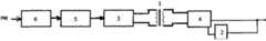
图1是本发明提供的IGBT驱动电路的结构框图;Fig. 1 is the structural block diagram of the IGBT driving circuit provided by the present invention;
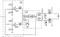
图2是本发明提供的充放电模块的电路结构示意图;2 is a schematic diagram of the circuit structure of the charging and discharging module provided by the present invention;
图3是本发明提供的尖脉冲产生模块的结构示意图;Fig. 3 is a schematic structural diagram of a spike generating module provided by the present invention;
图4是本发明提供的回复模块的结构示意图;Fig. 4 is a schematic structural diagram of a reply module provided by the present invention;
图5是本发明提供的窄脉冲抑制模块的结构示意图;Fig. 5 is a schematic structural diagram of a narrow pulse suppression module provided by the present invention;
图6是本发明提供的死区插入模块的结构示意图;Fig. 6 is a schematic structural diagram of a dead zone insertion module provided by the present invention;
图7是PWM波形、第一运算放大器输出信号的波形、第二运算放大器输出信号的波形、充电时序信号的波形以及放电时序信号的波形的时序图;7 is a timing diagram of a PWM waveform, a waveform of an output signal of a first operational amplifier, a waveform of an output signal of a second operational amplifier, a waveform of a charging timing signal, and a waveform of a discharging timing signal;
图8是应用于电动车电机的IGBT驱动电路的示意图。Fig. 8 is a schematic diagram of an IGBT driving circuit applied to an electric vehicle motor.
具体实施方式Detailed ways
下面结合附图对本发明作进一步的描述。The present invention will be further described below in conjunction with the accompanying drawings.
如图1所示,本发明提供一种IGBT驱动电路,该驱动电路包括:变压器1,该变压器1的初级侧用于接收PWM信号,其中,该驱动电路还包括充放电模块2,所述变压器1的次级侧用于连接绝缘栅双极型晶体管的栅极,并且与充放电模块2的输入端连接,充放电模块2的输出端用于与绝缘栅双极型晶体管的栅极相连接,该充放电模块2用于接收所述变压器1的次级侧输出的PWM信号,根据该PWM信号对所述绝缘栅双极型晶体管进行充电或放电以使得所述绝缘栅双极型晶体管在导通前被预充电和在关断前被预放电。As shown in Figure 1, the present invention provides an IGBT drive circuit, the drive circuit includes: a
其中,所述充放电模块2根据所述PWM信号生成充电时序信号和放电时序信号,并根据该充电时序信号和放电时序信号对所述绝缘栅双极型晶体管进行充电或放电,其中,在所述PWM信号的一个脉冲周期内,所述充电时序信号在PWM信号的电压从0V上升到峰值之前为有效电平,所述放电时序信号在所述PWM信号从峰值下降到0V之前为有效电平。一般采用高电平作为有效电平。Wherein, the charging and
所述变压器1为本领域技术人员公知的脉冲变压器,所述变压器1的初级侧和次级侧的线圈匝数比可以为任意,优选为1∶1。The
如图2所示,所述充放电模块2包括比较单元21、时序逻辑单元22、充电单元23和放电单元24,所述比较单元21的输入端与所述变压器1的次级侧连接,比较单元21的第一输出端和第二输出端分别与时序逻辑单元22的第一信号输入端和第二信号输入端连接,时序逻辑单元22的第一信号输出端和第二信号输出端分别与充电单元23和放电单元24的控制端连接。As shown in Figure 2, the charging and
其中,所述比较单元21用于接收所述变压器1的次级侧输出的PWM信号,将该PWM信号的电压与设定的第一电压和第二电压进行比较,根据比较结果输出触发信号,其中0V<第一电压<第二电压<PWM信号的峰值电压。所述第一电压和第二电压介于使IGBT关断的有效电压(即0V)和使IGBT导通的有效电压(即PWM信号的峰值电压)之间。Wherein, the
其中,所述比较单元21可以采用本领域人员公知的比较电路,例如如图2所示,所述比较单元21包括第一运算放大器211、第一电阻212、第一稳压管213、第一二极管214、第二运算放大器215、第二电阻216、第二稳压管217和第二二极管218,所述第一运算放大器211的正相输入端、第二运算放大器215的正相输入端均与变压器1的次级侧连接,用于从所述变压器1的次级侧接收PWM信号,第一运算放大器211和第二运算放大器215的反相输入端分别通过第一电阻212和第二电阻216输入一正电压,并分别与第一稳压管213和第二稳压管217的阴极连接,所述第一稳压管213和第二稳压管217的阳极接地,所述第一运算放大器211和第二运算放大器215的输出端分别接第一二极管214和第二二极管218的阳极,第一二极管214和第二二极管218的阴极分别连接到所述时序逻辑单元22的第一信号输入端和第二信号输入端。Wherein, the
更具体地说,当PWM信号从第一运算放大器211和第二运算放大器215的正相输入端输入时,对PWM信号的每一个脉冲,在该脉冲从0上升到峰值以及由峰值下降到0的整个过程中,如果输入的电压大于第一稳压管213的击穿后的端电压(以下简称端电压)(即第一电压),则第一运算放大器211的输出端输出高电平,如果输入的电压低于第一稳压管213的端电压,则第一运算放大器211的输出端输出低电平;对于第二稳压管217和第二运算放大器215也具有与第一稳压管213和第一运算放大器211相同的原理,不多做描述。第一稳压管213和第二稳压管217的端电压(即第一电压和第二电压)被设置为不同,第一稳压管213端电压小于第二稳压管217,例如,PWM信号高电平为15v,第一稳压管213的端电压为5v,第二稳压管217的端电压为14v,则在输入PWM信号后得到第一运算放大器211的输出端和第二运算放大器215的输出端输出的信号的时序波形如图7所示,波形A是PWM信号的波形,黑点处例如分别为5v和14v电压,波形B是第一运算放大器211输出端输出的信号的波形,波形C是第二运算放大器215输出端输出的信号的波形。根据不同的IGBT导通电压和关断电压的不同以及需要对其充放电的时间的不同,所述第一稳压管213和第二稳压管217的端电压可以在0到PWM信号高电平的电压之间设置。More specifically, when the PWM signal is input from the non-inverting input terminals of the first
所述第一稳压管213和第二稳压管217可以是齐纳二极管。The first voltage regulator tube 213 and the second
所述时序逻辑单元22用于接收所述触发信号,根据该触发信号中的上升沿生成所述充电时序信号,根据下降沿生成所述放电时序信号,并分别通过第一信号输出端和第二信号输出端输出。The
所述时序逻辑单元22根据第一运算放大器211输出的信号和第二运算放大器215输出的信号来在特定的时间段分别使第一信号输出端和第二信号输出端输出信号。也就是说,如图7所示,在PWM信号的一个脉冲周期中,从第一运算放大器211输出的信号(波形B)由低电平变到高电平的时刻t1起到第二运算放大器215输出的信号由低电平变到高电平的时刻t2所经过的时间段,所述第一信号输出端输出有效信号(高电平信号);从第二运算放大器215输出的信号由高电平变到低电平的时刻t3起到第一运算放大器211输出的信号由高电平变到低电平的时刻t4所经过的时间段,所述第二信号输出端输出有效信号(高电平信号)。The
所述时序逻辑单元22可以通过边沿触发器来实现上述功能,例如可以采用上升沿触发的触发器和下降沿触发的触发器进行结合来实现时序逻辑单元22,上升沿触发的触发器接收一个上升沿触发信号,其输出的信号翻转(即由高电平变到低电平或由低电平变到高电平),下降沿触发的触发器具有类似功能,只是其触发信号是下降沿信号,这为本领域技术人员公知,不多做描述。The
如图2所示,所述时序逻辑单元22还可以通过单片机221或其它的处理单元并结合相应的程序来实现,该时序逻辑单元22可以包括单片机221、第一非门电路222和第二非门电路223,所述单片机221的第一信号输入端和第二信号输入端分别接比较单元21的第一输出端和第二输出端以接收触发信号(例如所述第一二极管214和第二二极管218的阴极),单片机221的两个信号输出端分别通过第一非门电路222和第二非门电路223接所述充电单元23和放电单元24的控制端。As shown in Figure 2, the
为单片机221预先编程,使单片机221实现如下功能:在PWM信号的每一个脉冲周期期间,当单片机221的第一信号输入端接收到一个上升沿触发信号时,单片机221的其中一个信号输出端通过第一非门电路222输出有效信号(高电平信号),当单片机221的第二信号输入端接收到一个上升沿触发信号时,通过第一非门电路222输出无效信号(即原输出的信号翻转,由高电平信号变为低电平信号),通过第一非门电路222输出的信号即为充电时序信号,其波形如图7中的波形E所示;单片机221的第二信号输入端接收一个下降沿触发信号,单片机221的另一个信号输出端通过第二非门电路223输出有效信号(高电平信号),单片机221的第一信号输入端再接收一个下降沿触发信号,通过第二非门电路223输出无效信号(即原输出的信号翻转,由高电平信号变为低电平信号),通过第二非门电路223输出的信号即为放电时序信号,其波形如图7中的波形F所示。The single-
优选情况下,单片机221可选为8脚单片机,例如P89LPC90x系列、PIC12C67X系列。如有需要,该单片机221可以接入晶体振荡器从而被提供时钟源。Preferably, the single-
所述充电单元23和放电单元24分别用于根据所述充电时序信号和放电时序信号对所述绝缘栅双极型晶体管进行充电和放电。The
所述充电单元23包括第一开关管,放电单元24包括第二开关管,第一开关管和第二开关管的控制端分别与所述第一非门电路222和第二非门电路223的输出端相连接,第一开关管的输入端接入一正电压,其输出端接所述绝缘栅双极型晶体管的栅极,所述第二开关管的输入端接绝缘栅双极型晶体管的栅极,第二开关管的输出端接入一负电压(或接地)。The
可以在所述第一开关管和第二开关管的控制端分别反向串接一稳压管,且该稳压管两端可以跨接一电阻,以起到稳定控制端的电压的作用;时序逻辑单元22的第一信号输出端和第二信号输出端(如第一非门电路222和第二非门电路223的输出端)分别通过上拉电阻接正电压。所述正电压和负电压可以分别通过直流稳压源来提供。A voltage regulator tube can be connected in reverse series at the control terminals of the first switch tube and the second switch tube respectively, and a resistor can be connected across the two ends of the voltage regulator tube to stabilize the voltage at the control terminal; The first signal output terminal and the second signal output terminal of the logic unit 22 (such as the output terminals of the first NOT gate circuit 222 and the second NOT gate circuit 223 ) are respectively connected to a positive voltage through a pull-up resistor. The positive voltage and the negative voltage can be respectively provided by a DC stabilized voltage source.
所述第一开关管和第二开关管可以是本领域技术人员公知的MOS管、继电器、三极管等,优选为MOS管;更优选的,第一开关管为N沟道MOS管,该N沟道MOS管的栅极、漏极和源极分别作为所述第一开关管的控制端、输入端和输出端;所述第二开关管为P沟道MOS管,该P沟道MOS管的栅极、漏极和源极分别作为所述第二开关管的控制端、输入端和输出端。The first switching tube and the second switching tube can be MOS tubes, relays, triodes, etc. known to those skilled in the art, preferably MOS tubes; more preferably, the first switching tube is an N-channel MOS tube, and the N-channel The gate, the drain and the source of the MOS transistor are respectively used as the control terminal, the input terminal and the output terminal of the first switch tube; the second switch tube is a P-channel MOS tube, and the P-channel MOS tube The gate, the drain and the source serve as the control terminal, the input terminal and the output terminal of the second switch tube respectively.
如图1所示,所述驱动电路还包括边沿尖脉冲产生模块3和回复模块4,边沿尖脉冲产生模块3的输出端接所述变压器1的初级侧,变压器1的次级侧接回复模块4的输入端,回复模块4的输出端接绝缘栅双极型晶体管的栅极和所述充放电模块2的输入端。该边沿尖脉冲产生模块3用于接收PWM信号,将PWM信号转变成尖脉冲信号,并将该尖脉冲信号输出到所述变压器1的初级侧;回复模块4用于将通过所述变压器1传输的经所述边沿尖脉冲产生模块3转变的尖脉冲信号回复成PWM信号并将该PWM信号输出到所述充放电模块2和绝缘栅双极型晶体管。As shown in Figure 1, the drive circuit also includes an edge
如图3所示,所述边沿尖脉冲产生模块3可以包括微分电路和绝对值电路34,所述微分电路包括第三运算放大器31、第三电阻32和第一电容33,所述第三运算放大器31的正相输入端接地,其负相输入端通过第一电容33接收PWM信号,并通过第三电阻32接第三运算放大器31的输出端,该输出端接所述绝对值电路34的输入端,绝对值电路34的输出端接所述变压器1的初级侧。As shown in Figure 3, the edge
微分电路可以提取输入的PWM信号的上升边沿和下降边沿,将其转变成尖脉冲信号,绝对值电路34将使上升沿和下降沿同相,利用边沿尖脉冲产生模块3转变后的尖脉冲去驱动上升变压器1,可以缩短变压器1工作的时间,因此可以采用功率小的变压器1,相应地能减小变压器1的体积。The differential circuit can extract the rising edge and falling edge of the input PWM signal and convert it into a spike signal. The
如图4所示,所述回复模块4包括触发器41和功率放大单元42,触发器41用于将所述变压器1输出的所述尖脉冲信号回复成PWM信号,并通过功率放大单元42放大后输出该PWM信号。变压器1次级侧输出的是尖脉冲信号,回复电路的触发器41可以将尖脉冲信号回复成PWM信号。触发器41可以采用双稳态触发器41,触发器41接收一个上升沿触发信号,其输出的信号就发生翻转(即高低电平翻转),这样就能将尖脉冲信号整形成PWM信号,再通过功率放大单元42放大后输出。所述触发器41和功率放大单元42为本领域技术人员所公知,不多做描述。As shown in FIG. 4 , the
在传统变压器1传输的过程中,小于500ns的脉冲几乎能量很小,通过变压器1传输失真后去驱动功率器件,功率器件很容易被损坏,因此有必要将这种窄脉冲抑制掉。一般的PWM信号中都混杂有这种脉冲,基于这一点,如图1所示,所述驱动电路还包括窄脉冲抑制模块5,窄脉冲抑制模块5的输出端与所述边沿尖脉冲产生模块3的输入端相连接,用于抑制PWM信号中的窄脉冲,该窄脉冲为小于500ns的脉冲。如图5所示,所述窄脉冲抑制模块5可以包括第四运算放大器51和RC网络52,第四运算放大器51的正相输入端接所述RC网络52并用于接收PWM信号,其负相输入端接地,第四运算放大器51的输出端通过所述第一电容33与所述第三运算放大器31的负相输入端连接。通过调节RC参数可以改变要抑制的脉冲宽度。所述RC网络52为本领域技术人员公知的RC滤波电路。During the transmission process of the
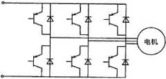
在IGBT的应用中,例如将IGBT应用到电动车的电机的控制电路中,电机的控制一般采用IGBT三相全桥电路,如图8所示,电机每一相所连接的上下桥臂的IGBT不能同时导通,为了保证每一相所连接的上下桥臂的IGBT错开导通与关断时间,必须在其中一个IGBT关断后延时一定的时间(死区时间)后另一个IGBT才导通,反之亦然。In the application of IGBT, for example, the IGBT is applied to the control circuit of the motor of the electric vehicle. The control of the motor generally adopts the IGBT three-phase full-bridge circuit. As shown in Figure 8, the IGBTs of the upper and lower bridge arms connected to each phase of the motor It cannot be turned on at the same time. In order to ensure the staggered turn-on and turn-off times of the IGBTs connected to the upper and lower bridge arms of each phase, the other IGBT must be turned on after a certain period of time (dead time) after one of the IGBTs is turned off. pass, and vice versa.
为在应用中实现上述目的,如图1所示,上述驱动电路还包括死区插入模块6,该死区插入模块6用于接收PWM信号,并将对该信号插入死区时间后再输出,例如输出到窄脉冲抑制模块5的输入端。如图6所示,该死区插入模块6包括第五运算放大器61和延时电路,所述第五运算放大器61的正相输入端用于接收PWM信号,第五运算放大器61的输出端用于输出延时的PWM信号,所述延时电路包括第一与非门电路62、第一可调电阻63、第二电容64、第二与非门电路65、第二可调电阻66和第三电容67,第一与非门电路62的第一输入端用于接收输入的PWM信号,并连接第一可调电阻63的一端,第一可调电阻63的另一端接第一与非门电路62的第二输入端并通过第二电容64接地,第一与非门电路62的输出端接第二与非门电路65的第一输入端和第二可调电阻66的一端,第二可调电阻66的另一端接第二与非门电路65的第二输入端并通过第三电容67接地,第二与非门电路65的输出端接第五运算放大器61的负相输入端。死区插入是将同一桥臂上下桥驱动波形插入一定的延时,让上下桥中的一个IGBT先关断一定的时间再导通另一个IGBT,以避免同时导通的可能造成串通的危险,通过第一与非门电路62、第一可调电阻63和第二电容64可以将输入的PWM信号的上升延延时,通过第二与非门电路65、第二可调电阻66和第三电容67可以将输入的PWM信号的下降沿延时,以插入死区时间,且死区时间可调,可以通过调节第一可调电阻63和第二电容64以及第二可调电阻66和第三电容67来调节死区时间。这为本领域技术人员所公知,不再详细描述。In order to achieve the above purpose in the application, as shown in Figure 1, the above-mentioned drive circuit also includes a dead
下面阐述本发明提供的IGBT驱动电路是如何减小导通时的di/dt和关断时的dv/dt的。The following describes how the IGBT drive circuit provided by the present invention reduces di/dt at turn-on and dv/dt at turn-off.
PWM信号传输到所述充放电模块2的第一运算放大器211和第二运算放大器215的正相输入端时,在每一个脉冲周期,由第一运算放大器211和第一稳压管213组成的比较器将输入的脉冲信号(如图7中波形A)的电压与第一稳压管213的端电压(第一电压)进行比较(例如5v),如果大于该端电压,则第一运算放大器211通过第一二极管214输出高电平信号,如果小于端电压,则输出低电平信号,则第一运算放大器211通过第一二极管214输出的信号的波形如图7中波形B所示。同理,第二运算放大器215通过第二二极管218输出的信号的波形如图7中波形C所示(第二稳压管217端电压(第二电压)比第一稳压管213的大,例如是14v)。单片机221根据接收到的信号作出如下控制操作:在每一个脉冲周期中,单片机221在接收到信号的第一个上升沿(波形B上升沿)时,单片机221输出信号使第一开关管导通,从而给IGBT充电,单片机221在接收到第二个上升沿时(波形C的上升沿),单片机221停止输出信号使第一开关管关断,停止给IGBT充电;单片机221在接收到信号的第一个下降沿(波形C的下降沿)时,单片机221输出信号使第二开关管导通,从而给IGBT放电,单片机221在接收到第二个下降沿时(波形B的下降沿),单片机221停止输出信号使第二开关管关断,停止给IGBT放电。可以看出,调节第一稳压管213和第二稳压管217之间的端电压差,就能调节两个上升沿或下降沿之间的时间差,从而能调节充放电时间。因为第一稳压管213的端电压(第一电压)和第二稳压管217的端电压(第二电压)介于使IGBT关断的有效电压和使IGBT导通的有效电压之间,所以上述的充放电过程都是在开启或关断IGBT之前,因此能有效地抑制导通时的di/dt和关断时的dv/dt。When the PWM signal is transmitted to the non-inverting input terminals of the first
Claims (10)
Translated fromChinesePriority Applications (1)
| Application Number | Priority Date | Filing Date | Title |
|---|---|---|---|
| CN2008101612226ACN101677240B (en) | 2008-09-18 | 2008-09-18 | Isolated gate bipolar transistor driving circuit |
Applications Claiming Priority (1)
| Application Number | Priority Date | Filing Date | Title |
|---|---|---|---|
| CN2008101612226ACN101677240B (en) | 2008-09-18 | 2008-09-18 | Isolated gate bipolar transistor driving circuit |
Publications (2)
| Publication Number | Publication Date |
|---|---|
| CN101677240A CN101677240A (en) | 2010-03-24 |
| CN101677240Btrue CN101677240B (en) | 2012-01-25 |
Family
ID=42029671
Family Applications (1)
| Application Number | Title | Priority Date | Filing Date |
|---|---|---|---|
| CN2008101612226AActiveCN101677240B (en) | 2008-09-18 | 2008-09-18 | Isolated gate bipolar transistor driving circuit |
Country Status (1)
| Country | Link |
|---|---|
| CN (1) | CN101677240B (en) |
Families Citing this family (11)
| Publication number | Priority date | Publication date | Assignee | Title |
|---|---|---|---|---|
| CN101867174B (en)* | 2010-06-07 | 2013-04-24 | 大连海事大学 | IGBT short-circuit protection circuit in frequency converter and method thereof |
| CN103326706B (en)* | 2013-05-27 | 2015-12-23 | 上海奔赛电子科技发展有限公司 | A kind of filter circuit of integrated circuit and integrated circuit |
| CN103346759B (en)* | 2013-07-23 | 2016-01-13 | 郁百超 | Micro-power-consumptpower power frequency pulse width modulation switch power source |
| CN103944372B (en)* | 2014-04-11 | 2016-06-15 | 广东明阳龙源电力电子有限公司 | A kind of IGBT Drive Protecting Circuit |
| US9685947B2 (en) | 2015-03-30 | 2017-06-20 | Halliburton Energy Services, Inc. | Simplified gate driver for power transistors |
| US9692409B2 (en) | 2015-03-30 | 2017-06-27 | Halliburton Energy Services, Inc. | Simplified gate driver for power transistors |
| CN104967349A (en)* | 2015-06-23 | 2015-10-07 | 四川蜀旺科技有限公司 | Circuit capable of reducing loss of switch transistor and driving schedule method |
| CN109450418B (en)* | 2018-11-12 | 2024-02-23 | 成都法姆科技有限公司 | IGBT isolation driving circuit with switch control unit and control method thereof |
| CN110421244B (en)* | 2019-08-27 | 2024-06-25 | 无锡海菲焊接设备有限公司 | Welding control system of energy storage welding machine |
| CN115334713B (en)* | 2022-08-25 | 2025-04-11 | 苏州中科华矽半导体科技有限公司 | LED driving circuit and control method |
| CN117526916B (en)* | 2023-12-29 | 2024-04-05 | 珠海格力电器股份有限公司 | Driving circuit and method for insulated gate bipolar transistor |
Citations (2)
| Publication number | Priority date | Publication date | Assignee | Title |
|---|---|---|---|---|
| CN1136730A (en)* | 1995-04-05 | 1996-11-27 | 精工电子工业株式会社 | Reference voltage semiconductor device |
| US5929368A (en)* | 1996-12-09 | 1999-07-27 | The Ensign-Bickford Company | Hybrid electronic detonator delay circuit assembly |
- 2008
- 2008-09-18CNCN2008101612226Apatent/CN101677240B/enactiveActive
Patent Citations (2)
| Publication number | Priority date | Publication date | Assignee | Title |
|---|---|---|---|---|
| CN1136730A (en)* | 1995-04-05 | 1996-11-27 | 精工电子工业株式会社 | Reference voltage semiconductor device |
| US5929368A (en)* | 1996-12-09 | 1999-07-27 | The Ensign-Bickford Company | Hybrid electronic detonator delay circuit assembly |
Also Published As
| Publication number | Publication date |
|---|---|
| CN101677240A (en) | 2010-03-24 |
Similar Documents
| Publication | Publication Date | Title |
|---|---|---|
| CN101677240B (en) | Isolated gate bipolar transistor driving circuit | |
| US10340906B2 (en) | Integrated bootstrap high-voltage driver chip and technological structure thereof | |
| CN104025454B (en) | Semiconductor device and the driving method of high lateral circuit | |
| JP2585284B2 (en) | Power MOSFET gate drive circuit | |
| TWI418146B (en) | Floating driving circuit | |
| US20140063593A1 (en) | Capacitor discharge pulse drive circuit with fast recovery | |
| EP3621202A1 (en) | Adaptive multi-level gate driver | |
| CN103326706B (en) | A kind of filter circuit of integrated circuit and integrated circuit | |
| CN102148614B (en) | Pulse-generating circuit and method, reference voltage produce and promote circuit and method | |
| CN202524281U (en) | Isolated rapid turn-off oxide field effect transistor (MOFET) driving circuit | |
| CN105007062B (en) | A kind of SPM high reliability edge pulse-generating circuit | |
| CN110620573B (en) | Driving circuit of power semiconductor switch | |
| CN106849621A (en) | A kind of system and method for realizing gate driving circuit | |
| CN111555595B (en) | GaN power tube gate drive circuit with controllable opening rate | |
| CN110943722B (en) | Driving circuit | |
| CN108649936A (en) | A kind of pulsewidth modulation of Magnetic isolation driving and demodulator circuit | |
| CN104796098A (en) | GaN power device drain electrode modulation circuit | |
| CN102158207A (en) | Impulse modulation method and circuit for switch transistor drive signals | |
| CN104811174A (en) | Power switch tube driving circuit capable of regulating switching speed of power switch tube | |
| CN103825434B (en) | A kind of IGBT drive circuit | |
| CN118074684B (en) | High-voltage integrated circuit with minimum pulse width regulating function | |
| CN108566185B (en) | Power tube driving circuit and driver | |
| CN109240408A (en) | SiCMOSFET gate drive voltage control circuit and its control method | |
| CN204794929U (en) | Intelligence power module high reliability border pulse -generating circuit | |
| CN119030516A (en) | A MOSFET drive signal generating circuit with adjustable pulse width and frequency |
Legal Events
| Date | Code | Title | Description |
|---|---|---|---|
| C06 | Publication | ||
| PB01 | Publication | ||
| C10 | Entry into substantive examination | ||
| SE01 | Entry into force of request for substantive examination | ||
| C14 | Grant of patent or utility model | ||
| GR01 | Patent grant | ||
| TR01 | Transfer of patent right | Effective date of registration:20240105 Address after:231400 No. 1, Zone B, Shuangchuang Industrial Park, Tongcheng Economic and Technological Development Zone, Anqing City, Anhui Province Patentee after:Haozhi Technology Electric Drive (Tongcheng) Co.,Ltd. Address before:518118, Ping Ping Road, Pingshan Town, Longgang District, Guangdong, Shenzhen 3001 Patentee before:BYD Co.,Ltd. | |
| TR01 | Transfer of patent right |