CN101675536B - Led module with colour conversion layer designed for a homogenous colour distribution - Google Patents
Led module with colour conversion layer designed for a homogenous colour distributionDownload PDFInfo
- Publication number
- CN101675536B CN101675536BCN2008800140692ACN200880014069ACN101675536BCN 101675536 BCN101675536 BCN 101675536BCN 2008800140692 ACN2008800140692 ACN 2008800140692ACN 200880014069 ACN200880014069 ACN 200880014069ACN 101675536 BCN101675536 BCN 101675536B
- Authority
- CN
- China
- Prior art keywords
- color conversion
- color
- led module
- conversion layer
- vol
- Prior art date
- Legal status (The legal status is an assumption and is not a legal conclusion. Google has not performed a legal analysis and makes no representation as to the accuracy of the status listed.)
- Expired - Fee Related
Links
- 238000006243chemical reactionMethods0.000titleclaimsabstractdescription100
- 239000000126substanceSubstances0.000claimsdescription36
- 238000000034methodMethods0.000claimsdescription17
- 238000004519manufacturing processMethods0.000claimsdescription12
- 239000002245particleSubstances0.000claimsdescription8
- 230000000737periodic effectEffects0.000claimsdescription8
- 239000011888foilSubstances0.000claimsdescription2
- 239000000463materialSubstances0.000claimsdescription2
- 239000010410layerSubstances0.000description102
- OAICVXFJPJFONN-UHFFFAOYSA-NPhosphorusChemical compound[P]OAICVXFJPJFONN-UHFFFAOYSA-N0.000description13
- 239000004065semiconductorSubstances0.000description13
- 229910052594sapphireInorganic materials0.000description8
- 239000010980sapphireSubstances0.000description8
- 230000005855radiationEffects0.000description5
- 238000001228spectrumMethods0.000description5
- 239000011159matrix materialSubstances0.000description4
- 239000000758substrateSubstances0.000description4
- 239000012780transparent materialSubstances0.000description4
- 230000002596correlated effectEffects0.000description2
- 239000013078crystalSubstances0.000description2
- 238000010521absorption reactionMethods0.000description1
- 239000012790adhesive layerSubstances0.000description1
- 239000011248coating agentSubstances0.000description1
- 238000000576coating methodMethods0.000description1
- 230000000875corresponding effectEffects0.000description1
- 230000001186cumulative effectEffects0.000description1
- 230000001419dependent effectEffects0.000description1
- 238000010586diagramMethods0.000description1
- 230000000694effectsEffects0.000description1
- 238000000295emission spectrumMethods0.000description1
- 230000005284excitationEffects0.000description1
- 238000000695excitation spectrumMethods0.000description1
- 238000000605extractionMethods0.000description1
- 239000003292glueSubstances0.000description1
- 239000011229interlayerSubstances0.000description1
- 238000004020luminiscence typeMethods0.000description1
- 229920000642polymerPolymers0.000description1
- 239000000843powderSubstances0.000description1
- 238000002310reflectometryMethods0.000description1
- 239000011347resinSubstances0.000description1
- 229920005989resinPolymers0.000description1
- 238000004088simulationMethods0.000description1
- 239000002356single layerSubstances0.000description1
- 239000006104solid solutionSubstances0.000description1
Images


Classifications
- H—ELECTRICITY
- H10—SEMICONDUCTOR DEVICES; ELECTRIC SOLID-STATE DEVICES NOT OTHERWISE PROVIDED FOR
- H10H—INORGANIC LIGHT-EMITTING SEMICONDUCTOR DEVICES HAVING POTENTIAL BARRIERS
- H10H20/00—Individual inorganic light-emitting semiconductor devices having potential barriers, e.g. light-emitting diodes [LED]
- H10H20/80—Constructional details
- H10H20/85—Packages
- H10H20/851—Wavelength conversion means
- H10H20/8514—Wavelength conversion means characterised by their shape, e.g. plate or foil
Landscapes
- Led Device Packages (AREA)
- Led Devices (AREA)
Abstract
Translated fromChineseDescription
Translated fromChinese技术领域technical field
本发明涉及使用以下将称为LED的半导体器件来产生光的领域。本发明对于通过使LED发射具有第一光谱的光并将该光与通过部分地转换具有第一光谱的光而产生的第二光谱相混合特别有用。以下将这种转换称为颜色转换。The present invention relates to the field of light generation using semiconductor devices which will be referred to hereinafter as LEDs. The invention is particularly useful by having an LED emit light having a first spectrum and mixing this light with a second spectrum produced by partially converting the light having the first spectrum. This conversion is hereinafter referred to as color conversion.
背景技术Background technique
发出的(混合的)光的颜色显然取决于转换后的光与具有原始第一光谱的光的比率。该比率进而取决于当具有第一光谱的光传播通过颜色转换层时的有效路径长度。对于不同的发射角而言,有效路径长度可能不同,这导致了当查看由LED模块照亮的远场模式的角分布(angulardistribution)时的不均匀的色温。有效路径长度还取决于各辐射模式的叠加,对于源自半导体发射器的光(接近朗博形状(lambertian shape))和转换后的光(各向同性发光,isotropic luminescence)而言,辐射模式是不同的。最常规类型的LED的颜色变化其自身通常表现为,在光束中,中间是较冷色的白色,而离轴处是较暖色的白色或淡黄色的环。这暗示了颜色转换层的几何形状是LED模块的色温的均匀性的因素。The color of the emitted (mixed) light obviously depends on the ratio of converted light to light with the original first spectrum. This ratio in turn depends on the effective path length when light having the first spectrum propagates through the color conversion layer. The effective path length may be different for different emission angles, which leads to a non-uniform color temperature when looking at the angular distribution of the far-field pattern illuminated by the LED module. The effective path length also depends on the superposition of the radiation modes, which for the light originating from the semiconductor emitter (approximate lambertian shape) and the converted light (isotropic luminescence) are different. The color change of the most conventional types of LEDs usually manifests itself as a ring of cooler white in the center and warmer white or yellowish off-axis in the beam. This implies that the geometry of the color conversion layer is a factor for the uniformity of the color temperature of the LED module.
已知一种在LED芯片上的颜色转换层的在几何形状上明确限定的(所谓“保形(conformal)”)涂层改善了色温的角均匀性。A geometrically well-defined (so-called "conformal") coating of the color conversion layer on the LED chip is known to improve the angular uniformity of the color temperature.
US 6,650,044致力于一种在倒装式几何形状上形成大致保形的涂层的荧光粉层的结构的器件和制造方法(刻版印花法(stenciling)),该结构具有大致均匀的厚度,其表面基本上与倒装式LED的侧平面平行。US 6,650,044 is directed to a device and method of manufacture (stenciling) of a structure forming a substantially conformal coated phosphor layer on a flip-chip geometry, the structure having a substantially uniform thickness, its The surface is substantially parallel to the side planes of the flip-chip LED.
US 6,642,652提出了一种LED器件,该LED器件由在顶面上具有大致恒定的厚度(厚度最多偏差平均值10%)并与半导体叠层的边相邻的荧光粉转换层(单层或多层)均匀地覆盖。与裸LED相比,转换层未显著地增加源的尺寸。该器件限于LED并且对基台(submount)或反射器或PCB覆盖不超过100μm。US 6,642,652 proposes an LED device consisting of a phosphor conversion layer (single or multiple layer) to cover evenly. The conversion layer does not significantly increase the size of the source compared to bare LEDs. The device is limited to LEDs and covers no more than 100 μm to the submount or reflector or PCB.
US 7,078,732提出了一种直接地设置在半导体主体上的颜色转换层,并且示出了整体上大体恒定的层厚度。在该现有技术文献的图3中,颜色转换层被示出为设置在壳体的顶部,在该壳体中的凹部中设置有LED芯片。以透明材料填充未用的空间。转换层具有大致恒定的厚度并且超过了LED芯片的有源区(active region)。然而,在该示例中,该层没有直接地设置在半导体上。US 7,078,732 proposes a color conversion layer arranged directly on the semiconductor body and shows a substantially constant layer thickness overall. In Fig. 3 of this prior art document, the color converting layer is shown arranged on top of a housing in which the LED chips are arranged in recesses. Fill unused space with transparent material. The conversion layer has an approximately constant thickness and extends beyond the active region of the LED chip. However, in this example, this layer is not disposed directly on the semiconductor.
US申请2006/0071223教导了一种颜色转换层,该颜色转换层被特意构造成在所有的视角实现均匀的颜色空间。该结构被描述成具有周期性变化的厚度或凹进区(在芯片的边缘处)。US application 2006/0071223 teaches a color conversion layer that is deliberately structured to achieve a uniform color space at all viewing angles. The structure is described as having periodically varying thickness or recessed regions (at the edge of the chip).
US 6,963,166示出了一种LED灯,该LED灯具有覆盖了倒装式LED的至少一个侧表面的树脂部(转换层),并具有与用于获得期望的角均匀性所需侧表面分开的弯曲反射器。US 6,963,166 shows an LED lamp having a resin portion (conversion layer) covering at least one side surface of a flip-chip LED and having a Curved reflector.
US 6,635,363示出了一种具有荧光粉层的LED,该荧光粉层的厚度与其下面的LED所发出的辐射的强度成比例,从而改善发出的辐射的均匀性。US 6,635,363 shows an LED with a phosphor layer whose thickness is proportional to the intensity of the radiation emitted by the LED below it, thereby improving the uniformity of the emitted radiation.
发明内容Contents of the invention
本发明的目的是提出一种明确地定义的最优颜色转换层,该颜色转换层促进了LED模块的均匀颜色分布。The object of the present invention is to propose a well-defined optimal color conversion layer which promotes a homogeneous color distribution of the LED module.
该目的是借助于独立权利要求的特征来实现。从属权利要求进一步发展了本发明的中心思想。This object is achieved by means of the features of the independent claims. The dependent claims further develop the central idea of the invention.
本发明已经发现,为了实现均匀的颜色分布,颜色转换层的某些尺寸是有利的,而且通过根据颜色转换物质的浓度和/或颜色转换颗粒的平均尺寸来调整颜色转换层的尺寸,可以进一步改善该效果。The present inventors have found that certain dimensions of the color converting layer are advantageous in order to achieve a uniform color distribution, and that by adjusting the size of the color converting layer according to the concentration of the color converting substance and/or the average size of the color converting particles, further Improve this effect.
本发明提出了一种LED模块,该LED模块包括:LED芯片,其包括位于基板上的半导体层结构,所述的层结构具有有源发光区;以及颜色转换层,其用于把从LED芯片发出的光的波长转换成第二波长,其中,颜色转换层具有基本均匀的厚度h并且在发光层的各个边上都横向地延伸出所述有源发光区之外一个非零的长度x,其中,x小于h。The present invention proposes an LED module, which includes: an LED chip, which includes a semiconductor layer structure on a substrate, and the layer structure has an active light-emitting area; and a color conversion layer, which is used to transform the LED chip wavelength conversion of emitted light to a second wavelength, wherein the color conversion layer has a substantially uniform thickness h and extends laterally on each side of the light emitting layer beyond said active light emitting region by a non-zero length x, Among them, x is smaller than h.
所述LED芯片的指向所述颜色转换层的表面可设置有通常呈微米级垂直尺寸的周期性或非周期性微型结构。The surface of the LED chip directed towards the color conversion layer may be provided with periodic or non-periodic microstructures, typically with vertical dimensions in the order of micrometers.
所述颜色转换层的指向远离所述LED芯片的表面可在所述颜色转换层的超出所述LED芯片的发光层的部分中和/或在所述颜色转换层与所述LED芯片的发光层相交迭的部分中设置有周期性或非周期性微型结构。同样地,这些微型结构可具有一般是微米级的垂直尺寸。The surface of the color conversion layer pointing away from the LED chip may be in a portion of the color conversion layer that extends beyond the light emitting layer of the LED chip and/or between the color conversion layer and the light emitting layer of the LED chip. Periodic or non-periodic microstructures are arranged in the overlapping parts. Likewise, these microstructures can have vertical dimensions that are typically on the order of microns.
所述颜色转换层还可以至少部分地覆盖所述LED芯片的侧面,其中,在所述LED芯片的所述侧面处的所述颜色转换层厚度d小于所述颜色转换层的高度h。The color conversion layer may also at least partially cover side faces of the LED chip, wherein the color conversion layer thickness d at the side faces of the LED chip is smaller than the color conversion layer height h.
本发明还适用于被构造为在所述LED半导体芯片的表面与所述颜色转换层之间具有薄且大致透明的中间层(例如,胶层)的LED器件。本发明还适用于其中该中间层充当散射层的LED器件。The invention is also applicable to LED devices configured with a thin and substantially transparent intermediate layer (eg glue layer) between the surface of the LED semiconductor chip and the color converting layer. The invention is also applicable to LED devices in which the interlayer acts as a scattering layer.
比率d/h可以在0.001和0.99之间进行选择,优选地在0.007和0.67之间选择。The ratio d/h can be chosen between 0.001 and 0.99, preferably between 0.007 and 0.67.
所述高度h可以在50μm和1000μm之间,优选的在100μm和800μm之间。Said height h may be between 50 μm and 1000 μm, preferably between 100 μm and 800 μm.
所述颜色转换层中的颜色转换物质的浓度可以在2vol%和50vol%之间进行选择,优选地在4vol%到40vol%之间选择。The concentration of the color conversion substance in the color conversion layer can be chosen between 2 vol % and 50 vol %, preferably between 4 vol % and 40 vol %.
参数x可以在1μm和300μm之间进行选择,优选地在5μm和150μm进行选择。The parameter x can be chosen between 1 μm and 300 μm, preferably between 5 μm and 150 μm.
所述颜色转换颗粒的粒径的d50(平均直径)值可以是在1μm和50μm之间,优选地在2μm和25μm之间。The d50 (average diameter) value of the particle size of the color converting particles may be between 1 μm and 50 μm, preferably between 2 μm and 25 μm.
本发明还发现,所述比率h/x对所述LED模块的均匀颜色分布起到一定作用:所述比率x可以是在1.01和1000之间,优选地不大于160。The invention has also found that said ratio h/x plays a role in the uniform color distribution of said LED module: said ratio x can be between 1.01 and 1000, preferably not more than 160.
对于全部颜色转换层材料的颜色转换物质的浓度介于5vol%和20vol%之间的情况而言,所述比率h/x可以在1.5和140之间。The ratio h/x can be between 1.5 and 140 for a concentration of color-converting substance of the total color-converting layer material between 5 vol % and 20 vol %.
本发明还发现,h与所述颜色转换层中的颜色转换物质的浓度c的比率对均匀的颜色分布起一定作用,并且所述比率可以在1和500之间进行选择,优选地在2.5和200μm/vol%之间选择。The present invention has also found that the ratio of h to the concentration c of the color-converting substance in the color-converting layer plays a role in the uniform color distribution, and that said ratio can be selected between 1 and 500, preferably between 2.5 and Choose between 200μm/vol%.
本发明还发现,x与所述颜色转换层中的颜色转换物质的浓度c的比率对均匀的颜色分布起一定作用,并且该比率可以在0.02与150之间进行选择,优选地在0.125μm/vol%与37.5μm/vol%之间选择。The present invention has also found that the ratio of x to the concentration c of the color conversion substance in the color conversion layer plays a role in the uniform color distribution, and this ratio can be selected between 0.02 and 150, preferably at 0.125 μm/ Choose between vol% and 37.5μm/vol%.
可以将颜色转换层设置成预制的箔片部件。The color conversion layer can be provided as a prefabricated foil part.
可以将所述颜色转换层直接地或间接地(即,利用其它元件(粘合层等))设置在所述LED芯片的顶面上。The color conversion layer may be disposed directly or indirectly (ie, with other elements (adhesive layer, etc.)) on the top surface of the LED chip.
所述颜色转换层可以是粘接或固定到所述LED芯片的所述顶面上的预制部件。The color conversion layer may be a prefabricated part glued or fixed to the top surface of the LED chip.
所述颜色转换层可以直接地设置在所述LED芯片的所述顶面上。The color conversion layer may be directly disposed on the top surface of the LED chip.
本发明的另一个方面涉及一种改善白光LED模块的颜色分布的均匀性的方法,该LED模块包括位于LED半导体芯片顶部的颜色转换层,该方法包括以下步骤:设置颜色转换层;设定所述颜色转换层的高度h;以及根据所述颜色转换层的高度来调整该层的宽度x和颜色转换物质的浓度c。Another aspect of the present invention relates to a method for improving the uniformity of color distribution of a white LED module comprising a color conversion layer on top of an LED semiconductor chip, the method comprising the steps of: providing the color conversion layer; setting the color conversion layer; The height h of the color conversion layer; and the width x of the layer and the concentration c of the color conversion substance are adjusted according to the height of the color conversion layer.
该方法可包括以下步骤:将h与所述颜色转换层中的所述颜色转换物质的浓度c的比率设定成1和500之间的值,优选地在2.5μm/vol%和200μm/vol%之间;以及将h与该层的延伸部的宽度x的比率设定成1.01和1000之间的值,优选地不大于160。The method may comprise the step of setting the ratio of h to the concentration c of said color converting substance in said color converting layer to a value between 1 and 500, preferably between 2.5 μm/vol % and 200 μm/vol %; and setting the ratio of h to the width x of the extension of the layer to a value between 1.01 and 1000, preferably not greater than 160.
本发明的另一个方面涉及一种制造大致发出白光的LED器件,所述白光具有期望的相关色温以及得到改善的颜色分布均匀性,该LED器件包括位于LED半导体芯片顶部的颜色转换层,所述颜色转换层在各边处都横向地延伸出所述LED芯片的有源发光表面一个距离x,该方法包括以下步骤:设置颜色转换层;设定所述颜色转换层的所述横向延伸x;以及根据该层的值x来调整该层的高度h和颜色转换物质的浓度c。Another aspect of the present invention relates to the manufacture of an LED device emitting substantially white light with a desired correlated color temperature and improved color distribution uniformity, the LED device comprising a color conversion layer on top of an LED semiconductor chip, the LED device comprising The color conversion layer extends laterally at each side by a distance x beyond the active light-emitting surface of the LED chip, the method comprising the steps of: arranging the color conversion layer; setting the lateral extension x of the color conversion layer; And the height h of the layer and the concentration c of the color converting substance are adjusted according to the value x of the layer.
该方法可包括以下步骤:将x与所述颜色转换层中的所述颜色转换物质的浓度c的比率设定成0.02和150之间的值,优选地在0.125μm/vol%和37.5μm/vol%之间;以及将h与所述层的所述延伸部的宽度x的比率设定成成1.01和1000之间的值,优选地不大于160。The method may comprise the step of setting the ratio of x to the concentration c of said color-converting substance in said color-converting layer to a value between 0.02 and 150, preferably between 0.125 μm/vol % and 37.5 μm/vol % between vol %; and setting the ratio of h to the width x of said extension of said layer to a value between 1.01 and 1000, preferably not greater than 160.
本发明的另一个方面涉及一种制造大致发出白光的LED器件,所述白光具有期望的相关色温以及得到改善的颜色分布均匀性,该LED器件包括位于LED半导体芯片顶部的颜色转换层,该方法包括以下步骤:设置包括浓度为c的颜色转换物质的颜色转换层;以及根据该浓度c的值来调整该层的高度h和所述颜色转换层的延伸部的宽度x。Another aspect of the present invention relates to a method of fabricating an LED device emitting substantially white light with a desired correlated color temperature and improved uniformity of color distribution, the LED device comprising a color converting layer on top of an LED semiconductor chip, the method The method comprises the steps of: providing a color conversion layer comprising a color conversion substance having a concentration c; and adjusting the height h of the layer and the width x of the extension of the color conversion layer according to the value of the concentration c.
该方法可包括以下步骤:将x与所述颜色转换层中的所述颜色转换物质的浓度c的比率设定成0.02和150之间的值,优选地在0.125μm/vol%和37.5μm/vol%之间;并且将h与所述颜色转换层中的所述颜色转换物质的浓度c的比率设定成1和500之间的值,优选地在2.5μm/vol%和200μm/vol%之间。The method may comprise the step of setting the ratio of x to the concentration c of said color-converting substance in said color-converting layer to a value between 0.02 and 150, preferably between 0.125 μm/vol % and 37.5 μm/vol % between vol%; and setting the ratio of h to the concentration c of said color-converting substance in said color-converting layer to a value between 1 and 500, preferably between 2.5 μm/vol% and 200 μm/vol% between.
附图说明Description of drawings
将结合附图通过以下本发明的优选实施方式的详细描述来说明本发明的其它目的、方面和优点。Other objects, aspects and advantages of the present invention will be illustrated through the following detailed description of preferred embodiments of the present invention in conjunction with the accompanying drawings.
图1示出了根据本发明的LED模块,其中,LED芯片面朝上安装,Fig. 1 shows an LED module according to the present invention, wherein the LED chips are mounted face-up,
图2示出了根据本发明的LED模块,其中,LED芯片面朝下安装(倒装式),Fig. 2 shows an LED module according to the present invention, wherein the LED chips are mounted face down (flip-chip),
图3示出了针对恒定总层宽b为1040μm(对于有源层宽度为940μm的芯片而言,x=50μm)和荧光粉浓度为10%vol.、以及不同的层厚度(a)100μm、(b)200μm、(c)400μm(最优)、(d)600μm、以及(e)700μm的情况下的平均色度坐标x’。此处:x=0.5*(b-940μm),Figure 3 shows for a constant total layer width b of 1040 μm (x=50 μm for a chip with an active layer width of 940 μm) and a phosphor concentration of 10% vol., and for different layer thicknesses (a) 100 μm, Average chromaticity coordinates x′ in the cases of (b) 200 μm, (c) 400 μm (optimum), (d) 600 μm, and (e) 700 μm. Here: x=0.5*(b-940μm),
图4示出了在上部具有半球形检测器的仿真模型中使用的远场的概略图,Figure 4 shows a schematic diagram of the far field used in the simulation model with a hemispherical detector in the upper part,
图5示出了针对根据图3(c)中最优的三个参数(层厚度h=400μm、总的层宽度1040μm(x=50μm)以及荧光粉浓度10%vol.;x=0.5*(b-940μm))的色度坐标x’的轮廓曲线图。Fig. 5 shows for three optimal parameters according to Fig. 3 (c) (layer thickness h=400 μ m, total layer width 1040 μ m (x=50 μ m) and
具体实施方式Detailed ways
本发明可应用于例如a)切割好的薄GaN表面发射LED芯片,以及b)使用蓝宝石基板(或具有大致相同的反射率的类似透明材料)并在LED的底部具有发射(GaN等)层的切割好的倒装式LED。The invention can be applied, for example, to a) diced thin GaN surface-emitting LED chips, and b) using a sapphire substrate (or similar transparent material with approximately the same reflectivity) and having an emitting (GaN, etc.) layer at the bottom of the LED Cut the flip-chip LED.
切割好的LED芯片的形状可以呈正方形或矩形。The shape of the cut LED chips can be square or rectangular.
根据本发明的颜色转换层包括位于对可见辐射透明的支撑基体(supportive matrix)(例如聚合物基体)中的发光颗粒(粉末或小的晶体)、荧光粉或“颜色转换物质”。The color conversion layer according to the invention comprises luminescent particles (powders or small crystals), phosphors or "color conversion substances" in a supporting matrix transparent to visible radiation, eg a polymer matrix.
本发明也可应用于包含有均匀地分散(即,在支撑基体中形成发光体分子的“固溶体”)的分子发光体的颜色转换层。The invention is also applicable to color conversion layers comprising molecular emitters dispersed homogeneously (ie forming a "solid solution" of emitter molecules in a support matrix).
本发明提出了具有超出了“中心层”之外的横向“延伸部”的颜色转换层,其中,中心层覆盖了半导体结构的有源发光层,该有源发光层是提供了光的外部耦合(outcoupling)并在LED芯片的顶面上限定的区域(在倒装式几何形状的情况下,光主要耦合到透明基板)。The present invention proposes a color conversion layer with a lateral "extension" beyond a "central layer", wherein the central layer covers the active light-emitting layer of the semiconductor structure which provides the outcoupling of light (outcoupling) and the area defined on the top surface of the LED chip (in the case of flip-chip geometry, the light is mainly coupled to the transparent substrate).
根据本发明,荧光粉转换层(phosphor conversion layer)设置在发光半导体结构与外部环境或次级光学元件之间,该荧光粉转换层超出半导体管芯(semiconductor die)的有源区域的几何形状之外的延伸部在正方形或矩形LED芯片的所有的4个边中都具有长度为x和高度为h的大致矩形的剖面。According to the invention, a phosphor conversion layer is arranged between the light-emitting semiconductor structure and the external environment or secondary optics, which phosphor conversion layer extends beyond the geometry of the active area of the semiconductor die. The outer extension has an approximately rectangular cross-section of length x and height h in all 4 sides of the square or rectangular LED chip.
转换层的覆盖了芯片的有源区域的中心部分优选地具有在整个有源发光区上大致不变的平均厚度,而且该平均厚度与延伸部的高度h类似。优选地,该平均厚度等于h。The central part of the conversion layer covering the active area of the chip preferably has an average thickness that is substantially constant over the entire active light-emitting area and that is similar to the height h of the extension. Preferably, this average thickness is equal to h.
然而,由于(i)LED芯片的表面可能含有微型结构(例如,棱锥(pyramid))以更好地从半导体层提取光,并且(ii)中心层的表面可能含有微型结构(与芯片表面的微型结构不同),因此中心部分的底面和顶面不一定是平行的。在肉眼可见的水平(macroscopic level)上,中心部分的底面和顶面优选地平行。However, since (i) the surface of the LED chip may contain microstructures (for example, pyramids) to better extract light from the semiconductor layer, and (ii) the surface of the center layer may contain microstructures (different from the microstructures on the chip surface), structure), so the bottom and top surfaces of the central part are not necessarily parallel. On a macroscopic level, the bottom surface and the top surface of the central part are preferably parallel.
将整个荧光粉转换层(即,中心层和延伸部)的形式选择成使得远场中的所有发射角上的颜色变化最小化。The form of the entire phosphor conversion layer (ie central layer and extensions) is chosen to minimize color variation over all emission angles in the far field.
在一个实施方式中,不管中心层的形状如何,延伸部的表面可大致是平面。具体地说,延伸部的表面可以是具有大致平行的平面的层。In one embodiment, regardless of the shape of the central layer, the surface of the extension may be substantially planar. Specifically, the surface of the extension may be a layer having substantially parallel planes.
在另一个实施方式中,延伸部表面和/或中心层是例如按照矩形凹槽或按照正弦波形式周期性地构造的。在这种情况下,将高度h理解为平均参数。In another embodiment, the extension surface and/or the central layer are periodically structured, for example in the form of rectangular grooves or in the form of sinusoidal waves. In this case, the height h is understood to be an average parameter.
在另一个实施方式中,延伸部表面和/或中心层是非周期性地构造的。In another embodiment, the extension surface and/or the central layer are non-periodically structured.
层的有效广度是b=bactive+2*x,而且在任何情况下x>0。参数x(相应的b)、h、和悬浮在支撑基体(例如,如硅那样的聚合物,具有折射率n)中的某种颜色转换物质(具有一定的发射光谱和激励光谱、以及一定的吸收系数K和量子效率)的浓度c相互依赖以在LED的远场中所有发射角度上产生均匀的光分布(产生白光,这是因为激励蓝光波长范围的很大比例仍会通过并与荧光粉层的黄光、绿光、或红光混合)。这些优选的参数组的偏差导致了发出的颜色的均匀性的实质性偏差。The effective breadth of a layer is b = bactive + 2*x, and x > 0 in any case. parameters x (corresponding to b), h, and some color-converting substance (with a certain emission and excitation spectrum, and a certain The absorption coefficient K and the concentration c of the quantum efficiency) depend on each other to produce a uniform light distribution over all emission angles in the far field of the LED (white light is produced because a large proportion of the excitation blue wavelength range still passes through and interacts with the phosphor layer of yellow, green, or red mixed). Deviations from these preferred parameter sets lead to substantial deviations in the uniformity of emitted color.
本发明并不限于仅仅使用一种类型的颜色转换物质,而是本发明的思想也可以应用于不同颜色转换物质的组合。在这种情况下,在给定的范围内并且对于含有多种颜色转换物质的多个层,可以应用累积浓度及平均粒径(grain size)d50,avg。The invention is not limited to the use of only one type of color-converting substance, but the idea of the invention can also be applied to combinations of different color-converting substances. In this case, the cumulative concentration and the average grain size d50,avg can be applied within the given ranges and for multiple layers containing multiple color-converting substances.
如果是倒装式几何形状(图2),则将蓝宝石或其它透明材料设置在发射GaN层(充当基板)之上,而将荧光粉转换层设置在蓝宝石或其它透明材料之上。大致按照90°角度来切割蓝宝石,这就提供了对LED管芯的辐射透明的矩形晶体。蓝宝石提供了用于光提取的1个顶面及4个侧面。由颜色转换层(同样为分散在支撑基体中的荧光粉)直接地覆盖(即,没有在LED芯片与颜色转换层之间的整个界面上延伸的气隙)顶面和侧面。In the case of a flip-chip geometry (Figure 2), the sapphire or other transparent material is placed on top of the emitting GaN layer (which acts as the substrate), and the phosphor conversion layer is placed on top of the sapphire or other transparent material. The sapphire is cut at roughly a 90° angle, which provides a rectangular crystal that is radiation transparent to the LED die. Sapphire provides 1 top surface and 4 sides for light extraction. The top and side surfaces are directly covered (ie without an air gap extending over the entire interface between LED chip and color conversion layer) by the color conversion layer (also phosphor dispersed in the support matrix).
调整顶层(覆盖了蓝宝石顶面的颜色转换层)的厚度以符合均匀白光发射的要求。参数h、x和c按照类似的方式相互依赖以产生均匀的光分布。除了蓝宝石“占据”了颜色转换层的块内的一些空间以外,这种情形等价于薄GaN形式。这意味着,x=d,而h=dtop+dsap(其中,dsap是蓝宝石的厚度)。The thickness of the top layer (the color conversion layer covering the top surface of the sapphire) is adjusted to meet the requirements for uniform white light emission. The parameters h, x and c depend on each other in a similar way to produce a uniform light distribution. This situation is equivalent to the thin GaN version, except that the sapphire "occupies" some space within the block of the color conversion layer. This means that x=d and h=dtop +dsap (where dsap is the thickness of the sapphire).
对三个参数x(相应的b)、h、和c的调整决定了在远场中颜色的良好均匀性的实现。为了使具有期望色温的白光发射在所有角度上具有最佳均匀性,按照同样取决于基体中的荧光粉浓度的特定比率来选择超出了层高h的厚度(因此而选择了dtop)和超出的长度x(因此而选择了侧边的层的厚度d)。The adjustment of the three parameters x (respectively b), h, and c determines the achievement of good uniformity of color in the far field. For optimal uniformity over all angles of white light emission with the desired color temperature, the thickness beyond layer height h (hence dtop ) and beyond The length x of (thus choosing the thickness d of the side layer).
根据实践的考虑,可以提供特定的最优参数组x(或相应地d)、h(或相应的dtop)、以及c。对于各种可实现的白光色温来说,这组参数是不同的。Depending on practical considerations, a specific optimal set of parameters x (or respectively d), h (or respectively dtop ), and c may be provided. This set of parameters is different for each achievable white light color temperature.
下表示出了参数h、c、x、d50和cct(色温)的优选的值:The following table shows preferred values for the parameters h, c, x, d50 and cct (color temperature):

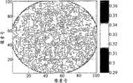
图3示出了在不同的层厚度的情况下针对恒定的总层宽度1040μm和荧光粉浓度10%vol.的平均色度坐标x’(x=50μm),其中Figure 3 shows the average chromaticity coordinate x' (x=50 μm) for a constant total layer width of 1040 μm and a phosphor concentration of 10% vol. in the case of different layer thicknesses, where
(a)100μm,(a) 100 μm,
(b)200μm,(b) 200 μm,
(c)400μm(最优),(c) 400μm (optimum),
(d)600μm,以及(d) 600 μm, and
(e)700μm。(e) 700 μm.
平均色度坐标被示出为图4中所示半球形检测器的像素号的函数。The average chromaticity coordinates are shown as a function of pixel number for the hemispherical detector shown in FIG. 4 .
图5示出了半球形检测器的像素号的平面二维视图。Figure 5 shows a planar two-dimensional view of the pixel numbers of a hemispherical detector.
像素号50与位于LED芯片的有源发光区中心上方右侧的半球形检测器的坐标相对应。像素号0和100分别地与0°和180°的视角相对应。
图3示出了针对总宽度1040μm、横向超出的延伸x=50μm以及荧光粉体积浓度10%,最优层厚度h=400μm给出了最佳(最均匀)角颜色分布结果。Figure 3 shows that for a total width of 1040 μm, a lateral excess extension x=50 μm and a phosphor volume concentration of 10%, an optimal layer thickness h=400 μm gives the best (most uniform) angular color distribution results.
Claims (33)
Translated fromChineseApplications Claiming Priority (3)
| Application Number | Priority Date | Filing Date | Title |
|---|---|---|---|
| EP07107205.2AEP1988583B1 (en) | 2007-04-30 | 2007-04-30 | Light emitting diode module with colour conversion layer designed for a homogenous colour distribution |
| EP07107205.2 | 2007-04-30 | ||
| PCT/EP2008/003159WO2008131877A1 (en) | 2007-04-30 | 2008-04-18 | Led module with colour conversion layer designed for a homogenous colour distribution |
Publications (2)
| Publication Number | Publication Date |
|---|---|
| CN101675536A CN101675536A (en) | 2010-03-17 |
| CN101675536Btrue CN101675536B (en) | 2012-07-18 |
Family
ID=38523381
Family Applications (1)
| Application Number | Title | Priority Date | Filing Date |
|---|---|---|---|
| CN2008800140692AExpired - Fee RelatedCN101675536B (en) | 2007-04-30 | 2008-04-18 | Led module with colour conversion layer designed for a homogenous colour distribution |
Country Status (5)
| Country | Link |
|---|---|
| US (1) | US8309981B2 (en) |
| EP (1) | EP1988583B1 (en) |
| KR (1) | KR101318913B1 (en) |
| CN (1) | CN101675536B (en) |
| WO (1) | WO2008131877A1 (en) |
Families Citing this family (14)
| Publication number | Priority date | Publication date | Assignee | Title |
|---|---|---|---|---|
| US8946987B2 (en)* | 2007-11-07 | 2015-02-03 | Industrial Technology Research Institute | Light emitting device and fabricating method thereof |
| FR2949165B1 (en)* | 2009-08-11 | 2011-10-07 | Oberthur Technologies | MICROCIRCUIT CARD COMPRISING A LIGHT EMITTING DIODE |
| DE102011001928A1 (en)* | 2011-04-08 | 2012-10-11 | Lumitech Produktion Und Entwicklung Gmbh | Color conversion element and lamp |
| US8492182B2 (en)* | 2011-04-29 | 2013-07-23 | Osram Opto Semiconductors Gmbh | Method for the producing of a light-emitting semiconductor chip, method for the production of a conversion die and light-emitting semiconductor chip |
| JP6325536B2 (en)* | 2012-07-05 | 2018-05-16 | コーニンクレッカ フィリップス エヌ ヴェKoninklijke Philips N.V. | Phosphor separated from LED by transparent spacer |
| US8933478B2 (en) | 2013-02-19 | 2015-01-13 | Cooledge Lighting Inc. | Engineered-phosphor LED packages and related methods |
| US8754435B1 (en) | 2013-02-19 | 2014-06-17 | Cooledge Lighting Inc. | Engineered-phosphor LED package and related methods |
| DE102013221644A1 (en) | 2013-04-30 | 2014-10-30 | Tridonic Gmbh & Co Kg | LED module with concave support |
| JP6484982B2 (en)* | 2014-09-30 | 2019-03-20 | 日亜化学工業株式会社 | Method for manufacturing light emitting device |
| CN104752453B (en)* | 2015-03-30 | 2017-09-19 | 深圳市华星光电技术有限公司 | A light emitting device and a liquid crystal display device |
| US20200013932A1 (en)* | 2017-01-24 | 2020-01-09 | Lg Innotek Co., Ltd. | Semiconductor device package |
| KR102362004B1 (en)* | 2017-03-24 | 2022-02-15 | 엘지이노텍 주식회사 | Semiconductor device Package |
| EP4250721A3 (en)* | 2017-02-15 | 2024-02-07 | Lazurite Holdings LLC | Wireless medical imaging system comprising a head unit and a light cable that comprises an integrated light source |
| US11094861B2 (en) | 2018-08-28 | 2021-08-17 | Lg Display Co., Ltd. | Display device |
Citations (2)
| Publication number | Priority date | Publication date | Assignee | Title |
|---|---|---|---|---|
| EP1198016A2 (en)* | 2000-10-13 | 2002-04-17 | LumiLeds Lighting U.S., LLC | Stenciling phosphor layers on light emitting diodes |
| EP1418630A1 (en)* | 2002-11-07 | 2004-05-12 | Matsushita Electric Industrial Co., Ltd. | LED lamp |
Family Cites Families (7)
| Publication number | Priority date | Publication date | Assignee | Title |
|---|---|---|---|---|
| KR100537349B1 (en)* | 1996-06-26 | 2006-02-28 | 오스람 게젤샤프트 미트 베쉬랭크터 하프퉁 | Light-emitting semiconductor component with luminescence conversion element |
| US6635363B1 (en)* | 2000-08-21 | 2003-10-21 | General Electric Company | Phosphor coating with self-adjusting distance from LED chip |
| US6642652B2 (en)* | 2001-06-11 | 2003-11-04 | Lumileds Lighting U.S., Llc | Phosphor-converted light emitting device |
| JP4143732B2 (en)* | 2002-10-16 | 2008-09-03 | スタンレー電気株式会社 | In-vehicle wavelength converter |
| JP2005252222A (en)* | 2004-02-03 | 2005-09-15 | Matsushita Electric Ind Co Ltd | Semiconductor light emitting device, lighting module, lighting device, display element, and method for manufacturing semiconductor light emitting device |
| DE102004047727B4 (en)* | 2004-09-30 | 2018-01-18 | Osram Opto Semiconductors Gmbh | Luminescence diode chip with a converter layer and method for producing a luminescence diode chip with a converter layer |
| DE102004053116A1 (en)* | 2004-11-03 | 2006-05-04 | Tridonic Optoelectronics Gmbh | Light-emitting diode arrangement with color conversion material |
- 2007
- 2007-04-30EPEP07107205.2Apatent/EP1988583B1/ennot_activeNot-in-force
- 2008
- 2008-04-18USUS12/527,179patent/US8309981B2/ennot_activeExpired - Fee Related
- 2008-04-18KRKR1020097022321Apatent/KR101318913B1/ennot_activeExpired - Fee Related
- 2008-04-18WOPCT/EP2008/003159patent/WO2008131877A1/enactiveApplication Filing
- 2008-04-18CNCN2008800140692Apatent/CN101675536B/ennot_activeExpired - Fee Related
Patent Citations (2)
| Publication number | Priority date | Publication date | Assignee | Title |
|---|---|---|---|---|
| EP1198016A2 (en)* | 2000-10-13 | 2002-04-17 | LumiLeds Lighting U.S., LLC | Stenciling phosphor layers on light emitting diodes |
| EP1418630A1 (en)* | 2002-11-07 | 2004-05-12 | Matsushita Electric Industrial Co., Ltd. | LED lamp |
Also Published As
| Publication number | Publication date |
|---|---|
| EP1988583A1 (en) | 2008-11-05 |
| KR20100015900A (en) | 2010-02-12 |
| CN101675536A (en) | 2010-03-17 |
| WO2008131877A8 (en) | 2009-09-24 |
| KR101318913B1 (en) | 2013-10-17 |
| WO2008131877A1 (en) | 2008-11-06 |
| US8309981B2 (en) | 2012-11-13 |
| US20100127293A1 (en) | 2010-05-27 |
| EP1988583B1 (en) | 2016-10-12 |
Similar Documents
| Publication | Publication Date | Title |
|---|---|---|
| CN101675536B (en) | Led module with colour conversion layer designed for a homogenous colour distribution | |
| US9082946B2 (en) | Light emitting module, a lamp, a luminaire and a display device | |
| US9599292B2 (en) | Light emitting module, a lamp, a luminaire and a display device | |
| JP6599295B2 (en) | LIGHT EMITTING ELEMENT HAVING BELT ANGLE REFLECTOR AND MANUFACTURING METHOD | |
| JP5899507B2 (en) | LIGHT EMITTING DEVICE AND LIGHTING DEVICE USING THE SAME | |
| US8558448B2 (en) | Semiconductor light emitting device | |
| JP6735072B2 (en) | LED light source device and projector | |
| US8921877B2 (en) | Semiconductor light-emitting device for producing wavelength-converted light and method for manufacturing the same | |
| JP4238681B2 (en) | Light emitting device | |
| JP5437177B2 (en) | Light emitting device | |
| US9246070B2 (en) | Engineered-phosphor LED packages and related methods | |
| US8803171B2 (en) | Reduced color over angle variation LEDs | |
| CN102057508B (en) | LED module comprising a dome-shaped color conversion layer | |
| CN102484189B (en) | Light emitting device | |
| JP7235944B2 (en) | Light-emitting device and method for manufacturing light-emitting device | |
| JP2012248553A (en) | Light-emitting device and luminaire using the same | |
| US10533729B2 (en) | Light source with LED chip and luminophore layer | |
| JP2013038353A (en) | Light-emitting module | |
| JP2012009696A (en) | Light emitting device and led illuminating equipment | |
| JP6266923B2 (en) | LED light emitting device | |
| JP7285439B2 (en) | planar light source | |
| US12206052B2 (en) | Light-emitting device and planar light source that utilizes multiple wavelength conversion layers | |
| JP2011138843A (en) | Light emitting device | |
| KR20120139077A (en) | Lighting device | |
| JP2018125400A (en) | Light-emitting device and illuminating device |
Legal Events
| Date | Code | Title | Description |
|---|---|---|---|
| C06 | Publication | ||
| PB01 | Publication | ||
| C10 | Entry into substantive examination | ||
| SE01 | Entry into force of request for substantive examination | ||
| C14 | Grant of patent or utility model | ||
| GR01 | Patent grant | ||
| CF01 | Termination of patent right due to non-payment of annual fee | Granted publication date:20120718 Termination date:20210418 | |
| CF01 | Termination of patent right due to non-payment of annual fee |