CN101673013A - Liquid crystal display device including touch panel - Google Patents
Liquid crystal display device including touch panelDownload PDFInfo
- Publication number
- CN101673013A CN101673013ACN200810182593ACN200810182593ACN101673013ACN 101673013 ACN101673013 ACN 101673013ACN 200810182593 ACN200810182593 ACN 200810182593ACN 200810182593 ACN200810182593 ACN 200810182593ACN 101673013 ACN101673013 ACN 101673013A
- Authority
- CN
- China
- Prior art keywords
- electrode
- liquid crystal
- electrodes
- substrate
- touch panel
- Prior art date
- Legal status (The legal status is an assumption and is not a legal conclusion. Google has not performed a legal analysis and makes no representation as to the accuracy of the status listed.)
- Granted
Links
Images


Classifications
- G—PHYSICS
- G06—COMPUTING OR CALCULATING; COUNTING
- G06F—ELECTRIC DIGITAL DATA PROCESSING
- G06F3/00—Input arrangements for transferring data to be processed into a form capable of being handled by the computer; Output arrangements for transferring data from processing unit to output unit, e.g. interface arrangements
- G06F3/01—Input arrangements or combined input and output arrangements for interaction between user and computer
- G06F3/03—Arrangements for converting the position or the displacement of a member into a coded form
- G06F3/041—Digitisers, e.g. for touch screens or touch pads, characterised by the transducing means
- G06F3/0412—Digitisers structurally integrated in a display
- G—PHYSICS
- G02—OPTICS
- G02F—OPTICAL DEVICES OR ARRANGEMENTS FOR THE CONTROL OF LIGHT BY MODIFICATION OF THE OPTICAL PROPERTIES OF THE MEDIA OF THE ELEMENTS INVOLVED THEREIN; NON-LINEAR OPTICS; FREQUENCY-CHANGING OF LIGHT; OPTICAL LOGIC ELEMENTS; OPTICAL ANALOGUE/DIGITAL CONVERTERS
- G02F1/00—Devices or arrangements for the control of the intensity, colour, phase, polarisation or direction of light arriving from an independent light source, e.g. switching, gating or modulating; Non-linear optics
- G02F1/01—Devices or arrangements for the control of the intensity, colour, phase, polarisation or direction of light arriving from an independent light source, e.g. switching, gating or modulating; Non-linear optics for the control of the intensity, phase, polarisation or colour
- G02F1/13—Devices or arrangements for the control of the intensity, colour, phase, polarisation or direction of light arriving from an independent light source, e.g. switching, gating or modulating; Non-linear optics for the control of the intensity, phase, polarisation or colour based on liquid crystals, e.g. single liquid crystal display cells
- G02F1/133—Constructional arrangements; Operation of liquid crystal cells; Circuit arrangements
- G02F1/1333—Constructional arrangements; Manufacturing methods
- G02F1/13338—Input devices, e.g. touch panels
- G—PHYSICS
- G06—COMPUTING OR CALCULATING; COUNTING
- G06F—ELECTRIC DIGITAL DATA PROCESSING
- G06F3/00—Input arrangements for transferring data to be processed into a form capable of being handled by the computer; Output arrangements for transferring data from processing unit to output unit, e.g. interface arrangements
- G06F3/01—Input arrangements or combined input and output arrangements for interaction between user and computer
- G06F3/03—Arrangements for converting the position or the displacement of a member into a coded form
- G06F3/041—Digitisers, e.g. for touch screens or touch pads, characterised by the transducing means
- G06F3/0416—Control or interface arrangements specially adapted for digitisers
- G06F3/04164—Connections between sensors and controllers, e.g. routing lines between electrodes and connection pads
- G—PHYSICS
- G06—COMPUTING OR CALCULATING; COUNTING
- G06F—ELECTRIC DIGITAL DATA PROCESSING
- G06F3/00—Input arrangements for transferring data to be processed into a form capable of being handled by the computer; Output arrangements for transferring data from processing unit to output unit, e.g. interface arrangements
- G06F3/01—Input arrangements or combined input and output arrangements for interaction between user and computer
- G06F3/03—Arrangements for converting the position or the displacement of a member into a coded form
- G06F3/041—Digitisers, e.g. for touch screens or touch pads, characterised by the transducing means
- G06F3/044—Digitisers, e.g. for touch screens or touch pads, characterised by the transducing means by capacitive means
- G06F3/0445—Digitisers, e.g. for touch screens or touch pads, characterised by the transducing means by capacitive means using two or more layers of sensing electrodes, e.g. using two layers of electrodes separated by a dielectric layer
- G—PHYSICS
- G06—COMPUTING OR CALCULATING; COUNTING
- G06F—ELECTRIC DIGITAL DATA PROCESSING
- G06F3/00—Input arrangements for transferring data to be processed into a form capable of being handled by the computer; Output arrangements for transferring data from processing unit to output unit, e.g. interface arrangements
- G06F3/01—Input arrangements or combined input and output arrangements for interaction between user and computer
- G06F3/03—Arrangements for converting the position or the displacement of a member into a coded form
- G06F3/041—Digitisers, e.g. for touch screens or touch pads, characterised by the transducing means
- G06F3/044—Digitisers, e.g. for touch screens or touch pads, characterised by the transducing means by capacitive means
- G06F3/0446—Digitisers, e.g. for touch screens or touch pads, characterised by the transducing means by capacitive means using a grid-like structure of electrodes in at least two directions, e.g. using row and column electrodes
- G—PHYSICS
- G06—COMPUTING OR CALCULATING; COUNTING
- G06F—ELECTRIC DIGITAL DATA PROCESSING
- G06F2203/00—Indexing scheme relating to G06F3/00 - G06F3/048
- G06F2203/041—Indexing scheme relating to G06F3/041 - G06F3/045
- G06F2203/04111—Cross over in capacitive digitiser, i.e. details of structures for connecting electrodes of the sensing pattern where the connections cross each other, e.g. bridge structures comprising an insulating layer, or vias through substrate
- G—PHYSICS
- G06—COMPUTING OR CALCULATING; COUNTING
- G06F—ELECTRIC DIGITAL DATA PROCESSING
- G06F3/00—Input arrangements for transferring data to be processed into a form capable of being handled by the computer; Output arrangements for transferring data from processing unit to output unit, e.g. interface arrangements
- G06F3/01—Input arrangements or combined input and output arrangements for interaction between user and computer
- G06F3/03—Arrangements for converting the position or the displacement of a member into a coded form
- G06F3/041—Digitisers, e.g. for touch screens or touch pads, characterised by the transducing means
- G06F3/044—Digitisers, e.g. for touch screens or touch pads, characterised by the transducing means by capacitive means
- G06F3/0448—Details of the electrode shape, e.g. for enhancing the detection of touches, for generating specific electric field shapes, for enhancing display quality
Landscapes
- Engineering & Computer Science (AREA)
- Physics & Mathematics (AREA)
- Theoretical Computer Science (AREA)
- General Engineering & Computer Science (AREA)
- General Physics & Mathematics (AREA)
- Human Computer Interaction (AREA)
- Nonlinear Science (AREA)
- Mathematical Physics (AREA)
- Chemical & Material Sciences (AREA)
- Crystallography & Structural Chemistry (AREA)
- Optics & Photonics (AREA)
- Liquid Crystal (AREA)
- Computer Networks & Wireless Communication (AREA)
- Position Input By Displaying (AREA)
Abstract
Translated fromChineseDescription
Translated fromChinese本申请要求2008年9月12日申请的韩国专利申请No.P08-090236的优先权,将该申请在此以全文引用的方式结合以作用于各种目的的参考。This application claims priority from Korean Patent Application No. P08-090236 filed on September 12, 2008, which is hereby incorporated by reference in its entirety for all purposes.
技术领域technical field
本发明涉及一种液晶显示器件,更具体地说,涉及一种其中触摸面板嵌入在液晶面板中的液晶显示器件,由此有助于减少工序数量且容易组装。The present invention relates to a liquid crystal display device, and more particularly, to a liquid crystal display device in which a touch panel is embedded in a liquid crystal panel, thereby contributing to a reduction in the number of processes and easy assembly.
背景技术Background technique
随着现代社会对信息依赖的不断提高,可视地显示电子信息信号的显示领域正在快速地发展。因而,现已发展了具有出色性能,如厚度薄,重量轻且能耗低的各种平板显示器件,它们已迅速取代了普通的阴极射线管(CRT)。With the continuous improvement of modern society's dependence on information, the field of display for visually displaying electronic information signals is developing rapidly. Accordingly, various flat panel display devices having excellent properties such as thin thickness, light weight and low power consumption have been developed, and they have rapidly replaced general cathode ray tubes (CRTs).
平板显示器件的实例例如包括液晶显示(LCD)器件、等离子体面板显示(PDP)器件、场发射显示(FED)器件和电致发光显示(ELD)器件等。作为一基本元件,这些器件通常都包括形成图像的平板显示面板。平板显示面板如此构造,即彼此面对地粘合一对透明绝缘基板,在该对透明绝缘基板之间插入固有的照明或偏振材料层。Examples of flat panel display devices include, for example, liquid crystal display (LCD) devices, plasma panel display (PDP) devices, field emission display (FED) devices, electroluminescence display (ELD) devices, and the like. These devices generally include, as a basic element, a flat display panel forming an image. The flat panel display panel is constructed by bonding a pair of transparent insulating substrates facing each other with an intrinsic lighting or polarizing material layer interposed between the pair of transparent insulating substrates.
在上述显示器件中,LCD器件设计成通过使用电场调节液晶的光透射率来显示图像。为此,LCD器件包括具有液晶单元的显示面板、将光照射到显示面板的背光单元和驱动液晶面板的驱动电路。Among the above display devices, the LCD device is designed to display images by adjusting light transmittance of liquid crystals using an electric field. To this end, an LCD device includes a display panel having a liquid crystal cell, a backlight unit that irradiates light to the display panel, and a driving circuit that drives the liquid crystal panel.
显示面板设置有彼此交叉以限定多个单元像素区域的多条栅线和多条数据线。在该情形中,每个像素区域都由彼此相对的薄膜晶体管阵列基板和滤色器阵列基板、位于两个基板之间用于保持液晶盒间隙的衬垫料、和填充在液晶盒间隙中的液晶所组成。The display panel is provided with a plurality of gate lines and a plurality of data lines crossing each other to define a plurality of unit pixel regions. In this case, each pixel region is composed of a thin film transistor array substrate and a color filter array substrate facing each other, a spacer between the two substrates for maintaining the liquid crystal cell gap, and a liquid crystal cell filled in the liquid crystal cell gap. composed of liquid crystals.
薄膜晶体管阵列基板包括栅线和数据线、形成在栅线和数据线的交点处用作开关器件的薄膜晶体管、布置在每一液晶单元中并与薄膜晶体管连接的像素电极、和涂敷在所有上述元件之上的定向膜。来自驱动电路的信号通过各个焊盘供给到栅线和数据线。The thin film transistor array substrate includes gate lines and data lines, thin film transistors used as switching devices formed at intersections of the gate lines and data lines, pixel electrodes arranged in each liquid crystal cell and connected to the thin film transistors, and coated on all Orientation film on top of the above elements. Signals from the driving circuit are supplied to the gate lines and the data lines through the respective pads.
薄膜晶体管响应于供给到数据线的信号以及响应于供给到栅线的扫描信号,给像素电极供给像素电压。The thin film transistor supplies a pixel voltage to the pixel electrode in response to a signal supplied to the data line and in response to a scan signal supplied to the gate line.
滤色器阵列基板包括布置在每一像素单元的滤色器、用于分割滤色器并折射外部光的黑矩阵、给液晶单元公共地供给基准电压的公共电极、和涂敷在所有上述元件之上的定向膜。The color filter array substrate includes a color filter arranged in each pixel unit, a black matrix for dividing the color filter and refracting external light, a common electrode for commonly supplying a reference voltage to the liquid crystal unit, and coatings on all the above elements oriented film on top.
在将独立制造的薄膜晶体管基板和滤色器阵列基板对准之后,将所制得的薄膜晶体管基板和滤色器阵列基板彼此面对地粘合,注入液晶并密封,由此完成了显示面板的制造。After aligning the independently manufactured thin film transistor substrate and color filter array substrate, the manufactured thin film transistor substrate and color filter array substrate are bonded facing each other, liquid crystal is injected and sealed, thereby completing the display panel manufacturing.
为如上所述制造的LCD器件添加触摸面板的需求现在正日益增加。触摸面板设计成用于传感人手或其他输入部件的触摸位置并响应于传感的触摸位置来传输信息。当前,已经将这种触摸面板粘附到了LCD器件的外表面。The need to add a touch panel to the LCD device manufactured as described above is now increasing. The touch panel is designed to sense the touch location of a human hand or other input member and transmit information in response to the sensed touch location. Currently, such touch panels have been adhered to the outer surfaces of LCD devices.
下面,将参照附图描述现有普通的粘附有触摸面板的LCD器件。Hereinafter, a conventional conventional touch panel-attached LCD device will be described with reference to the accompanying drawings.
图1是图解现有普通的粘附有触摸面板的LCD器件的示意图。FIG. 1 is a schematic view illustrating a conventional touch panel-attached LCD device.
如图1中所示,现有普通的粘附有触摸面板的LCD器件包括由第一和第二基板1和2、填充在基板1和2之间的液晶层3以及分别粘附到第一和第二基板1和2后表面的第一和第二偏振器4a和4b组成的液晶面板10;和设置在液晶面板10上并以电容方式驱动的触摸面板20;和用于保护触摸面板20顶部的盖玻片(cover glass)30。As shown in FIG. 1, the existing common LCD device with a touch panel is composed of first and
在液晶面板10的第一基板1上设置有薄膜晶体管(TFT)阵列,其由彼此交叉以限定像素区域的栅线和数据线、形成在栅线和数据线的交点处的TFT、和各个像素区域(没有示出)中的像素电极组成。On the first substrate 1 of the
在第二基板2上设置有滤色器阵列,其由黑矩阵层、滤色器层和公共电极组成。A color filter array is arranged on the
触摸面板20的内部构造根据触摸面板的驱动方式而变化。例如,在电容式触摸面板的情形中,将触摸面板设计成通过触摸点处的电容变化来传感触摸位置,设置彼此交叉的第一和第二电极,从而能通过电极之间的电容值变化来进行传感。The internal structure of the touch panel 20 changes according to the driving method of the touch panel. For example, in the case of a capacitive touch panel, the touch panel is designed to sense the touch position through the capacitance change at the touch point, and the first and second electrodes intersecting each other are arranged so that the capacitance value between the electrodes can be changed. for sensing.
为了保护触摸面板20,在触摸面板20的顶部设置盖玻片30。In order to protect the touch panel 20 , a
由于触摸面板20作为液晶面板10的外壳而形成,所以上述普通的粘附有触摸面板的LCD器件在触摸面板20与液晶面板10之间需要粘结层(没有示出)。在该情形中,必须单独制造液晶面板10和触摸面板20,且需要将触摸面板20和液晶面板10彼此粘附的工序。Since the touch panel 20 is formed as a case of the
下面述上述普通的粘附有触摸面板的LCD器件的问题。The problems of the above-mentioned conventional touch panel-attached LCD device will be described below.
触摸面板作为液晶面板的外壳而形成,因此,必须在触摸面板与液晶面板之间设置粘结层。这将不可避免地需要额外的粘附工序。此外,如果触摸面板和液晶面板对不准,则很难分离粘附到液晶面板的触摸面板,强制的方式将其分离则会损坏触摸面板。Since the touch panel is formed as a casing of the liquid crystal panel, it is necessary to provide an adhesive layer between the touch panel and the liquid crystal panel. This will inevitably require an additional adhesion process. In addition, if the touch panel and the liquid crystal panel are misaligned, it is difficult to separate the touch panel adhered to the liquid crystal panel, and separating it in a forcible manner may damage the touch panel.
此外,由于工序数增加,在触摸面板与液晶面板之间粘附粘结层存在增加工序时间和成本的危险。In addition, adhering an adhesive layer between the touch panel and the liquid crystal panel risks increasing process time and cost due to an increase in the number of processes.
就触摸面板粘附到液晶面板的构造而言,整个LCD器件具有至少触摸面板、液晶面板、包围液晶面板的模块和盖玻片的总厚度。假定在诸如便携式电话这样的小型器件中使用这种粘附有触摸面板的LCD器件,则整个LCD器件较厚的厚度会成为负担。In terms of the configuration in which the touch panel is adhered to the liquid crystal panel, the entire LCD device has a total thickness of at least the touch panel, the liquid crystal panel, the module surrounding the liquid crystal panel, and the cover glass. Assuming that such a touch panel-attached LCD device is used in a small-sized device such as a cellular phone, the thick thickness of the entire LCD device becomes a burden.
发明内容Contents of the invention
因此,本发明涉及一种内嵌触摸面板的液晶显示器件,其基本克服了由于现有技术的限制和缺点导致的一个或多个问题。Accordingly, the present invention is directed to a touch panel embedded liquid crystal display device that substantially overcomes one or more of the problems due to limitations and disadvantages of the related art.
本发明的优点是提供了一种触摸面板嵌入在液晶面板中的内嵌触摸面板的液晶显示器件,其减小了工序数且易于组装。The advantage of the present invention is to provide a touch panel embedded liquid crystal display device in which the touch panel is embedded in the liquid crystal panel, which reduces the number of processes and is easy to assemble.
将在下面的描述中列出本发明其他的特征和优点,且其中一部分从所述描述中变得显而易见,或者通过对本发明的实践可以理解到。通过在说明书和权利要求书以及附图中特别指出的结构可实现和获得本发明的目的和其它的优点。Additional features and advantages of the invention will be set forth in the description which follows, and in part will be apparent from the description, or may be learned by practice of the invention. The objectives and other advantages of the invention will be realized and attained by the structure particularly pointed out in the written description and claims hereof as well as the appended drawings.
为了实现这些和其它的优点并根据本发明的目的,如这里广义和具体的描述,本发明的液晶显示器件包括彼此相对的第一和第二基板;形成在所述第一基板上的薄膜晶体管阵列;形成在所述第二基板上的触摸传感部,其包括彼此垂直交叉的多个透明X电极和多个Y电极以及在所述X电极与所述Y电极之间的第一透明绝缘膜;形成在所述触摸传感部上的滤色器阵列;和形成在所述薄膜晶体管阵列与所述滤色器阵列之间的液晶层。To achieve these and other advantages and in accordance with the purpose of the present invention, as broadly and specifically described herein, a liquid crystal display device of the present invention includes first and second substrates facing each other; a thin film transistor formed on said first substrate array; a touch-sensing portion formed on the second substrate, which includes a plurality of transparent X electrodes and a plurality of Y electrodes perpendicularly intersecting each other and a first transparent insulating layer between the X electrodes and the Y electrodes a film; a color filter array formed on the touch sensing portion; and a liquid crystal layer formed between the thin film transistor array and the color filter array.
应当理解,前面的一般性描述和下面的详细描述都是典型性的和解释性的,意在提供对如权利要求书中所述的本发明进一步的解释。It is to be understood that both the foregoing general description and the following detailed description are exemplary and explanatory and are intended to provide further explanation of the invention as claimed.
附图说明Description of drawings
给本发明提供进一步理解并构成说明书一部分的附图图解了本发明的实施方式并与说明书一起用于解释本发明的原理。The accompanying drawings, which are included to provide a further understanding of the invention and constitute a part of this specification, illustrate embodiments of the invention and together with the description serve to explain the principle of the invention.
在附图中:In the attached picture:
图1是图解现有普通的粘附有触摸面板的液晶显示器件的示意图;FIG. 1 is a schematic diagram illustrating a conventional conventional liquid crystal display device with a touch panel attached;
图2是图解根据本发明的内嵌触摸面板的液晶显示器件的截面图;2 is a cross-sectional view illustrating a touch panel-embedded liquid crystal display device according to the present invention;
图3A到3F是图解用于制造根据本发明的内嵌触摸面板的液晶显示器件的方法的截面图;3A to 3F are cross-sectional views illustrating a method for manufacturing a touch panel-embedded liquid crystal display device according to the present invention;
图4A和4B是图解当在旋转90度的方向上看时,在图3C之后的工序的截面图;4A and 4B are cross-sectional views illustrating a process after FIG. 3C when viewed in a direction rotated 90 degrees;
图5是图解在根据本发明的内嵌触摸面板的液晶显示器件中设置的上基板的平面图;5 is a plan view illustrating an upper substrate provided in a touch panel-embedded liquid crystal display device according to the present invention;
图6A和6B是图解在根据本发明的液晶显示器件中的X和Y电极的改进形式的平面图;6A and 6B are plan views illustrating modified forms of X and Y electrodes in a liquid crystal display device according to the present invention;
图7是图解信号供给器与彼此粘结的上下基板之间的连接关系的平面图;和7 is a plan view illustrating a connection relationship between a signal supplier and upper and lower substrates bonded to each other; and
图8是图解X和Y电极之间的电容变化相对于两个电极之间的绝缘膜的厚度的曲线。FIG. 8 is a graph illustrating a change in capacitance between X and Y electrodes with respect to the thickness of an insulating film between the two electrodes.
具体实施方式Detailed ways
现在将参照本发明的实施方式对本发明进行详细的描述,附图中图解了其实例。The invention will now be described in detail with reference to embodiments of the invention, examples of which are illustrated in the accompanying drawings.
下面将参照附图详细描述根据本发明的内嵌触摸面板的液晶显示器件及其制造方法。A touch panel-embedded liquid crystal display device and a manufacturing method thereof according to the present invention will be described in detail below with reference to the accompanying drawings.
图2是图解根据本发明的内嵌触摸面板的液晶显示器件的截面图;2 is a cross-sectional view illustrating a touch panel-embedded liquid crystal display device according to the present invention;
如图2中所示,本发明的内嵌触摸面板的液晶显示器件包括彼此相对的薄膜晶体管阵列基板1100和滤色器阵列基板1200、填充在薄膜晶体管阵列基板1100和滤色器阵列基板1200之间的液晶层130、分别设置在薄膜晶体管阵列基板1100和滤色器阵列基板1200后表面上的第一和第二偏振器150a和150b。As shown in FIG. 2 , the liquid crystal display device with an embedded touch panel of the present invention includes a thin film
薄膜晶体管阵列基板1100包括第一基板110和形成在第一基板110上的薄膜晶体管阵列115。薄膜晶体管阵列115由彼此交叉以限定像素区域的栅线(没有示出)和数据线(没有示出)、形成在各个像素区域中的像素电极(没有示出)、以及形成在栅线和数据线的交叉点处的薄膜晶体管(没有示出)组成。The thin film
滤色器阵列基板1200包括第二基板120和依次形成在第二基板120上的触摸传感部140和滤色器阵列125。滤色器阵列125由黑矩阵层1251、滤色器层1252;1252a,1252b和1252c、保护层1253、和形成在保护层1253整个表面上的公共电极1254(见图3F)所组成。The color
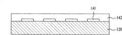
触摸传感部140由形成在第二基板120上且在X轴方向上彼此隔开一预定距离的多个X电极141(见图3B)、形成在包括X电极141的第二基板120整个表面上的第一绝缘膜142、形成在第一绝缘膜142上且在与X电极141交叉的方向上彼此隔开一预定距离的Y电极143(见图4B)、以及形成在Y电极143整个表面上的第二绝缘膜144所组成。The
触摸传感部140的X电极141和Y电极143都是透明电极。第一绝缘膜142由透明有机绝缘膜形成,从而使X电极141上的平面实现平坦化。Both the
第一绝缘膜142例如具有0.1~5μm的厚度,且由有机绝缘膜形成,第一绝缘膜142像感光亚克力一样是透明的并具有较低的介电常数。第一绝缘膜142用于使形成X电极141之后的平面实现平坦化,还可用于防止在X电极141和Y电极143交叉点处的负载增加。The first
X电极141是在X轴方向延伸的棒形电极(见图5)。Y电极143是在与X电极141交叉的Y轴方向上延伸的棒形电极(见图5)。X电极141和Y电极143的棒形是示例性的。X电极141和Y电极143可包括除棒形之外的其他形状,并可以在除交叉点之外的位置规则地形成。The
X电极141和Y电极143中的至少其中之一在两电极的交叉点处的宽度比其在其余区域的宽度要小(见图6A)。该构造减小了X电极141和Y电极143之间的负载,这对于以高灵敏度传感X电极141和Y电极143之间的电容是有利的。At least one of the
X电极141和Y电极143由氧化铟锡(ITO)、氧化铟锌(IZO)和氧化钢锡锌(ITZO)中的任意一个物质形成。The
根据具体场合的需求,可省略触摸传感部140与滤色器阵列125之间的第二绝缘膜144。然而,设置第二绝缘膜144可以使Y电极143之上的平面实现平坦化,并使触摸传感部140与形成在滤色器阵列125顶部的公共电极1254绝缘,由此防止X电极141和Y电极143的触摸传感操作对薄膜晶体管阵列115与公共电极1254之间产生的垂直电场造成影响。According to the requirements of specific occasions, the second
第一基板110和第二基板120包括第一区域和第二区域,所述的第一区域和第二区域分别限定在所述两基板彼此不重叠的侧部区域中部分中。图像信号供给器310与第一区域连接,用于给薄膜晶体管阵列115施加信号。触摸面板信号控制器320与第二区域连接,用于执行相对于X和Y电极141和143的电压施加和信号检测。The
X电极141和Y电极143中的任意一个电极用作施加有电压的驱动电极,另一个用作检测电压信号的传感电极(sensing electrode)。X电极141和Y电极143中的每一个电极都与位于所述电极一端的焊盘(180,见图5)相连接。Any one of the
触摸传感部140连续给所述多个驱动电极施加电压信号并检测在所述传感电极处的电压值,由此测量在发生触摸时在X电极141和Y电极143之间的电容变化。这样,可检测到触摸的存在和触摸的位置。The
可在第二基板120的第二偏振器150b上进一步设置盖玻片(300,见图3F),但根据需要,当第二基板120具有抵抗外部压力的坚固性时,则所述的盖玻片可以省略。A cover glass (300, see FIG. 3F ) may be further provided on the
在上述本发明的内嵌触摸面板的液晶显示器件中,触摸传感操作按如下方式来实现。In the touch panel-embedded liquid crystal display device of the present invention described above, the touch sensing operation is realized as follows.
如果连续给X电极141施加电压,则X电极141与Y电极143之间的电容会根据是否发生触摸而变化。通过读取电容的这种变化和从Y电极143输出的电流的变化就可以传感触摸位置。If a voltage is continuously applied to the
在该情形中,在单个帧中完成给X电极141连续施加电压和在Y电极143处的电流检测。因此,当在几个位置处同时发生触摸时,可以传感多个触摸。In this case, continuous voltage application to the
下面将参照附图描述用于制造本发明的内嵌触摸面板的液晶显示器件的方法。A method for manufacturing the touch panel-embedded liquid crystal display device of the present invention will be described below with reference to the accompanying drawings.
图3A到3F图解了用于制造根据本发明的内嵌触摸面板的液晶显示器件的方法。图4A和4B图解了当在旋转90度的方向上看时,在图3C之后的工序。3A to 3F illustrate a method for manufacturing a touch panel-embedded liquid crystal display device according to the present invention. 4A and 4B illustrate the process following FIG. 3C when viewed in a direction rotated 90 degrees.
如图3A中所示,在第二基板120的整个表面上沉积第一透明电极层141a。As shown in FIG. 3A , a first
在透明电极层141a上涂覆第一光致抗蚀剂膜160之后,在第一光致抗蚀剂膜160上排列第一掩模200,在所述的第一掩模200中在与将要形成的X电极对应的位置处限定有遮光部分210。使用第一掩模200将第一光致抗蚀剂膜160曝光。曝光工序使第一光致抗蚀剂膜160改性。就是说,第一光致抗蚀剂膜160的被辐射光的部分变为改性的部分160a,该改性的部分160a在随后的显影工序过程中被移除。在该情形中,第一掩模200如此构造,即在例如由石英形成的透明基板205上形成有与遮光部分210对应的图案。After the
这里,第一光致抗蚀剂膜160是正型的,其中通过曝光和显影工序移除受光部分,第一掩模200具有相应的类型。可用负型的替代上述第一光致抗蚀剂膜160,因此,第一掩模200可以具有相反的类型,其中遮光部分210和上述第一掩模200的开口是反向的。Here, the
在完成了曝光工序之后,从第二基板120移除第一掩模200。After the exposure process is completed, the
接着,使用显影工序之后残留的第一光致抗蚀剂膜160选择性地移除第一透明电极层141a,以形成X电极141。Next, the first
然后,通过剥离方法移除残留的第一光致抗蚀剂膜160。Then, the remaining
如图3B中所示,在包括X电极141的第二基板120的整个表面上形成第一绝缘膜142。As shown in FIG. 3B , a first
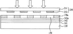
如图3C和4A中所示,在第一绝缘膜142的整个表面上形成第二透明电极层143a,然后依次在第二透明电极层143a的整个表面上形成第二光致抗蚀剂膜170。在第二光致抗蚀剂膜170上排列第二掩模250,在所述的第二掩模250中,在与将要形成的Y电极对应的位置处限定有遮光部分252。在该情形中,第二掩模250如此构造,即在例如由石英形成的透明基板251上形成有与遮光部分252对应的图案。As shown in FIGS. 3C and 4A, a second
图3C是沿与X电极141交叉的Y轴方向的截面图,图4A是沿X电极141的纵向方向,即与图4A正交的X轴方向的截面图。3C is a cross-sectional view along the Y-axis direction intersecting the X-electrode 141 , and FIG. 4A is a cross-sectional view along the longitudinal direction of the
类似地,第二光致抗蚀剂膜170是正型的,其中通过曝光和显影工序移除受光部分,第二掩模250具有相应的类型。第二掩模250的遮光部分252限定在与第一掩模200的遮光部分正交的方向上。因此,如图4A中所示,当在X轴方向上看时,可看到曝光和显影的部分。Similarly, the
可用负型的替代第二光致抗蚀剂膜170,因此,第二掩模250可以具有反向的类型,其中遮光部分252和上述第二掩模250的开口是反向的。The
在完成了曝光工序之后,从第二基板120移除第二掩模250。After the exposure process is completed, the
接着,使用显影工序之后残留的第二光致抗蚀剂膜170选择性地移除第二透明电极层143a,以形成Y电极143。Next, the second
然后,通过剥离方法移除残留的第二光致抗蚀剂膜170。Then, the remaining
如图4B中所示,在包括Y电极143的第一绝缘膜142的整个表面上形成具有平坦表面的第二绝缘膜144。由于Y电极143具有相对薄的厚度,所以很容易使形成在Y电极143上的第二绝缘膜144平坦化。因此,第二绝缘膜144比第一绝缘膜142薄,或者可以省略掉。这里,当省略第二绝缘膜144时,可在形成有Y电极143的第一绝缘膜142上直接形成下面将要描述的滤色器阵列125。As shown in FIG. 4B , a second
X电极141、Y电极143和所述该两个电极之间的第一绝缘膜142限定了触摸传感部140。The
如图3D中所示,在第二绝缘膜144上形成与各个像素区域的边界对应的黑矩阵层1251。As shown in FIG. 3D , a
接着,形成对应于各个像素区域且与黑矩阵层1251部分重叠的红色、绿色和蓝色(RGB)滤色器层1252;1252a,1252b和1252c。Next, red, green and blue (RGB)
接着,在包括黑矩阵层1251和RGB滤色器层1252的第二绝缘膜144的整个表面上形成保护层1253,从而使整个平面平坦化。Next, a
接着,在外覆层1253上形成公共电极1254。Next, a
这里,黑矩阵层1251、滤色器层1252、保护层1253和公共电极1254限定了滤色器阵列125。Here, the
如上所述,在第二基板120上形成了触摸传感部140和滤色器阵列125,由此制备了滤色器阵列基板1200。As described above, the
为了与滤色器阵列基板1200相对应,制备了薄膜晶体管阵列基板1100。In order to correspond to the color
薄膜晶体管阵列基板1100包括第一基板110和形成在第一基板110上的薄膜晶体管阵列115。The thin film
尽管没有详细图解,但薄膜晶体管阵列115由在对应于黑矩阵层1251的彼此交叉以限定像素区域的栅线(没有示出)和数据线(没有示出)、形成在各个像素区域中的像素电极(没有示出)、和形成在栅线和数据线交叉点处的薄膜晶体管(没有示出)所组成。Although not illustrated in detail, the thin
之后,在薄膜晶体管阵列基板1100或滤色器阵列基板1200上加载液晶。Afterwards, liquid crystals are loaded on the thin film
如图3E中所示,在将其上没有加载液晶的基板1100或1200翻转之后,彼此相对地设置薄膜晶体管阵列基板1100和滤色器阵列基板1200。As shown in FIG. 3E, after the
当加载的液晶分布在薄膜晶体管阵列基板1100和滤色器阵列基板1200之间的空间中时,就形成了液晶层130。When the loaded liquid crystal is distributed in the space between the thin film
如图3F中所示,分别在薄膜晶体管阵列基板1100和滤色器阵列基板1200的后表面处形成第一和第二偏振器150a和150b。As shown in FIG. 3F, first and
接着,将盖玻片300粘附到第二偏振器150b的顶部。所述的盖玻片300用于防止当外部压力施加到液晶面板时对液晶面板的破坏或其他损害。如果第二基板120具有足以抵抗外部压力的坚固性,则可省略盖玻片300。Next, a
图5是图解在根据本发明的内嵌触摸面板的液晶显示器件中设置的上基板的平面图。5 is a plan view illustrating an upper substrate provided in a touch panel-embedded liquid crystal display device according to the present invention.
如图5中所示,为了基于有规则的排列来进行传感,将多个X电极141和Y电极143彼此交叉的方式来布置,且每个X电极141和Y电极143彼此都隔开一相等的距离。As shown in FIG. 5 , in order to perform sensing based on a regular arrangement, a plurality of
第二基板120设置有对应于各个X电极141的电压供给焊盘180和对应于各个Y电极143的电压检测焊盘。X电极141和Y电极143通过连接线185与焊盘180连接。The
连接线185和各个焊盘180与X电极141和Y电极143一起形成在第二基板120的内表面。参照图3F,焊盘180形成在第二基板120的与第一基板110面对的表面处并与柔性印刷电路版(FPC)触摸面板信号控制器(320,见图7)连接,该柔性印刷电路版触摸面板信号控制器与施加电信号的系统控制器连接。The connection lines 185 and the
图6A和6B是图解X和Y电极的改进实施方式的平面图。6A and 6B are plan views illustrating modified embodiments of X and Y electrodes.
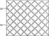
图6A图解了如上所述的图5的X电极141和Y电极143的放大的交点。为了减小X电极141和Y电极143的交点的面积,在X电极141与Y电极143重叠的区域处减小X电极141的宽度。FIG. 6A illustrates an enlarged intersection of the
在本发明的内嵌触摸面板的液晶显示器件的情形中,检测在触摸点处X电极141与Y电极143之间的电容变化,从而传感触摸位置。在该情形中,当X电极141和Y电极143的交点具有较大的面积时,交点处会承受增大的负载,由此使得难以检测到电容的变化。为了解决该问题,在X电极141和Y电极143的交点处减小X电极141的宽度。尽管图解了减小X电极141的宽度,但作为另一个实施方式,也可减小Y电极143的宽度。In the case of the touch panel-embedded liquid crystal display device of the present invention, a capacitance change between the
在图6B中所示的改进形式中,X电极241和Y电极243具有相同的面积并在所述两电极的交点处宽度分别减小,以使在检测电容时产生的负载最小化。尽管图解了X和Y电极241和243具有菱形,但如果X电极和Y电极在第二基板120上占据相同的面积,则其他改进形状也是可以的。In a modified form shown in FIG. 6B, the
图7是图解信号供给器与彼此粘结的上下基板之间的连接关系的平面图。7 is a plan view illustrating a connection relationship between a signal supplier and upper and lower substrates bonded to each other.
如图7中所示,在本发明的内嵌触摸面板的液晶显示器件中,第一基板110和第二基板120彼此以这样的方式粘结,即所述的两基板从它们的相对侧分别突出,而不是完全彼此重叠。这里,从第一基板110突出的区域称作第一区域,从第二基板120突出的区域称作第二区域。As shown in FIG. 7, in the liquid crystal display device with built-in touch panel of the present invention, the
图像信号供给器310与从第一基板110突出的第一区域的边缘连接,从而给薄膜晶体管阵列151施加信号。触摸面板信号控制器320与从第二基板120突出的第二区域的边缘连接,从而将信号施加到触摸传感部。在该情形中,触摸面板信号控制器320与上述的电压供给焊盘和电压检测焊盘180连接。图像信号供给器310与形成在第一基板110上的栅线焊盘部分和数据线焊盘部分连接。The
参照图7,图像信号供给器310和触摸面板信号控制器320由FPC(柔性印刷电路版)形成并可折叠地置于第一基板110的下侧。第二区域包含给X电极141施加电压信号的电压供给焊盘180和检测从Y电极143输出的信号的电压检测焊盘180,这些焊盘都通过连接线185与触摸传感部140的X电极141和Y电极143连接。电压供给焊盘180和电压检测焊盘180与触摸面板信号控制器320连接。Referring to FIG. 7 , an
图像信号供给器310和触摸面板信号控制器320由软性的FPC形成并在安装时可折叠地置于液晶模块的下侧。The
图8是图解X和Y电极之间的电容变化相对于两个电极之间的绝缘膜的厚度的曲线。FIG. 8 is a graph illustrating a change in capacitance between X and Y electrodes with respect to the thickness of an insulating film between the two electrodes.
图8图解了根据X和Y电极之间的第一绝缘膜的厚度而变化的电容值。可以看出,随着第一绝缘膜的厚度增加,触摸状态与非触摸状态之间的差别越来越困难。如果第一绝缘膜的厚度过度增加,则就存在非触摸状态时的电容超过触摸状态时的电容的危险。因此,第一绝缘膜的厚度确定在不会导致电容反转的范围内。FIG. 8 illustrates capacitance values varying according to the thickness of the first insulating film between the X and Y electrodes. It can be seen that as the thickness of the first insulating film increases, it becomes more and more difficult to distinguish between the touch state and the non-touch state. If the thickness of the first insulating film is excessively increased, there is a danger that the capacitance in the non-touch state exceeds the capacitance in the touch state. Therefore, the thickness of the first insulating film is determined within a range that does not cause capacitance inversion.
在图8的曲线中,如果两个电极之间的绝缘膜的厚度超过300μm,则会导致电容反转,因而是不可用的。因此,考虑到减小产品厚度,绝缘膜的厚度必需小于100μm。此外,在触摸之前和之后的电容变化必需大于预定值(根据实验,触摸状态与非触摸状态之间的电容差必需超过30飞法拉),以能区分触摸。因此,在本发明的内嵌触摸面板的液晶显示器件中,X电极与Y电极之间的第一绝缘膜的厚度设为0.1~5μm的范围。In the graph of FIG. 8, if the thickness of the insulating film between the two electrodes exceeds 300 [mu]m, it will cause capacitance inversion and thus be unusable. Therefore, in consideration of reducing product thickness, the thickness of the insulating film must be less than 100 μm. In addition, the capacitance change before and after the touch must be greater than a predetermined value (according to experiments, the capacitance difference between the touch state and the non-touch state must exceed 30 femtofarads), so as to distinguish the touch. Therefore, in the touch panel-embedded liquid crystal display device of the present invention, the thickness of the first insulating film between the X electrode and the Y electrode is set in the range of 0.1 to 5 μm.
同时,尽管上面的描述是基于X和Y电极之间的绝缘膜为有机绝缘膜的,但如果触摸状态与非触摸状态之间的电容差超过预定值(30飞法拉),则可使用无机绝缘膜,如氮化物膜和氧化物膜。Meanwhile, although the above description is based on the fact that the insulating film between the X and Y electrodes is an organic insulating film, if the capacitance difference between the touch state and the non-touch state exceeds a predetermined value (30 femtofarads), inorganic insulation can be used films, such as nitride films and oxide films.
在不脱离本发明精神或范围的情况下,在本发明中可做各种修改和变化,这对于本领域技术人员来说是显而易见的。因而,本发明意在覆盖落入所附权利要求书及其等同物范围内的对本发明所作的任何修改和变化。It will be apparent to those skilled in the art that various modifications and variations can be made in the present invention without departing from the spirit or scope of the inventions. Thus, it is intended that the present invention cover any modifications and variations of this invention that come within the scope of the appended claims and their equivalents.
从上面的描述很清楚,根据本发明的内嵌触摸面板的液晶显示器件具有下面的效果。As is clear from the above description, the touch panel-embedded liquid crystal display device according to the present invention has the following effects.
考虑到特定的使用环境,使用液晶面板的便携式电话、PMP等需要减小厚度。在电容触摸面板的情形中,整个模块的厚度确定为至少是盖玻片、液晶模块、触摸部和偏振器的总厚度。然而,本发明的内嵌触摸面板的液晶显示器件包括在形成于滤色器阵列基板上的X电极与Y电极之间的绝缘膜,由此触摸检测部可通过用于滤色器阵列基板上的X电极和Y电极的两个掩模工序一体形成在液晶面板中。In consideration of a specific use environment, the thickness of a mobile phone, a PMP, etc. using a liquid crystal panel needs to be reduced. In the case of a capacitive touch panel, the thickness of the entire module is determined to be at least the total thickness of the cover glass, liquid crystal module, touch portion, and polarizer. However, the touch panel-embedded liquid crystal display device of the present invention includes an insulating film between the X electrodes and the Y electrodes formed on the color filter array substrate, whereby the touch detection section can be used by using the color filter array substrate. Two mask processes of the X electrode and the Y electrode are integrally formed in the liquid crystal panel.
因此,内嵌触摸面板的液晶面板可制造成比粘附型触摸面板更薄的厚度,从而导致液晶显示器件的厚度减小。在获得多触点型面板的优点的同时就物理厚度而言,这种所谓的盒内构造是有利的。Accordingly, a touch panel-embedded liquid crystal panel can be manufactured to a thinner thickness than an adhesive type touch panel, resulting in a reduced thickness of the liquid crystal display device. This so-called in-box construction is advantageous in terms of physical thickness while obtaining the advantages of multi-contact type panels.
此外,可省略触摸面板与液晶面板之间的粘结层,可防止由于两个面板的错位而导致的任何损害,能以较小的缺陷产品率制造集成有触摸面板的液晶面板。总之,省略粘附工序可减小工序成本和时间,这有助于提高生产率。In addition, the adhesive layer between the touch panel and the liquid crystal panel can be omitted, any damage due to misalignment of the two panels can be prevented, and the touch panel-integrated liquid crystal panel can be manufactured with a small defect rate. In conclusion, omitting the adhesion process reduces process cost and time, which contributes to increased productivity.
在不脱离本发明精神或范围的情况下,在本发明中可做各种修改和变化,这对于本领域技术人员来说是显而易见的。因而,本发明意在覆盖落入所附权利要求及其等价物范围内的本发明的修改和变化。It will be apparent to those skilled in the art that various modifications and variations can be made in the present invention without departing from the spirit or scope of the inventions. Thus, it is intended that the present invention covers the modifications and variations of this invention that come within the scope of the appended claims and their equivalents.
Claims (11)
Translated fromChineseApplications Claiming Priority (3)
| Application Number | Priority Date | Filing Date | Title |
|---|---|---|---|
| KR1020080090236 | 2008-09-12 | ||
| KR10-2008-0090236 | 2008-09-12 | ||
| KR1020080090236AKR101009672B1 (en) | 2008-09-12 | 2008-09-12 | Touch Panel Built-in Liquid Crystal Display |
Publications (2)
| Publication Number | Publication Date |
|---|---|
| CN101673013Atrue CN101673013A (en) | 2010-03-17 |
| CN101673013B CN101673013B (en) | 2011-10-19 |
Family
ID=42006769
Family Applications (1)
| Application Number | Title | Priority Date | Filing Date |
|---|---|---|---|
| CN2008101825932AExpired - Fee RelatedCN101673013B (en) | 2008-09-12 | 2008-12-03 | Liquid crystal display device including touch panel |
Country Status (3)
| Country | Link |
|---|---|
| US (1) | US9007329B2 (en) |
| KR (1) | KR101009672B1 (en) |
| CN (1) | CN101673013B (en) |
Cited By (31)
| Publication number | Priority date | Publication date | Assignee | Title |
|---|---|---|---|---|
| CN102221755A (en)* | 2010-04-14 | 2011-10-19 | 上海天马微电子有限公司 | Embedded touch screen and forming method thereof |
| CN102541366A (en)* | 2010-12-13 | 2012-07-04 | 北京海林自控设备有限公司 | Capacitive touch screen |
| CN102541349A (en)* | 2010-12-31 | 2012-07-04 | 刘鸿达 | Touch sensing matrix unit of co-constructed active array, active array and display |
| CN102629052A (en)* | 2011-05-23 | 2012-08-08 | 北京京东方光电科技有限公司 | Liquid crystal display panel, driving method of liquid crystal display panel and liquid crystal display device |
| CN102707480A (en)* | 2012-06-28 | 2012-10-03 | 旭曜科技股份有限公司 | Embedded multi-touch LCD panel system |
| CN103064546A (en)* | 2011-10-21 | 2013-04-24 | 上海天马微电子有限公司 | Embedded touch display screen |
| CN103117226A (en)* | 2013-02-04 | 2013-05-22 | 青岛大学 | Production method of alloy oxide thin-film transistor |
| CN103135831A (en)* | 2011-12-05 | 2013-06-05 | 宏达国际电子股份有限公司 | Touch panel |
| CN103135292A (en)* | 2011-11-30 | 2013-06-05 | 乐金显示有限公司 | Liquid crystal display device having touch screen |
| CN103217817A (en)* | 2012-01-20 | 2013-07-24 | 群康科技(深圳)有限公司 | In-cell touch panel display |
| CN103294294A (en)* | 2012-08-17 | 2013-09-11 | 上海天马微电子有限公司 | Touch sensor, embedded touch liquid crystal display panel and liquid crystal display |
| CN103336632A (en)* | 2013-07-05 | 2013-10-02 | 南昌欧菲光显示技术有限公司 | Optical filter assembly and touch display screen using same |
| CN103543871A (en)* | 2012-07-12 | 2014-01-29 | 杰圣科技股份有限公司 | Touch panel and manufacturing method thereof |
| CN103558937A (en)* | 2013-10-29 | 2014-02-05 | 京东方科技集团股份有限公司 | Touch screen, manufacturing method thereof and display device |
| CN103809809A (en)* | 2014-01-28 | 2014-05-21 | 北京京东方光电科技有限公司 | Touch device and manufacturing method thereof |
| CN103913884A (en)* | 2013-06-28 | 2014-07-09 | 上海天马微电子有限公司 | Color film substrate, manufacturing method thereof and display panel |
| CN103941897A (en)* | 2013-01-23 | 2014-07-23 | 上海天马微电子有限公司 | Embedded touch screen and driving method thereof |
| CN104733478A (en)* | 2015-04-07 | 2015-06-24 | 京东方科技集团股份有限公司 | Array substrate, manufacturing method thereof and display device |
| CN105022531A (en)* | 2011-06-28 | 2015-11-04 | 群康科技(深圳)有限公司 | Touch display panel and display device thereof |
| CN105073334A (en)* | 2013-02-21 | 2015-11-18 | 万佳雷射有限公司 | Method for forming an electrode structure for a capacitive touch sensor |
| CN105103099A (en)* | 2013-04-12 | 2015-11-25 | 信越聚合物株式会社 | Sheet for manufacturing sensor sheet, method for manufacturing sheet for manufacturing sensor sheet, sensor sheet for touch pad, and method for manufacturing sensor sheet for touch pad |
| CN105242432A (en)* | 2015-10-21 | 2016-01-13 | 江西沃格光电股份有限公司 | Touch-control display device and manufacture method thereof |
| CN105278779A (en)* | 2014-07-21 | 2016-01-27 | 晨星半导体股份有限公司 | touch display panel |
| US9323092B2 (en) | 2011-12-05 | 2016-04-26 | Htc Corporation | Touch panel |
| CN105677108A (en)* | 2010-09-24 | 2016-06-15 | 株式会社日本显示器 | Display device with touch detection function, and electronic equipment |
| CN105954952A (en)* | 2016-07-13 | 2016-09-21 | 上海中航光电子有限公司 | Display device, display panel and manufacturing method for display panel |
| TWI567446B (en)* | 2012-01-20 | 2017-01-21 | 群康科技(深圳)有限公司 | In-cell touch panel display |
| US9772519B2 (en) | 2011-06-28 | 2017-09-26 | Innocom Technology (Shenzhen) Co., Ltd. | Touching display panel and display device using the same |
| CN109407360A (en)* | 2018-11-02 | 2019-03-01 | 北京奥特易电子科技有限责任公司 | Manual photo chromic glass with anti-crosstalk function and include the automobile of the glass |
| CN109725755A (en)* | 2017-10-31 | 2019-05-07 | 乐金显示有限公司 | Display device including touch sensor and method of manufacturing the same |
| CN110234058A (en)* | 2019-05-23 | 2019-09-13 | 武汉华星光电技术有限公司 | A kind of liquid crystal display die set and mobile terminal |
Families Citing this family (72)
| Publication number | Priority date | Publication date | Assignee | Title |
|---|---|---|---|---|
| US7663607B2 (en) | 2004-05-06 | 2010-02-16 | Apple Inc. | Multipoint touchscreen |
| CN102981678B (en) | 2006-06-09 | 2015-07-22 | 苹果公司 | Touch screen liquid crystal display |
| CN104965621B (en) | 2006-06-09 | 2018-06-12 | 苹果公司 | Touch screen LCD and its operating method |
| JP4916852B2 (en) | 2006-11-29 | 2012-04-18 | 株式会社 日立ディスプレイズ | LCD with touch panel |
| US9710095B2 (en) | 2007-01-05 | 2017-07-18 | Apple Inc. | Touch screen stack-ups |
| US8928597B2 (en) | 2008-07-11 | 2015-01-06 | Samsung Display Co., Ltd. | Organic light emitting display device |
| CN101833387B (en)* | 2009-03-13 | 2013-09-11 | 宸鸿光电科技股份有限公司 | Pressure sensitive touch device |
| TWI400516B (en)* | 2009-04-23 | 2013-07-01 | Prime View Int Co Ltd | Touch display panel |
| TWI407340B (en)* | 2009-12-22 | 2013-09-01 | Au Optronics Corp | Touch display panel |
| US9405408B2 (en) | 2010-01-15 | 2016-08-02 | Creator Technology B.V. | Trace pattern for touch-sensing application |
| US9705495B2 (en) | 2010-01-15 | 2017-07-11 | Creator Technology B.V. | Asymmetric sensor pattern |
| US8901944B2 (en) | 2010-01-15 | 2014-12-02 | Cypress Semiconductor Corporation | Lattice structure for capacitance sensing electrodes |
| KR101100987B1 (en) | 2010-03-23 | 2011-12-30 | 삼성모바일디스플레이주식회사 | Touch screen panel |
| TWI416199B (en)* | 2010-03-25 | 2013-11-21 | Winsky Technology Ltd | Touch panel |
| US9766733B2 (en) | 2010-04-16 | 2017-09-19 | Microchip Technology Germany Gmbh | TFT display, OLED interface and method for detecting the spatial position of extremities in a spatial region located in front of the display |
| KR101142664B1 (en)* | 2010-05-17 | 2012-05-03 | 삼성모바일디스플레이주식회사 | Liquid Crystal Display with Built-in Touch Panel and Fabricating Method Thereof |
| US8692948B2 (en) | 2010-05-21 | 2014-04-08 | Apple Inc. | Electric field shielding for in-cell touch type thin-film-transistor liquid crystal displays |
| TWI471636B (en)* | 2010-06-14 | 2015-02-01 | Wintek Corp | Touch-sensitive display device |
| CN102667693B (en)* | 2010-08-09 | 2016-07-06 | 创造者科技有限公司 | Mesh structure for applications related to capacitive sensing electrodes |
| KR101799031B1 (en) | 2010-08-09 | 2017-12-21 | 삼성디스플레이 주식회사 | Liquid crystal display including touch sensor layer and method thereof |
| KR101812776B1 (en) | 2010-09-27 | 2017-12-28 | 삼성디스플레이 주식회사 | Liquid crystal display |
| CN102446475B (en)* | 2010-10-14 | 2016-08-31 | 上海天马微电子有限公司 | Pixel electrode voltage detection circuit of flat panel display device |
| US20120090757A1 (en)* | 2010-10-18 | 2012-04-19 | Qualcomm Mems Technologies, Inc. | Fabrication of touch, handwriting and fingerprint sensor |
| KR101692896B1 (en)* | 2010-10-25 | 2017-01-05 | 엘지디스플레이 주식회사 | Organic electro luminescent device having touch sensing function |
| KR101778229B1 (en) | 2010-10-29 | 2017-09-14 | 삼성디스플레이 주식회사 | Organic light emitting display device |
| AU2013100573B4 (en)* | 2010-12-22 | 2014-01-09 | Apple Inc. | Integrated touch screens |
| US8804056B2 (en) | 2010-12-22 | 2014-08-12 | Apple Inc. | Integrated touch screens |
| TWI432781B (en)* | 2011-01-26 | 2014-04-01 | Hannstar Display Corp | Display device, parallax barrier touch plate and method for manufacturing the same |
| KR101822938B1 (en)* | 2011-04-12 | 2018-01-29 | 엘지전자 주식회사 | Mobile terminal |
| DE102011017383A1 (en)* | 2011-04-18 | 2012-10-18 | Ident Technology Ag | OLED interface |
| KR20130005660A (en)* | 2011-07-07 | 2013-01-16 | 삼성전자주식회사 | Touch screen panel liquid crystal display device |
| KR20130016980A (en) | 2011-08-09 | 2013-02-19 | 삼성디스플레이 주식회사 | Display device |
| TWI443562B (en)* | 2011-08-12 | 2014-07-01 | Wintek Corp | Touch panel and method of fabricating the same and touch-sensing display device |
| KR20130037001A (en)* | 2011-10-05 | 2013-04-15 | 삼성전자주식회사 | User terminal and touch panel thereof |
| US8711292B2 (en)* | 2011-11-22 | 2014-04-29 | Atmel Corporation | Integrated touch screen |
| KR20130057637A (en)* | 2011-11-24 | 2013-06-03 | 삼성전기주식회사 | Touch sensing apparatus |
| TWI456262B (en)* | 2011-12-16 | 2014-10-11 | Wintek Corp | Switchable touch stereoscopic image device |
| KR101367576B1 (en)* | 2011-12-27 | 2014-03-12 | 하이디스 테크놀로지 주식회사 | Capacitive Type Liquid Crystal Display Device with an Embedded Touch Sensor |
| KR101472806B1 (en)* | 2012-01-30 | 2014-12-15 | 삼성디스플레이 주식회사 | Touch panel and display device having a touch panel |
| KR102009321B1 (en)* | 2012-04-16 | 2019-08-12 | 엘지디스플레이 주식회사 | Touch screen panel for display device and method of manufacturing the same |
| US9024910B2 (en) | 2012-04-23 | 2015-05-05 | Qualcomm Mems Technologies, Inc. | Touchscreen with bridged force-sensitive resistors |
| TWI464642B (en)* | 2012-04-27 | 2014-12-11 | Orise Technology Co Ltd | In-cell multi-touch display panel system |
| TW201346662A (en)* | 2012-05-09 | 2013-11-16 | Wintek Corp | Touch-sensing device and driving method thereof |
| KR101929427B1 (en) | 2012-06-14 | 2018-12-17 | 삼성디스플레이 주식회사 | Display device including touch sensor |
| JP6050728B2 (en)* | 2012-07-24 | 2016-12-21 | 株式会社ジャパンディスプレイ | Liquid crystal display device with touch sensor and electronic device |
| KR102114212B1 (en)* | 2012-08-10 | 2020-05-22 | 가부시키가이샤 한도오따이 에네루기 켄큐쇼 | Display device |
| US9618782B2 (en)* | 2012-08-17 | 2017-04-11 | Shanghai Tianma Micro-electronics Co., Ltd. | Touch sensor, in-cell touch liquid crystal display panel and liquid crystal display |
| KR102034069B1 (en)* | 2012-10-30 | 2019-10-21 | 엘지디스플레이 주식회사 | Touch mode liquid crystal display device and inspecting method thereof |
| CN103279237B (en)* | 2012-11-23 | 2016-12-21 | 上海天马微电子有限公司 | Embedded touch screen and touch display device |
| KR102008729B1 (en)* | 2012-11-23 | 2019-08-09 | 엘지이노텍 주식회사 | Touch panel and method for manufacturing the same |
| CN103294253A (en)* | 2012-12-26 | 2013-09-11 | 厦门天马微电子有限公司 | Touch and control display panel |
| CN103149748B (en)* | 2013-01-18 | 2016-05-25 | 敦泰科技有限公司 | A kind of LCDs with touch controllable function and preparation method thereof and electronic equipment |
| CN103207719A (en)* | 2013-03-28 | 2013-07-17 | 北京京东方光电科技有限公司 | Capacitive inlaid touch screen and display device |
| TWI485599B (en)* | 2013-08-15 | 2015-05-21 | Hannstouch Solution Inc | Touch component and flat panel display |
| KR102076844B1 (en)* | 2013-08-26 | 2020-02-12 | 엘지디스플레이 주식회사 | Touch sensor integrated type liquid crystal display device |
| US9430109B2 (en) | 2013-08-30 | 2016-08-30 | Boe Technology Group Co., Ltd. | Touch screen panel and method for manufacturing the same, and display device |
| CN103500036B (en) | 2013-08-30 | 2015-04-29 | 京东方科技集团股份有限公司 | Manufacturing method for touch screen |
| CN103455203A (en)* | 2013-08-30 | 2013-12-18 | 京东方科技集团股份有限公司 | Touch screen, manufacturing method of touch screen and display device |
| US9433102B2 (en) | 2013-08-30 | 2016-08-30 | Boe Technology Group Co., Ltd. | Touch screen panel and method for manufacturing the same, and display device |
| US9436336B2 (en)* | 2013-09-24 | 2016-09-06 | Superc-Touch Corporation | In-cell touch display structure |
| TW201525801A (en)* | 2013-12-30 | 2015-07-01 | Chunghwa Picture Tubes Ltd | Touch light shielding substrate and touch display apparatus |
| CN104252278A (en) | 2014-09-23 | 2014-12-31 | 京东方科技集团股份有限公司 | OGS (one-glass solution) touch screen substrate, manufacturing method of OGS touch screen substrate and related equipment |
| KR102288654B1 (en)* | 2014-12-31 | 2021-08-11 | 엘지디스플레이 주식회사 | Display device and method of driving the same |
| KR101684848B1 (en)* | 2015-06-09 | 2016-12-12 | (주)이미지스테크놀로지 | A pressure sensing touch system on the device using display panel of based on liquid crystal display |
| CN105093622A (en) | 2015-08-12 | 2015-11-25 | 小米科技有限责任公司 | Liquid crystal display screen and mobile terminal |
| JP6603544B2 (en) | 2015-10-28 | 2019-11-06 | 株式会社ジャパンディスプレイ | Touch detection device, display device with touch detection function |
| KR102419688B1 (en) | 2015-12-11 | 2022-07-13 | 삼성디스플레이 주식회사 | Display device and manufacturing method of the same |
| JP6562862B2 (en) | 2016-03-29 | 2019-08-21 | 株式会社ジャパンディスプレイ | Touch detection device and display device with touch detection function |
| KR102543630B1 (en)* | 2016-03-31 | 2023-06-14 | 동우 화인켐 주식회사 | Flexible color filter and flexible liquid crystal display |
| KR102535829B1 (en) | 2016-04-26 | 2023-05-24 | 삼성디스플레이 주식회사 | Method of manufacturing liquid crystal display panel and liquid crystal display panel manufactured by the same |
| KR102498978B1 (en)* | 2018-05-02 | 2023-02-10 | 엘지디스플레이 주식회사 | Touch display apparatus |
| CN111596792A (en)* | 2020-05-07 | 2020-08-28 | 深圳市华星光电半导体显示技术有限公司 | Touch display panel and display device |
Family Cites Families (14)
| Publication number | Priority date | Publication date | Assignee | Title |
|---|---|---|---|---|
| US5488204A (en)* | 1992-06-08 | 1996-01-30 | Synaptics, Incorporated | Paintbrush stylus for capacitive touch sensor pad |
| KR950004378B1 (en)* | 1992-09-09 | 1995-04-28 | 주식회사금성사 | Lcd cell and manufacturing method of situation sensing |
| JP3209219B2 (en)* | 1999-01-18 | 2001-09-17 | セイコーエプソン株式会社 | Electro-optical devices and electronic equipment |
| JP2003099192A (en) | 2001-09-21 | 2003-04-04 | Aiphone Co Ltd | Capacitance type touch panel device |
| JP3789351B2 (en)* | 2001-11-30 | 2006-06-21 | 株式会社日立製作所 | Reflective liquid crystal display device and manufacturing method thereof |
| GB0208655D0 (en)* | 2002-04-16 | 2002-05-29 | Koninkl Philips Electronics Nv | Electronic device with display panel and user input function |
| US7755616B2 (en)* | 2003-03-28 | 2010-07-13 | Lg Display Co., Ltd. | Liquid crystal display device having electromagnetic type touch panel |
| KR100970958B1 (en)* | 2003-11-04 | 2010-07-20 | 삼성전자주식회사 | Liquid crystal display device having a touch screen function and manufacturing method thereof |
| JP2008032756A (en) | 2004-11-17 | 2008-02-14 | Sharp Corp | Touch panel display device and touch panel |
| US7435942B2 (en)* | 2004-12-02 | 2008-10-14 | Cypress Semiconductor Corporation | Signal processing method for optical sensors |
| CN101467120B (en) | 2006-06-09 | 2012-12-12 | 苹果公司 | Touch screen liquid crystal display |
| CN102981678B (en)* | 2006-06-09 | 2015-07-22 | 苹果公司 | Touch screen liquid crystal display |
| JP4916852B2 (en)* | 2006-11-29 | 2012-04-18 | 株式会社 日立ディスプレイズ | LCD with touch panel |
| JP4732376B2 (en) | 2007-02-09 | 2011-07-27 | 三菱電機株式会社 | Touch panel and liquid crystal display device provided with touch panel |
- 2008
- 2008-09-12KRKR1020080090236Apatent/KR101009672B1/ennot_activeExpired - Fee Related
- 2008-11-17USUS12/292,335patent/US9007329B2/ennot_activeExpired - Fee Related
- 2008-12-03CNCN2008101825932Apatent/CN101673013B/ennot_activeExpired - Fee Related
Cited By (47)
| Publication number | Priority date | Publication date | Assignee | Title |
|---|---|---|---|---|
| CN102221755B (en)* | 2010-04-14 | 2015-04-29 | 上海天马微电子有限公司 | Embedded touch screen and forming method thereof |
| CN102221755A (en)* | 2010-04-14 | 2011-10-19 | 上海天马微电子有限公司 | Embedded touch screen and forming method thereof |
| CN105677108B (en)* | 2010-09-24 | 2018-11-23 | 株式会社日本显示器 | Display device and electronic equipment with touch detection function |
| CN105677108A (en)* | 2010-09-24 | 2016-06-15 | 株式会社日本显示器 | Display device with touch detection function, and electronic equipment |
| CN102541366A (en)* | 2010-12-13 | 2012-07-04 | 北京海林自控设备有限公司 | Capacitive touch screen |
| CN102541349A (en)* | 2010-12-31 | 2012-07-04 | 刘鸿达 | Touch sensing matrix unit of co-constructed active array, active array and display |
| CN102629052A (en)* | 2011-05-23 | 2012-08-08 | 北京京东方光电科技有限公司 | Liquid crystal display panel, driving method of liquid crystal display panel and liquid crystal display device |
| US8947384B2 (en) | 2011-05-23 | 2015-02-03 | Beijing Boe Optoelectronics Technology Co., Ltd. | Liquid crystal display panel with embedded touchscreen components and driving method thereof |
| CN102629052B (en)* | 2011-05-23 | 2014-08-06 | 北京京东方光电科技有限公司 | Liquid crystal display panel, driving method of liquid crystal display panel and liquid crystal display device |
| US9791732B2 (en) | 2011-06-28 | 2017-10-17 | Innolux Corporation | Touching display panel and display device using the same |
| CN105022531A (en)* | 2011-06-28 | 2015-11-04 | 群康科技(深圳)有限公司 | Touch display panel and display device thereof |
| US9772519B2 (en) | 2011-06-28 | 2017-09-26 | Innocom Technology (Shenzhen) Co., Ltd. | Touching display panel and display device using the same |
| CN103064546A (en)* | 2011-10-21 | 2013-04-24 | 上海天马微电子有限公司 | Embedded touch display screen |
| CN103135292A (en)* | 2011-11-30 | 2013-06-05 | 乐金显示有限公司 | Liquid crystal display device having touch screen |
| US9323092B2 (en) | 2011-12-05 | 2016-04-26 | Htc Corporation | Touch panel |
| CN103135831A (en)* | 2011-12-05 | 2013-06-05 | 宏达国际电子股份有限公司 | Touch panel |
| TWI567446B (en)* | 2012-01-20 | 2017-01-21 | 群康科技(深圳)有限公司 | In-cell touch panel display |
| CN103217817A (en)* | 2012-01-20 | 2013-07-24 | 群康科技(深圳)有限公司 | In-cell touch panel display |
| CN102707480B (en)* | 2012-06-28 | 2015-01-07 | 旭曜科技股份有限公司 | Embedded multi-touch LCD panel system |
| CN102707480A (en)* | 2012-06-28 | 2012-10-03 | 旭曜科技股份有限公司 | Embedded multi-touch LCD panel system |
| CN103543871A (en)* | 2012-07-12 | 2014-01-29 | 杰圣科技股份有限公司 | Touch panel and manufacturing method thereof |
| CN103294294A (en)* | 2012-08-17 | 2013-09-11 | 上海天马微电子有限公司 | Touch sensor, embedded touch liquid crystal display panel and liquid crystal display |
| CN103941897A (en)* | 2013-01-23 | 2014-07-23 | 上海天马微电子有限公司 | Embedded touch screen and driving method thereof |
| CN103941897B (en)* | 2013-01-23 | 2016-12-28 | 上海天马微电子有限公司 | Embedded touch screen and driving method thereof |
| CN103117226A (en)* | 2013-02-04 | 2013-05-22 | 青岛大学 | Production method of alloy oxide thin-film transistor |
| CN103117226B (en)* | 2013-02-04 | 2015-07-01 | 青岛大学 | Production method of alloy oxide thin-film transistor |
| CN105073334B (en)* | 2013-02-21 | 2018-01-16 | 万佳雷射有限公司 | The method for forming the electrode structure for capacitive touch sensors |
| CN105073334A (en)* | 2013-02-21 | 2015-11-18 | 万佳雷射有限公司 | Method for forming an electrode structure for a capacitive touch sensor |
| CN105103099A (en)* | 2013-04-12 | 2015-11-25 | 信越聚合物株式会社 | Sheet for manufacturing sensor sheet, method for manufacturing sheet for manufacturing sensor sheet, sensor sheet for touch pad, and method for manufacturing sensor sheet for touch pad |
| CN103913884A (en)* | 2013-06-28 | 2014-07-09 | 上海天马微电子有限公司 | Color film substrate, manufacturing method thereof and display panel |
| CN103336632B (en)* | 2013-07-05 | 2016-07-06 | 南昌欧菲光显示技术有限公司 | Optical filter box and use the touch display screen of this optical filter box |
| CN103336632A (en)* | 2013-07-05 | 2013-10-02 | 南昌欧菲光显示技术有限公司 | Optical filter assembly and touch display screen using same |
| CN103558937A (en)* | 2013-10-29 | 2014-02-05 | 京东方科技集团股份有限公司 | Touch screen, manufacturing method thereof and display device |
| WO2015062160A1 (en)* | 2013-10-29 | 2015-05-07 | 京东方科技集团股份有限公司 | Touch panel, method of fabricating same, and display apparatus |
| WO2015113389A1 (en)* | 2014-01-28 | 2015-08-06 | 京东方科技集团股份有限公司 | Touch apparatus and manufacturing method therefor |
| CN103809809A (en)* | 2014-01-28 | 2014-05-21 | 北京京东方光电科技有限公司 | Touch device and manufacturing method thereof |
| US9857924B2 (en) | 2014-01-28 | 2018-01-02 | Boe Technology Group Co., Ltd. | Touch device and manufacturing method thereof |
| CN105278779A (en)* | 2014-07-21 | 2016-01-27 | 晨星半导体股份有限公司 | touch display panel |
| US10606420B2 (en) | 2014-07-21 | 2020-03-31 | Ili Technology Corp. | Touch display panel |
| CN104733478A (en)* | 2015-04-07 | 2015-06-24 | 京东方科技集团股份有限公司 | Array substrate, manufacturing method thereof and display device |
| CN105242432A (en)* | 2015-10-21 | 2016-01-13 | 江西沃格光电股份有限公司 | Touch-control display device and manufacture method thereof |
| CN105954952A (en)* | 2016-07-13 | 2016-09-21 | 上海中航光电子有限公司 | Display device, display panel and manufacturing method for display panel |
| CN109725755A (en)* | 2017-10-31 | 2019-05-07 | 乐金显示有限公司 | Display device including touch sensor and method of manufacturing the same |
| US12144226B2 (en) | 2017-10-31 | 2024-11-12 | Lg Display Co., Ltd. | Display device including touch sensor and method of manufacturing the same |
| CN109407360A (en)* | 2018-11-02 | 2019-03-01 | 北京奥特易电子科技有限责任公司 | Manual photo chromic glass with anti-crosstalk function and include the automobile of the glass |
| CN110234058A (en)* | 2019-05-23 | 2019-09-13 | 武汉华星光电技术有限公司 | A kind of liquid crystal display die set and mobile terminal |
| US11320685B2 (en) | 2019-05-23 | 2022-05-03 | Wuhan China Star Optoelectronics Technology Co., Ltd. | Liquid crystal display module and mobile terminal |
Also Published As
| Publication number | Publication date |
|---|---|
| US9007329B2 (en) | 2015-04-14 |
| KR101009672B1 (en) | 2011-01-19 |
| KR20100031242A (en) | 2010-03-22 |
| US20100066650A1 (en) | 2010-03-18 |
| CN101673013B (en) | 2011-10-19 |
Similar Documents
| Publication | Publication Date | Title |
|---|---|---|
| CN101673013A (en) | Liquid crystal display device including touch panel | |
| US8610859B2 (en) | Liquid crystal display device associated with touch panel and method for fabricating the same | |
| KR101319347B1 (en) | Liquid Crystal Display Panel Associated with Touch Panel | |
| CN101673001B (en) | Liquid crystal display device | |
| US8970509B2 (en) | Touch panel and liquid crystal display device including the same | |
| US8624856B2 (en) | Touch panel-integrated liquid crystal display device | |
| US9383850B2 (en) | Touch screen and manufacturing method | |
| CN101782694B (en) | Touch screen panel and flat panel display device with the touch screen panel | |
| JP5912015B2 (en) | LCD with built-in touch screen panel | |
| CN103034377B (en) | Embedded touch panel | |
| US7649578B2 (en) | Array substrate and display panel having the same with particular sensor electrodes | |
| JP2008134975A (en) | Input device and its manufacturing method | |
| CN105425458A (en) | Colored film substrate and embedded touch display device | |
| WO2010029662A1 (en) | Display device | |
| US9880431B2 (en) | Display device | |
| US9019221B2 (en) | Display device integrated with touch screen panel | |
| US10649263B2 (en) | Touch panel liquid crystal display device and method of driving the same | |
| KR102352752B1 (en) | Display device having touch panel and method of fabricating the same |
Legal Events
| Date | Code | Title | Description |
|---|---|---|---|
| C06 | Publication | ||
| PB01 | Publication | ||
| C10 | Entry into substantive examination | ||
| SE01 | Entry into force of request for substantive examination | ||
| C14 | Grant of patent or utility model | ||
| GR01 | Patent grant | ||
| CF01 | Termination of patent right due to non-payment of annual fee | ||
| CF01 | Termination of patent right due to non-payment of annual fee | Granted publication date:20111019 Termination date:20201203 |