CN101669404B - LED string driver with shift register and level shifter - Google Patents
LED string driver with shift register and level shifterDownload PDFInfo
- Publication number
- CN101669404B CN101669404BCN2008800136856ACN200880013685ACN101669404BCN 101669404 BCN101669404 BCN 101669404BCN 2008800136856 ACN2008800136856 ACN 2008800136856ACN 200880013685 ACN200880013685 ACN 200880013685ACN 101669404 BCN101669404 BCN 101669404B
- Authority
- CN
- China
- Prior art keywords
- oled
- led
- clock
- data
- equipment according
- Prior art date
- Legal status (The legal status is an assumption and is not a legal conclusion. Google has not performed a legal analysis and makes no representation as to the accuracy of the status listed.)
- Active
Links
Images


Classifications
- H—ELECTRICITY
- H05—ELECTRIC TECHNIQUES NOT OTHERWISE PROVIDED FOR
- H05B—ELECTRIC HEATING; ELECTRIC LIGHT SOURCES NOT OTHERWISE PROVIDED FOR; CIRCUIT ARRANGEMENTS FOR ELECTRIC LIGHT SOURCES, IN GENERAL
- H05B45/00—Circuit arrangements for operating light-emitting diodes [LED]
- H05B45/40—Details of LED load circuits
- H05B45/44—Details of LED load circuits with an active control inside an LED matrix
- H05B45/48—Details of LED load circuits with an active control inside an LED matrix having LEDs organised in strings and incorporating parallel shunting devices
- H—ELECTRICITY
- H05—ELECTRIC TECHNIQUES NOT OTHERWISE PROVIDED FOR
- H05B—ELECTRIC HEATING; ELECTRIC LIGHT SOURCES NOT OTHERWISE PROVIDED FOR; CIRCUIT ARRANGEMENTS FOR ELECTRIC LIGHT SOURCES, IN GENERAL
- H05B45/00—Circuit arrangements for operating light-emitting diodes [LED]
- H05B45/60—Circuit arrangements for operating LEDs comprising organic material, e.g. for operating organic light-emitting diodes [OLED] or polymer light-emitting diodes [PLED]
- H—ELECTRICITY
- H05—ELECTRIC TECHNIQUES NOT OTHERWISE PROVIDED FOR
- H05B—ELECTRIC HEATING; ELECTRIC LIGHT SOURCES NOT OTHERWISE PROVIDED FOR; CIRCUIT ARRANGEMENTS FOR ELECTRIC LIGHT SOURCES, IN GENERAL
- H05B47/00—Circuit arrangements for operating light sources in general, i.e. where the type of light source is not relevant
- H05B47/10—Controlling the light source
- H05B47/175—Controlling the light source by remote control
- H05B47/18—Controlling the light source by remote control via data-bus transmission
- Y—GENERAL TAGGING OF NEW TECHNOLOGICAL DEVELOPMENTS; GENERAL TAGGING OF CROSS-SECTIONAL TECHNOLOGIES SPANNING OVER SEVERAL SECTIONS OF THE IPC; TECHNICAL SUBJECTS COVERED BY FORMER USPC CROSS-REFERENCE ART COLLECTIONS [XRACs] AND DIGESTS
- Y02—TECHNOLOGIES OR APPLICATIONS FOR MITIGATION OR ADAPTATION AGAINST CLIMATE CHANGE
- Y02B—CLIMATE CHANGE MITIGATION TECHNOLOGIES RELATED TO BUILDINGS, e.g. HOUSING, HOUSE APPLIANCES OR RELATED END-USER APPLICATIONS
- Y02B20/00—Energy efficient lighting technologies, e.g. halogen lamps or gas discharge lamps
- Y02B20/30—Semiconductor lamps, e.g. solid state lamps [SSL] light emitting diodes [LED] or organic LED [OLED]
Landscapes
- Control Of El Displays (AREA)
- Control Of Indicators Other Than Cathode Ray Tubes (AREA)
- Electroluminescent Light Sources (AREA)
- Devices For Indicating Variable Information By Combining Individual Elements (AREA)
- Electrophonic Musical Instruments (AREA)
Abstract
Translated fromChinese
Description
Technical field
The present invention relates to a kind of equipment of the OLED/LED element of driving OLED/LED string individually that is used for.The invention still further relates to the method for the OLED/LED element of a kind of driving OLED individually/LED string.
Background technology
Use for general lighting, utilize the light fixture of LED or OLED (Organic Light Emitting Diode) to obtain increasing concern.Utilize LED and OLED can produce a large amount of light and have and allow the benefit of switching fast.On the one hand, LED and OLED can be used as ordinary light source, and on the other hand, it can be used as display or design element.In order to control the LED/OLED in the light fixture, use so-called actuator device.In the art, there are several kinds of schemes about how designing such driving arrangement.For example, US 2006/0038803A1 or WO2006/107199A2 disclose the method for controlling about the LED how to go here and there with formation LED in series being coupled.
Generally speaking, utilizing scan matrix is the most conspicuous mode that is used for controlling individually a plurality of LED (or OLED).But shortcoming is that the utilization factor of each LED is low.Because multiplexed, so the sub-fraction in only time cycle is as the actuation duration of each LED.Like this, the output of the light of LED will be lower than its nominal value.And be impossible to compensating than the dark attitude time in the bigger device, because in great power LED, peak point current is limited to certain value.
Under the situation of only controlling a string (promptly press several LED that one dimension is arranged, for example be arranged as several LED of row or delegation), two kinds of possible schemes have been proposed in the prior art:
The first, can all LED be connected to common potential an end, and switch its another terminal.In this case, some current-limiting apparatus are essential for each independent LED.
The second, can be connected in series these LED.Here, only need a current limliting piece, but owing to the unsteady reference potential of each LED in the LED string makes each LED of switching very complicated.
Summary of the invention
With respect to second kind of possible scheme, the purpose of this invention is to provide a kind of equipment, its overcome the problems referred to above and its simple, save cost and be adjustable (scalable).
This purpose and other purposes are to realize through being used for individually the equipment of the OLED/LED element of driving OLED/LED string; This equipment all comprises modular unit for each OLED/LED element of this OLED/LED string, each modular unit all comprises:
Controllable diverting switch, itself and corresponding OLED/LED element coupling,
The on-off controller device, it is used to control said diverting switch and has control output, data-in port and the input end of clock mouth that is coupled to said switch, and
Level moving device; It is distributed to said on-off controller device and its and is suitable for during programming mode, making control input data to reach being enough to the level of being accepted by this on-off controller and allowing the said diverting switch of control; Thereby the said on-off controller device of wherein said OLED/LED element in series is coupled and will controls on-off controller device (30,44) and the formation serial-to-parallel converter apparatus that the input data move to corresponding modular unit subsequently.
In other words, equipment of the present invention is set up by Modularly, and distributes a modular unit for each OLED/LED element of this OLED/LED string.Each modular unit all comprises the on-off controller device, the coupling if these modular units suitably are one another in series, and this on-off controller device is suitable for forming the one-level of serial-to-parallel converter so.The on-off controller device storage of these modular units is used to control the scale-of-two controlling value of diverting switch separately.Each on-off controller device provides the serial data stream at different levels of controlling value and this serial-to-parallel converter of clock control (clocking) process to receive its controlling value through serial ground to first modular unit of this equipment.
Because each OLED/LED element of this OLED/LED string has unsteady reference potential; Therefore each modular unit is arranged so that it comprises level moving device, it is suitable for making the RP consistent (align) of electromotive force and the diverting switch that is coupled in parallel to this OLED/LED element of the output signal of this on-off controller device.
Equipment of the present invention allows to control independently the OLED/LED element of OLED/LED string, for example switches on and off these elements.This characteristic makes it possible to utilize pixelation (pixelated) LED lamp and the shortcoming that do not have the efficient aspect.As described above, equipment of the present invention comprises three essential characteristics, be about to serial-to-parallel converter that string is connected with the simple serial data source, need be used for driving the level moving characteristic of the series connection of a plurality of OLED/LED, and diverting switch.
Do not adopting under the situation that encourages the OLED/LED element individually, do not existing because the caused supplementary loss of control electron device.In a word, the advantage of equipment of the present invention is, when the standard OLED/LED that is used for not carrying out controlling separately goes here and there, can realize extraordinary efficient, and when utilizing the characteristic of independent addressing, realize the very high utilization factor of OLED/LED.
Note; In this application, term " LED " or " LED element " are represented LED and OLED element on the one hand, on the other hand; It not only representes a LED or OLED, and representes the serial or parallel connection of two or more LED or OLED or the mixing of series connection and parallel connection.In addition, " LED " also representes laser diode or any other similar or relevant light-emitting component.
In a preferred embodiment, when said on-off controller device being programmed, connect said diverting switch through serial data stream.In a preferred embodiment, during programming mode through source current be set to zero or little negative value break off these LED elements, this has been avoided when controlling value moves through serial-to-parallel converter multistage, encouraging these LED elements.
In a preferred embodiment, said diverting switch is a transistor, preferably field effect transistor.More preferably, said on-off controller device is the D-latch circuit that triggers via said input end of clock mouth.Further preferably; Said level moving device is included in that provide and capacitor series coupled and first diode between potential reference point and its clock input port of said latch devices; During the said serial-to-parallel converter apparatus that is formed by said latch devices is programmed, to said input end of clock mouth Clock and Supply (clock and power supply) is provided signal via second diode.Further preferably, resistor is coupling between the said input end of clock mouth and said RP of said latch devices.
In a preferred embodiment, the said output port coupling of the said data-in port of latch devices and previous latch is so that form said serial-to-parallel converter.
In a preferred embodiment, between the data-out port of the data-in port of said latch devices and said previous latch devices, current-limiting resistor is provided.
Verified above-mentioned characteristic is favourable in practice.But be noted that this is the method for optimizing of design equipment of the present invention, but be not unique design.Certainly, design of the present invention also can realize in a different manner.
The object of the invention also method of the OLED/LED element through a kind of driving OLED individually/LED string solves, and this method may further comprise the steps:
The serial-to-parallel converter is provided,
For each the OLED/LED element in this OLED/LED string provides diverting switch, each diverting switch is all distributed to the level of the correspondence of said serial-to-parallel converter,
Through providing serial data stream to come said converter is programmed, during programming, connect said diverting switch, and
Thereby through to said statements based on collusion electricity and control said diverting switch by the parallel output signal of this serial-to-parallel converter and operate said string.
Method of the present invention has realized about the described identical advantage of equipment of the present invention, so it is described with reference to top corresponding description.
Additional features and advantage can obtain from following description and appended accompanying drawing.
Be appreciated that above-mentioned with below the characteristic that waits to explain not only can in pointed various combinations, use, and can be in other combine or isolated the use, and can not depart from the scope of the present invention.
Description of drawings
Each embodiment of the present invention has been shown, below with reference to illustrating in greater detail these embodiment in the description of these accompanying drawings in the accompanying drawing.In the accompanying drawings:
Fig. 1 schematically shows the equipment of the LED element of driving LED string individually that is used for according to preferred embodiment;
Fig. 2 shows the another kind of implementation of equipment of the present invention;
Fig. 3 is the signal graph of programmed sequence that demonstrates the equipment of Fig. 2; And
Fig. 4 is the another kind of implementation of equipment of the present invention.
Embodiment
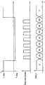
Schematically show actuator device among Fig. 1, this actuator device is represented with Reference numeral 10.Driving arrangement 10 can be used for having enhancing the control possibility the general lighting lamp or be used for pixelation (pixelated) lamp, perhaps be used for supporting backlightly adding bright with space deepening or part signage applications.
Especially, in an illustrated embodiment,actuator device 10 is used to control light-emitting component 14, and these light-emitting components 14 in series are coupled to form string 16.Light-emitting component 14 is as light emitting diode 15 or Organic Light Emitting Diode (OLED) and be provided.In addition, should be pointed out that each light-emitting component 14 can comprise one or more LED or the OLED that is provided with series, parallel or its combination.In the following description, express the light-emitting component 14 of LED 15 general expression mentioned kinds.
Power supply 18 is to LED 15 power supplies ofLED string 16, and power supply 18 for example is a current source 19.This current source can be controlled via the control signal that offerscontrol input 17.
To each the LED 15 distribution module circuit 12.1-12.n in theLED string 16, these modularized circuits are used for controlling LED 15 separately.The quantity of the modularized circuit 12 that is provided is corresponding to the quantity of the light-emitting component 14 that forms thisLED string 16.
Because modularized circuit 12.1-12.n constitutes in a similar fashion, therefore following description only relates to a modularized circuit, and promptly modularized circuit 12.2.
Modularized circuit 12.2 comprises thediverting switch 22 with LED 15 parallel coupled.If should break off LED 15,diverting switch 22 is used for establishing bypass to this LED15 so.If desirable is this LED emission light, opens so and promptly break offcorresponding diverting switch 22, thereby do not have bypass.Therefore, thus the power that is provided can arrive LED 15 produces optical radiation.
The control of divertingswitch 22 controlledunit 24, this control module offersdiverting switch 22 with control signal via control signal wire 26.In addition, thus a side ofcontrol module 24 and divertingswitch 22 and havepublic reference potential 28 with the cathode side electric coupling of LED 15.
Register 30 is suitable for forming withother registers 30 of modularized circuit 12.1-12.n the one-level of serial-to-parallel converter 31.
In order to realize the serial-to-parallel converter, eachregister 30 all has Data_in (data input) input and clock input, and exports as the data_out (data output) of the control signal on the control signal wire 26.As well known by persons skilled in the art, the serial data stream that offers the serial-to-parallel converter moves with each clock signal step by step.
With reference to the embodiment shown in the figure 1, serial data stream is provided for first modularized circuit 12.1, then this serial data stream is sent to the modularized circuit 12.2-12.n of back.Therefore, n clock signal used in the input of n data values.
In order to make serial data stream be delivered to next modularized circuit from a modularized circuit, these modularized circuits haveData_in port 33 and Clock_and_Supply (clock and power supply) port 35.In addition, each modularized circuit 12 all hasData_out port 43 andClock_and_Supply output port 45.
As conspicuous from Fig. 1, theData_in port 33 of modularized circuit andData_out port 43 electric coupling of previous modularized circuit.In addition,Clock_and_Supply output port 45 electric coupling ofClock_and_Supply input port 35 and previous modularized circuit 12.
Each port that also shows modularized circuit among Fig. 1 connects vialine
As previously mentioned,control module 24 compriseslevel moving meter 32, and this is essential, because the electromotive force ofRP 28 is according to the state (on/off) of the position of modularized circuit corresponding in theLED string 16 and LED and difference.The level moving meter of each modularized circuit 12 guarantees that divertingswitch 22 can be switched on and break off, although the reference potential of corresponding LED floats.Level moving meter 32 guarantees that the electromotive force of the control output ofRP 28 and said register 30 (be not) to raise during programming mode during the normal running.
As conspicuous equally from Fig. 1; Each modularized circuit all comprises twoLED ports string 16.
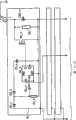
With reference to figure 2, it shows the preferred embodiment ofequipment 10, and will at length describe below.Owing to modularized circuit 12.1-12.n has been carried out similar design, therefore will describe the structure of modularized circuit 12.2 now in detail.
Theregister 30 that provides is forms of so-called D-latch 44, and it generally is known in the art.D-latch 44 has data output Q, and the grid of MOSFET42 is coupled in this data output.The data-in port D of D-latch 44 is connected withData_in port 33 to receive the data output of previous circuit (being modularized circuit 12.1) here.
Two diode D1_2, D2_2 and the capacitor C1_2 of series connection are provided between the Clock_and_Supply of modularized circuit 12.2port 35 and RP 28.Bridge contact between these two diode D1_2 and the D2_2 is connected to phase inverter A2_2, and the output of this phase inverter A2_2 is connected to the clock input CLK of D-latch 44.In addition, resistor R 1_2 is coupling between this bridge contact and the RP 28.At last, the CLR of D-latch 44 input also is connected toRP 28.
As a kind of interchangeable scheme, PRE-Input (PRE input) or CLR-Input (CLR input) can be connected to the pulse forming network that obtains pulse when positive voltage appears in bridge contact place between D1_n and D2_2.This will cause automatically closed or open this switch, and therefore automatically this state spread all over whole being connected in series.Utilize the charging of the regulation of initial state that this scheme can have a regulation that is used for each data transmission and all capacitor C1_n.
The signal that puts onClock_and_Supply output port 45 obtains from the bridge contact between diode D1_2 and the D2_2.
The Clock_and_Supply input port of modularized circuit 12.2 is via the anode coupling ofClock_and_Supply line 36 with diode D1_2.
In order to set up the serial-to-parallel converter, the output signal of D-latch 44 (being Q signal) offersData_out port 43 via resistor R 2_2, and thisData_out port 43 itself is connected to theData_in port 33 of next modularized circuit 12.3.At last, betweenData_out port 43 andRP 28, capacitor C2_2 is provided.This capacitor C2_2 is used for the dedicated delay that signal is propagated.Based on the speed of employed logical device, can it be omitted.
Generally speaking, the outputDriven MOSFET 42 of D-latch 44.Signal (low or high) according to D-latch 44 is switched on or switched off this MOSFET.Capacitor C1_2 is provided so that the supply voltage of corresponding modularized circuit 12 is stable.This supply voltage is as the reference voltage of the cathode side (RP 28) of LED 15.Utilize diode D1_2 and D2_2 and pull down resistor R1_2, obtain putting on the clock signal part of the Clock_and_Supply signal ofport 35 owing to decoupling.
The operation of the drivingarrangement 10 shown in Fig. 2 is following:
During being used for the programming mode that the D-latch 44 of correspondence is programmed, force negative current I1<0 through said circuit, and the suitable control signal that 17 places are imported in its control by current source causes.Therefore, according to the state of previous switch, perhaps MOSFET is along the opposite direction conducting, the perhaps body diode conducting of theMOSFET 42 of modularized circuit 12.Under any situation, all break off all LED 15.When utilizing above-mentioned pulse forming network to remove latch (utilizing CLR-input), can realize situation about hereinafter describing.With positive voltage VCcPut on theClock_and_Supply port 35 of first modularized circuit 12.1.Via diode D1_1...D2_n, the supply voltage capacitor (C1_n) of these modules is recharged
Vsupply=Vcc-Vf
V whereinfIt is the forward voltage of the used diode type of D2_x.This supply voltage almost equates for each modularized circuit.According to diode type and the negative current I used to D1_x1Suitable selection, the voltage drop at the body diode two ends ofMOSFET 42 is identical with the voltage drop at diode D1_x two ends, so they are cancelled out each other.
At each clock input CLK (at the R1_x two ends), there is high level.
Then, benchmark (datum) (controlling value) is put on theData_in port 33 of first modularized circuit 12.1.And then, the Clock_and_Supply signal is set to 0V.Like this, the data (Data_in) of input place of each modularized circuit are copied to the output of each D-latch 44.Because with the speed delay associated of logic (by RC network R2_x, C2_x representative or forms), each modularized circuit all copies to it with the data of the falling edge existence of Clock_and_Supply port and exports Q with intentionallying.
Certainly, between two adjacent modular circuit that send and receive shifted data, there is electric potential difference.But should change the voltage drop that (shift) can not surpass an individual diodes (~0.5V).Can be easy to pronounced high level from piece x+1 (V for example from the high level of modularized circuit 12.x outputCc=5V, CMOS_ height=4.95V will cause the input signal of 5.45V for the modularized circuit on top).For the modularized circuit on top, and low level (CMOS_ is low=and 0.05V) will be 0.45V.Usually, all logical device all have from the Signal Terminal to the power supply catching diode with reference potential.Utilize simple current-limiting resistor (the for example R2_x shown in Fig. 2) will allow safety and stable operation.
Then, the Clock_and_Supply signal withport 35 places of modularized circuit 12.1 is set to V once moreCcNew benchmark is put on theData_in port 33 of this modularized circuit 12.1.Repeat above-mentioned circulation, and on other modularized circuits 12.2-12.n, make the serial data stream parallelization atData_in port 33 places of modularized circuit 12.1.At each negative edge of Clock_and_Supply input signal, make and move a modularized circuit on these data, mean from 12.x to 12.x+1.
At that time clock system (clocked) all desired information in latch 44 time (normally after n clock period, at this moment having upgraded all latchs), Clock_and_Supply imports and remains on 0V.
Then, put on current source 18 and this current source is arranged to positive current I through control signal correspondence1>0 leaves programming mode, and said positive current is the desirable forward current of LED 15.In each piece, if " 0 " and theMOSFET 42 of storage open in latch 44, electric current I so1To flow through LED 15, if perhaps latch 44 is programmed for " 1 ", this electric current I so1To flow throughMOSFET 42.
Owing among the LED 15 or the forward current among theMOSFET 42, will have positive voltage drop at each modularized circuit two ends.In any case do not monitor in the input voltage range that this data-signal and this data-signal all allowing or owing to above-mentioned current-limiting resistor R2_x is protected in this operating period.Allreference potentials 28 all are positive with respect to GND, and therefore the Clock_and_Supply signal is low (or negative) for each modularized circuit.Negative voltage is stopped by diode D1_x.In the clock input of said actuator device, do not have transformation, and the latch information in the latch 44 keeps stable.
Variation for the state of LED repeats aforesaid whole circulation, and promptly with the beginning that is provided with of negative current, the back is that clock control (clocking) new data is in this structure.
Fig. 3 shows above-mentioned programmed sequence, is example with 7 modularized circuit 12.1-12.7.When electric current is arranged to I1>0 o'clock, LED_1...LED_n was according to inverted data D6...D0 and luminous.The length of clock pulse interval is adjusted with the quantity of LED.When generating a Clock_and_Supply signal and several data_in signal simultaneously, data source can be controlled several LED strings 16.That kind can easily be controlled the display lighting element.
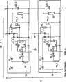
Illustrate the embodiment that revises a little ofactuator device 10 shown in Figure 2 among Fig. 4.Main difference is that the Clock_and_Supply signal is set to all modularized circuit 12.1-12.n parallel.Therefore, these modularized circuits 12 no longer have Clock_and_Supply output port 45.In other words, the Clock_and_Supply signal gets into each modularized circuit but after D1_X, can not leave (leave) each modularized circuit.This causes Potential Distributing different slightly during programming mode.In this case, during programming, need place bypassedresistor 52 and current source at the LED15 two ends and be set to 0 (and not being set to negative current).
As mentioned; Actuator device of the present invention is as the control possibility that strengthens and applicable to producing illuminating lamp; Perhaps as Core Feature and applicable to the pixelation lamp, perhaps applicable to supporting space deepening or part in backlight and the signage applications to add bright.
Claims (11)
1. one kind is used for the equipment of the OLED/LED element of driving OLED/LED string individually, and said equipment all comprises modular unit (12.1-12.n) for each OLED/LED element of said OLED/LED string, and each modular unit all comprises:
Controllable diverting switch (22,42), itself and corresponding OLED/LED element (14,15) coupling,
On-off controller device (30,44), it is used to control said diverting switch (22,42) and has control output end mouth, data-in port and the input end of clock mouth that is coupled to said switch (22,42), and
Level moving device (32); It is distributed to said on-off controller device (30,44) and is suitable for during programming mode, making control input data to reach is enough to the level of being accepted by said on-off controller device (30,44) and allows the said diverting switch (22 of control; 42)
The said on-off controller device (30 of wherein said modular unit (12.1-12.n); 44) thus in series coupling moves to said control input data the on-off controller device (30,44) of corresponding modular unit subsequently and forms serial-to-parallel converter apparatus (31).
2. equipment according to claim 1 is characterized in that, when through serial data stream said on-off controller device (30,44) when programming, being broken off said diverting switch (22,42).
3. equipment according to claim 1 and 2 is characterized in that, said diverting switch (22,42) is transistor (42).
4. equipment according to claim 1 and 2 is characterized in that, said diverting switch (22,42) is a field effect transistor.
5. equipment according to claim 1 and 2 is characterized in that, said on-off controller device (30,44) is the D-latch device (44) that triggers via said input end of clock mouth (CLK).
6. equipment according to claim 5; It is characterized in that; Said level moving device (32) is included in that provide and capacitor series coupled (C1_x) and first diode (D2_x) between potential reference point (28) and its clock input port (CLK) of said latch devices (44); Wherein during the said serial-to-parallel converter apparatus (31) that is formed by said on-off controller device is programmed, to said input end of clock mouth clock and power supply signal are provided via second diode (D1_x).
7. equipment according to claim 5 is characterized in that, the said data-in port (D) of latch devices (44) is coupled so that form said serial-to-parallel converter (31) with the said output port of previous latch.
8. equipment according to claim 7 is characterized in that, between the data-out port (Q) of the data-in port (D) of said latch devices (44) and said previous latch devices, current-limiting resistor (R2_x) is provided.
9. equipment according to claim 6 is characterized in that, the input end of clock mouth (CLK) that inverter apparatus (A2_x) is distributed to each latch devices (44) is so that with said clock input signal anti-phase.
10. equipment according to claim 6 is characterized in that, said clock and power supply signal are provided by second diode (D1_x) of previous level moving device.
11. equipment according to claim 6; It is characterized in that, said clock and power supply signal are offered second diode (D1_x) of each level moving device, and give each OLED/LED element (14; 15) distribute resistor (52), it is used as bypass during programming.
Applications Claiming Priority (3)
| Application Number | Priority Date | Filing Date | Title |
|---|---|---|---|
| EP07106833.2 | 2007-04-24 | ||
| EP07106833 | 2007-04-24 | ||
| PCT/IB2008/051520WO2008129504A1 (en) | 2007-04-24 | 2008-04-21 | Led string driver with shift register and level shifter |
Publications (2)
| Publication Number | Publication Date |
|---|---|
| CN101669404A CN101669404A (en) | 2010-03-10 |
| CN101669404Btrue CN101669404B (en) | 2012-03-28 |
Family
ID=39535197
Family Applications (1)
| Application Number | Title | Priority Date | Filing Date |
|---|---|---|---|
| CN2008800136856AActiveCN101669404B (en) | 2007-04-24 | 2008-04-21 | LED string driver with shift register and level shifter |
Country Status (7)
| Country | Link |
|---|---|
| US (1) | US8159454B2 (en) |
| EP (1) | EP2143304B1 (en) |
| JP (1) | JP5519490B2 (en) |
| CN (1) | CN101669404B (en) |
| AT (1) | ATE481854T1 (en) |
| DE (1) | DE602008002579D1 (en) |
| WO (1) | WO2008129504A1 (en) |
Families Citing this family (63)
| Publication number | Priority date | Publication date | Assignee | Title |
|---|---|---|---|---|
| US20050259424A1 (en) | 2004-05-18 | 2005-11-24 | Zampini Thomas L Ii | Collimating and controlling light produced by light emitting diodes |
| US7766511B2 (en) | 2006-04-24 | 2010-08-03 | Integrated Illumination Systems | LED light fixture |
| US7729941B2 (en) | 2006-11-17 | 2010-06-01 | Integrated Illumination Systems, Inc. | Apparatus and method of using lighting systems to enhance brand recognition |
| US8013538B2 (en) | 2007-01-26 | 2011-09-06 | Integrated Illumination Systems, Inc. | TRI-light |
| US8742686B2 (en) | 2007-09-24 | 2014-06-03 | Integrated Illumination Systems, Inc. | Systems and methods for providing an OEM level networked lighting system |
| CN101878673B (en)* | 2007-11-30 | 2014-02-12 | 皇家飞利浦电子股份有限公司 | light output device |
| US8255487B2 (en) | 2008-05-16 | 2012-08-28 | Integrated Illumination Systems, Inc. | Systems and methods for communicating in a lighting network |
| US9801243B2 (en) | 2008-11-13 | 2017-10-24 | Philips Lighting Holding B.V. | Lighting system with a plurality of LEDs |
| CN102349354A (en)* | 2009-02-17 | 2012-02-08 | 鲁米自然株式会社 | Power-saving led lighting apparatus |
| US8585245B2 (en) | 2009-04-23 | 2013-11-19 | Integrated Illumination Systems, Inc. | Systems and methods for sealing a lighting fixture |
| US9713211B2 (en) | 2009-09-24 | 2017-07-18 | Cree, Inc. | Solid state lighting apparatus with controllable bypass circuits and methods of operation thereof |
| US8901829B2 (en) | 2009-09-24 | 2014-12-02 | Cree Led Lighting Solutions, Inc. | Solid state lighting apparatus with configurable shunts |
| US10264637B2 (en) | 2009-09-24 | 2019-04-16 | Cree, Inc. | Solid state lighting apparatus with compensation bypass circuits and methods of operation thereof |
| US8901845B2 (en) | 2009-09-24 | 2014-12-02 | Cree, Inc. | Temperature responsive control for lighting apparatus including light emitting devices providing different chromaticities and related methods |
| US9285103B2 (en) | 2009-09-25 | 2016-03-15 | Cree, Inc. | Light engines for lighting devices |
| US9068719B2 (en) | 2009-09-25 | 2015-06-30 | Cree, Inc. | Light engines for lighting devices |
| US8602579B2 (en) | 2009-09-25 | 2013-12-10 | Cree, Inc. | Lighting devices including thermally conductive housings and related structures |
| US8777449B2 (en) | 2009-09-25 | 2014-07-15 | Cree, Inc. | Lighting devices comprising solid state light emitters |
| CN102076139B (en)* | 2009-11-19 | 2013-12-11 | 群康科技(深圳)有限公司 | LED lighting circuit |
| US8476836B2 (en) | 2010-05-07 | 2013-07-02 | Cree, Inc. | AC driven solid state lighting apparatus with LED string including switched segments |
| JP5894982B2 (en)* | 2010-07-09 | 2016-03-30 | コーニンクレッカ フィリップス エヌ ヴェKoninklijke Philips N.V. | Management circuit for organic light-emitting diodes |
| US9295124B2 (en) | 2010-07-30 | 2016-03-22 | Infineon Technologies Americas Corp. | System using shunt circuits to selectively bypass open loads |
| CN102348304A (en)* | 2010-08-03 | 2012-02-08 | 镇江市亿华系统集成有限公司 | Light-emitting diode batch dimming and switch control combined circuit |
| IL208830A (en)* | 2010-10-20 | 2016-08-31 | Krupkin Vladimir | Laser jammer |
| US9066381B2 (en) | 2011-03-16 | 2015-06-23 | Integrated Illumination Systems, Inc. | System and method for low level dimming |
| US8599891B2 (en)* | 2011-03-21 | 2013-12-03 | Soreq Nuclear Research Center | Laser diode driver |
| US9967940B2 (en) | 2011-05-05 | 2018-05-08 | Integrated Illumination Systems, Inc. | Systems and methods for active thermal management |
| US9839083B2 (en) | 2011-06-03 | 2017-12-05 | Cree, Inc. | Solid state lighting apparatus and circuits including LED segments configured for targeted spectral power distribution and methods of operating the same |
| US9521725B2 (en) | 2011-07-26 | 2016-12-13 | Hunter Industries, Inc. | Systems and methods for providing power and data to lighting devices |
| US8710770B2 (en) | 2011-07-26 | 2014-04-29 | Hunter Industries, Inc. | Systems and methods for providing power and data to lighting devices |
| US11917740B2 (en) | 2011-07-26 | 2024-02-27 | Hunter Industries, Inc. | Systems and methods for providing power and data to devices |
| US20150237700A1 (en) | 2011-07-26 | 2015-08-20 | Hunter Industries, Inc. | Systems and methods to control color and brightness of lighting devices |
| US10874003B2 (en) | 2011-07-26 | 2020-12-22 | Hunter Industries, Inc. | Systems and methods for providing power and data to devices |
| US9609720B2 (en) | 2011-07-26 | 2017-03-28 | Hunter Industries, Inc. | Systems and methods for providing power and data to lighting devices |
| US9131561B2 (en) | 2011-09-16 | 2015-09-08 | Cree, Inc. | Solid-state lighting apparatus and methods using energy storage |
| US9277605B2 (en) | 2011-09-16 | 2016-03-01 | Cree, Inc. | Solid-state lighting apparatus and methods using current diversion controlled by lighting device bias states |
| US8742671B2 (en) | 2011-07-28 | 2014-06-03 | Cree, Inc. | Solid state lighting apparatus and methods using integrated driver circuitry |
| US9125263B2 (en) | 2011-08-05 | 2015-09-01 | Mitsubishi Electric Corporation | LED lighting device |
| WO2013022434A1 (en)* | 2011-08-09 | 2013-02-14 | Universal Display Corporation | Light emitters with series connection |
| US8791641B2 (en) | 2011-09-16 | 2014-07-29 | Cree, Inc. | Solid-state lighting apparatus and methods using energy storage |
| JP5870294B2 (en)* | 2011-11-30 | 2016-02-24 | パナソニックIpマネジメント株式会社 | Organic EL element lighting device and lighting apparatus using the same |
| DK177534B1 (en) | 2012-03-21 | 2013-09-08 | Martin Professional As | Flexible led pixel string with two shielding ground lines |
| WO2013160787A1 (en)* | 2012-04-23 | 2013-10-31 | Koninklijke Philips N.V. | Separately controllable array of radiation elements |
| US8894437B2 (en) | 2012-07-19 | 2014-11-25 | Integrated Illumination Systems, Inc. | Systems and methods for connector enabling vertical removal |
| US9379578B2 (en) | 2012-11-19 | 2016-06-28 | Integrated Illumination Systems, Inc. | Systems and methods for multi-state power management |
| DE102012111247A1 (en) | 2012-11-21 | 2014-05-22 | Osram Opto Semiconductors Gmbh | Optoelectronic semiconductor device |
| US9420665B2 (en) | 2012-12-28 | 2016-08-16 | Integration Illumination Systems, Inc. | Systems and methods for continuous adjustment of reference signal to control chip |
| US9485814B2 (en) | 2013-01-04 | 2016-11-01 | Integrated Illumination Systems, Inc. | Systems and methods for a hysteresis based driver using a LED as a voltage reference |
| US9095026B2 (en)* | 2014-01-02 | 2015-07-28 | Semiconductor Components Industries, Llc | LED controller and method therefor |
| US10228711B2 (en) | 2015-05-26 | 2019-03-12 | Hunter Industries, Inc. | Decoder systems and methods for irrigation control |
| US10918030B2 (en) | 2015-05-26 | 2021-02-16 | Hunter Industries, Inc. | Decoder systems and methods for irrigation control |
| US10030844B2 (en) | 2015-05-29 | 2018-07-24 | Integrated Illumination Systems, Inc. | Systems, methods and apparatus for illumination using asymmetrical optics |
| US10060599B2 (en) | 2015-05-29 | 2018-08-28 | Integrated Illumination Systems, Inc. | Systems, methods and apparatus for programmable light fixtures |
| CN104966488A (en)* | 2015-06-30 | 2015-10-07 | 陶象余 | One-fourth scanning LED display drive circuit |
| EP3145277B1 (en) | 2015-09-17 | 2020-11-11 | Nxp B.V. | Circuits, controllers and methods for controlling led strings or circuits |
| US10201044B2 (en)* | 2015-10-27 | 2019-02-05 | Abl Ip Holding Llc | Modular light-emitting diode fixtures |
| FR3046294A1 (en)* | 2015-12-29 | 2017-06-30 | Aledia | OPTOELECTRONIC CIRCUIT WITH ELECTROLUMINESCENT DIODES |
| US10068529B2 (en)* | 2016-11-07 | 2018-09-04 | International Business Machines Corporation | Active matrix OLED display with normally-on thin-film transistors |
| US10009973B1 (en)* | 2017-03-06 | 2018-06-26 | Usai, Llc | Redundant power for lighting system |
| US9967946B1 (en) | 2017-08-14 | 2018-05-08 | Nxp B.V. | Overshoot protection circuit for LED lighting |
| US10801714B1 (en) | 2019-10-03 | 2020-10-13 | CarJamz, Inc. | Lighting device |
| US12416908B2 (en) | 2022-12-29 | 2025-09-16 | Integrated Illumination Systems, Inc. | Systems and methods for manufacturing light fixtures |
| US12297996B2 (en) | 2023-02-16 | 2025-05-13 | Integrated Illumination Systems, Inc. | Cove light fixture with hidden integrated air return |
Family Cites Families (24)
| Publication number | Priority date | Publication date | Assignee | Title |
|---|---|---|---|---|
| JPH075837A (en)* | 1993-06-15 | 1995-01-10 | De-Shisu:Kk | Information display device |
| JP2788401B2 (en)* | 1993-11-09 | 1998-08-20 | 小糸工業株式会社 | Display device |
| CA2177167A1 (en)* | 1994-09-27 | 1996-04-04 | Shinsuke Nishida | Display device |
| JPH08194439A (en)* | 1995-01-18 | 1996-07-30 | Nippon Dennetsu Co Ltd | Light-emitting diode display device |
| US6297787B1 (en)* | 1996-01-11 | 2001-10-02 | Fourie, Inc. | Display device |
| US6777891B2 (en) | 1997-08-26 | 2004-08-17 | Color Kinetics, Incorporated | Methods and apparatus for controlling devices in a networked lighting system |
| JP4014715B2 (en)* | 1997-12-26 | 2007-11-28 | アビックス株式会社 | LED illumination unit and LED illumination system |
| EP0967590A1 (en)* | 1998-06-25 | 1999-12-29 | Hewlett-Packard Company | Optical display device using LEDs and its operating method |
| JP2000098964A (en)* | 1998-09-18 | 2000-04-07 | Stanley Electric Co Ltd | Information display device |
| US6153980A (en) | 1999-11-04 | 2000-11-28 | Philips Electronics North America Corporation | LED array having an active shunt arrangement |
| JP4491872B2 (en)* | 1999-11-30 | 2010-06-30 | 日亜化学工業株式会社 | LED display device |
| JP2001312246A (en)* | 2000-05-01 | 2001-11-09 | Sony Corp | Modulation circuit and image display device using the same |
| JP2001350439A (en)* | 2000-06-06 | 2001-12-21 | Sony Corp | Modulation circuit and picture display device using the same |
| JP2002108286A (en)* | 2000-09-28 | 2002-04-10 | Nichia Chem Ind Ltd | Display device and drive control system |
| DE10103611B4 (en)* | 2001-01-26 | 2013-12-19 | Insta Elektro Gmbh | Circuit arrangement for operating a plurality of bulbs |
| DE10159765C2 (en) | 2001-12-05 | 2003-11-06 | Audi Ag | Arrangement for controlling a number of light-emitting diodes and method for operating such an arrangement |
| US20040090403A1 (en) | 2002-11-08 | 2004-05-13 | Dynascan Technology Corp. | Light-emitting diode display apparatus with low electromagnetic display |
| DE10358447B3 (en)* | 2003-12-13 | 2005-05-25 | Insta Elektro Gmbh | Illumination device has series LEDs, each with parallel-connected electronic unit with low impedance switch element, diode, threshold switch, capacitor whose voltage supplies threshold switch and is fed to threshold switch as its input |
| US7505395B2 (en) | 2004-04-19 | 2009-03-17 | Tir Technology Lp | Parallel pulse code modulation system and method |
| JP4720099B2 (en)* | 2004-04-20 | 2011-07-13 | ソニー株式会社 | Constant current drive device, backlight light source device, and color liquid crystal display device |
| US20060038803A1 (en)* | 2004-08-20 | 2006-02-23 | Semiconductor Components Industries, Llc | LED control method and structure therefor |
| US7126623B2 (en) | 2004-12-15 | 2006-10-24 | Star-Reach Corporation | Serially connected LED lamps control device |
| CA2768198C (en)* | 2005-04-08 | 2013-11-26 | Eldolab Holding B.V. | Methods and apparatuses for operating groups of high-power leds |
| US7649326B2 (en)* | 2006-03-27 | 2010-01-19 | Texas Instruments Incorporated | Highly efficient series string LED driver with individual LED control |
- 2008
- 2008-04-21CNCN2008800136856Apatent/CN101669404B/enactiveActive
- 2008-04-21USUS12/596,484patent/US8159454B2/enactiveActive
- 2008-04-21EPEP08737928Apatent/EP2143304B1/enactiveActive
- 2008-04-21DEDE602008002579Tpatent/DE602008002579D1/enactiveActive
- 2008-04-21ATAT08737928Tpatent/ATE481854T1/ennot_activeIP Right Cessation
- 2008-04-21JPJP2010504932Apatent/JP5519490B2/enactiveActive
- 2008-04-21WOPCT/IB2008/051520patent/WO2008129504A1/enactiveApplication Filing
Also Published As
| Publication number | Publication date |
|---|---|
| EP2143304B1 (en) | 2010-09-15 |
| ATE481854T1 (en) | 2010-10-15 |
| CN101669404A (en) | 2010-03-10 |
| DE602008002579D1 (en) | 2010-10-28 |
| JP5519490B2 (en) | 2014-06-11 |
| EP2143304A1 (en) | 2010-01-13 |
| US20100134041A1 (en) | 2010-06-03 |
| WO2008129504A1 (en) | 2008-10-30 |
| US8159454B2 (en) | 2012-04-17 |
| JP2010527459A (en) | 2010-08-12 |
Similar Documents
| Publication | Publication Date | Title |
|---|---|---|
| CN101669404B (en) | LED string driver with shift register and level shifter | |
| US8378591B2 (en) | Light output device | |
| CN105976766B (en) | Back light unit and its driving method, and use its liquid crystal display device | |
| CN100399398C (en) | Charge and discharge control circuit, light emitting device and driving method thereof | |
| CN100581307C (en) | light emitting device | |
| CN107493635A (en) | A kind of more pixel drive systems of LED | |
| CN104106315A (en) | Led matrix manager | |
| CN102214432A (en) | Power management and control module and liquid crystal display | |
| CN107481661A (en) | The operating method and display device of display device | |
| KR101952635B1 (en) | Light Emitting Diode Driving Circuit | |
| CN103379687A (en) | Semiconductor circuit and semiconductor apparatus | |
| CN109686319A (en) | The super more backlight subarea drive control circuits of one kind and display device | |
| WO2005078810A1 (en) | Light source driver circuit, illuminating apparatus, display apparatus, field sequential color system liquid crystal display apparatus, and information device | |
| CN109920368A (en) | A kind of μ LED pixel drive circuit system and driving method | |
| CN102316625B (en) | Lighting device and light source control circuit thereof | |
| CN104247566B (en) | The individually controllable array of radiating element | |
| TW505578B (en) | Self-scanning light-emitting device | |
| CN108831375A (en) | A kind of pixel circuit and its driving method, display device | |
| CN103262147B (en) | Power circuit and employ the display equipment of this power circuit | |
| CN103578413A (en) | Voltage generator, driving method for the voltage generator and organic light emitting display device using the same | |
| CN207321594U (en) | A kind of more pixel drive systems of LED | |
| KR20110060053A (en) | Driving device and driving method of light emitting diode array | |
| CN100562911C (en) | Light emitting diode driver and display device using the same | |
| CN113498234B (en) | MOS tube driving circuit and enhanced LED driving circuit | |
| CN113129807B (en) | Light emitting diode pixel display unit, light emitting diode display device and brightness adjusting method thereof |
Legal Events
| Date | Code | Title | Description |
|---|---|---|---|
| C06 | Publication | ||
| PB01 | Publication | ||
| C10 | Entry into substantive examination | ||
| SE01 | Entry into force of request for substantive examination | ||
| C14 | Grant of patent or utility model | ||
| GR01 | Patent grant | ||
| CP01 | Change in the name or title of a patent holder | ||
| CP01 | Change in the name or title of a patent holder | Address after:Holland Ian Deho Finn Patentee after:KONINKLIJKE PHILIPS N.V. Address before:Holland Ian Deho Finn Patentee before:Koninklijke Philips Electronics N.V. | |
| TR01 | Transfer of patent right | ||
| TR01 | Transfer of patent right | Effective date of registration:20170310 Address after:The city of Eindhoven in Holland Patentee after:PHILIPS LIGHTING HOLDING B.V. Address before:Holland Ian Deho Finn Patentee before:KONINKLIJKE PHILIPS N.V. | |
| CP03 | Change of name, title or address | ||
| CP03 | Change of name, title or address | Address after:Eindhoven Patentee after:Signify Holdings Ltd. Address before:The city of Eindhoven in Holland Patentee before:PHILIPS LIGHTING HOLDING B.V. |