CN101669226A - Long-life phosphorescent Organic Light Emitting Device (OLED) structures - Google Patents
Long-life phosphorescent Organic Light Emitting Device (OLED) structuresDownload PDFInfo
- Publication number
- CN101669226A CN101669226ACN200780050827ACN200780050827ACN101669226ACN 101669226 ACN101669226 ACN 101669226ACN 200780050827 ACN200780050827 ACN 200780050827ACN 200780050827 ACN200780050827 ACN 200780050827ACN 101669226 ACN101669226 ACN 101669226A
- Authority
- CN
- China
- Prior art keywords
- organic layer
- emissive
- phosphorescent
- concentration
- phosphorescent material
- Prior art date
- Legal status (The legal status is an assumption and is not a legal conclusion. Google has not performed a legal analysis and makes no representation as to the accuracy of the status listed.)
- Pending
Links
Images


Landscapes
- Electroluminescent Light Sources (AREA)
Abstract
Description
Translated fromChinese本申请要求2006年12月28日提交的美国临时申请60/877,696和2007年2月8日提交的美国临时申请60/900,624的优先权,所述临时申请通过引用整体结合到本申请中。This application claims priority to US
所要求保护的本发明代表一个或多个如下联合的大学公司研究协议当事人和/或与这些当事人相关而完成的:密西根大学、普林斯顿大学、南加州大学和the Universal Display Corporation的董事。所述协议在所要求保护的本发明完成日和之前是有效的,并且所要求保护的发明是作为在所述协议的范围内采取行动的结果而完成的。The claimed invention was made on behalf of and/or in connection with one or more of the following parties to a joint university-corporate research agreement: Regents of the University of Michigan, Princeton University, University of Southern California, and the Universal Display Corporation. The agreement was in effect on and before the date the claimed invention was made, and the claimed invention was made as a result of actions taken within the scope of the agreement.
发明领域field of invention
本发明涉及有机发光器件(OLEDs)。更具体地说,本发明涉及具有可提高寿命的特定结构的OLEDs。The present invention relates to organic light emitting devices (OLEDs). More specifically, the present invention relates to OLEDs having a specific structure that improves lifetime.
发明背景Background of the invention
利用有机材料的光电器件由于许多原因越来越为人们所需求。用来制造此类器件的许多材料是相对便宜的,因此有机光电器件具有在成本上比无机器件有优势的可能。此外,有机材料的固有性能如它们的柔性可能使得它们非常适合于特殊应用,如在柔性基材上制造。有机光电器件的实例包括有机发光器件(OLEDs)、有机光敏晶体管、有机光生伏打电池和有机光检测器。对于OLEDs,有机材料可能比常规材料有性能优势。例如,有机发射层发光的波长一般可能容易地用合适的掺杂剂调节。Optoelectronic devices utilizing organic materials are increasingly in demand for a number of reasons. Many of the materials used to fabricate such devices are relatively inexpensive, so organic optoelectronic devices have the potential to offer cost advantages over inorganic devices. Furthermore, the intrinsic properties of organic materials such as their flexibility may make them well suited for specialized applications such as fabrication on flexible substrates. Examples of organic optoelectronic devices include organic light emitting devices (OLEDs), organic phototransistors, organic photovoltaic cells, and organic photodetectors. For OLEDs, organic materials may have performance advantages over conventional materials. For example, the wavelength at which an organic emissive layer emits light can generally be easily tuned with suitable dopants.
OLEDs利用薄的有机膜,当对器件施加电压时所述有机膜会发光。OLEDs正在成为人们越来越感兴趣的技术,用于诸如平板显示器、照明和逆光照明之类的应用中。几种OLED材料和结构已被描述在美国专利5,844,363、6,303,238和5,707,745中,它们的全部内容通过引用结合在本文中。OLEDs utilize thin organic films that emit light when a voltage is applied to the device. OLEDs are becoming an increasingly interesting technology for applications such as flat panel displays, lighting and backlighting. Several OLED materials and structures have been described in US Patents 5,844,363, 6,303,238, and 5,707,745, the entire contents of which are incorporated herein by reference.
磷光发射分子的一种应用是全色显示器。这样的显示器的工业标准需要适合发射被称为“饱和”色的特定色光的像素。特别地,这些标准需要饱和的红、绿和蓝像素。可应用本领域熟知的CIE坐标测定颜色。One application of phosphorescent emitting molecules is in full-color displays. The industry standard for such displays requires pixels adapted to emit a particular color of light known as a "saturated" color. In particular, these standards require saturated red, green and blue pixels. Color can be measured using CIE coordinates well known in the art.
发射绿光的分子的一个实例是表示为Ir(ppy)3的三(2-苯基吡啶)合铱,它具有式I的结构:An example of a molecule that emits green light is tris(2-phenylpyridine)iridium, denoted Ir(ppy)3 , which has the structure of formula I:
在该式和本文后面的图中,我们以直线描述从氮到金属(在这里是Ir)的配价键。In this formula and in the figures later in this text, we describe the dative bond from nitrogen to the metal (here Ir) as a straight line.
在本文中使用的术语“有机的”包括可用来制造有机光电器件的聚合物材料和小分子有机材料。“小分子”指不是聚合物的任何有机材料,并且“小分子”实际上可以是相当大的。在一些情况下小分子可包括重复单元。例如,使用长链烷基作为取代基不会将一个分子从“小分子”类型中排除。小分子也可以被引入聚合物中,例如作为聚合物骨架上的侧基或作为骨架的一部分。小分子还可以作为树状分子的芯结构部分,该树状分子由在芯结构部分上构建的一系列化学壳组成。树状分子的芯结构部分可以是荧光或磷光小分子发射体。树状分子可以是“小分子”,并且据信目前在OLED领域中使用的所有树状分子都是小分子。The term "organic" as used herein includes polymeric materials and small molecule organic materials that can be used to fabricate organic optoelectronic devices. "Small molecule" refers to any organic material that is not a polymer, and "small molecules" can actually be quite large. In some cases small molecules may include repeating units. For example, the use of long chain alkyl groups as substituents does not exclude a molecule from the "small molecule" category. Small molecules can also be incorporated into polymers, for example as pendant groups on the polymer backbone or as part of the backbone. Small molecules can also serve as the core moiety of dendrimers, which consist of a series of chemical shells built on top of the core moiety. The core moiety of the dendrimer can be a fluorescent or phosphorescent small molecule emitter. Dendrimers can be "small molecules" and it is believed that all dendrimers currently used in the field of OLEDs are small molecules.
在本文中使用的“顶部”指最远离基材,而“底部”指最接近基材。当第一层被描述为“布置在”第二层上,所述第一层远离基材来设置。在所述第一和第二层之间可以有其它层,除非规定所述第一层与所述第二层“接触”。例如,阴极可以被描述为“布置在”阳极上,即使在两者之间有各种有机层。As used herein, "top" means furthest from the substrate, and "bottom" means closest to the substrate. When a first layer is described as being "disposed on" a second layer, the first layer is disposed away from the substrate. There may be other layers between the first and second layers, unless it is specified that the first layer is "in contact with" the second layer. For example, a cathode can be described as being "disposed over" an anode, even though there are various organic layers in between.
在本文中使用的“可溶液处理的”是指能够在液体介质中溶解、分散或输送和/或从液体介质中沉积,无论呈溶液或悬浮液的形式。As used herein, "solution processable" means capable of being dissolved, dispersed or transported in and/or deposited from a liquid medium, whether in the form of a solution or a suspension.
当据信配位体对发射材料的光活性性能有贡献时,该配位体被称为“光活性的”。A ligand is said to be "photoactive" when it is believed to contribute to the photoactive properties of the emissive material.
如果在常规能级图中第一能级更低,则第一能级(HOMO或LUMO)被认为“小于”或“低于”第二能级,这意味着第一能级将具有比第二能级更负的值。如果在常规能级图中第一能级更高,则第一能级(HOMO或LUMO)被认为“高于”第二能级,这意味着第一能级将具有不如第二能级负的值。例如,CBP的HOMO为-5.32eV,TPBI的HOMO为-5.70eV,因此CBP的HOMO比TPBI的HOMO高0.38eV。类似地,mCP的LUMO是-0.77eV,CBP的LUMO的是-1.23eV,因此mCP的LUMO比CBP的LUMO高0.46eV。上述值使用用可得自Irvine,Calif.的Wavefunction公司的Spartan 02软件包在B3LYP/6-31G*水平进行的密度函数计算确定。赝势选项(pseudo potential option)可以被用于含有重金属的物质如Ir(ppy)3。文献中已证实密度函数计算法能定性地预测有机和无机化合物的能量。A first energy level (HOMO or LUMO) is said to be "less than" or "below" the second energy level if it is lower in a conventional energy level diagram, which means that the first energy level will have a lower The more negative value of the second energy level. A first energy level (HOMO or LUMO) is said to be "higher" than a second energy level if it is higher in a conventional energy level diagram, meaning that the first energy level will have a less negative value. For example, the HOMO of CBP is -5.32eV and the HOMO of TPBI is -5.70eV, so the HOMO of CBP is 0.38eV higher than that of TPBI. Similarly, the LUMO of mCP is -0.77eV and that of CBP is -1.23eV, so the LUMO of mCP is 0.46eV higher than that of CBP. The above values were determined using density function calculations at the B3LYP/6-31G* level with the Spartan 02 software package available from Wavefunction Corporation of Irvine, Calif. The pseudopotential option can be used for heavy metal-containing species such as Ir(ppy)3 . Density function calculations have been demonstrated in the literature to qualitatively predict the energy of organic and inorganic compounds.
有关OLEDs的更多细节和上述定义可见于美国专利7,279,704号,该专利的全文通过引用结合到本文中。Further details regarding OLEDs and the above definitions can be found in US Patent No. 7,279,704, which is hereby incorporated by reference in its entirety.
在本文中使用的术语“基本上由”应用于有机发光器件中的某层的一种或多种材料“组成”意味着除了所列举的那些材料外还可以有材料存在,但是任何这样的另外的材料仅以少量存在(如杂质)并且不显著影响器件的电性能或发射性能,即,它们不显著贡献于空穴或电子的传输或捕获,它们不会导致重组位置的改变,并且它们不显著贡献于或参与激子衰变、发射等。As used herein, the term "consisting essentially of" one or more materials applied to a layer in an organic light-emitting device means that materials other than those listed may also be present, but any such additional materials that exist only in small amounts (such as impurities) and do not significantly affect the electrical or emission properties of the device, that is, they do not significantly contribute to the transport or capture of holes or electrons, they do not cause changes in recombination sites, and they do not Significantly contributes to or participates in excitonic decay, emission, etc.
除非另外指明,本文所描述的各层内的有机化合物的百分数都是重量百分数。Unless otherwise indicated, the percentages of organic compounds in each layer described herein are by weight.
以下两篇包括Samuel作为合著者的文献描述了具有与ITO直接接触的掺杂的发射层的可溶液处理的磷光OLEDs。E.E.Namdas,T.D.Anthopoulos,I.D.W.Samuel,Applied physics letters(应用物理通讯)86,161104(2005)。T.D.Anthopoulos,M.J.Frampton,E.B.Namdas,P.L.Burn,I.D.W.Samuel,Adv.Mater.(材料进展)2004,16,No.6,March 18,pp557-560。The following two papers, including Samuel as a co-author, describe solution-processable phosphorescent OLEDs with a doped emissive layer in direct contact with ITO. E.E. Namdas, T.D. Anthopoulos, I.D.W. Samuel, Applied physics letters (Applied Physics Letters) 86, 161104 (2005). T.D.Anthopoulos, M.J.Frampton, E.B.Namdas, P.L.Burn, I.D.W.Samuel, Adv.Mater. (Advances in Materials) 2004, 16, No.6, March 18, pp557-560.
发明概述Summary of the invention
在第一方面,本发明提供了一种在发射层内有界面的有机发光器件。该器件具有阳极、阴极和布置在阳极和阴极之间的发射层。该发射层包括第一有机层,它包括第一磷光材料和第一非发射材料。所述第一有机层中第一磷光材料的浓度为10-90wt%,且第一有机层中第一非发射材料的浓度为10-90wt%。所述发射层还包括第二有机层,它包括第二磷光材料和第二非发射材料。所述第二层内第二磷光材料的浓度为3-25wt%,且第二有机层中第二非发射材料的浓度为75-97wt%。所述第二有机层中第二磷光材料的浓度比第一有机层中第一磷光材料的浓度低,优选低至少5wt%,更优选低至少10wt%。所述第一非发射材料和所述第二非发射材料可以是相同的材料或不同的材料,并且所述第一磷光材料和所述第二磷光材料可以是相同的材料或不同的材料。因此,有四种组合:(1)第一和第二有机层中的磷光材料相同,并且第一和第二有机层中的非发射材料相同;(2)第一和第二有机层中的磷光材料不同,并且第一和第二有机层中的非发射材料相同;(3)第一和第二有机层中的磷光材料相同,并且第一和第二有机层中的非发射材料不同;(4)第一和第二有机层中的磷光材料不同,并且第一和第二有机层中的非发射材料不同。每种组合都有优点。第一有机层可以基本上由第一磷光材料和第一非发射材料组成,而且第二有机层可以基本上由第一有机层中的第一磷光材料和第一非发射材料组成。本发明还提供了减轻器件中的损伤和延长器件寿命的器件结构,单独地或组合地与第一方面一起使用。In a first aspect, the present invention provides an organic light emitting device having an interface within the emissive layer. The device has an anode, a cathode and an emissive layer arranged between the anode and the cathode. The emissive layer includes a first organic layer that includes a first phosphorescent material and a first non-emissive material. The concentration of the first phosphorescent material in the first organic layer is 10-90wt%, and the concentration of the first non-emitting material in the first organic layer is 10-90wt%. The emissive layer also includes a second organic layer that includes a second phosphorescent material and a second non-emissive material. The concentration of the second phosphorescent material in the second layer is 3-25wt%, and the concentration of the second non-emitting material in the second organic layer is 75-97wt%. The concentration of the second phosphorescent material in the second organic layer is lower than the concentration of the first phosphorescent material in the first organic layer, preferably at least 5 wt%, more preferably at least 10 wt%. The first non-emissive material and the second non-emissive material may be the same material or different materials, and the first phosphorescent material and the second phosphorescent material may be the same material or different materials. Therefore, there are four combinations: (1) the phosphorescent material in the first and second organic layers is the same, and the non-emissive material in the first and second organic layers is the same; (2) the phosphorescent material in the first and second organic layers is the same; The phosphorescent materials are different, and the non-emissive materials in the first and second organic layers are the same; (3) the phosphorescent materials in the first and second organic layers are the same, and the non-emissive materials in the first and second organic layers are different; (4) The phosphorescent materials in the first and second organic layers are different, and the non-emissive materials in the first and second organic layers are different. Each combination has advantages. The first organic layer may consist essentially of the first phosphorescent material and the first non-emissive material, and the second organic layer may consist essentially of the first phosphorescent material and the first non-emissive material in the first organic layer. The present invention also provides a device structure for mitigating damage in the device and prolonging the lifetime of the device, used alone or in combination with the first aspect.
所述第一有机层、所述第二有机层或二者可以任选地进一步包括低能量的发射材料,其中该低能量的发射材料的浓度为0.1-12wt%。The first organic layer, the second organic layer, or both may optionally further include a low-energy emissive material, wherein the low-energy emissive material has a concentration of 0.1-12 wt%.
在第二方面,本发明提供了一种减轻损伤的结构。在所述第一有机层和阳极之间的所有有机层都具有空穴迁移率和电子迁移率,使得空穴迁移率是电子迁移率的至少两倍,优选至少十倍,更优选至少100倍。In a second aspect, the present invention provides a damage mitigating structure. All organic layers between said first organic layer and the anode have hole mobility and electron mobility such that hole mobility is at least twice, preferably at least ten times, more preferably at least 100 times greater than electron mobility .
在第三方面,本发明提供了减轻损伤的另一种结构。在所述第一有机层和阳极之间的所有有机层不包括任何含有选自下组的基团的材料:三芳基胺、萘基、三(N-咔唑基(carbazoyl))三苯基胺、四芳基胺和咔唑。In a third aspect, the present invention provides another structure for mitigating damage. All organic layers between the first organic layer and the anode do not include any material containing a group selected from the group consisting of: triarylamine, naphthyl, tris(N-carbazolyl)triphenyl Amines, tetraarylamines and carbazoles.
在第四方面,本发明提供了减轻损伤的另一种结构。在所述第一有机层和阳极之间无有机层。In a fourth aspect, the present invention provides another structure for mitigating damage. There is no organic layer between the first organic layer and the anode.
在第五方面,本发明提供了减轻损伤的另一种结构。提供了布置在所述第一有机层和阳极之间的第三有机层。该第三有机层基本上由第一磷光材料组成。该第三有机层直接与所述第一有机层和阳极接触,这样它是在所述第一有机层和阳极之间唯一的层。In a fifth aspect, the present invention provides another structure for mitigating damage. A third organic layer disposed between the first organic layer and the anode is provided. The third organic layer consists essentially of the first phosphorescent material. This third organic layer is in direct contact with the first organic layer and the anode such that it is the only layer between the first organic layer and the anode.
在第六方面,本发明提供了减轻损伤的另一种结构。所述器件包括不多于三种不同的有机材料,将受损伤的材料的数目最小化。In a sixth aspect, the present invention provides another structure for mitigating damage. The device includes no more than three different organic materials, minimizing the number of damaged materials.
在第七方面,本发明提供了减轻损伤的另一种结构。所述器件包括不多于四种不同的有机材料,其中所述有机材料之一是仅存在于器件的发射层和阴极之间的电子传输材料。对材料数目的限制将受损伤的材料的数目最小化。In a seventh aspect, the present invention provides another structure for mitigating damage. The device includes no more than four different organic materials, wherein one of the organic materials is an electron transport material present only between the emissive layer and the cathode of the device. Limiting the number of materials minimizes the number of damaged materials.
在第八方面,本发明提供了减轻损伤的另一种结构。在所述第一有机层和阳极之间的所有有机层基本上由有机金属材料组成。In an eighth aspect, the present invention provides another structure for mitigating damage. All organic layers between said first organic layer and the anode consist essentially of organometallic materials.
在第九方面,本发明提供了减轻损伤的另一种结构。在所述第一有机层和阳极之间的所有有机层具有足够大的空穴传导率,使得该层增加10nm厚度导致在10mA/cm2的电流密度下0.1V或更小的电压升高。In a ninth aspect, the present invention provides another structure for reducing damage. All organic layers between the first organic layer and the anode have sufficiently large hole conductivity such that an increase in thickness of this layer by 10 nm results in a voltage rise of 0.1 V or less at a current density of 10 mA/cm2 .
在第十方面,本发明提供了减轻损伤的另一种结构。所述第一非发射材料具有2.7eV或更大的三重态能量。In a tenth aspect, the present invention provides another structure for mitigating damage. The first non-emissive material has a triplet energy of 2.7 eV or greater.
在第十一方面,本发明提供了一种低能量发射材料,其可以与采用或不采用所述各种损伤减轻结构的第一方面一起使用。所述低能量发射材料可以是荧光发射材料或者磷光发射材料,或者当存在多种低能量发射材料时是这两种材料的组合。所述低能量发射材料的浓度可以是0.1-12wt%,并且低能量发射材料可以仅存在于所述第一有机层中,仅存在于所述第二有机层中,或在两层内都存在。包括低能量发射材料的有机层可以基本上由磷光材料、非发射材料和低能量发射材料组成。In an eleventh aspect, the present invention provides a low energy emissive material which may be used with the first aspect with or without the various damage mitigation structures described. The low energy emissive material may be a fluorescent emissive material or a phosphorescent emissive material, or a combination of the two when multiple low energy emissive materials are present. The concentration of the low-energy emissive material may be 0.1-12 wt%, and the low-energy emissive material may be present only in the first organic layer, only in the second organic layer, or in both layers . An organic layer including a low energy emissive material may consist essentially of a phosphorescent material, a non-emissive material, and a low energy emissive material.
在第十二方面,本发明提供了与第一方面的器件类似的器件,但是其中第二有机层中磷光材料的浓度比第一有机层中磷光材料的浓度更高,而不是更低。第一有机层中第一磷光材料的浓度为3-25wt%,而且第一有机层中第一非发射材料的浓度为75-97wt%。第二有机层中磷光材料的浓度为10-90wt%,而且第二有机层中非发射材料的浓度为10-90wt%。前述各其它方面可以与第十二方面结合使用。In a twelfth aspect, the present invention provides a device similar to that of the first aspect, but wherein the concentration of phosphorescent material in the second organic layer is higher rather than lower than the concentration of phosphorescent material in the first organic layer. The concentration of the first phosphorescent material in the first organic layer is 3-25 wt%, and the concentration of the first non-emitting material in the first organic layer is 75-97 wt%. The concentration of the phosphorescent material in the second organic layer is 10-90 wt%, and the concentration of the non-emissive material in the second organic layer is 10-90 wt%. Each of the aforementioned other aspects can be used in combination with the twelfth aspect.
在各方面中,所述第一有机层可以基本上由第一磷光材料和第一非发射材料组成,并且所述第二有机层可以基本上由第一有机层的第二磷光材料和第二非发射材料组成。In various aspects, the first organic layer can consist essentially of the first phosphorescent material and the first non-emissive material, and the second organic layer can consist essentially of the second phosphorescent material of the first organic layer and the second Composition of non-emissive materials.
在各方面中,所述第一和第二有机层的总厚度优选为至少400


在各方面中,第一磷光材料优选具有比第一非发射材料的最高已占分子轨道高至少0.3eV的最高已占分子轨道,并且第二磷光材料优选具有比第一非发射材料的第二已占分子轨道高至少0.3eV的最高已占分子轨道。In aspects, the first phosphorescent material preferably has a highest occupied molecular orbital that is at least 0.3 eV higher than the highest occupied molecular orbital of the first non-emitting material, and the second phosphorescent material preferably has a second highest occupied molecular orbital that is higher than that of the first non-emitting material. The highest occupied molecular orbital that is at least 0.3 eV higher than the occupied molecular orbital.
在各方面中,可以提供布置在第二有机层和阴极之间的第四有机层。第四有机层基本上由第二非发射材料组成,并且与第二有机层直接接触。In aspects, a fourth organic layer disposed between the second organic layer and the cathode may be provided. The fourth organic layer consists essentially of the second non-emissive material and is in direct contact with the second organic layer.
在各方面中,可以提供布置在第二有机层和阴极之间的第四有机层。第四有机层基本上由三重态能量比第二磷光材料的三重态能量大至少0.1eV的材料组成,并且第四有机层与第二有机层直接接触。In aspects, a fourth organic layer disposed between the second organic layer and the cathode may be provided. The fourth organic layer consists essentially of a material having a triplet energy at least 0.1 eV greater than that of the second phosphorescent material, and the fourth organic layer is in direct contact with the second organic layer.
在各方面中,第一非发射材料可以选自含有选自下组的基团的材料:苯并[9,10]菲、咔唑、二苯并噻吩以及与咔唑偶联的二苯并噻吩。In various aspects, the first non-emissive material may be selected from materials containing groups selected from the group consisting of benzo[9,10]phenanthrene, carbazole, dibenzothiophene, and dibenzothiophene coupled to carbazole Thiophene.
在各方面中,第一有机层可以与第二有机层直接接触。In various aspects, the first organic layer can be in direct contact with the second organic layer.
附图简要说明Brief description of the drawings
图1显示了一种有机发光器件。Figure 1 shows an organic light emitting device.
图2显示了一种没有单独的电子传输层的颠倒的有机发光器件。Figure 2 shows an upside-down organic light emitting device without a separate electron transport layer.
图3显示了一种有机发光器件,它具有含不同浓度的磷光材料和非发射材料的第一和第二有机层,以及位于第一有机层和阳极之间的、具有特定载流子迁移率特性的有机层。Figure 3 shows an organic light-emitting device with first and second organic layers containing different concentrations of phosphorescent and non-emissive materials, and an organic layer with a specific carrier mobility between the first organic layer and the anode properties of the organic layer.
图4显示了一种有机发光器件,它具有含不同浓度的磷光材料和非发射材料的第一和第二有机层,且在所述第一有机层和所述阳极之间没有有机层。Figure 4 shows an organic light emitting device having first and second organic layers with different concentrations of phosphorescent material and non-emissive material, with no organic layer between the first organic layer and the anode.
图5显示了一种仅有三种有机材料的有机发光器件。Figure 5 shows an organic light emitting device with only three organic materials.
图6显示了一种与图3的有机发光器件类似的有机发光器件,但包括多种磷光材料。Fig. 6 shows an organic light emitting device similar to that of Fig. 3, but including various phosphorescent materials.
图7显示了一种有机发光器件,它具有含不同浓度的磷光材料和非发射材料的第一和第二有机层,以及位于第一有机层和阴极之间的、具有特定载流子迁移率特性的有机层。Figure 7 shows an organic light-emitting device with first and second organic layers containing different concentrations of phosphorescent and non-emissive materials, and a substrate with a specific carrier mobility between the first organic layer and the cathode. properties of the organic layer.
图8显示了一种通用的磷光OLED结构。Figure 8 shows a general phosphorescent OLED structure.
图9显示了一种已被制造和测试的特定的有机发光器件,它具有含不同浓度的磷光材料和非发射材料的第一和第二有机层。Figure 9 shows a specific organic light emitting device having first and second organic layers with different concentrations of phosphorescent and non-emissive materials that has been fabricated and tested.
图10显示了一种已被制造和测试的特定的有机发光器件。Figure 10 shows a specific organic light emitting device that has been fabricated and tested.
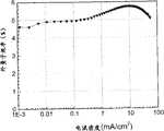
图11显示了图10的器件的电流密度对电压的图。FIG. 11 shows a plot of current density versus voltage for the device of FIG. 10 .
图12显示了图10的器件的外量子效率(EQE)对电流密度的图。FIG. 12 shows a plot of external quantum efficiency (EQE) versus current density for the device of FIG. 10 .
图13显示了图10的器件的归一化强度(任意单位)对时间的图。FIG. 13 shows a plot of normalized intensity (in arbitrary units) versus time for the device of FIG. 10 .
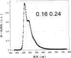
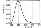
图14显示了图10的器件的归一化场致发光强度对波长的图。FIG. 14 shows a plot of normalized electroluminescence intensity versus wavelength for the device of FIG. 10 .
图15显示了一种已被制造和测试的特定的有机发光器件。Figure 15 shows a specific organic light emitting device that has been fabricated and tested.
图16显示了图15的器件的电流密度对电压的图。FIG. 16 shows a plot of current density versus voltage for the device of FIG. 15 .
图17显示了图15的器件的外量子效率(EQE)对电流密度的图。FIG. 17 shows a plot of external quantum efficiency (EQE) versus current density for the device of FIG. 15 .
图18显示了图15的器件的归一化强度(任意单位)对时间的图。FIG. 18 shows a plot of normalized intensity (in arbitrary units) versus time for the device of FIG. 15 .
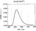
图19显示了图15的器件的归一化场致发光强度对波长的图。FIG. 19 shows a plot of normalized electroluminescence intensity versus wavelength for the device of FIG. 15 .
图20显示了不同器件结构的归一化发光度对时间的图。Figure 20 shows a plot of normalized luminance versus time for different device structures.
图21显示了采用表2中的参数制造的有机发光器件,它具有含不同浓度的磷光材料和非发射材料的第一和第二有机层。Figure 21 shows organic light emitting devices fabricated using the parameters in Table 2, having first and second organic layers with different concentrations of phosphorescent and non-emissive materials.
图22显示了采用表4中的参数制造的有机发光器件,它具有含不同浓度的磷光材料和非发射材料的第一和第二有机层。Figure 22 shows organic light emitting devices fabricated using the parameters in Table 4, having first and second organic layers with different concentrations of phosphorescent and non-emissive materials.
图23显示了采用表4的参数按照图22制造的器件的归一化场致发光强度对波长的图。Figure 23 shows a plot of normalized electroluminescence intensity versus wavelength for devices fabricated according to Figure 22 using the parameters of Table 4.
图24显示了采用表4的参数按照图22制造的器件的发光效率对发光度的图。Figure 24 shows a plot of luminous efficiency versus luminance for devices fabricated according to Figure 22 using the parameters of Table 4.
图25显示了采用表4的参数按照图22制造的器件的外量子效率对发光度的图。Figure 25 shows a plot of external quantum efficiency versus luminosity for devices fabricated according to Figure 22 using the parameters of Table 4.
图26显示了采用表4的参数按照图22制造的器件的电流密度对电压的图。Figure 26 shows a plot of current density versus voltage for devices fabricated according to Figure 22 using the parameters of Table 4.
图27显示了采用表4的参数按照图22制造的器件的发光度对电压的图。Figure 27 shows a plot of luminance versus voltage for devices fabricated according to Figure 22 using the parameters of Table 4.
图28显示了采用表4的参数按照图22制造的器件的归一化发光度对时间的图。Figure 28 shows a plot of normalized luminance versus time for devices fabricated according to Figure 22 using the parameters of Table 4.
图29显示了采用表6的参数制造的有机发光器件,它具有含不同浓度的磷光材料和非发射材料的第一和第二有机层,一些器件有NPD层,一些则没有NPD层。Figure 29 shows organic light emitting devices fabricated using the parameters of Table 6, having first and second organic layers with varying concentrations of phosphorescent and non-emissive materials, some with and some without NPD layers.
图30显示了没有NPD层的有机发光器件。Figure 30 shows an organic light emitting device without an NPD layer.
图31显示了有NPD层的有机发光器件。Figure 31 shows an organic light emitting device with an NPD layer.
图32显示了图30和图31的器件的外量子效率对发光度的图。FIG. 32 shows a plot of external quantum efficiency versus luminance for the devices of FIGS. 30 and 31 .
图33显示了图30和图31的器件的功效率(power efficacy)对发光度的图。FIG. 33 shows a plot of power efficacy versus luminance for the devices of FIGS. 30 and 31 .
图34显示了图30和图31的器件的发光度对电压的图。FIG. 34 shows a plot of luminance versus voltage for the devices of FIGS. 30 and 31 .
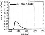
图35显示了图30和图31的器件的场致发光强度对波长的图。FIG. 35 shows a plot of electroluminescence intensity versus wavelength for the devices of FIGS. 30 and 31 .
图36显示了图30的器件在不同的初始发光度下归一化发光度对时间的图。FIG. 36 shows a plot of normalized luminance versus time for the device of FIG. 30 at different initial luminances.
图37显示了图31的器件在不同的初始发光度下归一化发光度对时间的图。FIG. 37 shows a plot of normalized luminance versus time for the device of FIG. 31 at different initial luminances.
图38显示了具有来自NPD和BAlq的发射的有机发光器件。Figure 38 shows an organic light emitting device with emission from NPD and BAlq.
图39显示了图38的器件的外量子效率对发光度的图。FIG. 39 shows a plot of external quantum efficiency versus luminance for the device of FIG. 38 .
图40显示了图38的器件的功效率对发光度的图。FIG. 40 shows a plot of power efficiency versus luminance for the device of FIG. 38 .
图41显示了图38的器件的发光度对电压的图。FIG. 41 shows a plot of luminance versus voltage for the device of FIG. 38 .
图42显示了图38的器件的场致发光强度(任意单位)对波长的图。FIG. 42 shows a plot of electroluminescence intensity (arbitrary units) versus wavelength for the device of FIG. 38. FIG.
图43显示了图38的器件的归一化发光度对时间的图。FIG. 43 shows a plot of normalized luminance versus time for the device of FIG. 38 .
图44显示了具有仅来自Alq的发射的有机发光器件。Figure 44 shows an organic light emitting device with emission from Alq only.
图45显示了图44的器件的外量子效率对发光度的图。FIG. 45 shows a plot of external quantum efficiency versus luminance for the device of FIG. 44 .
图46显示了图44的器件的功效率对发光度的图。FIG. 46 shows a plot of power efficiency versus luminance for the device of FIG. 44 .
图47显示了图44的器件的发光度对电压的图。FIG. 47 shows a plot of luminance versus voltage for the device of FIG. 44 .
图48显示了图44的器件的场致发光强度(任意单位)对波长的图。FIG. 48 shows a plot of electroluminescence intensity (arbitrary units) versus wavelength for the device of FIG. 44. FIG.
图49显示了图44的器件的归一化发光度对时间的图。FIG. 49 shows a plot of normalized luminance versus time for the device of FIG. 44 .
图50显示了一种有机发光器件,它在发射层和阳极之间仅具有有高空穴传导率的层,并且具有与用作发射层中的非发射主体相同的材料的空穴封闭层。Figure 50 shows an organic light emitting device having only a layer with high hole conductivity between the emissive layer and the anode, and a hole blocking layer of the same material as the non-emitting host in the emissive layer.
图51显示了图50的器件的归一化发光度对时间的图。FIG. 51 shows a plot of normalized luminance versus time for the device of FIG. 50 .
图52显示了图50的器件的外量子效率对发光度的图。FIG. 52 shows a plot of external quantum efficiency versus luminance for the device of FIG. 50 .
图53显示了图50的器件的功效率对发光度的图。FIG. 53 shows a plot of power efficiency versus luminance for the device of FIG. 50 .
图54显示了图50的器件的发光度对电压的图。FIG. 54 shows a plot of luminance versus voltage for the device of FIG. 50 .
图55显示了图50的器件的场致发光强度对波长的图。FIG. 55 shows a plot of electroluminescence intensity versus wavelength for the device of FIG. 50. FIG.
图56显示了一种有机发光器件,它在发射层和阳极之间仅具有有高空穴传导率的层,并且具有与用作发射层中的非发射主体相同的材料的空穴封闭层以及具有含不同浓度的磷光材料和非发射材料的第一和第二有机层的发射层,其中第二有机层中磷光材料的浓度是可变的。Fig. 56 shows an organic light-emitting device having only a layer with high hole conductivity between the emissive layer and the anode, and having a hole-blocking layer of the same material as the non-emitting host in the emissive layer and having An emissive layer comprising first and second organic layers of different concentrations of phosphorescent material and non-emissive material, wherein the concentration of phosphorescent material in the second organic layer is variable.
图57显示了图56的器件的归一化发光度对时间的图。FIG. 57 shows a plot of normalized luminance versus time for the device of FIG. 56 .
图58显示了图56的器件的外量子效率对发光度的图。FIG. 58 shows a plot of external quantum efficiency versus luminance for the device of FIG. 56 .
图59显示了图56的器件的功效率对发光度的图。FIG. 59 shows a plot of power efficiency versus luminance for the device of FIG. 56 .
图60显示了图56的器件的发光度对电压的图。FIG. 60 shows a plot of luminance versus voltage for the device of FIG. 56 .
图61显示了图56的器件的场致发光强度对波长的图。FIG. 61 shows a plot of electroluminescence intensity versus wavelength for the device of FIG. 56. FIG.
图62显示了一种有机发光器件,它在发射层和阳极之间仅具有有高空穴传导率的层,并且具有与用作发射层中的非发射主体相同的材料的空穴封闭层以及在第一和第二有机发射层中含有不同磷光材料的具有第一和第二有机层的发射层,其中第二有机层中磷光材料的浓度是可变的。Fig. 62 shows an organic light-emitting device having only a layer with high hole conductivity between the emissive layer and the anode, and a hole-blocking layer of the same material as the non-emitting host in the emissive layer and an An emissive layer having first and second organic layers containing different phosphorescent materials in the first and second organic emissive layers, wherein the concentration of the phosphorescent material in the second organic layer is variable.
图63显示了图62的器件的外量子效率对发光度的图。FIG. 63 shows a plot of external quantum efficiency versus luminance for the device of FIG. 62 .
图64显示了图62的器件的功效率对发光度的图。FIG. 64 shows a plot of power efficiency versus luminance for the device of FIG. 62 .
图65显示了图62的器件的发光度对电压的图。FIG. 65 shows a plot of luminance versus voltage for the device of FIG. 62 .
图66显示了图62的器件的场致发光强度对波长的图。FIG. 66 shows a plot of electroluminescence intensity versus wavelength for the device of FIG. 62. FIG.
发明详述Detailed description of the invention
一般地,OLED包括布置在阳极和阴极之间并且电连接到阳极和阴极上的至少一个有机层。当施加电流时,阳极注入空穴和阴极注入电子到所述有机层中。注入的空穴和电子各自向着带相反电荷的电极迁移。当电子和空穴定域在同一分子上时,形成了“激子”,所述激子是具有激发能态的定域的电子-空穴对。当激子通过光发射机理松驰时,光被发射。在一些情况下,所述激子可以定域在受激准分子或激态复合物上。非辐射机理如热弛豫也可能发生,但一般被认为是不希望的。Generally, an OLED includes at least one organic layer disposed between and electrically connected to an anode and a cathode. When a current is applied, the anode injects holes and the cathode injects electrons into the organic layer. The injected holes and electrons each migrate toward oppositely charged electrodes. When electrons and holes are localized on the same molecule, "excitons," which are localized electron-hole pairs with excited energy states, are formed. Light is emitted when the excitons relax through a photoemission mechanism. In some cases, the excitons can be localized on excimers or exciplexes. Non-radiative mechanisms such as thermal relaxation may also occur, but are generally considered undesirable.
采用从发射分子的单线态发光(“荧光”)的发射分子的初始OLED被公开在例如美国专利4,769,292中,该专利全部内容通过引用结合到本文中。荧光发射通常在小于10毫微秒的时间范围内发生。Primitive OLEDs employing emissive molecules that emit light ("fluorescence") from their singlet state are disclosed, for example, in US Patent 4,769,292, which is incorporated herein by reference in its entirety. Fluorescent emission typically occurs on a time scale of less than 10 nanoseconds.
最近,已经证实了具有从三重态发光(“磷光”)的发射材料的OLED。Baldo等人,“Highly Efficient Phosphorescent Emission fromOrganic Electroluminescent Devices”,Nature(自然),395卷,151-154,1998(“Baldo-I”);和Baldo等人,“Very high-efficiencygreen organic light-emitting devices based onelectrophosphorescence”,Appl.Phys.Lett.(应用物理通讯),75卷,No.3,4-6(1999)(“Baldo-II”),它们的全部内容通过引用结合在本文中。磷光被更详细地描述在美国专利7,279,704的5-6栏中,所述内容通过引用结合在本文中。More recently, OLEDs with emissive materials that emit light from a triplet state ("phosphorescence") have been demonstrated. Baldo et al., "Highly Efficient Phosphorescent Emission from Organic Electroluminescent Devices", Nature, Vol. 395, 151-154, 1998 ("Baldo-I"); and Baldo et al., "Very high-efficiency green organic light-emitting devices based on electrophosphorescence", Appl. Phys. Lett., Vol. 75, No. 3, 4-6 (1999) ("Baldo-II"), the entire contents of which are incorporated herein by reference. Phosphorescence is described in more detail in columns 5-6 of US Patent 7,279,704, which is incorporated herein by reference.
图1显示了有机发光器件100。这些图不一定按比例画出。器件100可包括基材110,阳极115,空穴注入层120,空穴传输层125,电子封闭层130,发射层135,空穴封闭层140,电子传输层145,电子注入层150,保护层155,和阴极160。阴极160是具有第一导电层162和第二导电层164的复合阴极。器件100可以通过按照顺序沉积所述层来制造的。这些不同层的性质和功能以及示例材料被更详细地描述在US 7,279,704的6-10栏中,所述内容通过引用结合在本文中。FIG. 1 shows an organic
对于这些层的每一层来说都有更多实例可以获得。例如,柔性和透明的基材-阳极组合被公开在美国专利5,844,363中,其全部内容通过引用结合在本文中。p-掺杂的空穴传输层的一个实例是按照50∶1的摩尔比用F4-TCNQ掺杂的m-MTDATA,公开于美国专利申请公开号2003/0230980中,其全部内容通过引用结合在本文中。发射材料和主体材料的实例被公开在授予Thompson等人的美国专利6,303,238中,其全部内容通过引用结合在本文中。n-掺杂的电子传输层的一个实例是按照1∶1的摩尔比用Li掺杂的BPhen,公开于美国专利申请公开号2003/0230980中,其全部内容通过引用结合在本文中。美国专利5,703,436和5,707,745(它们的全部内容通过引用结合在本文中)公开了包括复合阴极在内的阴极的实例,所述复合阴极具有金属如Mg:Ag的薄层,在所述金属薄层上具有层叠的透明的、导电的、溅射沉积的ITO层。封闭层的理论和使用更详细地描述在美国专利6,097,147和美国专利申请公开号2003/0230980中,它们的全部内容通过引用结合在本文中。美国专利申请公开号2004/0174116提供了注入层的实例,其全部内容通过引用结合在本文中。保护层的描述可见于美国专利申请公开号2004/0174116中,其全部内容通过引用结合在本文中。For each of these layers more instances are available. For example, flexible and transparent substrate-anode combinations are disclosed in US Patent 5,844,363, the entire contents of which are incorporated herein by reference. An example of a p-doped hole transport layer is m-MTDATA doped withF4 -TCNQ at a molar ratio of 50:1, disclosed in U.S. Patent Application Publication No. 2003/0230980, the entire contents of which are incorporated by reference in the text. Examples of emissive and host materials are disclosed in US Patent 6,303,238 to Thompson et al., the entire contents of which are incorporated herein by reference. An example of an n-doped electron transport layer is BPhen doped with Li in a 1:1 molar ratio, disclosed in US Patent Application Publication No. 2003/0230980, the entire contents of which are incorporated herein by reference. U.S. Patent Nos. 5,703,436 and 5,707,745 (the entire contents of which are incorporated herein by reference) disclose examples of cathodes including composite cathodes having a thin layer of a metal such as Mg:Ag, on which With stacked transparent, conductive, sputter-deposited ITO layers. The theory and use of seal layers is described in more detail in US Patent 6,097,147 and US Patent Application Publication No. 2003/0230980, the entire contents of which are incorporated herein by reference. Examples of injection layers are provided in US Patent Application Publication No. 2004/0174116, the entire contents of which are incorporated herein by reference. A description of protective layers can be found in US Patent Application Publication No. 2004/0174116, the entire contents of which are incorporated herein by reference.
图2显示了颠倒的OLED 200。该器件包括基材210,阴极215,发射层220,空穴传输层225,和阳极230。器件200可以通过按照顺序沉积所述层来制造。因为最常见的OLED构型具有布置在阳极上的阴极,并且器件200具有布置在阳极230下的阴极215,因此器件200可以被称为“颠倒的”OLED。与讨论器件100时所描述的那些材料类似的材料可以被用于器件200的相应层中。图2提供了如何从器件100的结构中省略掉一些层的一个实例。FIG. 2 shows
在图1和2中示出的简单层状结构是作为非限制性例子提供的,并且可以理解,本发明的实施方案可以与各种其它结构相结合使用。所述的特定材料和结构是举例性质的,并且其它材料和结构可以被使用。功能化的OLED可以通过以不同的方式组合所述的各种层来实现,或者某些层可以被完全省略,基于设计、性能和成本因素。没有具体描述的其它层也可以被包括。可以使用除了具体描述的那些材料之外的材料。虽然在这里提供的许多实施例将各种层描述为包括单一一种材料,但是可以理解,可以使用材料的组合,如主体和掺杂剂的混合物,或更一般地混合物。同时,这些层可具有各种亚层。在这里给予各种层的名称并不是意图严格限制的。例如,在器件200中,空穴传输层225传输空穴并将空穴注入到发射层220中,因此可以被描述为空穴传输层或空穴注入层。在一个实施方案中,OLED可以被描述为具有设置在阴极和阳极之间的“有机层”。该有机层可以包括单个层,或者可以进一步包括例如讨论图1和2时所述的不同有机材料的多个层。The simple layered structures shown in Figures 1 and 2 are provided as non-limiting examples, and it is understood that embodiments of the present invention may be used in conjunction with a variety of other structures. The specific materials and structures described are exemplary, and other materials and structures may be used. Functionalized OLEDs can be achieved by combining the various layers described in different ways, or some layers can be omitted entirely, based on design, performance and cost factors. Other layers not specifically described may also be included. Materials other than those specifically described may be used. While many of the examples provided herein describe the various layers as comprising a single material, it is understood that combinations of materials, such as mixtures of hosts and dopants, or more generally mixtures, may be used. Also, these layers may have various sublayers. The names given to the various layers herein are not intended to be strictly limiting. For example, in
没有具体描述的结构和材料也可以使用,例如由聚合物材料组成的OLED(PLED),如公开在美国专利5,247,190(Friend等人)中的PLED,该专利的全部内容通过引用结合在本文中。作为另一个例子,可以使用具有单个有机层的OLED。OLED可以堆叠,例如如在美国专利5,707,745(Forrest等人)中所述,该专利的全部内容通过引用结合在本文中。OLED结构可以背离在图1和2中图示说明的简单层状结构。例如,基材可以包括有角度的反射面以改进外偶联,如在Forrest等人的美国专利6,091,195中所述的台式结构,和/或在Bulovic等人的美国专利5,834,893中描述的坑形结构,所述专利的全部内容通过引用结合在本文中。Structures and materials not specifically described may also be used, such as OLEDs (PLEDs) composed of polymeric materials, such as the PLEDs disclosed in US Pat. No. 5,247,190 (Friend et al.), which is incorporated herein by reference in its entirety. As another example, OLEDs with a single organic layer can be used. OLEDs can be stacked, for example, as described in US Patent 5,707,745 (Forrest et al.), which is incorporated herein by reference in its entirety. OLED structures can depart from the simple layered structures illustrated in FIGS. 1 and 2 . For example, the substrate may include angled reflective surfaces to improve outcoupling, mesa structures as described in U.S. Patent 6,091,195 to Forrest et al., and/or pit structures as described in U.S. Patent 5,834,893 to Bulovic et al. , the entire content of said patent is incorporated herein by reference.
除非另作说明,各种实施方案的这些层中的任何一层可以通过任何合适的方法沉积。对于有机层,优选的方法包括热蒸发,墨喷(如在美国专利6,013,982和6,087,196中所述的,所述专利的全部内容通过引用结合在本文中),有机气相沉积(OVPD)(如在Forrest等人的美国专利6,337,102中所述的,该专利的全部内容通过引用结合在本文中),和通过有机蒸气喷印(OVJP)的沉积(如在美国专利申请序列号10/233,470中所述的,该专利申请的全部内容通过引用结合在本文中)。其它合适的沉积方法包括旋涂和其它溶液型工艺。溶液型工艺优选在氮或惰性气氛中进行。对于其它层,优选的方法包括热蒸发。优选的图案化方法包括通过掩模的沉积,冷焊(如在美国专利6,294,398和6,468,819中描述的方法,所述专利的全部内容通过引用结合在本文中),和与某些沉积方法如墨喷和OVJD联合的图案化。其它方法也可以使用。被沉积的材料可以被改性,以使得它们与具体的沉积方法相容。例如,取代基如支化或未支化的并优选含有至少3个碳的烷基和芳基可以用于小分子中,以提高它们经历溶液加工的能力。可以使用具有20个碳或更多个碳的取代基,而3-20个碳是优选的范围。具有不对称结构的材料可以比具有对称结构的那些材料有更好的溶液加工性,因为不对称材料可以有更低的重结晶倾向。树状分子取代基可用来提高小分子经历溶液加工的能力。Unless otherwise stated, any of these layers of various embodiments may be deposited by any suitable method. For organic layers, preferred methods include thermal evaporation, inkjet (as described in U.S. Pat. et al., U.S. Patent 6,337,102, which is incorporated herein by reference in its entirety), and deposition by organic vapor jet printing (OVJP) (as described in U.S. Patent Application Serial No. 10/233,470 , the entire content of this patent application is incorporated herein by reference). Other suitable deposition methods include spin coating and other solution-based processes. Solution-type processes are preferably performed under nitrogen or an inert atmosphere. For other layers, preferred methods include thermal evaporation. Preferred patterning methods include deposition through a mask, cold welding (as described in U.S. Pat. Joint patterning with OVJD. Other methods can also be used. Deposited materials can be modified to make them compatible with specific deposition methods. For example, substituents such as alkyl and aryl groups, branched or unbranched and preferably containing at least 3 carbons, can be used in small molecules to enhance their ability to undergo solution processing. Substituents having 20 carbons or more may be used, with 3-20 carbons being the preferred range. Materials with asymmetric structures may have better solution processability than those with symmetric structures because asymmetric materials may have a lower tendency to recrystallize. Dendrimer substituents can be used to enhance the ability of small molecules to undergo solution processing.
按照本发明的实施方案制造的器件可以结合到各种各样的消费产品中,包括平板显示器,计算机显示器,电视,广告牌,内部或外部照明和/或发信号的光源,平视显示器(heads up display),全透明显示器,柔性显示器,激光打印机,电话,移动电话,个人数字助理(PDA),膝上型计算机,数字式摄象机,摄像放像机,取景器,微型显示器,车辆,大面积幕墙,戏院或露天运动场屏幕,或标牌。各种控制机构可用来控制按照本发明制造的器件,包括无源矩阵和有源矩阵。许多的器件预计在人感觉舒适的温度范围如18℃到30℃的范围中使用,更优选在室温(20-25℃)使用。Devices fabricated in accordance with embodiments of the present invention can be incorporated into a wide variety of consumer products, including flat panel displays, computer monitors, televisions, billboards, light sources for interior or exterior lighting and/or signaling, heads up displays display), fully transparent display, flexible display, laser printer, telephone, mobile phone, personal digital assistant (PDA), laptop computer, digital camera, camcorder, viewfinder, microdisplay, vehicle, large area curtain wall , theater or stadium screens, or signage. Various control mechanisms can be used to control devices fabricated in accordance with the present invention, including passive matrix and active matrix. Many devices are intended to be used in a temperature range that is comfortable for humans, such as the range of 18°C to 30°C, more preferably at room temperature (20-25°C).
本文描述的材料和结构可以应用在不同于OLED的器件中。例如,其它光电器件如有机太阳能电池和有机光检测器可以使用所述材料和结构。更一般地,有机器件如有机晶体管可以使用所述材料和结构。The materials and structures described herein may find application in devices other than OLEDs. For example, other optoelectronic devices such as organic solar cells and organic photodetectors can use the materials and structures. More generally, organic devices such as organic transistors may use the materials and structures.
术语卤代,卤素,烷基,环烷基,链烯基,炔基,芳烷基,杂环基,芳基,芳族基和杂芳基是本领域已知的,并且被定义在US7,279,704的31-32栏中,所述内容通过引用结合在本文中。The terms halo, halogen, alkyl, cycloalkyl, alkenyl, alkynyl, aralkyl, heterocyclyl, aryl, aromatic and heteroaryl are known in the art and are defined in US7 , 279,704, columns 31-32, the contents of which are incorporated herein by reference.
在本文中使用时,下列化合物具有下列结构:As used herein, the following compounds have the following structures:


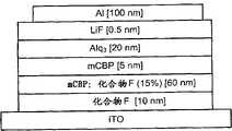
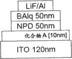
图8显示了一种通用的磷光OLED结构。在某些方面,本发明公开了用于磷光OLED的新结构。图9显示了一种简化的器件结构,它包括在空穴注入层(HIL)和封闭层(BL)之间的一个厚的发射层(EML)。已证实,当磷光OLED中的NPD HTL被化合物B:化合物A掺杂的层代替时,这导致新的绿色磷光OLED的特别长的寿命。已证实具有600

本文公开的一些特征使得磷光OLED稳定性能够显著改善。这包括材料(化合物B)的利用,最初设计该材料是用作主体,但现在已证实它是有效的BL(封闭层)和HTL(空穴传输层)。Some of the features disclosed herein enable significant improvements in phosphorescent OLED stability. This includes the utilization of a material (compound B) which was originally designed to be used as a host but has now been shown to be effective as a BL (blocking layer) and HTL (hole transport layer).
以下文献的全文通过引用结合在本文中:Vadim Adamovich,Novelmaterials and techniques of fabrication for Organic lightemitting diodes(制造有机发光二极管的新材料和技术),PhD,Thesis(博士论文),11.25.2003公布;Peter Mackenzie,VadimAdamovich,Yeh Tung,Michael S.Weaver.EML ON ITO OLED DEVICES,临时申请#60/763,189;美国专利7,022,421;美国专利7,078,113;美国专利公开号2006/0280965。The following documents are hereby incorporated by reference in their entirety: Vadim Adamovich, Novel materials and techniques of fabrication for Organic light emitting diodes (New materials and techniques for the manufacture of organic light emitting diodes), PhD, Thesis (PhD dissertation), published 11.25.2003; Peter Mackenzie , Vadim Adamovich, Yeh Tung, Michael S. Weaver. EML ON ITO OLED DEVICES,
CBP主体、HPT封闭层(BL)和NPD空穴传输层(HTL)材料的低稳定性是实现稳定和长寿命的绿色磷光OLED的重大障碍。更稳定的材料如化合物B在绿色磷光OLED中在发射层、BL和HTL中的使用允许绿色磷光OLED的寿命改善约10倍。对于绿色器件来说,用化合物A掺杂的化合物B的层代替NPD HTL大大改善器件寿命。该概念也适用于蓝色器件。The low stability of the CBP host, HPT blocking layer (BL), and NPD hole transport layer (HTL) materials is a significant obstacle to realize stable and long-lived green phosphorescent OLEDs. The use of more stable materials such as Compound B in the emissive layer, BL and HTL in green phosphorescent OLEDs allows about a 10-fold improvement in the lifetime of green phosphorescent OLEDs. For green devices, replacing the NPD HTL with a layer of compound A doped with compound B greatly improves the device lifetime. This concept also applies to blue devices.
化合物B是非常稳定的主体材料。本发明公开了具有化合物B的绿色结构和性能,该化合物B作为主体、封闭层和空穴传输层的组分用在器件内的各层中。表1显示了有关改善绿色磷光OLED稳定性的器件数据。图8显示了一种通用的器件结构,其显示了表1的各层的结构。Compound B is a very stable host material. The present invention discloses a green structure and properties with compound B, which is used in each layer in the device as a component of host, sealing layer and hole transport layer. Table 1 shows device data on improved stability of green phosphorescent OLEDs. Figure 8 shows a generic device structure showing the structure of the layers of Table 1.
表1:由于器件结构中的新材料导致的绿色磷光OLED性能的进展Table 1: Progress in green phosphorescent OLED performance due to new materials in the device structure

*由加速的LT预测的* predicted by accelerated LT
如从表1可以看出的,将化合物B稳定材料作为各种层引入所述器件显著改善了该器件的寿命。尽管不想受理论的限制,但HTL替代改善了所述器件。据信这对于绿色器件来说可能是尤其重要的。NPD在绿色器件中不如在其它器件如红色器件中稳定。再次地,不想受理论的限制,但据信NPD可以被漏过发射层的电子和(或)被磷光激子劣化。如表1中所示,更稳定的化合物B:化合物A层代替NPD HTL将器件寿命提高至四倍。在包括化合物A和化合物B二者的层内,化合物B传输电子,而化合物A掺杂剂传输空穴。替代NPD使绿色器件的寿命与红色器件的寿命类似(>100,000h)。掺杂的HTL的相同概念可以利用其它材料来使用,并且可以被应用于红色和蓝色磷光OLEDs。As can be seen from Table 1, the introduction of Compound B stabilizing materials as various layers into the device significantly improved the lifetime of the device. While not wanting to be bound by theory, HTL substitution improves the device. It is believed that this may be especially important for green devices. NPD is not as stable in green devices as in other devices such as red devices. Again, without wishing to be bound by theory, it is believed that the NPD may be degraded by electrons leaking through the emissive layer and/or by phosphorescent excitons. As shown in Table 1, replacing the NPD HTL with the more stable Compound B:Compound A layer increased the device lifetime by a factor of four. In a layer that includes both Compound A and Compound B, Compound B transports electrons while the Compound A dopant transports holes. Substituting NPD made the lifetime of the green device similar to that of the red device (>100,000h). The same concept of doped HTL can be used with other materials and can be applied to red and blue phosphorescent OLEDs.
可以考虑的其它器件结构包括梯度结构(graded structure),其中HIL是100%的p-型掺杂剂如化合物A,然后引入主体材料如化合物B作为远离阳极的材料。在阳极和BL或ETL之间也可以采用不同浓度(0-100%)的掺杂剂和主体的多个层。Other device structures that may be considered include graded structures, where the HIL is 100% p-type dopant such as compound A, and then a host material such as compound B is introduced as the material away from the anode. Multiple layers of different concentrations (0-100%) of dopants and hosts between the anode and the BL or ETL can also be employed.
化合物B也可以用作红色和蓝-绿色发射体的主体。Compound B can also be used as host for red and blue-green emitters.
化合物B也可以用作红绿色、蓝色或白色或任何其它颜色的器件中的BL。Compound B can also be used as BL in devices of red green, blue or white or any other color.
具有600
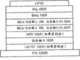
具有化合物B:化合物A掺杂的HTL的特定器件实例归纳于表2中。图21提供了表2中所述器件的结构。Specific device examples with Compound B:Compound A doped HTL are summarized in Table 2. Figure 21 provides the structure of the devices described in Table 2.
表2:当器件中的NDP HTL被替代时器件性能比较Table 2: Device performance comparison when NDP HTL is replaced in the device

*由加速的LT预测的* predicted by accelerated LT
用稳定的掺杂的HTL(化合物B:化合物A)替代NPD导致绿色器件寿命的显著提高。试验结果示于表1和2和相关附图中。具有600

在表2中显示的特定试验中测得的器件的优越性能和最佳性能(其是长寿命与高器件效率和低操作电压的组合)是表2中的实施例5。图9中显示了实施例5的结构。这个器件仅有三种有机材料。该器件的HIL、EML和BL可以被认为是具有从邻接ITO(空穴注入界面)的100%化合物A至邻接Alq ETL(电子注入界面)的100%化合物B的梯度浓度的化合物A:化合物B层。The superior and best performance of the device (which is the combination of long lifetime with high device efficiency and low operating voltage) measured in the specific tests shown in Table 2 is Example 5 in Table 2. The structure of
表1和2的器件说明了与优越的器件性能相关的以下几点。The devices of Tables 1 and 2 illustrate the following points associated with superior device performance.
○掺杂的HTL(稳定的基质(不必是空穴传输性的)和空穴传输掺杂剂)(也可能ETL)的利用○ Utilization of doped HTL (stable host (not necessarily hole-transporting) and hole-transporting dopant) (also ETL)
○相同材料(主体和掺杂剂)用于HTL和发射层的利用○ Utilization of the same material (host and dopant) for HTL and emitter layer
○相同材料(例如化合物A)作为绿色磷光发射掺杂剂和空穴传输掺杂剂和空穴注入层的利用○ Utilization of the same material (e.g. Compound A) as green phosphorescent emitting dopant and hole transport dopant and hole injection layer
○相同材料(例如化合物B)作为EML中的主体、HTL中的基质、器件中的封闭层(纯的)的利用○ Utilization of the same material (e.g. compound B) as host in EML, matrix in HTL, sealing layer (pure) in devices
○器件中仅有三种材料(例如化合物A、化合物B、Alq)○ Only three materials in the device (e.g. Compound A, Compound B, Alq)
○高稳定性的绿色磷光结构(在1000尼特下超过300,000小时的寿命)○ High stability green phosphorescent structure (over 300,000 hours lifespan at 1000 nits)
另外,公开了具有以下优选结构的器件结构,它们可单独或组合使用:In addition, device structures with the following preferred structures are disclosed, which can be used alone or in combination:
稳定的主体,如苯并[9,10]菲化合物,例如化合物B的利用Stable hosts such as benzo[9,10]phenanthrene compounds, such as the utilization of compound B
1.作为PHOLEDs的主体的苯并[9,10]菲化合物1. Benzo[9,10]phenanthrene compounds as hosts of PHOLEDs
2.作为PHOLEDs中的封闭或阻抗层的苯并[9,10]菲化合物2. Benzo[9,10]phenanthrene compounds as blocking or resistive layers in PHOLEDs
3.作为同一OLED中的主体和封闭层的苯并[9,10]菲化合物3. Benzo[9,10]phenanthrene compounds as host and capping layer in the same OLED
4.作为同一OLED中的主体和HTL组分的苯并[9,10]菲化合物4. Benzo[9,10]phenanthrene compounds as host and HTL components in the same OLED
5.作为同一OLED中的HTL的组分和封闭层的苯并[9,10]菲化合物5. Benzo[9,10]phenanthrene compounds as components and sealing layers of HTL in the same OLED
6.作为同一器件如三组分器件中的HTL的组分、主体和封闭层的苯并[9,10]菲化合物6. Benzo[9,10]phenanthrene compounds as components, hosts, and capping layers of HTL in the same device, such as a three-component device
7.有或没有电子传输层的结构1-6。7. Structures 1-6 with or without electron transport layer.
8.使用化合物B作为具体的苯并[9,10]菲化合物的结构1-7。8. Structures 1-7 using Compound B as the specific benzo[9,10]phenanthrene compound.
9.上述结构1-7,但使用咔唑化合物代替苯并[9,10]菲化合物作为稳定的主体。9. Structures 1-7 above, but using a carbazole compound instead of a benzo[9,10]phenanthrene compound as a stable host.
10.使用mCBP或化合物R作为具体的咔唑化合物的结构9。10.
器件可以使用稳定的主体材料即苯并[9,10]菲化合物或咔唑化合物制造。所述器件可以包括仅3种或仅2种有机组分,并且可以包括具有不同浓度的相同材料的多个层。表3显示了这样的器件的实例。图8中显示了表3的器件的结构。图8中关于HTL和ETL的命名在一定程度上是可变通的,因为据信这两层在许多结构,特别是其中HTL和ETL具有相同材料但浓度不同的那些结构中都发射。表3的器件1和2实际上已被制造,而器件3和4没有被制造,但为了说明的目的将器件3和4包括在表3中。据信化合物S是可以在发射层中传输电子的磷光分子的一个实例。Devices can be fabricated using stable host materials, namely benzo[9,10]phenanthrene compounds or carbazole compounds. The device may comprise only 3 or only 2 organic components and may comprise multiple layers with different concentrations of the same material. Table 3 shows examples of such devices. The structure of the devices of Table 3 is shown in FIG. 8 . The nomenclature in Figure 8 with respect to HTL and ETL is somewhat flexible, as it is believed that both layers emit in many structures, particularly those in which HTL and ETL have the same material but in different concentrations.
表3:基于在不同层内的不同浓度的相同材料的“3组分”和“2组分”磷光OLED结构的实例Table 3: Examples of "3-component" and "2-component" phosphorescent OLED structures based on different concentrations of the same material in different layers

所述器件可以应用在平板显示器和照明中。所述已证实的优越的器件具有能在高效磷光OLEDs中实现更长寿命的优点。无需专门的制造设备,而且可以通过本领域已知的方法制造器件。可以考虑荫罩,取决于常见的层是否能用在并列RGB应用的情况中。The devices can be used in flat panel displays and lighting. The proven superior devices have the advantage of enabling longer lifetimes in high-efficiency phosphorescent OLEDs. No specialized fabrication equipment is required, and devices can be fabricated by methods known in the art. Shadow masks may be considered, depending on whether common layers can be used in the case of side-by-side RGB applications.
图3显示了一种有机发光器件,它具有含不同浓度的磷光材料和非发射材料的第一和第二有机层,以及在第一有机层和阳极之间的具有特殊载流子迁移率特性的有机层。如所图示的,图3的器件包括基材310、阳极315、第三有机层320、具有第一有机层330和第二有机层340的发射层、空穴封闭层350、电子传输层360和阴极370。空穴封闭层350和电子传输层360是任选的。图3的器件和本文中显示的各种其它器件被显示为具有与基材邻接的阳极,如许多器件中常见的那样,但所述器件也可以具有与基材邻接的阴极。Figure 3 shows an organic light-emitting device with first and second organic layers containing different concentrations of phosphorescent and non-emissive materials, and special carrier mobility characteristics between the first organic layer and the anode of the organic layer. As illustrated, the device of FIG. 3 includes a substrate 310, an anode 315, a third organic layer 320, an emissive layer having a first organic layer 330 and a second organic layer 340, a
第一有机层330布置在阴极和阳极之间,并且包括磷光材料和非发射材料。第一有机层中磷光材料的浓度为10-90wt%。第一有机层中非发射材料的浓度为10-90wt%。第二有机层340布置在第一有机层和阴极之间。第二有机层340优选直接与第一有机层330接触,但是在第一和第二有机层330和340之间也可以有能传输电子和空穴的薄的有机层。第二有机层也包括磷光材料和非发射材料。所述第二层内磷光材料的浓度为3-25wt%。第二有机层中非发射材料的浓度为75-97wt%。第二有机层中磷光材料的浓度比第一有机层中磷光材料的浓度低。由于第一和第二有机层330和340中磷光材料的不同浓度,在这些层间存在界面。在一个方面,第一和第二有机层330和340仅包括磷光材料和非发射材料。这是有利的,因为将材料的数目最小化简化了制造,并且避免了可能与另外的材料相关的故障机理。The first organic layer 330 is disposed between the cathode and the anode, and includes a phosphorescent material and a non-emissive material. The concentration of the phosphorescent material in the first organic layer is 10-90 wt%. The concentration of the non-emissive material in the first organic layer is 10-90 wt%. The second organic layer 340 is disposed between the first organic layer and the cathode. The second organic layer 340 is preferably in direct contact with the first organic layer 330, but there may also be a thin organic layer between the first and second organic layers 330 and 340 capable of transporting electrons and holes. The second organic layer also includes phosphorescent material and non-emissive material. The concentration of the phosphorescent material in the second layer is 3-25wt%. The concentration of non-emissive material in the second organic layer is 75-97 wt%. The concentration of the phosphorescent material in the second organic layer is lower than the concentration of the phosphorescent material in the first organic layer. Due to the different concentrations of phosphorescent materials in the first and second organic layers 330 and 340, an interface exists between these layers. In one aspect, the first and second organic layers 330 and 340 include only phosphorescent and non-emissive materials. This is advantageous because minimizing the number of materials simplifies manufacturing and avoids failure mechanisms that may be associated with additional materials.
图3和其它附图显示了包括“磷光”材料和“非发射”材料的有机层。Figure 3 and other figures show organic layers comprising "phosphorescent" materials and "non-emissive" materials.
在本文中使用的“磷光”材料是能够在室温,例如在约18-25摄氏度下从三重激发态发射光的材料。然而,任何给定的磷光材料在特定的层或在特定的器件中可以发光或不发光。在本文中公开的许多结构中,所述磷光材料发射光。然而,在其它结构中,磷光材料不发射光,而是向可以是磷光性或荧光性的其它分子传输激子,然后所述其它分子发射光。在这些器件中材料的磷光性质仍然发挥作用,因为在室温下从三重激发态发光的能力与其它性质如系间窜跃(intersystemcrossing)和强自旋轨道耦合有关,所述其它性质允许三重态在分子上有效形成并传输给其它分子,尽管它可能不发射光。另外,许多磷光材料也是好的空穴传输体。本申请中定义的术语“磷光”的定义据信大体上与其在本领域中的使用一致,但是不想推广到该术语可能以不同的方式使用的其它用途。As used herein, a "phosphorescent" material is a material capable of emitting light from a triplet excited state at room temperature, for example at about 18-25 degrees Celsius. However, any given phosphorescent material may or may not emit light in a particular layer or in a particular device. In many of the structures disclosed herein, the phosphorescent material emits light. In other structures, however, the phosphorescent material does not emit light, but rather transfers excitons to other molecules, which may be phosphorescent or fluorescent, which then emit light. The phosphorescent properties of the material still play a role in these devices because the ability to emit light from triplet excited states at room temperature is related to other properties such as intersystem crossing and strong spin-orbit coupling that allow triplet states to Efficiently formed on a molecule and transmitted to other molecules, although it may not emit light. In addition, many phosphorescent materials are also good hole transporters. The definition of the term "phosphorescence" as defined in this application is believed to be generally consistent with its use in the art, but is not intended to extend to other uses where the term may be used differently.
在本文中使用的“非发射”材料在所述器件中不发射光,因此该材料被描述为“非发射的”。然而,非发射材料在所述器件中不必然是电惰性的,并且可能经常涉及电荷传输,最经常涉及电子传输。该材料在其它情况中可能是发射性的,例如在溶液中或在其它器件中。通常,如果“非发射”材料在除了它作为非发射材料被包括在其中的器件外的情况中能够发射光,则在该特定器件中固体状态方面的原因导致该材料在所述器件中不发射光。例如,“非发射”材料可以用三重态能量比非发射材料的三重态能量低至少0.1eV的磷光材料掺杂,使得在所述非发射材料上形成的任何三重态转移到所述磷光材料而不是发射光。As used herein, a "non-emissive" material does not emit light in the device, and thus the material is described as "non-emissive." However, non-emissive materials are not necessarily electrically inert in the device and may often be involved in charge transport, most often electron transport. The material may be emissive in other situations, such as in solution or in other devices. In general, if a "non-emissive" material is capable of emitting light in conditions other than the device in which it is included as a non-emissive material, there is a reason in the solid state in that particular device that the material does not emit in said device Light. For example, a "non-emitting" material may be doped with a phosphorescent material having a triplet energy at least 0.1 eV lower than that of the non-emitting material, such that any triplet formed on the non-emitting material is transferred to the phosphorescent material instead of Not emitting light.
关于本发明的各方面如何发挥作用不受任何理论限制,据信,在许多磷光OLED中,重组发生在器件中某处的界面或界面附近,因为在界面的任何一侧电子和空穴迁移率可能是不同的,并且因为电子和空穴穿过界面可能有困难。如果发射层不包括任何内界面,重组可能发生在发射层与非发射层的界面或界面附近。因此,激子和两种类型的载流子以显著的浓度定位于所述非发射层附近。如果非发射层易受来自激子和/或载流子的损伤,器件寿命可能被不利地影响。另外,非发射层与重组区接近可以为激子提供非发射衰变路线,这不利地影响器件效率。Without being bound by any theory as to how aspects of the invention work, it is believed that, in many phosphorescent OLEDs, recombination occurs at or near the interface somewhere in the device because electron and hole mobility on either side of the interface may be different, and because electrons and holes may have difficulty crossing the interface. If the emissive layer does not include any internal interfaces, recombination may occur at or near the interface of the emissive layer with the non-emissive layer. Thus, excitons and both types of carriers are localized in significant concentrations near the non-emissive layer. If the non-emitting layer is susceptible to damage from excitons and/or carriers, device lifetime may be adversely affected. Additionally, the proximity of the non-emissive layer to the recombination region can provide non-emissive decay routes for excitons, which adversely affects device efficiency.
还据信,在许多磷光器件中磷光材料负责在发射层中空穴的传输,并且非发射主体材料负责电子的传输。据信,第一有机层330和第二有机层340之间磷光材料浓度的变化可引起第一有机层330中电子的迁移率比第二有机层340中电子的迁移率高,并且第二有机层340中空穴的迁移率比第一有机层330中空穴的迁移率高。结果,电子和空穴的重组可以发生在第一有机层330和第二有机层340之间的界面或界面附近。第二有机层340中磷光材料的浓度优选比第一有机层330中的浓度低至少5wt%,更优选低至少10wt%。第一有机层330和第二有机层340一起可以形成所述器件的发射层。因为重组发生在第一和第二有机层330和340之间的界面或界面附近,即在发射层内的界面处,所以可以避免在与非发射层的界面附近由重组引起的问题。这些段落中描述的推理适用于本文中描述的各种器件,所述器件具有有内界面,即在第一和第二有机层之间的界面的发射层。It is also believed that in many phosphorescent devices the phosphorescent material is responsible for the transport of holes in the emissive layer and the non-emitting host material is responsible for the transport of electrons. It is believed that the change in the concentration of the phosphorescent material between the first organic layer 330 and the second organic layer 340 can cause the mobility of electrons in the first organic layer 330 to be higher than the mobility of electrons in the second organic layer 340, and that the second organic layer The mobility of holes in layer 340 is higher than the mobility of holes in first organic layer 330 . As a result, recombination of electrons and holes may occur at or near the interface between the first organic layer 330 and the second organic layer 340 . The concentration of the phosphorescent material in the second organic layer 340 is preferably at least 5 wt % lower than that in the first organic layer 330 , more preferably at least 10 wt %. Together, the first organic layer 330 and the second organic layer 340 may form an emission layer of the device. Since recombination occurs at or near the interface between the first and second organic layers 330 and 340, ie, at the interface within the emissive layer, problems caused by recombination near the interface with the non-emissive layer can be avoided. The reasoning described in these paragraphs applies to the various devices described herein having an emissive layer with an internal interface, ie, the interface between the first and second organic layers.
第一有机层330和第二有机层340的磷光材料可以是相同的材料,或者可以是不同的磷光材料。第一有机层330和第二有机层340的非发射材料可以是相同的材料或不同的材料。因此,存在四种组合:(1)第一和第二两个有机层内的磷光材料相同,而且第一和第二两个有机层内的非发射材料相同;(2)第一和第二有机层中的磷光材料不同,而第一和第二两个有机层内的非发射材料相同;(3)第一和第二两个有机层内的磷光材料相同,而且第一和第二有机层中的非发射材料不同;和(4)第一和第二有机层中的磷光材料不同,而且第一和第二有机层中的非发射材料不同。每种组合都有优点。The phosphorescent materials of the first organic layer 330 and the second organic layer 340 may be the same material, or may be different phosphorescent materials. The non-emissive materials of the first organic layer 330 and the second organic layer 340 may be the same material or different materials. Therefore, there are four combinations: (1) the phosphorescent material in the first and second two organic layers is the same, and the non-emissive material in the first and second two organic layers is the same; (2) the first and second The phosphorescent materials in the organic layer are different, and the non-emitting materials in the first and second two organic layers are the same; (3) the phosphorescent materials in the first and second two organic layers are the same, and the first and second organic layers The non-emissive materials in the layers are different; and (4) the phosphorescent materials in the first and second organic layers are different, and the non-emissive materials in the first and second organic layers are different. Each combination has advantages.
在第一有机层330和第二有机层340中使用相同的非发射材料通过减少该器件中材料的数目而简化了制造。另外,由于每种新材料可能引入新的故障机制,因此在多个层内使用相同的材料可以减少故障机制。使用相同的非发射材料也可以有助于扩大所述器件的重组区域,这也有助于实现更高的器件寿命,同时通过调整界面处非发射材料的浓度仍允许重组在第一有机层330和第二有机层340之间的界面附近发生。Using the same non-emissive material in the first organic layer 330 and the second organic layer 340 simplifies fabrication by reducing the number of materials in the device. Additionally, using the same material within multiple layers reduces failure mechanisms since each new material may introduce new failure mechanisms. Using the same non-emitting material can also help to expand the recombination area of the device, which also helps to achieve higher device lifetime, while still allowing recombination in the first organic layer 330 and Occurs near the interface between the second organic layers 340 .
然而,在第一有机层330和第二有机层340中使用不同的非发射材料也有优点。不同的材料可以具有不同的电荷传输性质。如果非发射材料主要负责特定载流子(最经常是电子)的传输,在第一有机层330和第二有机层340中使用不同的非发射材料可以使得控制在器件中发生重组的位置更容易。具体地说,通过为第一有机层330和第二有机层340选择不同的非发射材料,在第一有机层330和第二有机层340之间的界面附近产生载流子梯度可以更容易,因为除了非发射材料的浓度之外,非发射材料的不同也可以用于实现此目的。However, there are also advantages to using different non-emissive materials in the first organic layer 330 and the second organic layer 340 . Different materials can have different charge transport properties. Using different non-emissive materials in the first organic layer 330 and the second organic layer 340 can make it easier to control where recombination occurs in the device if the non-emissive material is primarily responsible for the transport of specific carriers (most often electrons). . Specifically, by selecting different non-emissive materials for the first organic layer 330 and the second organic layer 340, it may be easier to generate a carrier gradient near the interface between the first organic layer 330 and the second organic layer 340, Because in addition to the concentration of the non-emitting material, the difference of the non-emitting material can also be used for this purpose.
在第一有机层330和第二有机层340中以不同浓度使用相同的磷光材料,具有许多上面关于使用相同的非发射材料所描述的同样的优点。材料种类越少可能意味着故障机制越少。不同的浓度可以允许重组被控制在第一有机层330和第二有机层340之间的界面附近发生,而使用相同的磷光材料允许重组区域相对宽。Using the same phosphorescent material at different concentrations in the first organic layer 330 and the second organic layer 340 has many of the same advantages described above with respect to using the same non-emissive material. Fewer material types can mean fewer failure mechanisms. Different concentrations may allow recombination to be controlled to occur near the interface between the first organic layer 330 and the second organic layer 340, while using the same phosphorescent material allows the recombination region to be relatively wide.
在第一有机层330和第二有机层340中以不同的浓度使用不同的磷光材料,具有许多上面关于使用不同的非发射材料所描述的同样的优点。不同材料的使用可以增加可用来控制重组发生位置的额外的参数。Using different phosphorescent materials at different concentrations in the first organic layer 330 and the second organic layer 340 has many of the same advantages described above with respect to using different non-emissive materials. The use of different materials can add additional parameters that can be used to control where recombination occurs.
另外,磷光材料在器件中可以发射或不发射光。在希望高效的饱和发射(可能用于要求饱和发射的显示器)的情况下,在第一有机层330和第二有机层340中使用相同的磷光材料作为发射材料可能是优选的。在其中磷光材料传输电荷但不发光的构型中,被称作“低能量”材料的另外的材料可以被加到第一有机层330和第二有机层340中并发射光。所谓“低能量”是指该低能量发射材料的发射光谱的峰比同一层内的磷光材料的发射光谱的峰高至少20nm。较高的波长对应于较低的能量。激子可以通过许多机理存在在所述低能量发射材料上,并且不意图限制激子到达所述低能量发射材料的方式。例如,激子可以在所述磷光材料上形成并转移到所述低能量发射材料,或者激子可以直接在所述低能量发射材料上形成。在一种构型中,所述低能量发射材料可以是接受来自磷光材料的激子,包括在磷光材料上作为三重态形成的激子的荧光材料。Additionally, phosphorescent materials may or may not emit light in the device. Where efficient saturated emission is desired (possibly for displays requiring saturated emission), it may be preferable to use the same phosphorescent material in the first organic layer 330 and the second organic layer 340 as the emissive material. In configurations where the phosphorescent material transports charge but does not emit light, additional materials, referred to as "low energy" materials, may be added to the first organic layer 330 and the second organic layer 340 and emit light. The so-called "low energy" means that the peak of the emission spectrum of the low energy emitting material is at least 20nm higher than the peak of the emission spectrum of the phosphorescent material in the same layer. Higher wavelengths correspond to lower energies. Excitons can be present on the low energy emissive material by a number of mechanisms, and it is not intended to limit the manner in which excitons can reach the low energy emissive material. For example, excitons can be formed on the phosphorescent material and transferred to the low energy emissive material, or excitons can be formed directly on the low energy emissive material. In one configuration, the low energy emissive material may be a fluorescent material that accepts excitons from a phosphorescent material, including excitons formed as triplets on the phosphorescent material.
然而,在希望较不饱和的发射(可能是用于一般照明目的的白光)的情况下,在同一个器件中有多分子发射可能是希望的。为此,可将不同的磷光材料用在第一和第二有机层330和340中作为那些层中的发射体,这样在所述器件中有多种发射材料。也可以将被称作“低能量”材料的另外一种或多种材料加到第一和第二有机层330和340之一或两者内。如果希望从多种材料发射,可以将不同的低能量发射材料用在第一和第二有机层330和340两者内,或者可以将低能量发射材料用在第一和第二有机层330和340之一内,而磷光材料从第一和第二有机层330和340中的另一层发射。However, where less saturated emission is desired (perhaps white light for general lighting purposes), multimolecular emission in the same device may be desirable. To this end, different phosphorescent materials can be used in the first and second organic layers 330 and 340 as emitters in those layers, so that there are multiple emitting materials in the device. Another material or materials, referred to as "low energy" materials, may also be added to one or both of the first and second organic layers 330 and 340 . If it is desired to emit from multiple materials, different low-energy emissive materials can be used in both the first and second organic layers 330 and 340, or low-energy emissive materials can be used in the first and second organic layers 330 and 340. 340, while the phosphorescent material is emitted from the other of the first and second organic layers 330 and 340.
然而,具有含第一和第二有机层的发射层的、在第一和第二有机层之间有界面的器件仍可能经历短的寿命。据信,在许多磷光有机发光器件中最主要的故障机制涉及电子从阴极穿过发射层到达发射层的阳极侧的有机层。据信,用在OLEDs的阳极侧的许多有机材料易受来自这些电子的损伤。附图44-50和相关内容显示了常见空穴传输材料NPD在缩短器件寿命中的作用。具有第一和第二有机层330和340的发射层的使用有利地允许重组在发射层内的界面处发生。结果,到达非发射层的激子的数目和穿过整个发射层到达另一侧的载流子(即到达发射层的阳极侧的电子和到达发射层的阴极侧的空穴)的数目可以被减少。然而,有利的是具有展开的重组区(这可以通过本文所述的器件结构实现),这样激子和/或载流子可以到达和损伤非发射层,不利地影响器件寿命。据信一种常见的故障机制涉及电子穿过发射层到达发射层的阳极侧,并损伤相邻的非发射层。However, devices having an emissive layer comprising first and second organic layers with an interface between the first and second organic layers may still experience short lifetimes. It is believed that the most dominant failure mechanism in many phosphorescent organic light emitting devices involves electrons passing from the cathode through the emissive layer to the organic layer on the anode side of the emissive layer. It is believed that many of the organic materials used on the anode side of OLEDs are susceptible to damage from these electrons. Figures 44-50 and related texts show the role of common hole transport material NPD in reducing device lifetime. The use of an emissive layer with first and second organic layers 330 and 340 advantageously allows recombination to occur at the interface within the emissive layer. As a result, the number of excitons reaching the non-emissive layer and the number of carriers passing through the emissive layer to the other side (i.e. electrons reaching the anode side of the emissive layer and holes reaching the cathode side of the emissive layer) can be determined by reduce. However, it is advantageous to have an expanded recombination region (which can be achieved with the device structures described herein) so that excitons and/or carriers can reach and damage the non-emitting layers, adversely affecting device lifetime. One common failure mechanism is believed to involve electrons passing through the emissive layer to the anode side of the emissive layer and damaging the adjacent non-emitting layer.
避免由电子损伤发射层阳极侧的有机材料引起的损伤和较短的器件寿命的一种方法,是在发射层的阳极侧仅使用空穴迁移率大大高于电子迁移率的材料。该差别应该足够大,使得在该层中大部分的载流子同属一种类型。参考图3,第三有机层320位于发射层,即第一和/或第二有机层330和340的阳极侧。在被第三有机层320占据的位置可以有多于一层的有机层。在发射层和阳极之间的每一有机层可以包括一种有机材料或多种有机材料。对于单种材料的多层来说,这意味着每层的材料的空穴迁移率大大高于该层的电子迁移率。对于包括多种材料的层来说,这意味着该层的空穴迁移率大大高于该层的电子迁移率。某“层”的空穴迁移率与该层内主要负责在该层内传输空穴的材料的空穴迁移率密切相关,尤其当所述材料以显著的量存在时。电子和空穴迁移率可以通过多种方法测量,包括飞行时间、暗电流注入和导纳谱法。所谓“大大高于”是指空穴迁移率是电子迁移率的至少两倍,优选是电子迁移率的至少十倍,最优选是电子迁移率的至少100倍。One way to avoid damage and shorter device lifetimes caused by electron damage to the organic material on the anode side of the emissive layer is to use only materials on the anode side of the emissive layer with a much higher hole mobility than the electron mobility. The difference should be large enough that most of the carriers in the layer are of the same type. Referring to FIG. 3 , the third organic layer 320 is located on the anode side of the emission layer, ie, the first and/or second organic layers 330 and 340 . There may be more than one organic layer at the position occupied by the third organic layer 320 . Each organic layer between the emissive layer and the anode may include an organic material or organic materials. For multiple layers of a single material, this means that the hole mobility of the material of each layer is much higher than the electron mobility of that layer. For a layer comprising multiple materials, this means that the hole mobility of the layer is substantially higher than the electron mobility of the layer. The hole mobility of a "layer" is closely related to the hole mobility of the material within that layer that is primarily responsible for transporting holes within that layer, especially when said material is present in significant amounts. Electron and hole mobility can be measured by a variety of methods, including time-of-flight, dark current injection, and admittance spectroscopy. By "significantly higher" it is meant that the hole mobility is at least twice the electron mobility, preferably at least ten times the electron mobility, and most preferably at least 100 times the electron mobility.
传统上NPD用作空穴传输层(HTL),并且其经常与EML接触。然而,So等人报道NPD具有类似于它的空穴迁移率(~5x10⁻⁴cm2V-1s-1)的电子迁移率。见So等人,‘在用于OLED的有机小分子中的双极载流子传输’,Proceedings of the Society for Information Display,38,1497(2007)。这表明在常规结构中电子可以容易地被NPD传输。这使得两种可能的不希望的情况发生。首先,电子和空穴可以在NPD中重组。NPD可以是稳定的空穴传输层,但是预期表现出NPD发射的器件不是操作上稳定的,因为所述发射是低效的,并且因此器件不包括NPD。例如,图38中显示了具有NPD和BAlq发射的器件。当器件以20mA/cm2的恒定电流驱动时,图43中显示的该器件的寿命(LT50)小于300小时。作为比较,仅具有Alq发射的类似器件(见图44)具有长得多的寿命。以40mA/cm2的连续驱动电流驱动300小时后,所述Alq发射器件的发光度降到其初始值的约86%(见图49)。其次,NPD可能固有地对电子不稳定。有充分的证据使得可以相信,NPD在仅有空穴的器件中是稳定的;然而,没有证实它对电子的稳定性。NPD is traditionally used as a hole transport layer (HTL), and it is often in contact with the EML. However, So et al. reported that NPD has an electron mobility similar to its hole mobility (˜5×10⁻⁴ cm2 V−1 s−1 ). See So et al., 'Bipolar carrier transport in small organic molecules for OLEDs', Proceedings of the Society for Information Display, 38, 1497 (2007). This suggests that electrons can be easily transported by NPDs in conventional structures. This makes two possible undesired situations happen. First, electrons and holes can recombine in NPDs. NPD can be a stable hole transport layer, but devices exhibiting NPD emission are not expected to be operationally stable because the emission is inefficient, and therefore devices do not include NPD. For example, a device with NPD and BAlq emission is shown in Figure 38. The lifetime (LT50) of the device shown in Figure 43 was less than 300 hours when the device was driven at a constant current of 20 mA/cm2 . In comparison, a similar device with only Alq emission (see Figure 44) has a much longer lifetime. After driving for 300 hours at a continuous driving current of 40 mA/cm2 , the luminance of the Alq emitting device dropped to about 86% of its initial value (see FIG. 49 ). Second, NPD may be inherently unstable to electrons. There is sufficient evidence to believe that NPD is stable in hole-only devices; however, its stability towards electrons has not been demonstrated.
在一个优选的方面,第三有机层320是布置在第一有机层330和阳极315之间的单一有机层,即,第三有机层320与第一有机层330和阳极315直接接触。还在此优选的方面,第三有机层320仅包括第一有机层330的磷光材料。通常,电子存在于器件的发射层内,并且器件的发射材料暴露于在发射层中的电子。结果,在具有相当长寿命的器件中所使用的大部分磷光发射分子耐受来自电子的损伤。因此,以另外的角色使用第一和第二有机层330和340的磷光材料作为在第一有机层330和阳极315之间仅有的有机材料,即作为空穴传输分子,可以导致避免了与电子对发射层阳极侧的有机层损伤相关的故障机制的器件。In a preferred aspect, the third organic layer 320 is a single organic layer disposed between the first organic layer 330 and the anode 315 , ie, the third organic layer 320 is in direct contact with the first organic layer 330 and the anode 315 . Also in this preferred aspect, the third organic layer 320 includes only the phosphorescent material of the first organic layer 330 . Typically, electrons are present within the emissive layer of the device, and the emissive material of the device is exposed to the electrons in the emissive layer. As a result, most phosphorescent emitting molecules used in devices with a relatively long lifetime are resistant to damage from electrons. Therefore, using the phosphorescent material of the first and second organic layers 330 and 340 in an additional role as the only organic material between the first organic layer 330 and the anode 315, i.e. as hole-transporting molecules, can result in avoiding the interaction with Electron damage to the organic layer on the anode side of the emissive layer is associated with the failure mechanism of the device.
避免由电子损伤在发射层阳极侧的有机材料引起的损伤和较短寿命的另一种方法,是在发射层的阳极侧避免使用易受来自电子的损伤的材料种类。据信在发射层的阳极侧通常使用的许多材料易受这样的损害。NPD是这类材料的一个实例。更一般地说,在发射层的阳极侧可以被有利地避免的材料包括具有来自如下名单的基团的分子:三芳基胺,萘基,三(N-咔唑基)三苯胺,四芳基胺和咔唑。Another way to avoid damage and shorter lifetimes caused by electron damage to the organic material on the anode side of the emissive layer is to avoid the use of material species on the anode side of the emissive layer that are susceptible to damage from electrons. It is believed that many materials commonly used on the anode side of the emissive layer are susceptible to such damage. NPD is an example of such a material. More generally, materials that can be advantageously avoided on the anode side of the emissive layer include molecules with groups from the following list: triarylamine, naphthyl, tris(N-carbazolyl)triphenylamine, tetraaryl Amines and carbazoles.
避免由电子损伤在发射层阳极侧的有机材料引起的损伤和较短寿命的另一种方法,是在发射层的阳极侧使用具有高空穴传导率的材料。高空穴传导率可以允许空穴以足以使到达发射层阳极侧的电子的数目减至最少的速率注入发射层。在一个OLED中,某层的电导率的一种实用量度是由制造更厚的特定层在器件中引起的电压升高。具体地说,可以制造除了一个方面的不同-这些器件中电导率正在被测量的特定层在不同的器件中有不同的厚度-外其它方面相同的数个器件。因为所述器件其它方面相同,所以由特定层厚度的增大引起的电压差可以与因各种界面和电导率正在被测量的层之外的各层引起的电压差分离开。具体地说,空穴传导率可以通过在器件中进行这样的测量来测定,在所述器件中不同厚度的所述层位于器件中基于该器件中的其它层电子不能大量到达而空穴在其中是主要的载流子的位置。参数如影响电导率的载流子迁移率可能是电流的函数,尽管据信所述函数关系不强。为了控制这个因素,测量可以在特定的电流密度下进行。10mA/cm2是用于本文所描述的测量的合适的电流密度。已经以该方法测定了NPD的空穴传导率,并且已证实,在10mA/cm2的电流下,NPD的厚度每增加10nm器件两端的电压增大0.6V。以类似的方法测定了LG101TM(可得自韩国的LG)的空穴传导率,并且已证实,在10mA/cm2的电流下,LG101的厚度每增加10nm器件两端的电压增加小于0.5V。这些测量结果在很多种器件结构上是可重复的。在发射层和阳极之间仅具有层厚度每增加10nm器件两端的电压升高0.1V或更小的层的器件,可以有利地将对发射层阳极侧的有机层的损伤减到最小。LG101的层是这样的层的一个实例。Another way to avoid damage and shorter lifetime caused by electrons damaging the organic material on the anode side of the emissive layer is to use a material with high hole conductivity on the anode side of the emissive layer. High hole conductivity can allow holes to be injected into the emissive layer at a rate sufficient to minimize the number of electrons reaching the anode side of the emissive layer. In an OLED, a practical measure of the conductivity of a layer is the voltage rise in the device caused by making a particular layer thicker. In particular, several devices can be fabricated that are identical except for one - the particular layer in these devices whose conductivity is being measured has a different thickness in different devices. Because the devices are otherwise identical, the voltage difference caused by an increase in the thickness of a particular layer can be separated from the voltage difference caused by various interfaces and layers other than the layer whose conductivity is being measured. In particular, hole conductivity can be determined by making measurements in devices in which the layers of varying thickness are located in the device based on the fact that other layers in the device are inaccessible to electrons in large quantities and holes are in them. is the position of the main carrier. Parameters such as carrier mobility that affect conductivity may be a function of current, although the function is believed to be weak. To control for this factor, measurements can be made at specific current densities. 10 mA/cm2 is a suitable current density for the measurements described herein. The hole conductivity of the NPD has been determined in this way and it has been demonstrated that at a current of 10 mA/cm2 the voltage across the device increases by 0.6 V for every 10 nm increase in the thickness of the NPD. The hole conductivity of LG101™ (available from LG, Korea) was measured in a similar manner and it was confirmed that the voltage across the device increased by less than 0.5V for every 10nm increase in thickness of LG101 at a current of 10mA/cm2 . These measurements are reproducible across a wide variety of device structures. Devices having only layers between the emissive layer and the anode that increase the voltage across the device by 0.1 V or less per 10 nm increase in layer thickness can advantageously minimize damage to the organic layers on the anode side of the emissive layer. The layer of LG101 is an example of such a layer.
避免由电子损伤发射层阳极侧的有机材料引起的损伤和较短寿命的另一种方法,是在发射层的阳极侧仅使用有机金属材料。据信,有机金属材料,尤其是用作有机发光器件中的磷光发射体的那些已知的有机金属材料,一般比常用在空穴传输层内的某些材料如NPD更耐来自电子的损伤。确实,用作发射体的有机金属材料暴露在器件的发射层中电子相对富集的环境中。在器件的电子相对贫乏的阳极侧使用这样的材料应该不会导致大的电子损伤。另外,在有机发光器件中用作发射体的许多有机金属材料是好的空穴传输体,并且据信其在许多情况下负责有机发光器件的发射层中的空穴传输。Another way to avoid the damage and shorter lifetime caused by electron damage to the organic material on the anode side of the emissive layer is to use only organometallic materials on the anode side of the emissive layer. It is believed that organometallic materials, especially those known for use as phosphorescent emitters in organic light emitting devices, are generally more resistant to damage from electrons than certain materials commonly used in hole transport layers, such as NPD. Indeed, organometallic materials used as emitters are exposed to a relatively electron-rich environment in the emissive layer of the device. Using such a material on the relatively electron-poor anode side of the device should not cause major electronic damage. In addition, many organometallic materials used as emitters in organic light emitting devices are good hole transporters and are believed to be responsible for hole transport in the emissive layer of organic light emitting devices in many cases.
避免由电子损伤在发射层阳极侧的有机材料引起的损伤和较短的寿命的另一种方法,是将高三重态能量的材料用于第一非发射材料(即第一有机层的非发射材料),如第一有机层330。据信,降低器件寿命的一种损伤机制可能涉及到达发射层的阳极侧并损伤在发射层阳极侧的有机材料的三重态。在具有在发射层内的界面的器件结构中,据信重组(即激子形成,包括三重态形成)发生在该界面或该界面附近。取决于发射层内各种材料的相对三重态能量,三重态可以存在在非发射材料和磷光材料上。通过选择高三重态能量的材料作为第一有机层的非发射材料,能够在非发射材料上形成和/或能够从其它材料转移到非发射材料上的三重态的数目可以被减少。另外,在该非发射材料上存在的任何三重态转移到发射层中具有更低三重态能量的其它分子上将是能量上有利的。因为第一有机层在发射层内但在阳极侧,磷光材料的浓度比第二有机层中磷光材料的浓度高,这提供了三重态可以从第一有机层的非发射材料转移到其上的更多位点。因此,使用高三重态能量的材料作为第一非发射材料可以减少到达发射层阳极侧的激子的数目。在本文中,“高”三重态能量的材料是指三重态能量为2.7eV或更大的材料。Another way to avoid the damage and shorter lifetime caused by electron damage to the organic material on the anode side of the emissive layer is to use a high triplet energy material for the first non-emissive material (i.e. the non-emissive material of the first organic layer). material), such as the first organic layer 330. It is believed that one damage mechanism that reduces device lifetime may involve triplet states reaching the anode side of the emissive layer and damaging the organic material on the anode side of the emissive layer. In device structures having an interface within the emissive layer, recombination (ie, exciton formation, including triplet formation) is believed to occur at or near the interface. Depending on the relative triplet energies of the various materials within the emissive layer, triplet states can exist on both non-emissive and phosphorescent materials. By selecting a high triplet energy material as the non-emissive material of the first organic layer, the number of triplet states that can be formed on the non-emissive material and/or can be transferred from other materials to the non-emissive material can be reduced. In addition, it would be energetically favorable to transfer any triplet states present on the non-emissive material to other molecules in the emissive layer with lower triplet energies. Because the first organic layer is within the emissive layer but on the anode side, the concentration of the phosphorescent material is higher than the concentration of the phosphorescent material in the second organic layer, which provides the possibility that the triplet state can be transferred from the non-emissive material of the first organic layer onto it. more sites. Therefore, using a high triplet energy material as the first non-emissive material can reduce the number of excitons reaching the anode side of the emissive layer. Herein, a "high" triplet energy material refers to a material having a triplet energy of 2.7 eV or greater.
实现高器件寿命的另一种方法是使用含有选自苯并[9,10]菲,咔唑,金属醌醇化物(metal quinolate),二苯并噻吩和与咔唑偶联的二苯并噻吩的基团的材料作为第一有机层的非发射材料。当与避免由电子损伤发射层阳极侧的有机材料引起的损伤和较短寿命的其它方法组合使用时,这些材料是最有用的。Another way to achieve high device lifetime is to use a compound containing a compound selected from benzo[9,10]phenanthrene, carbazole, metal quinolate, dibenzothiophene and dibenzothiophene coupled to carbazole The material of the group serves as the non-emissive material of the first organic layer. These materials are most useful when used in combination with other methods to avoid damage and shorter lifetime caused by electron damage to the organic material on the anode side of the emissive layer.
器件寿命对于发蓝光的磷光器件,即具有发射光谱在440nm和500nm之间的波长处具有峰值的磷光材料的器件是一个特别重要的问题。这是因为蓝色光子是可见光谱中能量最高的光子,这样发蓝光的有机分子通常相应地具有更高的三重态和/或单线态能量。结果,在发蓝光的器件中的许多材料可能暴露于比其它器件更高能量的激子和/或载流子。还有,用于蓝色器件的可获得材料的选择可能受限于对与最高已占分子轨道、最低未占分子轨道、带隙等相关的特定性质的约束,以确保器件中适当的电荷传输,而对发射较低能量的光子的器件的约束可以更松。因为用于蓝色器件的材料的选择受到限制,所以用于发绿光或红光的器件的一些更理想的材料对于发蓝光的器件来说可能不是可行的选择。器件寿命对于发绿光的器件(即具有峰值在500nm和530nm之间的波长处的发射光谱的磷光材料的器件)也是重要的。关于蓝色器件所描述的一些相同的问题适用于绿色器件,但程度上更小。因此,本文描述的许多特征对于用在具有这些波长(尤其是蓝色)的器件是特别希望的。然而,所述特征可以用在发射任何颜色光的器件中。Device lifetime is a particularly important issue for blue-emitting phosphorescent devices, ie devices having phosphorescent materials whose emission spectrum has a peak at a wavelength between 440 nm and 500 nm. This is because blue photons are the highest energy photons in the visible spectrum, and thus blue-emitting organic molecules usually have correspondingly higher triplet and/or singlet energies. As a result, many materials in blue-emitting devices may be exposed to higher energy excitons and/or carriers than other devices. Also, the choice of available materials for blue devices may be limited by constraints on specific properties related to the highest occupied molecular orbital, lowest unoccupied molecular orbital, band gap, etc., to ensure proper charge transport in the device , while the constraints on devices emitting lower-energy photons can be looser. Because the choice of materials for blue devices is limited, some of the more desirable materials for green or red emitting devices may not be viable options for blue emitting devices. Device lifetime is also important for green-emitting devices, ie devices of phosphorescent materials with emission spectra peaking at wavelengths between 500 nm and 530 nm. Some of the same issues described for the blue device apply to the green device, but to a lesser degree. Therefore, many of the features described herein are particularly desirable for use in devices having these wavelengths, especially blue. However, the features can be used in devices that emit light of any color.
优选地,第一有机层330和第二有机层340的总厚度为至少400


优选地,磷光材料的最高已占分子轨道比非发射材料的最高已占分子轨道高至少0.3eV。结果,在第一和第二有机层330和340中的空穴传输很可能主要发生在磷光材料上。结果,第一和第二层330和340间磷光材料浓度的差别很可能导致这两层的空穴传输性能的显著差异,使得重组发生在这两层间的界面或界面附近。Preferably, the highest occupied molecular orbital of the phosphorescent material is at least 0.3 eV higher than the highest occupied molecular orbital of the non-emitting material. As a result, hole transport in the first and second organic layers 330 and 340 is likely to mainly occur on the phosphorescent material. As a result, the difference in phosphorescent material concentration between the first and second layers 330 and 340 is likely to result in a significant difference in the hole transport properties of the two layers such that recombination occurs at or near the interface between the two layers.
当空穴封闭层350存在时,对于该层有数种优选的材料选择。关于本发明的各方面为什么发挥作用不想受任何理论的限制,空穴封闭层350的目的是防止空穴从第二有机层340迁移进入空穴封闭层350。空穴封闭层350布置在第二有机层340和阴极360之间,并与第二有机层340直接接触。层350也可以被称为“第四”有机层。When
防止空穴迁移进入空穴封闭层350的一种方法是将第一和第二有机层330和340的非发射材料用于空穴封闭层350。因为第一和第二有机层330和340的磷光材料不存在于空穴封闭层350中,并且该材料负责第一和第二有机层330和340中的空穴传输,空穴不能进入空穴封闭层350。在如前所述磷光材料的最高已占分子轨道比非发射材料的最高已占分子轨道高至少0.3eV的情况下尤其如此。在空穴封闭层350中使用这种特定的非发射材料因数个理由而是希望的。第一,该材料已经存在于第一和第二有机层330和340中,所以这种材料在空穴封闭层350中的使用应该不会向器件中引入任何另外的与材料相关的故障机制。第二,据信在许多器件中,发射层的非发射材料主要负责发射层中的电子传输,这样应该没有任何由使用这种材料从发射层的阴极侧传输电子并将电子注入发射层所引起的问题。另外,通过保持不同材料的数目最小,简化了制造。优选地,空穴封闭层仅包括第一和第二有机层330和340的非发射材料,可能含有不影响器件性质的少量杂质。然而,其它材料也可以用于空穴封闭层350,例如最高已占分子轨道比第二有机层340的磷光材料的最高已占分子轨道高至少0.3eV的材料。One way to prevent holes from migrating into the
层350也可以用于阻碍激子离开第二有机层340。优选地,层350仅包括三重态能量比发射掺杂剂的三重态能量高至少0.1eV的材料。
避免由电子损伤在发射层阳极侧的有机材料引起的损伤和较短寿命的另一种方法,是简单地避免在发射层的阳极侧使用任何有机材料。图4显示了一种有机发光器件,该器件的发射层具有含不同浓度的磷光材料和非发射材料的第一和第二有机层,并且在所述第一有机层和所述阳极之间没有有机层。如所图示的,图4的器件包括基材410,阳极415,具有第一有机层430和第二有机层440的发射层,空穴封闭层450,电子传输层460,以及阴极470。空穴封闭层450和电子传输层460是任选的。Another way to avoid the damage and shorter lifetime caused by electron damage to the organic material on the anode side of the emissive layer is to simply avoid using any organic material on the anode side of the emissive layer. Figure 4 shows an organic light-emitting device with an emissive layer having first and second organic layers containing different concentrations of phosphorescent and non-emissive materials, and no organic layer between the first organic layer and the anode. organic layer. As illustrated, the device of FIG. 4 includes a
第一有机层430布置在阳极和阴极之间,并且包括磷光材料和非发射材料。第一有机层中磷光材料的浓度为10-90wt%。第一有机层中非发射材料的浓度为10-90wt%。第二有机层440布置在第一有机层和阴极之间,并与第一有机层430直接接触。第二有机层包括第一有机层的磷光材料和非发射材料。第二有机层中磷光材料的浓度为3-25wt%。第二有机层中非发射材料的浓度为75-97wt%。第二有机层中磷光材料的浓度比第一有机层中磷光材料的浓度低。在一个方面,第一和第二有机层430和440仅包括磷光材料和非发射材料。The first
图4的器件依赖特征的结合来实现长寿命的器件。由于由阳极-发射层界面引起的问题,特别是由在该界面或该界面附近的重组引起的问题,简单避免在阳极和发射层之间使用任何有机层很可能不能导致好的器件。然而,图4的器件还包括含不同浓度的磷光发射掺杂剂的不同层。如同图3的器件一样,据信导致发射层内界面的第一有机层430和第二有机层440间磷光材料浓度的改变可以使第一有机层430中电子的迁移率比第二有机层440中电子的迁移率高,并且第二有机层440中空穴的迁移率比第一有机层430中空穴的迁移率高。结果,电子和空穴的重组可以发生在第一有机层430和第二有机层440之间的界面或界面附近。因此,图4的器件避免了可能存在于具有与阳极接触的发射层的现有器件中的问题。图4的器件还避免了可能存在于现有器件中的、由电子对在发射层和阳极之间的有机材料的损伤引起的问题,因为图4的器件没有任何可被电子损伤的这样的有机材料。The device of Figure 4 relies on a combination of features to achieve a long-lived device. Simply avoiding the use of any organic layer between the anode and the emitter layer is likely not to result in a good device due to the problems caused by the anode-emitter interface, especially by recombination at or near the interface. However, the device of Figure 4 also includes different layers containing different concentrations of phosphorescent emitting dopants. As with the device of FIG. 3 , it is believed that a change in the concentration of phosphorescent material between the first
图5显示了仅有三种有机材料的有机发光器件。如所图示的,图5的器件包括基材510,阳极515,第三有机层520,具有第一有机层530和第二有机层540的发射层,空穴封闭层550,电子传输层560和阴极570。Figure 5 shows an organic light emitting device with only three organic materials. As illustrated, the device of FIG. 5 includes a
第一有机层530布置在阳极和阴极之间,并包括磷光材料和非发射材料。第一有机层中磷光材料的浓度为10-90wt%。第一有机层中非发射材料的浓度为10-90wt%。第二有机层540布置在第一有机层和阴极之间,并与第一有机层530直接接触。第二有机层包括第一有机层的磷光材料和非发射材料。第二有机层中磷光材料的浓度为3-25wt%。第二有机层中非发射材料的浓度为75-97wt%。第二有机层中磷光材料的浓度比第一有机层中磷光材料的浓度低。第一和第二有机层530和540仅包括所述磷光材料和所述非发射材料。The first
第三有机层520仅包括第一有机层530的磷光材料,并与第一有机层530直接接触。在第三有机层520中,所述磷光材料可能实际上不发光,而是可用于从阳极515传输空穴并将空穴注入第一有机层530中。The third
空穴封闭层550仅包括第一有机层530的非发射材料。关于本发明的各方面如何发挥作用不受任何理论的限制,据信第一和第二有机层530和540中的空穴传输发生在磷光材料上,而且这种传输不发生在非发射材料上。结果,空穴封闭层550不能从第二有机层540传输空穴,并且起空穴封闭层的作用。The
这样,仅有两种有机材料用在第三有机层520、第一有机层530、第二有机层540和第三有机层550之间。图5的器件中的第三种有机材料是作为电子传输层560中的唯一材料存在的电子传输材料。As such, only two organic materials are used between the third
尽管本文中图示说明的许多器件具有在实施的本发明各方面中可以存在或不存在的各种层,但是图5中所图示的特定器件意图恰好具有所显示的各层,无添加也无省略,并且意图仅包括三种有机材料。结果,可以避免与额外的层和额外的有机材料相关的损伤机制。所述磷光材料是器件的发射材料。While many of the devices illustrated herein have various layers that may or may not be present in implementing aspects of the invention, the particular device illustrated in FIG. 5 is intended to have exactly the layers shown, without addition or absence. There are no omissions, and only three organic materials are intended to be included. As a result, damage mechanisms associated with additional layers and additional organic materials can be avoided. The phosphorescent material is the emissive material of the device.
在一个不同的方面,可以以限制的方式改变图5的器件,以包括第四有机材料,这样所述器件仅包括四种有机材料,并且所述有机材料之一是所述器件中仅在发射层和阴极之间存在的电子传输材料。这个方面允许在所述器件的发射层以及存在于所述器件中的任何空穴传输、空穴注入和/或封闭层中存在三种有机材料。例如,所述器件可以包括在发射层中的两种不同的磷光材料和一种非发射材料,在发射层中的一种磷光材料和两种不同的非发射材料,或者一种磷光材料、一种非发射材料和一种低能量的发射材料。In a different aspect, the device of FIG. 5 can be modified in a limited manner to include a fourth organic material, such that the device includes only four organic materials, and one of the organic materials is only active in the device when emitting The electron transport material present between the layer and the cathode. This aspect allows the presence of three organic materials in the emissive layer of the device as well as in any hole transport, hole injection and/or containment layers present in the device. For example, the device may comprise two different phosphorescent materials and one non-emissive material in the emissive layer, one phosphorescent material and two different non-emissive materials in the emissive layer, or one phosphorescent material, one A non-emissive material and a low-energy emissive material.
图6显示了与图3的器件类似但包括多种磷光材料的有机发光器件。如所图示的,图6的器件包括基材610,阳极615,第三有机层620,具有第一有机层630和第二有机层640的发射层,空穴封闭层650,电子传输层660和阴极670。第三有机层620、空穴封闭层650和电子传输层660是任选的。FIG. 6 shows an organic light emitting device similar to the device of FIG. 3 but including various phosphorescent materials. As illustrated, the device of FIG. 6 includes a
第一有机层630布置在阳极和阴极之间,并包括第一磷光材料和非发射材料。第一有机层中第一磷光材料的浓度为3-50wt%。第一有机层中非发射材料的浓度为10-97wt%。第二有机层640布置在第一有机层630和阴极之间,且与第一有机层630直接接触。第二有机层640包括第一有机层的第一磷光材料和非发射材料。第二层中第一磷光材料的浓度为3-25wt%。第二有机层中非发射材料的浓度为10-90wt%。第二有机层中第一磷光材料的浓度比第一有机层中所述磷光材料的浓度低。The first
第一有机层630、第二有机层640或二者包括低能量的发射材料,其以0.1-12wt%的浓度存在。该低能量的发射材料可以是荧光发射材料。在所述低能量的发射材料是荧光物质的情况下,所述器件可以显示磷光敏化的荧光发射,即能量可以从第一磷光材料的三重态转移到荧光发射材料。The first
第一有机层630和第二有机层640都可以包括所述以0.1-12wt%的浓度存在的低能量的发射材料。或者,仅第一有机层630可以包括所述以0.1-12wt%的浓度存在的低能量的发射材料,而第二有机层640不包括所述低能量的发射材料。或者,仅第二有机层640可以包括所述以0.1-12wt%的浓度存在的低能量的发射材料,而第一有机层630不包括所述低能量的发射材料。Both the first
在一个方面,第一有机层630仅包括第一磷光材料和非发射材料,并且第二有机层640仅包括第一磷光材料、非发射材料和低能量的发射材料。在这个特定的方面,因为在任何给定的层内所有材料的百分数加起来为100%,第一有机层中非发射材料的浓度为50-97wt%,并且第二有机层中非发射材料的浓度为63-90wt%。In one aspect, the first
在图6的器件中,所述第一磷光材料和所述低能量的发射材料都可以发光。例如,如果所述第一磷光材料是存在于第一有机层630中的仅有的发射材料,它可以从该层发光。如果所述第一磷光材料和所述低能量的发射材料都存在于第二有机层640中,并且该低能量的发射材料是具有比第一磷光材料低的三重态能量的磷光材料,则在第二有机层640中从第二磷光材料发光可能是优先的。然而,取决于第二有机层640中第一和第二磷光材料的浓度,仍然可以有一些来自第二有机层640中第一磷光材料的发射。在任何情况下,第一磷光材料都可以从第一有机层630发光。结果,图6的器件可以具有多种具有不同发射光谱的发射材料,以至于该器件可以实现宽的总发射。这样的发射光谱对于某些应用是希望的,如普通照明。In the device of FIG. 6, both the first phosphorescent material and the low energy emissive material can emit light. For example, if the first phosphorescent material is the only emissive material present in the first
图7显示了具有发射层以及位于第一有机层和阴极之间的、具有特殊载流子迁移率特性的有机层的有机发光器件,所述发射层具有含不同浓度的磷光材料和非发射材料的第一和第二有机层。图7的器件使用了与对图3所描述的那些概念类似但用于其中磷光材料主要负责发射层中的电子传输而不是空穴传输的器件的概念。虽然最常见的磷光器件不包括其中电子在磷光材料上传输的发射层,但据信化合物S是可以在发射层中传输电子的磷光分子的一个实例。如所图示的,图7的器件包括基材710、阳极715、第三有机层720、第一有机层730、第二有机层740、空穴封闭层750、电子传输层760和阴极770。第三有机层720、空穴封闭层750和电子传输层760是任选的。Figure 7 shows an organic light-emitting device with an emissive layer with phosphorescent and non-emissive materials in different concentrations, and an organic layer with special carrier mobility properties located between the first organic layer and the cathode. the first and second organic layers. The device of Figure 7 uses concepts similar to those described for Figure 3 but for devices where the phosphorescent material is primarily responsible for electron transport in the emissive layer rather than hole transport. Although most common phosphorescent devices do not include an emissive layer in which electrons are transported across the phosphorescent material, Compound S is believed to be an example of a phosphorescent molecule that can transport electrons in an emissive layer. As illustrated, the device of FIG. 7 includes a
第一有机层730布置在阳极和阴极之间,并包括磷光材料和非发射材料。第一有机层中磷光材料的浓度为3-25wt%。第一有机层中非发射材料的浓度为75-97wt%。第二有机层740布置在第一有机层和阴极之间,并与第一有机层730直接接触。第二有机层740包括第一有机层的磷光材料和非发射材料。第二有机层中磷光材料的浓度为10-90wt%。第二有机层中非发射材料的浓度为10-90wt%。第二有机层中磷光材料的浓度比第一有机层中磷光材料的浓度高。The first
图7的器件按与图3的器件类似的原理操作,不同之处在于其意图用于其中磷光发射掺杂剂负责电子传输而不是空穴传输的材料组合。因此,比第一有机层730更靠近阴极770的第二有机层740,具有比第一有机层730更高浓度的传输电子的磷光材料。因此,第一有机层730的电子迁移率相对于第二有机层740的电子迁移率应降低,以致重组可以发生在第一有机层730和第二有机层740间的界面或界面附近。The device of Figure 7 operates on a similar principle to the device of Figure 3, except that it is intended for material combinations where the phosphorescent emissive dopant is responsible for electron transport rather than hole transport. Accordingly, the second
图8显示了使用表1和3中的参数制造的有机发光器件。FIG. 8 shows organic light emitting devices fabricated using the parameters in Tables 1 and 3. FIG.
图9显示了已制造和测试过的一种特定的有机发光器件,它具有含不同浓度的磷光材料和非发射材料的第一和第二有机层。Figure 9 shows a specific organic light emitting device fabricated and tested having first and second organic layers with different concentrations of phosphorescent and non-emissive materials.
图10显示了已制造和测试过的一种特定的有机发光器件。图10的器件仅包括四种有机材料:化合物A,化合物F,mCBP和Alq。具体地说,图10的器件按顺序包括:ITO阳极,10nm厚的化合物A的空穴注入层,60nm厚用15%化合物F掺杂的mCBP的发射层,5nm厚的mCBP的空穴封闭层,20nm厚的Alq的电子传输层,0.5nm厚的LiF的无机电子注入层和100nm厚的Al阴极。Figure 10 shows a specific organic light emitting device that has been fabricated and tested. The device of Figure 10 includes only four organic materials: compound A, compound F, mCBP and Alq. Specifically, the device of Figure 10 includes in order: ITO anode, 10 nm thick hole injection layer of compound A, 60 nm thick emissive layer of mCBP doped with 15% compound F, 5 nm thick mCBP hole blocking layer , 20nm thick Alq electron transport layer, 0.5nm thick LiF inorganic electron injection layer and 100nm thick Al cathode.
图11显示了图10的器件的电流密度对电压的图。FIG. 11 shows a plot of current density versus voltage for the device of FIG. 10 .
图12显示了图10的器件的外量子效率(EQE)对电流密度的图。FIG. 12 shows a plot of external quantum efficiency (EQE) versus current density for the device of FIG. 10 .
图13显示了图10的器件的归一化强度(任意单位)对时间的图。FIG. 13 shows a plot of normalized intensity (in arbitrary units) versus time for the device of FIG. 10 .
图14显示了图10的器件的归一化场致发光强度对波长的图。FIG. 14 shows a plot of normalized electroluminescence intensity versus wavelength for the device of FIG. 10 .
图15显示了已制造和测试过的一种特定的有机发光器件。图15的器件仅包括三种有机材料:化合物F、mCBP和Alq。具体地说,图15的器件按顺序包括:ITO阳极,10nm厚的化合物F的空穴注入层,60nm厚的用15%化合物F掺杂的mCBP的发射层,5nm厚的mCBP的空穴封闭层,20nm厚的Alq的电子传输层,0.5nm厚的LiF的无机电子注入层和100nm厚的Al阴极。图15的器件与图10的器件类似,除了将化合物F代替化合物A用于空穴注入层。值得注意的是,化合物F也是图15的器件的发射材料。Figure 15 shows a specific organic light emitting device that has been fabricated and tested. The device of Figure 15 includes only three organic materials: compound F, mCBP and Alq. Specifically, the device of Figure 15 includes in order: ITO anode, 10 nm thick hole injection layer of compound F, 60 nm thick emissive layer of mCBP doped with 15% compound F, 5 nm thick mCBP hole sealing layer, 20 nm thick Alq electron transport layer, 0.5 nm thick LiF inorganic electron injection layer and 100 nm thick Al cathode. The device of Figure 15 is similar to that of Figure 10, except that Compound F was used instead of Compound A for the hole injection layer. It is worth noting that Compound F is also the emissive material of the device of FIG. 15 .
图16显示了图15的器件的电流密度对电压的图。FIG. 16 shows a plot of current density versus voltage for the device of FIG. 15 .
图17显示了图15的器件的外量子效率(EQE)对电流密度的图。FIG. 17 shows a plot of external quantum efficiency (EQE) versus current density for the device of FIG. 15 .
图18显示了图15的器件的归一化强度(任意单位)对时间的图。FIG. 18 shows a plot of normalized intensity (in arbitrary units) versus time for the device of FIG. 15 .
图19显示了图15的器件的归一化场致发光强度对波长的图。FIG. 19 shows a plot of normalized electroluminescence intensity versus wavelength for the device of FIG. 15 .
图20显示了不同器件结构的归一化发光度对时间的图。Figure 20 shows a plot of normalized luminance versus time for different device structures.
图15的器件和图16-19中绘制的实验结果显示,图15的器件的测量结果与图10的类似。这是化合物F是类似于化合物A的好的空穴传输体的证据。如果化合物F不具有与化合物A的空穴传输性质相当的空穴传输性质,预计图15的器件将因化合物F较差地传输空穴而显示比图10器件的性能差的性能。The device of FIG. 15 and the experimental results plotted in FIGS. 16-19 show that the measured results for the device of FIG. 15 are similar to those of FIG. 10 . This is evidence that compound F is a good hole transporter similar to compound A. If Compound F did not have hole transport properties comparable to those of Compound A, the device of Figure 15 would be expected to show poorer performance than the device of Figure 10 due to Compound F's poorer hole transport.
图21显示了使用表2的参数制造的有机发光器件,它具有含不同浓度的磷光材料和非发射材料的第一和第二有机层。Figure 21 shows an organic light emitting device fabricated using the parameters of Table 2, having first and second organic layers with different concentrations of phosphorescent and non-emissive materials.
图22显示了使用表4的参数制造的有机发光器件,它具有含不同浓度的磷光材料和非发射材料的第一和第二有机层。表5显示了表4的器件的器件性能。Figure 22 shows organic light emitting devices fabricated using the parameters of Table 4, having first and second organic layers with different concentrations of phosphorescent and non-emissive materials. Table 5 shows the device performance of the devices of Table 4.
表4Table 4

表5table 5

图23显示了使用表4的参数按照图22制造的器件的归一化场致发光强度对波长的图。Figure 23 shows a plot of normalized electroluminescence intensity versus wavelength for devices fabricated according to Figure 22 using the parameters of Table 4.
图24显示了使用表4的参数按照图22制造的器件的发光效率对发光度的图。FIG. 24 shows a plot of luminous efficiency versus luminance for devices fabricated according to FIG. 22 using the parameters of Table 4. FIG.
图25显示了使用表4的参数按照图22制造的器件的外量子效率对发光度的图。Figure 25 shows a plot of external quantum efficiency versus luminance for devices fabricated according to Figure 22 using the parameters of Table 4.
图26显示了使用表4的参数按照图22制造的器件的电流密度对电压的图。Figure 26 shows a plot of current density versus voltage for devices fabricated according to Figure 22 using the parameters of Table 4.
图27显示了使用表4的参数按照图22制造的器件的发光度对电压的图。Figure 27 shows a plot of luminance versus voltage for devices fabricated according to Figure 22 using the parameters of Table 4.
图28显示了使用表4的参数按照图22制造的器件的归一化发光度对时间的图。Figure 28 shows a plot of normalized luminance versus time for devices fabricated according to Figure 22 using the parameters of Table 4.
图29显示了使用表6的参数制造的有机发光器件,它具有含不同浓度的磷光材料和非发射材料的第一和第二有机层。一些器件有NPD层,另一些则没有NPD层。表6中的数据显示,在空穴注入层和发射层之间引100
表6Table 6

图30显示了没有NPD层的有机发光器件。Figure 30 shows an organic light emitting device without an NPD layer.
图31显示了有NPD层的有机发光器件。Figure 31 shows an organic light emitting device with an NPD layer.
图32显示了图30和图31的器件的外量子效率对发光度的图。FIG. 32 shows a plot of external quantum efficiency versus luminance for the devices of FIGS. 30 and 31 .
图33显示了图30和图31的器件的功效率对发光度的图。FIG. 33 shows a plot of power efficiency versus luminance for the devices of FIGS. 30 and 31 .
图34显示了图30和图31的器件的发光度对电压的图。FIG. 34 shows a plot of luminance versus voltage for the devices of FIGS. 30 and 31 .
图35显示了图30和图31的器件的场致发光强度对波长的图。FIG. 35 shows a plot of electroluminescence intensity versus wavelength for the devices of FIGS. 30 and 31 .
图36显示了图30的器件在不同初始发光度下的归一化发光度对时间的图。FIG. 36 shows a plot of normalized luminance versus time for the device of FIG. 30 at different initial luminances.
图37显示了图31的器件在不同初始发光度下的归一化发光度对时间的图。FIG. 37 shows a plot of normalized luminance versus time for the device of FIG. 31 at different initial luminances.
图38显示了具有来自NPD和BAlq的发射的有机发光器件。Figure 38 shows an organic light emitting device with emission from NPD and BAlq.
图39显示了图38的器件的外量子效率对发光度的图。FIG. 39 shows a plot of external quantum efficiency versus luminance for the device of FIG. 38 .
图40显示了图38的器件的功效率对发光度的图。FIG. 40 shows a plot of power efficiency versus luminance for the device of FIG. 38 .
图41显示了图38的器件的发光度对电压的图。FIG. 41 shows a plot of luminance versus voltage for the device of FIG. 38 .
图42显示了图38的器件的场致发光强度(任意单位)对波长的图。FIG. 42 shows a plot of electroluminescence intensity (arbitrary units) versus wavelength for the device of FIG. 38. FIG.
图43显示了图38的器件的归一化发光度对时间的图。FIG. 43 shows a plot of normalized luminance versus time for the device of FIG. 38 .
图44显示了具有仅来自Alq的发射的有机发光器件。Figure 44 shows an organic light emitting device with emission from Alq only.
图45显示了图44的器件的外量子效率对发光度的图。FIG. 45 shows a plot of external quantum efficiency versus luminance for the device of FIG. 44 .
图46显示了图44的器件的功效率对发光度的图。FIG. 46 shows a plot of power efficiency versus luminance for the device of FIG. 44 .
图47显示了图44的器件的发光度对电压的图。FIG. 47 shows a plot of luminance versus voltage for the device of FIG. 44 .
图48显示了图44的器件的场致发光强度(任意单位)对波长的图。FIG. 48 shows a plot of electroluminescence intensity (arbitrary units) versus wavelength for the device of FIG. 44. FIG.
图49显示了图44的器件的归一化发光度对时间的图。FIG. 49 shows a plot of normalized luminance versus time for the device of FIG. 44 .
图50显示了一种有机发光器件,它在发射层和阳极之间仅具有一个具有高空穴传导率的层,并且具有用作发射层内非发射主体的相同材料的空穴封闭层。图50的器件包括10nm厚的LG101的空穴注入层,60nm厚的用15wt%化合物H掺杂的化合物J的第一有机发射层,25nm厚的化合物J的空穴封闭层,20nm厚的Alq的电子传输层和LiF/Al阴极。Figure 50 shows an organic light emitting device having only one layer with high hole conductivity between the emissive layer and the anode, and a hole blocking layer of the same material used as the non-emitting host within the emissive layer. The device of Figure 50 comprises a 10 nm thick hole injection layer of LG101, a 60 nm thick first organic emission layer of Compound J doped with 15 wt% Compound H, a 25 nm thick hole blocking layer of Compound J, a 20 nm thick Alq Electron transport layer and LiF/Al cathode.
图51显示了图50的器件的归一化发光度对时间的图。FIG. 51 shows a plot of normalized luminance versus time for the device of FIG. 50 .
图52显示了图50的器件的外量子效率对发光度的图。FIG. 52 shows a plot of external quantum efficiency versus luminance for the device of FIG. 50 .
图53显示了图50的器件的功效率对发光度的图。FIG. 53 shows a plot of power efficiency versus luminance for the device of FIG. 50 .
图54显示了图50的器件的发光度对电压的图。FIG. 54 shows a plot of luminance versus voltage for the device of FIG. 50 .
图55显示了图50的器件的场致发光强度对波长的图。FIG. 55 shows a plot of electroluminescence intensity versus wavelength for the device of FIG. 50. FIG.
图56显示了一种有机发光器件,它具有在发射层和阳极之间仅有的具有高空穴传导率的层,用作发射层内非发射主体的相同材料的空穴封闭层,以及具有含不同浓度的磷光材料和非发射材料的第一和第二有机层的发射层,其中第二有机层中磷光材料的浓度是可变的。图56的器件包括10nm厚的LG101的空穴注入层,30nm厚的用30wt%化合物H掺杂的化合物J的第一有机发射层,30nm厚的用X wt%化合物H掺杂的化合物J的第二有机发射层,25nm厚的化合物J的空穴封闭层,20nm厚的Alq的电子传输层,以及LiF/Al阴极。在制造的器件中X从10wt%变化到18wt%,其中X=10、14和18wt%的器件在图57的图例中指明。图56的器件与图50的器件很相似,不同的是图56的器件中掺杂剂H的浓度存在梯度差,但是在图50的器件中不存在。Figure 56 shows an organic light-emitting device having the only layer with high hole conductivity between the emissive layer and the anode, a hole-blocking layer of the same material used as the non-emitting host within the emissive layer, and a layer containing An emissive layer with different concentrations of phosphorescent material and first and second organic layers of non-emissive material, wherein the concentration of phosphorescent material in the second organic layer is variable. The device of Figure 56 comprises a 10 nm thick hole injection layer of LG101, a 30 nm thick first organic emission layer of Compound J doped with 30 wt % Compound H, a 30 nm thick compound J doped with X wt % Compound H A second organic emissive layer, a 25 nm thick hole-blocking layer of compound J, a 20 nm thick Alq electron transport layer, and a LiF/Al cathode. X was varied from 10 wt% to 18 wt% in fabricated devices, with devices where X = 10, 14 and 18 wt% are indicated in the legend of FIG. 57 . The device of FIG. 56 is very similar to the device of FIG. 50 , except that there is a gradient difference in the concentration of dopant H in the device of FIG. 56 , but not in the device of FIG. 50 .
图57显示了图56的器件的归一化发光度对时间的图。FIG. 57 shows a plot of normalized luminance versus time for the device of FIG. 56 .
图58显示了图56的器件的外量子效率对发光度的图。FIG. 58 shows a plot of external quantum efficiency versus luminance for the device of FIG. 56 .
图59显示了图56的器件的功效率对发光度的图。FIG. 59 shows a plot of power efficiency versus luminance for the device of FIG. 56 .
图60显示了图56的器件的发光度对电压的图。FIG. 60 shows a plot of luminance versus voltage for the device of FIG. 56 .
图61显示了图56的器件的场致发光强度对波长的图。FIG. 61 shows a plot of electroluminescence intensity versus wavelength for the device of FIG. 56. FIG.
图56的器件可以与图50的器件相比较。就器件结构而言,除了发射层外所述器件是类似的,图56的器件在化合物H的浓度上存在梯度,而图50的器件不存在。这两个器件的测量结果表明,图56的器件具有更低的操作电压,这是通过掺杂剂浓度的梯度实现的。与图50的器件相比,图56的器件还具有更好的蓝色CIE坐标。据信所述更好的CIE坐标是由于图56的器件中更靠近阴极的重组导致的光学效应,图56的器件中更靠近阴极的重组是由于用30%化合物H掺杂的层内增大的空穴传导率。与图50的器件相比,图56的器件还显示更高的外量子效率。据信图56的器件中更高的效率是由于掺杂剂浓度的梯度引起的更展开的重组,以及在重组位置电子和空穴更好的平衡。另外,重组经常发生在界面,并且图56的器件因浓度梯度而具有三个涉及能发光的层的界面,而图50的器件仅有两个这样的界面。The device of FIG. 56 can be compared with the device of FIG. 50 . In terms of device structure, the devices were similar except for the emissive layer, the device of Figure 56 had a gradient in the concentration of compound H, while the device of Figure 50 did not. The measurements of these two devices show that the device of Fig. 56 has a lower operating voltage, which is achieved by the gradient of the dopant concentration. The device of FIG. 56 also had better blue CIE coordinates than the device of FIG. 50 . It is believed that the better CIE coordinates are due to optical effects caused by recombination closer to the cathode in the device of FIG. hole conductivity. The device of FIG. 56 also exhibited higher external quantum efficiency compared to the device of FIG. 50 . It is believed that the higher efficiency in the device of Figure 56 is due to the more extensive recombination induced by the gradient of dopant concentration, and the better balance of electrons and holes at the recombination sites. In addition, recombination often occurs at interfaces, and the device of Figure 56 has three interfaces involving light-emitting layers due to the concentration gradient, whereas the device of Figure 50 has only two such interfaces.
图62显示了一种有机发光器件,它具有在发射层和阳极之间仅有的具有高空穴传导率的层,用作发射层中非发射主体的相同材料的空穴封闭层,以及具有第一和第二有机层的发射层,在第一和第二有机发射层中具有不同的磷光材料,其中在第二有机发射层中磷光材料的浓度是可变的。图62的器件包括10nm厚的LG101的空穴注入层,30nm厚的用30wt%化合物A掺杂的化合物J的第一有机发射层,30nm厚的用X wt%化合物H掺杂的化合物J的第二有机发射层,25nm厚的化合物J的空穴封闭层,20nm厚的Alq的电子传输层,以及LiF/Al阴极。在制造的器件中X从10wt%变化到18wt%,其中X=10、14和18的器件在图57的图例中指明。图62的器件与图56的器件很相似,不同之处在于图62的器件在第一和第二有机发射层中使用不同的磷光发射材料,而图56的器件在这两层中使用相同的磷光材料。与图62的器件相比,图56的器件中磷光材料的浓度是相同的。Figure 62 shows an organic light-emitting device having the only layer with high hole conductivity between the emissive layer and the anode, a hole-blocking layer of the same material used as the non-emitting host in the emissive layer, and a The emissive layers of the first and second organic layers have different phosphorescent materials in the first and second organic emissive layers, wherein the concentration of the phosphorescent material in the second organic emissive layer is variable. The device of Figure 62 comprises a 10 nm thick hole injection layer of LG101, a 30 nm thick first organic emission layer of Compound J doped with 30 wt% Compound A, a 30 nm thick compound J doped with X wt% Compound H A second organic emissive layer, a 25 nm thick hole-blocking layer of compound J, a 20 nm thick Alq electron transport layer, and a LiF/Al cathode. X was varied from 10 wt% to 18 wt% in fabricated devices, with devices where X=10, 14 and 18 are indicated in the legend of FIG. 57 . The device of Figure 62 is very similar to the device of Figure 56, except that the device of Figure 62 uses different phosphorescent emissive materials in the first and second organic emissive layers, while the device of Figure 56 uses the same phosphorescent emissive material in both layers. phosphorescent material. The concentration of phosphorescent material is the same in the device of FIG. 56 compared to the device of FIG. 62 .
图63显示了图62的器件的外量子效率对发光度的图。FIG. 63 shows a plot of external quantum efficiency versus luminance for the device of FIG. 62 .
图64显示了图62的器件的功效率对发光度的图。FIG. 64 shows a plot of power efficiency versus luminance for the device of FIG. 62 .
图65显示了图62的器件的发光度对电压的图。FIG. 65 shows a plot of luminance versus voltage for the device of FIG. 62 .
图66显示了图62的器件的场致发光强度对波长的图。FIG. 66 shows a plot of electroluminescence intensity versus wavelength for the device of FIG. 62. FIG.
图62的器件可以与图56的器件相比较。就器件结构而言,除了发射层外所述器件是类似的,其中图62的器件具有用磷光发射体化合物A掺杂的发射层和掺杂磷光发射体化合物H的另一发射层,而图56的器件仅具有磷光发射体化合物H。两个器件都具有掺杂剂浓度梯度,并且甚至在实际掺杂剂不同的层内浓度也类似。通过比较这两个器件的结构可以理解以下几点。第一,图62的器件显示了宽的发射光谱,该发射光谱是来自化合物A和化合物H二者的发射的组合。结果,可以推断图56的器件是从用30%化合物H掺杂的层和用更低浓度的化合物H掺杂的层两者发光。比较图58和图63,可以看到图62的器件具有比图56的器件更好的电荷平衡,这可以由图62的器件在三个数量级范围内具有相对平坦的外量子效率而图56的器件在两个数量级范围内具有相对平坦的外量子效率证实。The device of FIG. 62 can be compared with the device of FIG. 56 . In terms of device structure, the devices are similar except for the emitting layer, wherein the device of FIG. 62 has an emitting layer doped with phosphorescent emitter compound A and another emitting layer doped with phosphorescent emitter compound H, while FIG. The device of 56 has the phosphorescent emitter Compound H only. Both devices have a dopant concentration gradient, and the concentration is similar even within layers where the actual dopant differs. The following points can be understood by comparing the structures of these two devices. First, the device of Figure 62 shows a broad emission spectrum that is a combination of the emissions from both Compound A and Compound H. As a result, it can be concluded that the device of FIG. 56 emits light from both the layer doped with 30% Compound H and the layer doped with a lower concentration of Compound H. Comparing Fig. 58 and Fig. 63, it can be seen that the device of Fig. 62 has a better charge balance than the device of Fig. 56, which can be explained by the fact that the device of Fig. 62 has a relatively flat external quantum efficiency in the range of three orders of magnitude and that of Fig. 56 Devices with relatively flat external quantum efficiencies over two orders of magnitude were confirmed.
制造了许多具有两个不同的掺杂的发射层的器件,其中这些器件不包括使用材料如NPD的空穴传输层。表7显示了这些器件的结构。表8显示了对这些器件测得的实验结果。通常,所述器件具有ITO阳极,LG101的空穴注入层,和具有在二者间有界面的第一有机层和第二有机层的发射层。所述器件中的一些具有空穴封闭层。所有器件都具有LG201(可从与LG101相同的来源获得)的电子传输层和LiF/Al阴极。器件1、2和4在第一和第二有机层中包括相同的非发射材料,但不同的磷光材料。器件5-8具有含不同的非发射材料和不同的磷光材料的第一和第二有机层。器件9、11和12具有含不同的非发射材料和不同的磷光材料的第一和第二有机层,其中所述第一有机层另外包括发射材料。器件13-22具有含相同的非发射材料和不同的磷光材料的第一和第二有机层,其中所述第一有机层另外包括低能量的发射材料。器件1、2、4、5-8、9、11、12和13-22都包括发射层,该发射层具有第一和第二有机层,在二者间有界面。在这些器件的大部分中,在第一有机层(更靠近阳极)中磷光材料的浓度更高。然而,在器件8和9中,在第二有机层中磷光材料的浓度更高。器件3的发射层不包括各自具有非发射材料和磷光材料且在两者之间有界面的第一和第二有机层。器件10的发射层也没有所述两个有机层,因为在器件10中化合物B是非发射的,并且器件10不包括各自具有非发射材料和磷光材料的第一和第二有机层。Many devices were fabricated with two differently doped emissive layers, where these devices did not include a hole transport layer using materials such as NPD. Table 7 shows the structure of these devices. Table 8 shows the experimental results measured for these devices. Typically, the device has an ITO anode, a hole injection layer of LG101, and an emissive layer with a first organic layer and a second organic layer with an interface therebetween. Some of the devices have a hole-blocking layer. All devices had an electron transport layer of LG201 (available from the same source as LG101) and a LiF/Al cathode.
表7Table 7

表8Table 8

表9显示了一些器件的器件结构和测得的实验结果,所述器件具有在第一有机层和第二有机层之间有界面的发射层,其中主体和掺杂剂,即非发射材料在两层中是相同的材料,并且磷光材料在两层中是相同的材料,但是浓度不同。表9中的所有器件都具有100的化合物A的空穴注入层,100


表9Table 9

应该明白,本文描述的各种实施方案仅是作为实例,并且不意图限制本发明的范围。例如,本文描述的许多材料和结构可以用其它材料和结构取代而不会偏离本发明的精神。因此所要求保护的本发明可以包括这里所描述的具体实施例和优选实施方案的变化形式,这些变化形式对于本领域技术人员来说是显而易见的。应该明白,关于本发明为什么发挥作用的各种理论不意图是限制性的。It should be understood that the various embodiments described herein are by way of example only, and are not intended to limit the scope of the invention. For example, many of the materials and structures described herein may be substituted with other materials and structures without departing from the spirit of the invention. The invention as claimed may therefore include variations on the specific examples and preferred embodiments described herein which variations will be apparent to those skilled in the art. It should be understood that various theories as to why the invention works are not intended to be limiting.
Claims (73)
Translated fromChinese

Priority Applications (1)
| Application Number | Priority Date | Filing Date | Title |
|---|---|---|---|
| CN201510095055.XACN104835914B (en) | 2006-12-28 | 2007-12-28 | Long lifetime phosphorescent organic light emitting device part (OLED) structure |
Applications Claiming Priority (3)
| Application Number | Priority Date | Filing Date | Title |
|---|---|---|---|
| US87769606P | 2006-12-28 | 2006-12-28 | |
| US60/877696 | 2006-12-28 | ||
| US60/900624 | 2007-02-08 |
Related Child Applications (1)
| Application Number | Title | Priority Date | Filing Date |
|---|---|---|---|
| CN201510095055.XADivisionCN104835914B (en) | 2006-12-28 | 2007-12-28 | Long lifetime phosphorescent organic light emitting device part (OLED) structure |
Publications (1)
| Publication Number | Publication Date |
|---|---|
| CN101669226Atrue CN101669226A (en) | 2010-03-10 |
Family
ID=41804840
Family Applications (1)
| Application Number | Title | Priority Date | Filing Date |
|---|---|---|---|
| CN200780050827APendingCN101669226A (en) | 2006-12-28 | 2007-12-28 | Long-life phosphorescent Organic Light Emitting Device (OLED) structures |
Country Status (1)
| Country | Link |
|---|---|
| CN (1) | CN101669226A (en) |
Cited By (11)
| Publication number | Priority date | Publication date | Assignee | Title |
|---|---|---|---|---|
| CN102893423A (en)* | 2010-03-12 | 2013-01-23 | 富士胶片株式会社 | Organic electroluminescence device and method for producing the same |
| CN103102371A (en)* | 2011-11-15 | 2013-05-15 | 通用显示公司 | Novel heteroleptic iridium complexes |
| CN103228661A (en)* | 2010-09-20 | 2013-07-31 | 罗门哈斯电子材料韩国有限公司 | Novel organic electroluminescent compounds and organic electroluminescent device using the same |
| CN103811667A (en)* | 2012-11-13 | 2014-05-21 | 株式会社半导体能源研究所 | Light-Emitting Element, Light-Emitting Device, Lighting Device, and Electronic Device |
| CN104662016A (en)* | 2012-09-27 | 2015-05-27 | 东曹株式会社 | Novel amine compound and use thereof |
| CN104716273A (en)* | 2013-12-17 | 2015-06-17 | 密西根大学董事会 | Extending OLED lifetime through phosphorescent dopant distribution management |
| CN105198868A (en)* | 2010-10-08 | 2015-12-30 | 通用显示公司 | Novel 3, 9-Linked Oliogocarbazole-Based Hosts, Containing DBT and DBF Fragments, Separated by Aromatic Spacers |
| CN105810846A (en)* | 2014-12-31 | 2016-07-27 | 北京维信诺科技有限公司 | Organic electroluminescence device |
| CN106654033A (en)* | 2016-12-29 | 2017-05-10 | 上海天马有机发光显示技术有限公司 | Organic light emitting display panel and electronic equipment |
| CN107735880A (en)* | 2015-06-03 | 2018-02-23 | Udc 爱尔兰有限责任公司 | Efficient OLED devices with extremely short decay times |
| CN108424427A (en)* | 2011-07-25 | 2018-08-21 | 通用显示公司 | Four tooth platinum complexes |
- 2007
- 2007-12-28CNCN200780050827Apatent/CN101669226A/enactivePending
Cited By (24)
| Publication number | Priority date | Publication date | Assignee | Title |
|---|---|---|---|---|
| CN102893423A (en)* | 2010-03-12 | 2013-01-23 | 富士胶片株式会社 | Organic electroluminescence device and method for producing the same |
| CN102893423B (en)* | 2010-03-12 | 2015-12-02 | Udc爱尔兰有限公司 | Organnic electroluminescent device and manufacture method thereof |
| CN103228661A (en)* | 2010-09-20 | 2013-07-31 | 罗门哈斯电子材料韩国有限公司 | Novel organic electroluminescent compounds and organic electroluminescent device using the same |
| CN105198868B (en)* | 2010-10-08 | 2019-11-19 | 通用显示公司 | Novel hosts based on 3,9-linked oligocarbazoles containing DBT and DBF fragments separated by aromatic spacers |
| CN105198868A (en)* | 2010-10-08 | 2015-12-30 | 通用显示公司 | Novel 3, 9-Linked Oliogocarbazole-Based Hosts, Containing DBT and DBF Fragments, Separated by Aromatic Spacers |
| CN108424427A (en)* | 2011-07-25 | 2018-08-21 | 通用显示公司 | Four tooth platinum complexes |
| CN108707169B (en)* | 2011-07-25 | 2021-02-12 | 通用显示公司 | Tetradentate platinum complexes |
| CN108424427B (en)* | 2011-07-25 | 2021-02-09 | 通用显示公司 | Tetradentate platinum complexes |
| CN108707169A (en)* | 2011-07-25 | 2018-10-26 | 通用显示公司 | Four tooth platinum complexes |
| US9193745B2 (en) | 2011-11-15 | 2015-11-24 | Universal Display Corporation | Heteroleptic iridium complex |
| CN103102371A (en)* | 2011-11-15 | 2013-05-15 | 通用显示公司 | Novel heteroleptic iridium complexes |
| CN104662016A (en)* | 2012-09-27 | 2015-05-27 | 东曹株式会社 | Novel amine compound and use thereof |
| US9698352B2 (en) | 2012-09-27 | 2017-07-04 | Tosoh Corporation | Amine compound and use thereof |
| CN104662016B (en)* | 2012-09-27 | 2018-01-30 | 东曹株式会社 | Novel amine compound and application thereof |
| CN103811667A (en)* | 2012-11-13 | 2014-05-21 | 株式会社半导体能源研究所 | Light-Emitting Element, Light-Emitting Device, Lighting Device, and Electronic Device |
| CN104716273B (en)* | 2013-12-17 | 2018-10-12 | 密西根大学董事会 | Lifetime-extended OLEDs managed by phosphorescent dopant distribution |
| CN104716273A (en)* | 2013-12-17 | 2015-06-17 | 密西根大学董事会 | Extending OLED lifetime through phosphorescent dopant distribution management |
| CN109599495A (en)* | 2013-12-17 | 2019-04-09 | 密西根大学董事会 | The OLED to be prolonged the service life by phosphorescent dopants distribution management |
| US10566542B2 (en) | 2014-12-31 | 2020-02-18 | Beijing Visionox Technology Co., Ltd. | Organic electroluminescent device |
| CN105810846A (en)* | 2014-12-31 | 2016-07-27 | 北京维信诺科技有限公司 | Organic electroluminescence device |
| CN107735880B (en)* | 2015-06-03 | 2020-07-10 | Udc 爱尔兰有限责任公司 | Efficient O L ED device with extremely short decay time |
| CN107735880A (en)* | 2015-06-03 | 2018-02-23 | Udc 爱尔兰有限责任公司 | Efficient OLED devices with extremely short decay times |
| CN106654033A (en)* | 2016-12-29 | 2017-05-10 | 上海天马有机发光显示技术有限公司 | Organic light emitting display panel and electronic equipment |
| US11094905B2 (en) | 2016-12-29 | 2021-08-17 | Shanghai Tianma AM-OLED Co., Ltd. | Organic light-emitting display panel and electronic device thereof |
Similar Documents
| Publication | Publication Date | Title |
|---|---|---|
| CN104835914B (en) | Long lifetime phosphorescent organic light emitting device part (OLED) structure | |
| JP6408532B2 (en) | Improved OLED stability via doped hole transport layer | |
| JP5886945B2 (en) | OLED with multi-component light emitting layer | |
| CN104716273B (en) | Lifetime-extended OLEDs managed by phosphorescent dopant distribution | |
| CN101584057B (en) | Materials and configurations for efficient trapping of singlet and triplet excitons for white-emitting OLEDs | |
| CN101461075B (en) | Organic Light Emitting Devices with Phosphor-Sensitized Fluorescent Emissive Layers | |
| TWI527498B (en) | Organic light emitting device architecture | |
| CN101669226A (en) | Long-life phosphorescent Organic Light Emitting Device (OLED) structures | |
| KR20110063818A (en) | White phosphorescent organic light emitting device | |
| JP2017143243A (en) | Electroluminescent materials and devices | |
| CN100481572C (en) | Tandem type organic electroluminescent assembly and application thereof |
Legal Events
| Date | Code | Title | Description |
|---|---|---|---|
| C06 | Publication | ||
| PB01 | Publication | ||
| C10 | Entry into substantive examination | ||
| SE01 | Entry into force of request for substantive examination | ||
| C12 | Rejection of a patent application after its publication | ||
| RJ01 | Rejection of invention patent application after publication | Application publication date:20100310 |