CN101661952B - Amorphous oxide semiconductor and thin film transistor using same - Google Patents
Amorphous oxide semiconductor and thin film transistor using sameDownload PDFInfo
- Publication number
- CN101661952B CN101661952BCN200910167482.9ACN200910167482ACN101661952BCN 101661952 BCN101661952 BCN 101661952BCN 200910167482 ACN200910167482 ACN 200910167482ACN 101661952 BCN101661952 BCN 101661952B
- Authority
- CN
- China
- Prior art keywords
- thin film
- oxide semiconductor
- channel layer
- film transistor
- film
- Prior art date
- Legal status (The legal status is an assumption and is not a legal conclusion. Google has not performed a legal analysis and makes no representation as to the accuracy of the status listed.)
- Expired - Fee Related
Links
Images


Classifications
- H—ELECTRICITY
- H10—SEMICONDUCTOR DEVICES; ELECTRIC SOLID-STATE DEVICES NOT OTHERWISE PROVIDED FOR
- H10D—INORGANIC ELECTRIC SEMICONDUCTOR DEVICES
- H10D30/00—Field-effect transistors [FET]
- H10D30/60—Insulated-gate field-effect transistors [IGFET]
- H10D30/67—Thin-film transistors [TFT]
- H10D30/674—Thin-film transistors [TFT] characterised by the active materials
- H10D30/6755—Oxide semiconductors, e.g. zinc oxide, copper aluminium oxide or cadmium stannate
- H—ELECTRICITY
- H10—SEMICONDUCTOR DEVICES; ELECTRIC SOLID-STATE DEVICES NOT OTHERWISE PROVIDED FOR
- H10D—INORGANIC ELECTRIC SEMICONDUCTOR DEVICES
- H10D30/00—Field-effect transistors [FET]
- H10D30/60—Insulated-gate field-effect transistors [IGFET]
- H10D30/67—Thin-film transistors [TFT]
- H10D30/674—Thin-film transistors [TFT] characterised by the active materials
- H10D30/6741—Group IV materials, e.g. germanium or silicon carbide
- H10D30/6743—Silicon
- H10D30/6746—Amorphous silicon
- H—ELECTRICITY
- H10—SEMICONDUCTOR DEVICES; ELECTRIC SOLID-STATE DEVICES NOT OTHERWISE PROVIDED FOR
- H10D—INORGANIC ELECTRIC SEMICONDUCTOR DEVICES
- H10D30/00—Field-effect transistors [FET]
- H10D30/60—Insulated-gate field-effect transistors [IGFET]
- H10D30/67—Thin-film transistors [TFT]
- H10D30/674—Thin-film transistors [TFT] characterised by the active materials
- H10D30/6755—Oxide semiconductors, e.g. zinc oxide, copper aluminium oxide or cadmium stannate
- H10D30/6756—Amorphous oxide semiconductors
- H—ELECTRICITY
- H10—SEMICONDUCTOR DEVICES; ELECTRIC SOLID-STATE DEVICES NOT OTHERWISE PROVIDED FOR
- H10D—INORGANIC ELECTRIC SEMICONDUCTOR DEVICES
- H10D62/00—Semiconductor bodies, or regions thereof, of devices having potential barriers
- H10D62/10—Shapes, relative sizes or dispositions of the regions of the semiconductor bodies; Shapes of the semiconductor bodies
Landscapes
- Thin Film Transistor (AREA)
- Liquid Crystal (AREA)
- Electroluminescent Light Sources (AREA)
Abstract
Description
Translated fromChinese技术领域technical field
本发明涉及非晶氧化物半导体、使用该非晶氧化物半导体膜的薄膜晶体管以及制造该薄膜晶体管的方法。The present invention relates to an amorphous oxide semiconductor, a thin film transistor using the amorphous oxide semiconductor film, and a method of manufacturing the thin film transistor.
背景技术Background technique
近年来,使用金属氧化物半导体薄膜的半导体器件引人瞩目。这些薄膜的特征在于能在低温下形成,并且具有大的光学带隙以致对于可见光透明。因此,可以在塑料基板、膜基板等上形成柔性透明薄膜晶体管(TFT)等(美国专利No.6727522)。In recent years, semiconductor devices using metal oxide semiconductor thin films have attracted attention. These thin films are characterized by being able to be formed at low temperatures and having a large optical bandgap so as to be transparent to visible light. Accordingly, a flexible transparent thin film transistor (TFT) or the like can be formed on a plastic substrate, a film substrate, or the like (US Patent No. 6,727,522).
以往,为了控制膜的电特性,用作TFT活性层的氧化物半导体膜一般在其中引入了氧气的气氛中形成。例如,美国专利申请公开No.2007/0194379公开了形成薄膜晶体管(TFT)的方法,其中使用含有铟镓锌氧化物(In-Ga-Zn-O)的n-型氧化物半导体作为沟道层并且使用铟锡氧化物(ITO)作为源电极和漏电极。在美国专利申请公开No.2007/0194379中记载的成膜方法中,通过控制其中形成In-Ga-Zn-O膜的气氛中的氧分压来控制载流子密度,由此得到高载流子迁移率。Conventionally, an oxide semiconductor film used as an active layer of a TFT is generally formed in an atmosphere into which oxygen is introduced in order to control the electrical characteristics of the film. For example, U.S. Patent Application Publication No. 2007/0194379 discloses a method of forming a thin film transistor (TFT) in which an n-type oxide semiconductor containing indium gallium zinc oxide (In-Ga-Zn-O) is used as a channel layer And, indium tin oxide (ITO) is used as the source electrode and the drain electrode. In the film formation method described in U.S. Patent Application Publication No. 2007/0194379, the carrier density is controlled by controlling the oxygen partial pressure in the atmosphere in which the In-Ga-Zn-O film is formed, thereby obtaining a high carrier density. child mobility.
此外,日本专利申请公开No.2007-073697公开了作为使用上述氧化物半导体膜作为沟道层的制造高性能薄膜晶体管方法,在溅射中的氛围气中包括水蒸汽的技术。另外,美国专利申请公开No.2009/0045397和日本专利申请公开No.2007-194594公开了通过将氢引入用作薄膜晶体管的沟道层的氧化物半导体中来控制载流子密度的技术。Furthermore, Japanese Patent Application Laid-Open No. 2007-073697 discloses a technique of including water vapor in the atmosphere in sputtering as a method of manufacturing a high-performance thin film transistor using the above-mentioned oxide semiconductor film as a channel layer. In addition, US Patent Application Publication No. 2009/0045397 and Japanese Patent Application Publication No. 2007-194594 disclose techniques for controlling carrier density by introducing hydrogen into an oxide semiconductor used as a channel layer of a thin film transistor.
但是,在常规的氧化物半导体膜中,即使如美国专利申请公开No.2009/0045397和日本专利申请公开No.2007-194594中公开那样通过引入氢来控制载流子密度时,氧化物半导体中氢的量以数量级大于载流子密度。换句话说,存在不可能仅通过膜中氢的量来控制载流子密度的问题。另外,本发明的发明人研究了通过溅射形成包括非晶In-Ga-Zn-O基半导体的非晶氧化物半导体,发现非晶氧化物半导体非常易于吸收氢。例如,发现了即使将氧化物半导体溅射装置的背压设定在小于等于2×10-4Pa时,也存在含有大于等于1×1020cm-3的氢的情形。这些研究已经表明不经预处理例如热处理难以在室温下低成本地形成含有大于等于1×1020cm-3的氢的非晶氧化物半导体并且难以使其电阻率适合非晶氧化物薄膜晶体管。However, in a conventional oxide semiconductor film, even when the carrier density is controlled by introducing hydrogen as disclosed in US Patent Application Publication No. 2009/0045397 and Japanese Patent Application Publication No. 2007-194594, in the oxide semiconductor film The amount of hydrogen is orders of magnitude greater than the carrier density. In other words, there is a problem that it is impossible to control the carrier density only by the amount of hydrogen in the film. In addition, the inventors of the present invention studied the formation of an amorphous oxide semiconductor including an amorphous In-Ga-Zn-O-based semiconductor by sputtering, and found that the amorphous oxide semiconductor is very apt to absorb hydrogen. For example, it was found that even when the back pressure of the oxide semiconductor sputtering apparatus was set at 2×10⁻⁴ Pa or less, hydrogen was sometimes contained at 1×1020 cm-3 or more. These studies have shown that it is difficult to form an amorphous oxide semiconductor containing hydrogen equal to or greater than 1×1020 cm−3 at room temperature at low cost without pretreatment such as heat treatment and make it difficult to make a resistivity suitable for an amorphous oxide thin film transistor.
发明内容Contents of the invention
鉴于上述问题而完成了本发明,本发明的目的是提供具有优异的晶体管特性的非晶氧化物薄膜晶体管。The present invention has been made in view of the above problems, and an object of the present invention is to provide an amorphous oxide thin film transistor having excellent transistor characteristics.
根据本发明,提供非晶氧化物半导体,其含有铟(In)和锌(Zn)中的至少一种元素与氢,其中:该非晶氧化物半导体含有1×1020cm-3~1×1022cm-3的氢原子和氘原子中的一种;并且在该非晶氧化物半导体中除了过剩氧(OEX)(此处,过剩氧意指组成非晶氧化物半导体的一部分的几个原子的大小时微区中过剩的氧)和氢之间的键(OEX-H键和H-OEX-H键)之外的氧和氢之间的键的密度小于等于1×1018cm-3。According to the present invention, there is provided an amorphous oxide semiconductor containing at least one element of indium (In) and zinc (Zn) and hydrogen, wherein the amorphous oxide semiconductor contains 1×1020 cm−3 to 1× 1022 cm-3 of hydrogen atoms and deuterium atoms; and in the amorphous oxide semiconductor except for excess oxygen (OEX ) (here, excess oxygen means several elements constituting a part of the amorphous oxide semiconductor The density of the bond between oxygen and hydrogen other than the bond between oxygen and hydrogen (OEX -H bond and HOEX -H bond) in the microdomain when the size of atoms is less than or equal to 1×1018 cm-3 .
根据本发明,还提供显示装置,其包括显示器件和薄膜晶体管,该显示器件包括在基板上与薄膜晶体管的源电极和漏电极中的一者连接的电极,其中该薄膜晶体管是上述的薄膜晶体管。According to the present invention, a display device is also provided, which includes a display device and a thin film transistor, the display device including an electrode connected to one of a source electrode and a drain electrode of the thin film transistor on a substrate, wherein the thin film transistor is the above-mentioned thin film transistor .
根据本发明,还提供薄膜晶体管的制造方法,该薄膜晶体管至少包括基板、沟道层、栅极绝缘层、源电极、漏电极和栅电极,该沟道层包括含有铟(In)和锌(Zn)中至少一种元素与氢的非晶氧化物半导体,该方法包括:通过使用含水蒸汽的成膜气体的溅射而形成沟道层;以及在形成该沟道层后在150℃~500℃下进行热处理。According to the present invention, a method for manufacturing a thin film transistor is also provided, the thin film transistor at least includes a substrate, a channel layer, a gate insulating layer, a source electrode, a drain electrode and a gate electrode, and the channel layer includes indium (In) and zinc ( An amorphous oxide semiconductor of at least one element in Zn) and hydrogen, the method comprising: forming a channel layer by sputtering using a film-forming gas containing water vapor; and forming the channel layer at 150° C. to 500 heat treatment at ℃.
根据本发明,还提供薄膜晶体管的制造方法,该薄膜晶体管至少包括基板、沟道层、栅极绝缘层、源电极、漏电极和栅电极,该沟道层包括含有铟(In)和锌(Zn)中至少一种元素与氢的非晶氧化物半导体,该方法包括:通过施涂溶液而形成沟道层;以及在形成该沟道层后在低于等于500℃下进行热处理。According to the present invention, a method for manufacturing a thin film transistor is also provided, the thin film transistor at least includes a substrate, a channel layer, a gate insulating layer, a source electrode, a drain electrode and a gate electrode, and the channel layer includes indium (In) and zinc ( An amorphous oxide semiconductor of at least one element of Zn) and hydrogen, the method comprising: forming a channel layer by applying a solution; and performing heat treatment at 500° C. or lower after forming the channel layer.
根据本发明,还提供薄膜晶体管的制造方法,该薄膜晶体管至少包括基板、沟道层、栅极绝缘层、源电极、漏电极和栅电极,该沟道层包括含有铟(In)和锌(Zn)中至少一种元素与氢的非晶氧化物半导体,该方法包括:通过电沉积形成沟道层;以及在形成该沟道层后在低于等于500℃下进行热处理。According to the present invention, a method for manufacturing a thin film transistor is also provided, the thin film transistor at least includes a substrate, a channel layer, a gate insulating layer, a source electrode, a drain electrode and a gate electrode, and the channel layer includes indium (In) and zinc ( An amorphous oxide semiconductor of at least one element in Zn) and hydrogen, the method comprising: forming a channel layer by electrodeposition; and performing heat treatment at a temperature lower than or equal to 500° C. after forming the channel layer.
本发明能以低成本提供TFT器件,该TFT器件中使用非晶氧化物半导体作为其沟道层并且其可以精确控制载流子密度和具有令人满意的晶体管特性。The present invention can provide at low cost a TFT device in which an amorphous oxide semiconductor is used as its channel layer and which can precisely control carrier density and have satisfactory transistor characteristics.
由以下参照附图对示例性实施方案的说明本发明进一步的特征变得明了。Further features of the present invention will become apparent from the following description of exemplary embodiments with reference to the accompanying drawings.
附图说明Description of drawings
图1A、1B、1C、1D、1E和1F示出通过计算根据本发明的非晶InGaZnO4(a-IGZO)结构模型的结构弛豫(structural relaxation)而得到的原子构造。1A, 1B, 1C, 1D, 1E and 1F show the atomic configuration obtained by calculating the structural relaxation of the amorphous InGaZnO4 (a-IGZO) structure model according to the present invention.
图2A、2B、2C、2D、2E、2F和2G示出对于图1A~1F中示出的模型使用400eV截止能量和4×5×6Monkhost-Pack特殊k点网格(mesh)计算而得到的态密度(DOS)。Figures 2A, 2B, 2C, 2D, 2E, 2F and 2G show the calculated results for the model shown in Figures 1A-1F using a 400eV cut-off energy and a 4×5×6 Monkhost-Pack special k-point mesh (mesh) Density of States (DOS).
图3是示出由测定a-IGZO的Hall效应而得到的载流子密度、Hall迁移率和电阻率与通过溅射形成膜时水蒸汽分压之间的关系。Fig. 3 is a graph showing the relationship between the carrier density, Hall mobility and resistivity obtained by measuring the Hall effect of a-IGZO, and the water vapor partial pressure at the time of film formation by sputtering.
图4是根据本发明实施方案的薄膜晶体管的剖面示意图。4 is a schematic cross-sectional view of a thin film transistor according to an embodiment of the present invention.
图5是示出根据本发明实施方案的薄膜晶体管的传输特性的图。FIG. 5 is a graph showing transfer characteristics of a thin film transistor according to an embodiment of the present invention.
图6是根据本发明另一实施方案的显示装置实例的剖面图。6 is a cross-sectional view of an example of a display device according to another embodiment of the present invention.
图7是根据本发明另一实施方案的显示装置另一实例的剖面图。7 is a cross-sectional view of another example of a display device according to another embodiment of the present invention.
图8示出根据本发明另一实施方案的显示装置的结构,在该显示装置中二维地设置包括有机电致发光(EL)器件和薄膜晶体管的像素。FIG. 8 shows the structure of a display device in which pixels including organic electroluminescence (EL) devices and thin film transistors are two-dimensionally arranged according to another embodiment of the present invention.
图9是示出根据本发明另一实施方案的薄膜晶体管的剖面示意图。FIG. 9 is a schematic cross-sectional view showing a thin film transistor according to another embodiment of the present invention.
图10是示出实施例1中制备的非晶氧化物半导体膜中氢的量和溅射气体中水蒸汽分压之间关系的图。10 is a graph showing the relationship between the amount of hydrogen in the amorphous oxide semiconductor film prepared in Example 1 and the partial pressure of water vapor in the sputtering gas.
图11是示出实施例2中制备的薄膜晶体管的传输特性的图。FIG. 11 is a graph showing transfer characteristics of a thin film transistor prepared in Example 2. FIG.
图12是实施例4中制备的薄膜晶体管的剖面示意图。12 is a schematic cross-sectional view of the thin film transistor prepared in Example 4.
具体实施方式Detailed ways
以下参照附图说明本发明的实施方案。Embodiments of the present invention are described below with reference to the drawings.
首先,说明本发明发明人对其进行了积极研究和开发的关于非晶In-Ga-Zn-O的氢和载流子密度之间的关系。First, the relationship between hydrogen and carrier density of amorphous In-Ga-Zn-O, which the inventors of the present invention have actively researched and developed, will be described.
现在已知通过将氢离子注入用于非晶氧化物半导体TFT的非晶In-Ga-Zn-O薄膜中,使该薄膜的电导率提高并且氢在该膜中用作给体(参见美国专利申请公开No.2009/0045397)。另一方面,在通过溅射等形成的非晶In-Ga-Zn-O薄膜中,即使不进行离子注入等时,也含有至多约1×1020cm-3的氢原子。这源自含有氢例如H2和H2O的分子种类的残余气体,它们存在于形成膜的腔室中。取决于成膜条件,以此方式形成的非晶In-Ga-Zn-O薄膜具有约1×1018cm-3或更小的载流子电子密度。该膜中氢原子的浓度和载流子电子密度之间的差为约1×102cm-3或更大,因此,认为该膜中存在的大部分氢原子并未起到给体的作用。It is now known that by implanting hydrogen ions into an amorphous In-Ga-Zn-O thin film for an amorphous oxide semiconductor TFT, the conductivity of the thin film is increased and hydrogen is used as a donor in the film (see U.S. Patent Application Publication No. 2009/0045397). On the other hand, in an amorphous In-Ga-Zn-O thin film formed by sputtering or the like, hydrogen atoms of at most about 1×1020 cm−3 are contained even when ion implantation or the like is not performed. This originates from residual gases containing molecular species of hydrogen such asH2 andH2O , which are present in the chamber where the film is formed. The amorphous In-Ga-Zn-O thin film formed in this way has a carrier electron density of about 1×1018 cm-3 or less depending on the film-forming conditions. The difference between the concentration of hydrogen atoms and the carrier electron density in this film is about 1×102 cm-3 or more, therefore, it is considered that most of the hydrogen atoms present in this film do not function as donors .
通过计算电子结构,本发明的发明人的反复研究表明,取决于膜中存在的氧和氢之间的键合状态,存在着并未起到给体作用的氢,以下对其详细说明。要注意的是,在本发明中,不仅氢原子而且氘原子均视作包括在载流子密度中的氢。By calculating the electronic structure, repeated studies by the inventors of the present invention revealed that, depending on the bonding state between oxygen and hydrogen present in the film, there is hydrogen that does not function as a donor, which will be described in detail below. It is to be noted that, in the present invention, not only hydrogen atoms but also deuterium atoms are regarded as hydrogen included in the carrier density.
(计算模型)(calculation model)
如下得到非晶InGaZnO4(a-IGZO)结构模型。通过经典分子动力学(MD)在8000K下以2f秒的时间步长熔融含2016个原子的结晶InGaZnO4晶胞模型20p秒。以125K/p秒的速率从8000K快速冷却到12K后,在1K下进行经典MD模拟100p秒。以此方式,得到经典MD模拟中非晶a-IGZO的稳定结构。从该模型切割出能根据第一原理计算进行的含有84个原子的晶胞并在上述条件下再次通过经典MD模拟将其熔融和快速冷却以得到84原子a-IGZO模型。在这些经典MD模拟中使用了Buckingham电势(potential)。确定该电势的参数以使分别以小于等于2%和小于等于10%的误差再现a-IGZO膜的第一最近相邻距离和质量密度的实验值。The amorphous InGaZnO4 (a-IGZO) structure model was obtained as follows. A crystalline InGaZnO4 unit cell model containing 2016 atoms was melted by classical molecular dynamics (MD) at 8000K with a time step of 2f s for 20p s. After rapid cooling from 8000K to 12K at a rate of 125K/p s, classical MD simulations were performed at 1K for 100p s. In this way, a stable structure of amorphous a-IGZO in classical MD simulations was obtained. A unit cell containing 84 atoms, which can be performed according to first-principles calculations, was cut out from this model and melted and rapidly cooled again by classical MD simulations under the above conditions to obtain an 84-atom a-IGZO model. Buckingham potentials are used in these classical MD simulations. The parameters of this potential were determined so as to reproduce the experimental values of the first nearest neighbor distance and the mass density of the a-IGZO film with errors of 2% or less and 10% or less, respectively.
以得到的84原子a-IGZO模型作为单位晶胞,使用基于平面波基底和投影幅角波(argument wave)法的第一原理能带计算来计算结构弛豫以得到其中不含杂质的a-IGZO模型的稳定结构(下文称为“纯a-IGZO”)。使用以下说明的第一原理能带计算计算的结构弛豫,在单位晶胞中电荷是中性的条件下使用具有400eV截止能量的平面波基底和4×4×1Monkhost-Pack特殊k点网格。Using the obtained 84-atom a-IGZO model as the unit cell, the structural relaxation was calculated using the first-principle energy band calculation based on the plane wave basis and the projected argument wave method to obtain a-IGZO without impurities The stable structure of the model (hereinafter referred to as "pure a-IGZO"). Structural relaxation calculated using first-principles band calculations illustrated below, using a plane-wave substrate with a 400 eV cut-off energy and a 4 × 4 × 1 Monkhost-Pack special k-point grid under the condition that the charge in the unit cell is neutral.
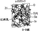
对于作为含杂质的a-IGZO结构模型的具有向其添加的1个氢原子的a-IGZO(下文称为“a-IGZO+H”)和具有向其添加的作为过剩氧的1个氧原子OEX的a-IGZO (下文称为“a-IGZO+O”)计算结构弛豫。这些原子分别位于距离图1A和1B的结构模型a-IGZO+H和a-IGZO+O中示出的氧O(A)约0.15nm的位置。For a-IGZO having 1 hydrogen atom added thereto (hereinafter referred to as "a-IGZO+H") which is a structural model of a-IGZO containing impurities and having 1 oxygen atom added thereto as excess oxygen The a-IGZO of OEX (hereinafter referred to as "a-IGZO+O") calculated the structural relaxation. These atoms are located approximately 0.15 nm away from the oxygen O(A) shown in the structural models a-IGZO+H and a-IGZO+O of FIGS. 1A and 1B , respectively.
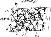
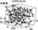
然后,对于结构弛豫后的a-IGZO+O模型计算结构弛豫,其在远离添加的氧原子OEX的位置具有另外向其添加的1个氢原子或两个氢原子(a-IGZO+OH或a-IGZO+OH2)。另外,对于该结构弛豫后的a-IGZO+O模型计算结构弛豫,其在添加的氧原子OEX附近位置具有另外向其添加的1个氢原子或两个氢原子(a-IGZO+OEXH或a-IGZO+OEXH2)。Then, the structural relaxation is calculated for the a-IGZO+O model after structural relaxation, which has one or two hydrogen atoms additionally added to it at a position away from the added oxygen atom OEX (a-IGZO+ OH or a-IGZO+OH2 ). In addition, the structural relaxation was calculated for the relaxed a-IGZO+O model, which has one or two hydrogen atoms additionally added to it near the added oxygen atom OEX (a-IGZO+ OEX H or a-IGZO+OEX H2 ).
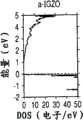
对于通过计算上述结构弛豫得到的结构模型,计算态密度(DOS)。结构模型意指a-IGZO、a-IGZO+H、a-IGZO+O、a-IGZO+OH、a-IGZO+OH2、a-IGZO+OEXH和a-IGZO+OEXH2。要注意的是,态密度(DOS)的计算中,使用400eV的截止能量和4×5×6Monkhost-Pack特殊k点网格。For the structural model obtained by calculating the above-mentioned structural relaxation, the density of states (DOS) was calculated. The structural model means a-IGZO, a-IGZO+H, a-IGZO+O, a-IGZO+OH, a-IGZO+OH2 , a-IGZO+OEX H and a-IGZO+OEX H2 . It should be noted that in the calculation of the density of states (DOS), a cut-off energy of 400eV and a special k-point grid of 4×5×6 Monkhost-Pack are used.
(计算的结果)(result of calculation)
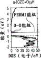
图1A~1F示出通过结构弛豫得到的上述模型的弛豫原子构造。在a-IGZO+H(图1A)中,作为杂质添加的氢与纯a-IGZO模型中存在的氧(该图中的O(A))形成键。在a-IGZO+O(图1B)中,作为过剩氧添加的氧OEX与纯a-IGZO模型中附近存在的氧(该图中的O(A))形成O-OEX键。在a-IGZO+OH(图1C)和a-IGZO+OH2(图1D)中,过剩氧维持O-OEX键,并且添加的氢与纯a-IGZO模型中附近存在的氧形成键。另一方面,在a-IGZO+OEXH(图1E)和a-IGZO+OEXH2(图1F)中,位于过剩氧附近的氢使O-OEX键断裂,并在过剩氧和氢之间形成OEX-H-O键或H-OEX-H键。特别地,从示出a-IGZO+OEXH2的图1F,可以看出H-OEX-H的结构与水相似。Figures 1A-1F show the relaxed atomic configuration of the above model obtained by structural relaxation. In a-IGZO+H (Fig. 1A), hydrogen added as an impurity forms a bond with oxygen present in the pure a-IGZO model (O(A) in this figure). In a- IGZO+O (Fig. 1B), oxygen O EX added as excess oxygen forms OOEX bonds with oxygen present nearby in the pure a-IGZO model (O(A) in this figure). In a-IGZO+OH (Fig. 1C) and a-IGZO+OH2 (Fig. 1D), the excess oxygen maintains the OOEX bond, and the added hydrogen forms a bond with the oxygen present nearby in the pure a-IGZO model. On the other hand, in a-IGZO+OEX H (Fig. 1E) and a-IGZO+OEX H2 (Fig. 1F), the hydrogen located near the excess oxygen breaks the OOEX bond, and between the excess oxygen and hydrogen OEX -HO bonds or HOEX -H bonds are formed between them. In particular, from Figure 1F showing a-IGZO+OEX H2 , it can be seen that the structure of HOEX -H is similar to water.
图2A~2G示出对于上述模型得到的DOS。另外,为了比较,示出纯a-IGZO的DOS(图2A)。在这些图中,纯a-IGZO的价带最高能量是0eV。这些图中的实线表示Fermi能级。在a-IGZO+H(图2B)的DOS中,Fermi能级位于导带中。这意味着电子作为载流子掺杂在导带中,这与氢表现出给体行为的事实相一致。在a-IGZO+O(图2C)的DOS中,Fermi能级并不存在于导带中。另外,在价带之上观察到来自O-O键的能级峰。因为该能级完全由电子占据,过剩氧并不影响n型TFT的电特性。a-IGZO+O结构模型在远离过剩氧的位置具有向其添加的氢的a-IGZO+OH(图2D)和a-IGZO+OH2(图2E)的DOS中,在价带之上观察到来自O-OEX键的峰并且Fermi能级位于导带中。过剩氧和氢彼此独立地显示出它们各自的特性,这表明存在即使过剩氧存在时过剩氧也没有起到载流子消除剂的作用的情形。另一方面,a-IGZO+O结构模型在过剩氧附近的位置具有向其添加的氢的a-IGZO+OEXH(图2F)的DOS中,在带隙中观察到来自过剩氧和氢的O-H-OEX键的陡峰。因此,从Fermi能级的位置判断,可以看出能级是未完全占据的能级。因此,能级起到捕集载流子电子的阱的作用。在a-IGZO+OEXH2(图2G)的DOS中,在a-IGZO+OEXH(图2F)中观察到的带隙中的能级消失,Fermi能级并不存在于导带中,DOS与纯a-IGZO相似。因此,在此情形中,氢不能作为大大影响TFT电性能的杂质。Figures 2A-2G show the DOS obtained for the above model. In addition, for comparison, the DOS of pure a-IGZO is shown (FIG. 2A). In these figures, the highest energy of the valence band of pure a-IGZO is 0 eV. The solid lines in these figures represent the Fermi levels. In the DOS of a-IGZO+H (Fig. 2B), the Fermi level is located in the conduction band. This implies that electrons are doped in the conduction band as carriers, which is consistent with the fact that hydrogen exhibits donor behavior. In the DOS of a-IGZO+O (Fig. 2C), the Fermi level does not exist in the conduction band. In addition, energy level peaks originating from OO bonds are observed above the valence band. Because this energy level is completely occupied by electrons, excess oxygen does not affect the electrical characteristics of n-type TFTs. The a-IGZO+O structure model is observed above the valence band in the DOS of a-IGZO+OH (Fig. 2D) and a-IGZO+OH2 (Fig. 2E) with hydrogen added to it at a position away from excess oxygen to the peak from the OOEX bond and the Fermi level is located in the conduction band. Excess oxygen and hydrogen exhibit their respective characteristics independently of each other, which indicates that there are cases where excess oxygen does not function as a carrier eliminator even when excess oxygen exists. On the other hand, in the DOS of a-IGZO+OEX H (Fig. 2F) where the a-IGZO+O structure model has hydrogen added to it at a position near the excess oxygen, the band gap from excess oxygen and hydrogen is observed The steep peak of the OHOEX bond. Therefore, judging from the position of the Fermi energy level, it can be seen that the energy level is an incompletely occupied energy level. Thus, the energy levels act as traps for the carrier electrons. In the DOS of a-IGZO+OEX H2 (Fig. 2G), the energy levels in the band gap observed in a-IGZO+OEX H (Fig. 2F) disappear, and the Fermi level does not exist in the conduction band , DOS was similar to pure a-IGZO. Therefore, in this case, hydrogen cannot act as an impurity that greatly affects the electrical properties of the TFT.
由上可知,虽然实验事实表明非晶氧化物半导体中的氢起到给体的作用,但存在于膜中的氢原子的浓度并不与载流子电子密度良好吻合,据认为该事实的原因如下。通过向非晶氧化物半导体薄膜注入离子而引入氢的情形对应于上述的a-IGZO+H的情形,并且将氢离子化以起到给体的作用。另一方面,表明在利用受控的氧分压或水分压而形成的薄膜中,存在于膜中的大部分氢并未起到给体的作用。由上述计算可知,当具有组成比不同于a-IGZO中其化学计量组成比的过剩氧与氢形成化学键O-H-OEX或OEX-H2时,氢并未起到给体的作用。在此情形中,O-H-OEX起到载流子阱的作用,而OEX-H2不影响TFT的电性能。因此认为在形成的膜中,因为大比例存在的氢以O-H-OEX或OEX-H2的键合状态存在,保持了实现常闭TFT器件的载流子电子密度。From the above, although the experimental facts show that hydrogen in the amorphous oxide semiconductor functions as a donor, the concentration of hydrogen atoms present in the film does not coincide well with the carrier electron density, and it is considered that the reason for this fact is as follows. The case of introducing hydrogen by implanting ions into the amorphous oxide semiconductor thin film corresponds to the above-mentioned case of a-IGZO+H, and the hydrogen is ionized to function as a donor. On the other hand, it has been shown that most of the hydrogen present in the film does not function as a donor in a thin film formed using a controlled oxygen partial pressure or water pressure. From the above calculations, it can be seen that when excess oxygen with a composition ratio different from its stoichiometric composition ratio in a-IGZO forms a chemical bond with hydrogen OHOEX or OEX -H2 , hydrogen does not act as a donor. In this case, OHOEX functions as a carrier trap, while OEX -H2 does not affect the electrical properties of TFTs. It is therefore considered that in the formed film, since a large proportion of hydrogen present exists in the bonding state of OHOEX or OEX -H2 , the carrier electron density to realize normally-off TFT devices is maintained.
本文中使用的过剩氧并不意味着氧与整个非晶氧化物半导体中的其化学计量组成比相比过剩,而是意指氧在非晶氧化物半导体一部分中作为单位尺寸的具有特定数目原子的微区中过剩。因此,即使当氧根据其化学计量组成比存在于整个非晶氧化物半导体中时,如果氧缺乏的量和过剩氧的量程度相同,则具有本文中所用的过剩氧。Excess oxygen as used herein does not mean that oxygen is excess compared to its stoichiometric composition ratio in the entire amorphous oxide semiconductor, but means that oxygen is present in a part of the amorphous oxide semiconductor as a specific number of atoms per unit size. Excess in the micro-area. Therefore, even when oxygen exists in the entire amorphous oxide semiconductor according to its stoichiometric composition ratio, if the amount of oxygen deficiency and the amount of excess oxygen are the same degree, there is excess oxygen as used herein.
具体地,过剩氧的存在意指尽管氧与金属元素M(M为In、Zn或Ga)键合并且键合状态为M-O-M,但该键合状态实际上为包括O-O的M-O-O-M。氧的该键合状态表示为O-OEX键。当氢与该O-OEX键键合时,键合状态表示为OEX-H或H-OEX-H。Specifically, the presence of excess oxygen means that although oxygen is bonded to the metal element M (M is In, Zn, or Ga) and the bonding state is MOM, the bonding state is actually MOOM including OO. This bonding state of oxygen is expressed as OOEX bond. When hydrogen is bonded to this OOEX bond, the bonding state is expressed as OEX -H or HOEX -H.
本文中使用的O-H键意指上述的a-IGZO+OH键。另外,由与其相对于金属元素的化学计量组成比相比过剩氧和氢形成的OEX-H键意指具有将氢插入过剩氧的O-OEX键中的结构的上述a-IGZO+OEXH键。另外,由过剩氧和氢形成的H-OEX-H键意指上述的a-IGZO+OEXH2键。The OH bond used herein means the aforementioned a-IGZO+OH bond. In addition, the OEX -H bond formed by excess oxygen and hydrogen compared to its stoichiometric composition ratio with respect to the metal element means the above-mentioned a-IGZO+OEX H having a structure in which hydrogen is inserted into the OOEX bond of excess oxygen key. In addition, the HOEX -H bond formed by excess oxygen and hydrogen means the aforementioned a-IGZO+OEX H2 bond.
如上所述,已经发现当氢附近的氧局部过剩时非晶氧化物半导体中的氢没有起到给体的作用。具体地,在含有相对于载流子密度过剩氢的非晶氧化物半导体中,作为载流子源的a-IGZO+OH键的数目决定非晶氧化物半导体的最终载流子密度。换句话说,O-H键的密度为载流子密度。As described above, it has been found that hydrogen in an amorphous oxide semiconductor does not function as a donor when oxygen in the vicinity of hydrogen is locally excessive. Specifically, in an amorphous oxide semiconductor containing excess hydrogen relative to the carrier density, the number of a-IGZO+OH bonds as a carrier source determines the final carrier density of the amorphous oxide semiconductor. In other words, the density of O-H bonds is the carrier density.
当大量(大于等于1×1020cm-3)的氢原子包含在非晶氧化物半导体中时,重要的是当非晶氧化物半导体中吸收过剩氧原子和氢原子时,过剩氧原子数与氢原子数的比例大于等于1∶2。按此方式,可以含有大于等于5×1019cm-3过剩氧原子并且载流子密度可以为1×1018cm-3,这足以起到TFT的沟道层半导体的作用。当氢原子数小于1×1020cm-3时,由于氢以外的载流子源例如氧缺乏产生的载流子密度与由于O-H键产生的载流子密度竞争(密度差变小),因此存在并未保持根据本发明的关系的情形(O-H键的密度落在根据本发明的范围之外),这是不优选的。When a large amount (1×1020 cm-3 or more) of hydrogen atoms is contained in the amorphous oxide semiconductor, it is important that when excess oxygen atoms and hydrogen atoms are absorbed in the amorphous oxide semiconductor, the number of excess oxygen atoms is equal to The ratio of the number of hydrogen atoms is greater than or equal to 1:2. In this way, excess oxygen atoms of 5×1019 cm-3 or more can be contained and the carrier density can be 1×1018 cm-3 , which is sufficient to function as a channel layer semiconductor of TFT. When the number of hydrogen atoms is less than 1×1020 cm-3 , the carrier density due to carrier sources other than hydrogen, such as oxygen deficiency, competes with the carrier density due to OH bonds (the density difference becomes smaller), so There are cases where the relationship according to the present invention is not maintained (the density of OH bonds falls outside the range according to the present invention), which is not preferable.
另外,当大量(大于等于1×1021cm-3)的氢原子包含在非晶氧化物半导体中时,起到载流子阱作用的O-H-OEX的浓度增加。为了抑制该阱的增加,更重要的是向作为溅射气体的Ar气不添加氧而是只添加水蒸汽。作为例子,可以通过向Ar气只添加水蒸汽来形成溅射气体。图3示出由测定根据该实施方案制备的a-IGZO的Hall效应得到的载流子密度、Hall迁移率和电阻率对于通过溅射形成膜时水蒸汽分压的依赖性。取决于溅射成膜的条件例如气体压力和施加电力的密度,通过引入高于或等于1×10⁻²Pa的水蒸汽分压,a-IGZO的电阻率可以增加。另外,可以使载流子密度小于等于1×1018cm-3。氢量的上限为1×1022cm-3。设定此上限是因为难以通过水蒸汽向非晶氧化物半导体薄膜稳定地提供更多的氢。另外,因为起到载流子阱作用的O-H-OEX的密度变得更高,不可能得到对于TFT操作必需的电特性。例如,TFT的阈值变得极高。In addition, when a large amount (1×1021 cm-3 or more) of hydrogen atoms is contained in the amorphous oxide semiconductor, the concentration of OHOEX that functions as a carrier trap increases. In order to suppress the increase of the traps, it is more important to add only water vapor instead of oxygen to the Ar gas as the sputtering gas. As an example, sputtering gas can be formed by adding only water vapor to Ar gas. FIG. 3 shows the dependence of carrier density, Hall mobility, and resistivity on water vapor partial pressure at the time of film formation by sputtering, obtained by measuring the Hall effect of a-IGZO prepared according to this embodiment. The resistivity of a-IGZO can be increased by introducing a partial pressure of water vapor higher than or equal to 1×10⁻² Pa depending on conditions of sputtering film formation such as gas pressure and density of applied power. In addition, the carrier density can be made equal to or less than 1×1018 cm-3 . The upper limit of the amount of hydrogen is 1×1022 cm-3 . This upper limit is set because it is difficult to stably supply more hydrogen to the amorphous oxide semiconductor thin film by water vapor. In addition, since the density of OHOEX functioning as a carrier trap becomes higher, it is impossible to obtain electrical characteristics necessary for TFT operation. For example, the threshold of TFT becomes extremely high.
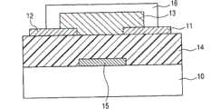
图4是根据该实施方案制备的TFT器件的结构示意图。通过在基板10上依次设置栅电极15、栅绝缘膜14、源电极12和漏电极11、沟道层13和保护层16而形成TFT器件。Fig. 4 is a schematic structural view of a TFT device prepared according to this embodiment. A TFT device is formed by sequentially disposing a
可应用于本发明的半导体器件的结构并不限于如上所述的底栅结构的TFT。例如,TFT可以具有其中在栅电极上依次设置栅绝缘膜和半导体沟道层,然后在其上形成源电极和漏电极的逆交错(reversestagger)结构,或者可以具有作为上下颠倒的逆交错结构的交错结构(顶栅结构)。The structure of the semiconductor device applicable to the present invention is not limited to the TFT of the bottom gate structure as described above. For example, a TFT may have a reverse stagger structure in which a gate insulating film and a semiconductor channel layer are sequentially provided on a gate electrode, and then a source electrode and a drain electrode are formed thereon, or may have a reverse stagger structure that is upside down. Staggered structure (top gate structure).
根据本发明的发明人的发现,优选使用含有In与Zn中至少一种元素和氢的非晶氧化物半导体层作为沟道层的薄膜晶体管取决于组成而具有如下特性:当使用具有大于约10Ωcm且小于约1×10⁶Ωcm的电阻率的半绝缘氧化物膜时,可以得到令人满意的TFT特性。例如,当电阻率小于等于10Ωcm时,不可能得到常闭晶体管或大的开/关比。在极端的情况中,即使施加栅电压时,源电极和漏电极之间的电流没有打开/关闭,晶体管未工作。另一方面,当电阻率大于等于1×106Ωcm时,不可能得到大的开电流。在极端的情况中,即使施加栅电压时,源电极和漏电极之间的电流没有打开/关闭,晶体管未工作。According to the findings of the inventors of the present invention, it is preferable that a thin film transistor using an amorphous oxide semiconductor layer containing at least one element of In and Zn and hydrogen as a channel layer has the following characteristics depending on the composition: when using Satisfactory TFT characteristics can be obtained with a semi-insulating oxide film having a resistivity of less than about 1×10⁶ Ωcm. For example, when the resistivity is 10 Ωcm or less, it is impossible to obtain a normally-off transistor or a large on/off ratio. In extreme cases, even when the gate voltage is applied, the current between the source electrode and the drain electrode is not turned on/off, and the transistor does not work. On the other hand, when the resistivity is 1×10⁶ Ωcm or more, it is impossible to obtain a large on-current. In extreme cases, even when the gate voltage is applied, the current between the source electrode and the drain electrode is not turned on/off, and the transistor does not work.
通常,通过形成膜时引入的氧分压来控制氧化物的电阻率和载流子密度。更具体地,通过控制氧分压,主要控制薄膜中氧缺乏的量,由此来控制电子载流子密度。但是,根据本发明,通过仅控制图3中所示的水蒸汽分压来控制电子载流子密度。In general, the resistivity and carrier density of the oxide are controlled by the partial pressure of oxygen introduced when forming the film. More specifically, by controlling the oxygen partial pressure, the amount of oxygen deficiency in the film is mainly controlled, thereby controlling the electron carrier density. However, according to the present invention, the electron carrier density is controlled by controlling only the water vapor partial pressure shown in FIG. 3 .
以下详细说明根据本发明的形成沟道层的方法。The method of forming a channel layer according to the present invention will be described in detail below.
首先,制备由玻璃等制成的基板10。利用气相法例如DC溅射、RF溅射、脉冲激光沉积、原子层沉积或电子束沉积、其组合等,形成非晶氧化物半导体膜。此处,在非晶氧化物半导体膜的电阻率高于得到TFT沟道层的满意特性的电阻率的条件下形成膜。这基本上通过取决于非晶氧化物半导体膜的组成和成膜装置,将引入的水蒸汽分压设定在高于或等于8×10⁻⁴Pa的范围内来实现。特别地,当引入的水蒸汽的分压高于或等于1×10⁻²Pa时,这可以容易地实现。当使用真空装置成膜时,引入的水蒸汽的分压的上限为成膜气体的压力。为了防止由于气相中聚合导致的膜的密度下降和成膜速度下降,希望引入的水蒸汽的分压为约10Pa或更低。为了严格控制电阻率,可同时引入并控制水蒸汽和其量比水蒸汽小的氧。First, a
本文中使用的引入的水蒸汽的分压意指通过流速控制器有意引入成膜装置的水蒸汽的分压。从成膜装置等的内壁不可避免地释放的水蒸汽、因为成膜装置泄漏而从外部进入的水蒸汽和从靶释放的水蒸汽取决于成膜历史而大幅变化,因此非常难于控制。使真空成膜装置的背压为低于或等于1×10⁻⁸Pa的超高真空并控制非晶氧化物中的氢浓度小于载流子密度在技术上是可能的。但是,如果这样做,会产生使制造成本增加的问题,包括增加的成膜装置的成本和延长的制造间歇时间。但是,当剩余水蒸汽的压力超过引入的水蒸汽的分压的上限时,难以得到本发明的效果,因此优选本发明中使用的成膜装置的背压低于或等于5×10⁻⁴Pa。要指出的是,流速控制器是例如质流控制器。The partial pressure of the introduced water vapor used herein means the partial pressure of the water vapor intentionally introduced into the film forming apparatus by a flow rate controller. The water vapor unavoidably released from the inner wall of the film forming apparatus, etc., the water vapor entering from the outside due to the leakage of the film forming apparatus, and the water vapor released from the target vary greatly depending on the film forming history, so it is very difficult to control. It is technically possible to make the back pressure of the vacuum film forming device an ultra-high vacuum lower than or equal to 1×10⁻⁸ Pa and control the hydrogen concentration in the amorphous oxide to be smaller than the carrier density. However, if this is done, there arises a problem of increasing the manufacturing cost, including an increased cost of a film-forming apparatus and an extended manufacturing tact time. However, when the pressure of the remaining water vapor exceeds the upper limit of the partial pressure of the introduced water vapor, it is difficult to obtain the effect of the present invention, so it is preferable that the back pressure of the film forming apparatus used in the present invention is lower than or equal to 5×10⁻⁴ Pa. It is pointed out that the flow rate controller is eg a mass flow controller.
另外,此处从TFT器件性能的观点考虑,优选在非晶氧化物半导体膜的电阻率大于或等于1×10²Ωcm的条件下成膜。要指出的是,根据本发明,金属膜形成后,取决于氧化物膜的组成和成膜条件,电阻率的下限例如为大于或等于1×10Ωcm。Here, from the viewpoint of TFT device performance, it is preferable to form the amorphous oxide semiconductor film under the condition that the resistivity of the amorphous oxide semiconductor film is equal to or greater than 1×10² Ωcm. It should be noted that, according to the present invention, after the metal film is formed, the lower limit of the resistivity is, for example, greater than or equal to 1×10 Ωcm depending on the composition of the oxide film and the film forming conditions.
之后,可以对制备的非晶氧化物半导体膜进行热处理。此处,设定热处理条件以使非晶氧化物半导体膜具有使TFT沟道层获得满意特性的电阻率。为了在短时间内均匀控制电阻率,可以在气氛温度为150℃~500℃、优选200℃~350℃下进行热处理。另外,从均匀性的观点考虑,使用氧化气氛有效,因此这也是优选的。After that, heat treatment may be performed on the prepared amorphous oxide semiconductor film. Here, the heat treatment conditions are set so that the amorphous oxide semiconductor film has a resistivity for obtaining satisfactory characteristics of the TFT channel layer. In order to uniformly control the resistivity in a short time, heat treatment may be performed at an atmosphere temperature of 150°C to 500°C, preferably 200°C to 350°C. In addition, from the viewpoint of uniformity, it is effective to use an oxidizing atmosphere, so this is also preferable.
当进行热处理时,据认为有如下现象发生:在非晶氧化物中使氢原子热扩散;扩散的氢与起到载流子阱作用的O-H-OEX键合以产生不影响TFT电特性的OEX-H2;并使载流子阱密度降低。When heat treatment is performed, it is considered that the following phenomena occur: thermal diffusion of hydrogen atoms in the amorphous oxide; diffused hydrogen bonds with OHOEX that acts as a carrier trap to generate OEX that does not affect the electrical characteristics of TFT -H2 ; and reduce the carrier trap density.
以低成本形成TFT的优选方法是通过施涂溶液来形成非晶氧化物半导体膜。例如,首先,通过喷墨印刷施涂溶解在作为溶剂的2-甲氧基乙醇中的Zn(CH3COO)22H2O(可由Aldrich得到)和In(CH3COO)3(可由Aldrich得到)的溶液作为材料。然后,在低于或等于500℃温度的气氛中进行热处理以得到非晶InZnO膜。为了充分地挥发溶剂,可以在150℃~500℃下、优选在200℃~350℃下进行热处理。热处理的温度的上限受氧化物半导体膜的结晶化限制。此处,大于或等于1×1020cm-3的氢原子残留在非晶氧化物半导体膜中,并且可以实现获得本发明载流子密度的小于或等于1×1018cm-3的M-OH键数。电沉积可以用作使用其它溶剂的成膜方法。例如,利用含有硝酸铟、硝酸镓、硝酸锌和二甲胺-硼烷(DMAB)的水溶液作为原料,可以在绝缘基板(例如,Corning 1737)上形成In-Ga-Zn-O基非晶氧化物薄膜。在对其未施加电场的情况下沉积起始沉积层后,可以使用不含二甲胺-硼烷(DMAB)的水溶液并且使用外部电力施加电场以通过电沉积形成非晶氧化物膜。此处,水溶液的温度是60℃。此处以此方式形成的非晶氧化物膜具有大量(大于或等于1×1020cm-3)的残留氢原子。通过在低于或等于500℃下热处理该膜,可以实现本发明中的小于或等于1×1018cm-3的M-OH键数以及小于或等于1×1018cm-3的载流子密度。以此方式,可以形成可作为TFT工作的非晶氧化物半导体膜。为了使包含在膜中的大量的水分挥发,可以在150℃~500℃下、优选在200℃~350℃下进行热处理。热处理的温度上限受氧化物半导体膜的结晶化限制。A preferable method of forming TFTs at low cost is to form an amorphous oxide semiconductor film by applying a solution. For example, first, Zn(CH3 COO)2 2H2 O (available from Aldrich) and In(CH3 COO)3 (available from Aldrich ) dissolved in 2-methoxyethanol as solvent are applied by inkjet printing. ) solution as the material. Then, heat treatment is performed in an atmosphere at a temperature lower than or equal to 500° C. to obtain an amorphous InZnO film. In order to sufficiently volatilize the solvent, heat treatment may be performed at 150°C to 500°C, preferably at 200°C to 350°C. The upper limit of the heat treatment temperature is limited by the crystallization of the oxide semiconductor film. Here, hydrogen atomsgreater than or equal to 1×1020 cm-3 remain in the amorphous oxide semiconductor film,and M- Number of OH bonds. Electrodeposition can be used as a film-forming method using other solvents. For example, using an aqueous solution containing indium nitrate, gallium nitrate, zinc nitrate, and dimethylamine-borane (DMAB) as raw materials, an In-Ga-Zn-O-based amorphous oxide can be formed on an insulating substrate (e.g., Corning 1737). object film. After the initial deposition layer is deposited without applying an electric field thereto, an aqueous solution not containing dimethylamine-borane (DMAB) can be used and an electric field is applied using external power to form an amorphous oxide film by electrodeposition. Here, the temperature of the aqueous solution was 60°C. The amorphous oxide film formed in this way here has a large amount (greater than or equal to 1×1020 cm−3 ) of residual hydrogen atoms. The number of M-OH bonds less than or equal to 1×1018 cm-3 and the number of carriers less than or equal to 1×1018 cm-3 in the present invention can be achieved by heat-treating the film at less than or equal to 500°C density. In this way, an amorphous oxide semiconductor film operable as a TFT can be formed. In order to volatilize a large amount of moisture contained in the film, heat treatment may be performed at 150°C to 500°C, preferably at 200°C to 350°C. The upper limit of the heat treatment temperature is limited by the crystallization of the oxide semiconductor film.
然后,通过在含氧的气氛中溅射形成氧化物绝缘体保护膜,由其可以抵消由于保护膜的形成对沟道层的损伤和还原效果。Then, an oxide insulator protective film is formed by sputtering in an atmosphere containing oxygen, whereby the damage and reduction effect on the channel layer due to the formation of the protective film can be counteracted.
以下对TFT结构的部件进行详细说明。The components of the TFT structure will be described in detail below.
(栅极绝缘层)(gate insulating layer)
在本发明中,希望将SiO2用于栅极绝缘层。或者,也优选将含有SiO2、Y2O3、Al2O3、HfO2和TiO2中至少一种的材料用于栅极绝缘层。也可使用其中将这些层层叠的任何膜。In the present invention, it is desirable to useSiO2 for the gate insulating layer. Alternatively, a material containing at least one of SiO2 , Y2 O3 , Al2 O3 , HfO2 and TiO2 is also preferably used for the gate insulating layer. Any film in which these layers are laminated can also be used.
作为栅极绝缘层的成膜方法,可使用气相法例如溅射、脉冲激光沉积和电子束沉积。但成膜方法并不限于这些方法。As a film-forming method of the gate insulating layer, a vapor phase method such as sputtering, pulse laser deposition, and electron beam deposition can be used. However, the film-forming method is not limited to these methods.
(电极)(electrode)
对用于源电极、漏电极和栅电极的材料无特别限制,只要这些材料能使满意的导电性和与沟道层的满意的电连接实现。例如,可使用由In2O3:Sn或ZnO形成的透明导电膜和由Mo、Au、Pt、Al、Ni和Cu形成的金属膜。此外,为了提高粘合性,可以在沟道层或绝缘层和电极之间设置由Ti、Ni、Cr等形成的层。There are no particular limitations on the materials used for the source electrode, drain electrode, and gate electrode as long as they enable satisfactory electrical conductivity and satisfactory electrical connection with the channel layer. For example, a transparent conductive film formed of In2 O3 :Sn or ZnO and a metal film formed of Mo, Au, Pt, Al, Ni, and Cu can be used. In addition, in order to improve adhesion, a layer formed of Ti, Ni, Cr, or the like may be provided between the channel layer or the insulating layer and the electrode.
(基板)(substrate)
作为基板,取决于沟道层的热处理条件等可以使用玻璃基板、金属基板、塑料基板、塑料膜等。As the substrate, a glass substrate, a metal substrate, a plastic substrate, a plastic film, or the like can be used depending on heat treatment conditions and the like of the channel layer.
(沟道层)(channel layer)
沟道层是含有In和Zn中至少一种元素和氢的非晶氧化物。The channel layer is an amorphous oxide containing at least one element of In and Zn and hydrogen.
作为沟道层的成膜方法,可以使用气相法例如溅射、脉冲激光沉积和电子束沉积。但是成膜方法并不限于这些方法。As a film-forming method of the channel layer, a vapor phase method such as sputtering, pulse laser deposition, and electron beam deposition can be used. However, the film-forming method is not limited to these methods.
为了确保在非晶氧化物半导体中吸收固定量的氢,并因此为了防止在成膜开始前水蒸汽被吸附到沟道层的底层或真空装置的腔室壁,希望在高于或等于80℃下形成沟道层。In order to ensure that a fixed amount of hydrogen is absorbed in the amorphous oxide semiconductor, and thus to prevent water vapor from being adsorbed to the bottom layer of the channel layer or the chamber wall of the vacuum device before the start of film formation, it is desirable to operate at 80°C or higher. A channel layer is formed underneath.
希望热处理的温度等于或低于玻璃化转变温度,并且在本发明中,希望热处理的温度为150℃~500℃。热处理温度的下限是150℃,因为作为将金属铟从中精制时使用的公知材料,In(OH)3的分解在150℃开始。从缩短热处理时间的观点考虑,优选热处理温度在200℃~350℃。The temperature of the heat treatment is desirably equal to or lower than the glass transition temperature, and in the present invention, the temperature of the heat treatment is desirably 150°C to 500°C. The lower limit of the heat treatment temperature is 150°C because decomposition of In(OH)3 , which is a well-known material used when metal indium is refined therefrom, starts at 150°C. From the viewpoint of shortening the heat treatment time, the heat treatment temperature is preferably 200°C to 350°C.
因为可以通过使用形成沟道层的温度进行热处理,可以在形成沟道层的同时进行热处理。另外,可以在形成保护膜后或在完成TFT后进行热处理。Since the heat treatment can be performed by using the temperature at which the channel layer is formed, the heat treatment can be performed simultaneously with the formation of the channel layer. In addition, heat treatment may be performed after forming the protective film or after completing the TFT.
(保护膜)(protective film)
作为保护膜,使用含有至少一种金属元素的金属氧化物膜。在金属氧化物中,作为保护膜,优选使用含有以下中至少一种的物质:SiO2、Al2O3、Ga2O3、In2O3、MgO、CaO、SrO、BaO、ZnO、Nb2O5、Ta2O5、TiO2、ZrO2、HfO2、CeO2、Li2O、Na2O、K2O、Rb2O、Sc2O3、Y2O3、La2O3、Nd2O3、Sm2O3、Gd2O3、Dy2O3、Er2O3和Yb2O3。As the protective film, a metal oxide film containing at least one metal element is used. Among metal oxides, as a protective film, it is preferable to use a substance containing at least one of the following: SiO2 , Al2 O3 , Ga2 O3 , In2 O3 , MgO, CaO, SrO, BaO, ZnO, Nb2 O5 , Ta2 O5 ,
或者,除这些金属氧化物外,还可以使用硅氧氮化物(SiOxNy)。Alternatively, silicon oxynitride (SiOx Ny ) may be used in addition to these metal oxides.
作为在TFT上形成上述金属氧化物或SiOxNy作为保护膜的方法,可以使用化学气相沉积(CVD)、溅射等。当通过溅射形成保护膜时,在含氧的气氛中溅射期间进行成膜。这是因为其中例如在Ar气气氛中形成保护膜的器件与保护膜形成之前相比,在TFT特性上劣化。可以想象,TFT特性劣化的原因是由于保护膜形成期间从沟道层界面的氧释放导致载流子产生而造成沟道层电阻的下降。因此,在溅射保护膜期间要求在含氧的气氛中进行成膜。全部溅射气体中氧含量希望为10%~80%。As a method of forming the above-mentioned metal oxide orSiOxNy as a protective film on the TFT, chemical vapor deposition (CVD), sputtering,or the like can be used. When the protective film is formed by sputtering, film formation is performed during sputtering in an oxygen-containing atmosphere. This is because a device in which a protective film is formed, for example, in an Ar gas atmosphere is degraded in TFT characteristics as compared with before the protective film is formed. It is conceivable that the reason for the deterioration of TFT characteristics is a decrease in channel layer resistance due to carrier generation due to oxygen release from the channel layer interface during formation of the protective film. Therefore, film formation in an oxygen-containing atmosphere is required during sputtering of the protective film. The oxygen content in the entire sputtering gas is desired to be 10% to 80%.
(TFT特性)(TFT characteristics)
图5示出本发明的TFT的典型传输特性(Vg-Id特性)。在源电极和漏电极之间施加12V的电压Vd时,通过在-20V和20V之间扫过栅电压Vg,可以控制源电极和漏电极之间的电流Id(开闭)。FIG. 5 shows typical transfer characteristics (Vg-Id characteristics) of the TFT of the present invention. When a voltage Vd of 12V is applied between the source electrode and the drain electrode, by sweeping the gate voltage Vg between -20V and 20V, the current Id between the source electrode and the drain electrode can be controlled (on-off).
特别地,当将本发明应用于使用由于无粒界散射和优异的界面特性而最初具有高载流子迁移率的非晶氧化物作为沟道层的TFT时,可以实现具有高场效应迁移率和优异特性的TFT。在此情形中,通过在氧化物膜中引入Ga和Sn中至少一种元素将非晶相稳定化。此外,从将非晶相稳定化的观点出发,可以想到将热处理时的氧化气氛的温度优选设定在低于或等于500℃。In particular, when the present invention is applied to a TFT using an amorphous oxide that initially has high carrier mobility due to no grain boundary scattering and excellent interfacial properties as a channel layer, it is possible to achieve a high field-effect mobility and TFT with excellent characteristics. In this case, the amorphous phase is stabilized by introducing at least one element of Ga and Sn into the oxide film. In addition, from the viewpoint of stabilizing the amorphous phase, it is conceivable that the temperature of the oxidizing atmosphere during the heat treatment is preferably set to be lower than or equal to 500°C.
此处,通过以下观测可以识别非晶状态:当以约0.5度的低入射角将X射线衍射到作为测试目标的薄膜时,没有检测到明显的衍射峰(换句话说,观测到光晕图案)。应当指出的是,当将上述材料用于薄膜晶体管的沟道层时,本发明并未排除沟道层含有微晶态组分材料的情形。Here, the amorphous state can be identified by the observation that when X-rays are diffracted onto a thin film as a test target at a low incident angle of about 0.5 degrees, no distinct diffraction peaks are detected (in other words, a halo pattern is observed ). It should be noted that when the above-mentioned materials are used for the channel layer of a thin film transistor, the present invention does not exclude the case that the channel layer contains a microcrystalline component material.
通过将显示器件例如有机或无机电致发光(EL)器件或者液晶器件的电极连接到作为上述薄膜晶体管输出终端的漏电极,可以形成显示装置。以下参照显示装置的剖面图说明显示装置结构的具体例子。A display device can be formed by connecting an electrode of a display device such as an organic or inorganic electroluminescence (EL) device or a liquid crystal device to a drain electrode as an output terminal of the above-mentioned thin film transistor. A specific example of the structure of the display device will be described below with reference to cross-sectional views of the display device.
图6为作为本发明的另一实施方案的示例性显示装置的剖面图。在基板611上形成TFT。TFT包括栅电极612、栅绝缘膜613、非晶氧化物半导体膜614、保护层615、源(漏)电极616和漏(源)电极617。FIG. 6 is a cross-sectional view of an exemplary display device as another embodiment of the present invention. TFTs are formed on the substrate 611 . The TFT includes a gate electrode 612 , a gate insulating film 613 , an amorphous oxide semiconductor film 614 , a protective layer 615 , a source (drain) electrode 616 , and a drain (source) electrode 617 .
将电极618经中间层绝缘膜619连接到漏(源)电极617。电极618与发射层620接触。发射层620与电极621接触。The electrode 618 is connected to the drain (source) electrode 617 via the interlayer insulating film 619 . Electrode 618 is in contact with emissive layer 620 . The emission layer 620 is in contact with the electrode 621 .
以这样的结构,可以利用经过在非晶氧化物半导体膜614中形成的沟道由源(漏)电极616通入漏(源)电极617的电流值来控制注入发射层620中的电流。With such a structure, the current injected into the emitter layer 620 can be controlled by the value of the current passed from the source (drain) electrode 616 to the drain (source) electrode 617 through the channel formed in the amorphous oxide semiconductor film 614 .
因此,可以通过TFT的栅电极612处的电压控制电流。此处,电极618、发射层620和电极621形成无机或有机电致发光器件。Therefore, the current can be controlled by the voltage at the gate electrode 612 of the TFT. Here, the electrode 618, the emissive layer 620 and the electrode 621 form an inorganic or organic electroluminescent device.
图7是作为本发明另一实施方案的另一示例性显示装置的剖面图。将漏(源)电极717延长以致也作为电极718。可以将电极723和对电极718做成将电压施加到夹设在高电阻膜720和722之间的液晶单元或者电泳颗粒单元721的结构。图7也示出基板711、栅绝缘膜713、保护层715和中间层绝缘膜719。FIG. 7 is a cross-sectional view of another exemplary display device as another embodiment of the present invention. The drain (source) electrode 717 is extended so as to also serve as the electrode 718 . The
液晶单元或电泳颗粒单元721、高电阻膜720和722、电极718和电极723形成显示器件。The liquid crystal unit or
可以通过经过在非晶氧化物半导体膜714中形成的沟道由源电极716通入漏电极717的电流值控制施加到显示器件的电压。The voltage applied to the display device can be controlled by the value of the current passed from the
因此,可以利用TFT的栅电极712处的电压控制电压。此处,当显示器件的显示介质是具有封装在其绝缘膜中的流体和颗粒的封装体时,可以省去高电阻膜720和722。Therefore, the voltage can be controlled using the voltage at the
以上对作为具有底栅逆交错结构的TFT的两个实例TFT进行了说明,但本发明并不限于这样的结构。The above has explained two example TFTs as TFTs having a bottom-gate inverse staggered structure, but the present invention is not limited to such a structure.
例如,只要在作为TFT的输出终端的漏电极和显示器件之间的连接拓扑上相同,其它结构例如共平面结构也可以。For example, other structures such as a coplanar structure are also possible as long as the connection topology between the drain electrode which is the output terminal of the TFT and the display device is the same.
另外,在上述的两个实例TFT中,用于驱动显示器件的成对的电极设置成与基板平行,但是本发明并不限于这样的结构。In addition, in the two example TFTs described above, the paired electrodes for driving the display device are arranged parallel to the substrate, but the present invention is not limited to such a structure.
例如,只要作为TFT的输出终端的漏电极和显示器件之间的连接拓扑上相同,可以将电极的一个或两个设置成与基板垂直。For example, one or both of the electrodes may be arranged perpendicular to the substrate as long as the connection between the drain electrode as the output terminal of the TFT and the display device is topologically the same.
另外,关于上述两个实例TFT,只有一个TFT示出与显示器件相连,但本发明并不限于这样的结构。例如,在图中示出的TFT还可以与根据本发明的另一TFT连接,只要图中示出的TFT在包括这些TFT的电路的最后阶段。In addition, with regard to the above two example TFTs, only one TFT is shown connected to the display device, but the present invention is not limited to such a structure. For example, a TFT shown in the drawing can also be connected with another TFT according to the present invention as long as the TFT shown in the drawing is at the final stage of a circuit including these TFTs.
此处,当用于驱动显示器件的成对电极设置成与基板平行时,如果显示器件是反射显示器件例如EL器件或反射液晶器件,要求电极的任意一个对发射光或反射光的波长透明。Here, when a pair of electrodes for driving a display device is arranged parallel to a substrate, if the display device is a reflective display device such as an EL device or a reflective liquid crystal device, either one of the electrodes is required to be transparent to the wavelength of emitted light or reflected light.
如果显示器件是透射显示器件例如透射液晶器件,要求两个电极对透射光透明。If the display device is a transmissive display device such as a transmissive liquid crystal device, both electrodes are required to be transparent to transmitted light.
另外,在根据此实施方案的TFT中,所有部件可以是透明的以致可以形成透明显示器件。In addition, in the TFT according to this embodiment, all components can be transparent so that a transparent display device can be formed.
另外,可以在具有低热阻的基板例如轻质、柔性并且透明的塑料树脂基板上设置这样的显示器件。In addition, such a display device can be provided on a substrate having low thermal resistance such as a lightweight, flexible and transparent plastic resin substrate.
其次,参照图8说明两维地布置多个包括EL器件(此处,为有机EL器件)和薄膜晶体管的像素的显示装置。Next, a display device in which a plurality of pixels including EL devices (here, organic EL devices) and thin film transistors are two-dimensionally arranged will be described with reference to FIG. 8 .
在图8中,晶体管801驱动有机EL层804。晶体管802选择像素。电容器803保持选择的状态,在共通电极线807和晶体管802的源之间保持电荷,并保持晶体管801的栅信号。通过扫描电极线805和信号电极线806选择像素。In FIG. 8 , a
更具体地,将图像信号作为脉冲信号从驱动电路(未示出)经扫描电极线805施加到栅电极。同时,还施加信号作为从另一驱动电路(未示出)经信号电极线806到晶体管802的脉冲信号以选择像素。此处,打开晶体管802并且在信号电极线806和晶体管802的电源之间的电容器803中储存电荷。More specifically, an image signal is applied as a pulse signal from a drive circuit (not shown) to the gate electrode via the
这使晶体管801的栅保持在希望的电压并且将晶体管801打开。将此状态维持到接收下一信号。This keeps the gate of
在晶体管801打开的期间,持续向有机EL层804供给电压和电流并且维持发光。While the
尽管图8中示出的结构每个像素具有两个晶体管和一个电容器,为了提高性能可以引入更多的晶体管等。Although the structure shown in FIG. 8 has two transistors and one capacitor per pixel, more transistors, etc. may be introduced to improve performance.
必要的是:通过使用透明并且可以在低温下形成的In-Ga-Zn-O基TFT用于晶体管部分,可以得到有效的EL器件。It is necessary that an efficient EL device can be obtained by using an In-Ga-Zn-O-based TFT which is transparent and can be formed at a low temperature for the transistor part.
尽管以下参照实施例进一步说明本发明,但本发明并不限于此。Although the present invention is further described below with reference to examples, the present invention is not limited thereto.
(实施例1)(Example 1)
在该实施例中,对本发明的TFT器件的实施方案进行说明。In this example, an embodiment of the TFT device of the present invention is described.
首先,在玻璃基板上形成In-Ga-Zn-O膜作为非晶氧化物半导体。通过DC溅射成膜在氩气氛中形成In-Ga-Zn-O膜。First, an In-Ga-Zn-O film is formed on a glass substrate as an amorphous oxide semiconductor. An In-Ga-Zn-O film was formed in an argon atmosphere by DC sputtering.
作为靶(材料来源),使用具有InGaZnO4组成的3英寸大小的烧结体,并且施加的RF功率为50W。靶和基板之间的距离为60mm。在5.0×10⁻¹Pa的氩和水蒸汽的混合气氛中形成In-Ga-Zn-O膜。引入的水蒸汽的分压为8.0×10⁻⁴Pa~6.0×10⁻²Pa。注意没有引入氧。成膜时基板温度为25℃。As a target (material source), a 3-inch-sized sintered body having a composition of InGaZnO4 was used, and the applied RF power was 50W. The distance between the target and the substrate was 60 mm. The In-Ga-Zn-O film was formed in a mixed atmosphere of argon and water vapor at 5.0×10⁻¹ Pa. The partial pressure of the introduced water vapor is 8.0×10⁻⁴ Pa to 6.0×10⁻² Pa. Note that no oxygen was introduced. The substrate temperature during film formation was 25°C.
对于得到的膜,测定了Hall效应。结果示出在图3中,其中示出了In-Ga-Zn-O膜的载流子密度、Hall迁移率和电阻率对利用溅射成膜时水蒸汽分压的依赖性。通过引入等于或高于1×10⁻²Pa的水蒸汽分压,能使In-Ga-Zn-O膜的电阻率增加。另外,能使载流子密度为小于等于1×1018 cm-3。对于In-Ga-Zn-O膜,以小到约0.5度的膜表面上的入射角进行X射线衍射。对于所有情形,没有观察到清晰的衍射峰,确认了制备的In-Ga-Zn-O膜为非晶膜。另外,进行AFM测定并分析图案,发现薄膜的表面粗糙度(Ra)约为0.4nm。膜厚度约为200nm。作为X射线光电子分光(XPS)分析的结果,发现薄膜中金属的组成比为In∶Ga∶Zn=1∶1∶0.9。For the obtained films, the Hall effect was measured. The results are shown in Fig. 3, which shows the dependence of the carrier density, Hall mobility and resistivity of the In-Ga-Zn-O film on the partial pressure of water vapor in the film formation by sputtering. The resistivity of the In-Ga-Zn-O film can be increased by introducing a water vapor partial pressure equal to or higher than 1×10⁻² Pa. In addition, the carrier density can be made equal to or less than 1×1018 cm-3 . For In-Ga-Zn-O films, X-ray diffraction is performed at incident angles as small as about 0.5 degrees on the film surface. For all cases, no clear diffraction peaks were observed, confirming that the prepared In-Ga-Zn-O films were amorphous films. In addition, AFM measurement was performed to analyze the pattern, and it was found that the surface roughness (Ra) of the thin film was about 0.4 nm. The film thickness is about 200 nm. As a result of X-ray photoelectron spectroscopy (XPS) analysis, it was found that the composition ratio of the metal in the thin film was In:Ga:Zn=1:1:0.9.
另外,使用InZnO(ZnO:10.7wt%)的3英寸大小的烧结体作为靶(材料来源),进行相似的实验。通过引入等于或高于1×10⁻²Pa的水蒸汽分压,能使InZnO膜的电阻率增加,并能得到非晶IZO膜。Also, a similar experiment was performed using a 3-inch-sized sintered body of InZnO (ZnO: 10.7 wt %) as a target (material source). By introducing a water vapor partial pressure equal to or higher than 1×10⁻² Pa, the resistivity of the InZnO film can be increased, and an amorphous IZO film can be obtained.
对于得到的非晶In-Ga-Zn-O膜和IZO膜,进行二次离子质谱(SIMS)测定以对膜中氢的量定量。结果示出在图10中。发现在膜中,根据引入的水蒸汽的分压,得到了大于根据本发明的1×1020cm-3的1×10²¹~1×1022cm-3的氢。另外,因为膜中氢的量和引入的水蒸汽分压的两条对数曲线显示非常好的线性,发现膜中氢的量可通过引入的水蒸汽的分压进行精确控制。For the obtained amorphous In-Ga-Zn-O film and IZO film, secondary ion mass spectrometry (SIMS) measurement was performed to quantify the amount of hydrogen in the film. The results are shown in FIG. 10 . It was found that in the membrane, depending onthe partial pressure of the introduced water vapor, hydrogen of 1×10 21to 1×10 22 cm−3 greater than 1×1020 cm−3 according to the present invention was obtained. In addition, since the two logarithmic curves of the amount of hydrogen in the membrane and the partial pressure of the introduced water vapor showed very good linearity, it was found that the amount of hydrogen in the membrane could be precisely controlled by the partial pressure of the introduced water vapor.
(实施例2)(Example 2)
在该实施例中,参照图9说明本发明的TFT器件的另一实施方案。In this example, another embodiment of the TFT device of the present invention is explained with reference to FIG. 9 .
首先,作为沟道层,在n型低电阻硅基板900上形成In-Ga-Zn-O膜903,在硅基板900上具有以100nm厚度形成的热生长氧化硅膜904。在氩气气氛中利用DC溅射,形成In-Ga-Zn-O膜。First, as a channel layer, an In-Ga-Zn-
作为靶(材料来源),使用具有InGaZnO4组成的3英寸大小的烧结体,并且施加的RF功率为50W。靶和基板之间的距离为60mm。在引入的水蒸汽的分压为6.0×10⁻²Pa的情况下在5.0×10⁻¹Pa的氩-水蒸汽的混合气体气氛中形成In-Ga-Zn-O膜。要注意的是没有引入氧。成膜时基板的温度为25℃。非晶InGaZnO4沟道层的厚度是30nm。此后,利用光刻法对沟道层布图。然后从更接近沟道层的一侧使用电子束加热气相沉积依次以约5nm的厚度层叠Ti层并以约100nm的厚度层叠Au层,并利用光刻法和剥离法形成源电极902和漏电极901。以此方式,完成具有30μm沟道长度和180μm沟道宽度的底栅逆交错TFT。在该TFT器件中,100nm厚度的热生长氧化硅膜904起到栅极绝缘层的作用,而n型低电阻硅膜900起到栅电极905的作用。As a target (material source), a 3-inch-sized sintered body having a composition of InGaZnO4 was used, and the applied RF power was 50W. The distance between the target and the substrate was 60 mm. The In—Ga—Zn—O film was formed in an argon-water vapor mixed gas atmosphere of 5.0×10⁻¹ Pa with the partial pressure of introduced water vapor at 6.0×10⁻² Pa. Note that no oxygen was introduced. The temperature of the substrate during film formation was 25°C. The thickness of the amorphous InGaZnO4 channel layer is 30 nm. Thereafter, the channel layer is patterned using photolithography. Then, from the side closer to the channel layer, a Ti layer was sequentially stacked with a thickness of about 5 nm and an Au layer with a thickness of about 100 nm using electron beam heating vapor deposition, and the
其次,对以此方式得到的TFT器件的特性进行评价。图11示出在该实施例中制备的TFT器件的Id-Vg特性(传输特性),对于形成TFT后没有热处理的情形、在气氛中在200℃进行30分钟热处理的情形和在250℃进行30分钟热处理的情形,在室温下当Vd=20V时测定Id-Vg特性。发现能仅通过水蒸汽分压控制非晶InGaZnO4沟道层的电阻率并且TFT器件具有与晶体管相当的开/关比和等于或大于104的TFT特性。Next, the characteristics of the TFT devices obtained in this way were evaluated. 11 shows the Id-Vg characteristics (transfer characteristics) of the TFT devices prepared in this example, for the case of no heat treatment after forming the TFT, the case of heat treatment at 200°C for 30 minutes in an atmosphere, and the case of heat treatment at 250°C for 30 minutes. In the case of the minute heat treatment, Id-Vg characteristics were measured at room temperature when Vd=20V. It was found that the resistivity of the amorphous InGaZnO4 channel layer can be controlled only by water vapor partial pressure and the TFT device has an on/off ratio comparable to that of a transistor and TFT characteristics equal to or greater than 104 .
(实施例3)(Example 3)
在该实施例中,参照图4说明本发明的TFT器件的另一实施方案。In this example, another embodiment of the TFT device of the present invention is explained with reference to FIG. 4 .
首先,通过溅射在玻璃基板10上形成Mo电极作为栅电极。然后利用光刻法进行布图。利用溅射形成SiO2膜作为栅绝缘膜14后,形成源电极12和漏电极11。然后,和实施例2的情形相似,在其上形成In-Ga-Zn-O膜作为沟道层13。非晶InGaZnO4沟道层的厚度是30nm。引入的水蒸汽的分压为1.6×10⁻²Pa、6.2×10⁻²Pa和8.6×10⁻²Pa。注意的是没有引入氧。成膜时基板的温度为25℃。First, a Mo electrode was formed as a gate electrode on the
另外,利用溅射在其上以100nm厚度沉积SiO2膜作为保护膜16。In addition, a SiO2 film was deposited thereon in a thickness of 100 nm by sputtering as a
在该实施例中,施加的RF功率是300W。成膜时气氛的总压力为0.1Pa,气体流速比为Ar∶O2=90∶10。基板温度为25℃。In this example, the applied RF power is 300W. The total pressure of the atmosphere during film formation was 0.1 Pa, and the gas flow rate ratio was Ar:O2 =90:10. The substrate temperature was 25°C.
最后,通过利用光刻法和蚀刻除去在栅电极15、漏电极11和源电极12中每一个上的一部分形成接触孔,然后,在大气中在250℃下进行60分钟热处理。以此方式,完成具有30μm沟道长度和180μm沟道宽度的底栅TFT。Finally, a contact hole was formed by removing a part on each of
其次,对这样得到的TFT器件的特性进行评价。图5为示出该实施例中制备的TFT器件在室温下进行测定时在Vd=20V的Id-Vg特性(传输特性)的图。在Vd=20V时约Id=1×10⁻⁵A的电流流动。此外,在引入的水蒸汽分压为8.6×10⁻²Pa下由输出特性计算场效应迁移率,在饱和区得到约3cm2/Vs的场效应迁移率。Next, the characteristics of the TFT devices thus obtained were evaluated. Fig. 5 is a graph showing the Id-Vg characteristics (transfer characteristics) at Vd = 20V of the TFT device prepared in this example when measured at room temperature. A current of about Id=1×10⁻⁵ A flows at Vd=20V. In addition, the field effect mobility was calculated from the output characteristics under the partial pressure of the water vapor introduced at 8.6×10⁻² Pa, and a field effect mobility of about 3 cm2 /Vs was obtained in the saturated region.
(实施例4)(Example 4)
在该实施例中,对使用示出在图12中的薄膜晶体管的显示装置进行说明。在使用的薄膜晶体管中形成沟道层的过程和实施例3中引入的水蒸汽分压为8.6×10⁻²Pa时的情形相似。In this embodiment, a display device using the thin film transistor shown in FIG. 12 will be described. The process of forming the channel layer in the thin film transistor used is similar to that in Example 3 when the partial pressure of water vapor introduced is 8.6×10⁻² Pa.
在上述薄膜晶体管中,在绝缘层(保护层)16覆盖并对其布图后,将形成漏电极12的ITO膜的岛的短边延伸至100μm,并将具有90μm长度的延伸部分留出以确保对源电极11和对栅电极15的布线。将聚酰亚胺膜施加在其上并进行摩擦过程。同时,相似地,制备具有在其上形成的ITO膜和聚酰亚胺膜并且然后经历摩擦过程的塑料基板,并与在其上形成有薄膜晶体管的上述基板以它们之间具有5μm的间隙相对,并将向列液晶注入该间隙。另外,设置一对偏振板使该偏振板之一位于该结构的一侧,而另一偏振板位于该结构的另一侧。此处,当对薄膜晶体管的源电极施加电压并且改变施加到栅电极的电压时,光透射率仅在作为由漏电极延伸的ITO膜的岛的部分的30μm×90μm的区域中变化。另外,当施加栅电压使薄膜晶体管打开时还可以通过源-漏电压连续地改变透射率。以此方式,制备与图7中所示相对应并且具有液晶显示单元作为显示器件的显示装置。要注意的是图12也示出了基板10、沟道层13和栅绝缘膜14。In the thin film transistor described above, after the insulating layer (protective layer) 16 is covered and patterned, the short side of the island of the ITO film forming the
在该实施例中,使用白色塑料基板作为基板,在其上形成薄膜晶体管。薄膜晶体管的电极由金来代替,省去聚酰亚胺膜和偏振板。制作具有封装在其绝缘膜中的颗粒和流体的封装体以填充白色透明塑料基板之间的间隙。在具有上述结构的显示装置的情形中,控制在薄膜晶体管中延伸的漏电极和上ITO膜之间的电压,由此使封装体中的粒子上下运动。因此,通过控制由透明基板侧看到的延伸的漏电极区中的反射率,可以进行显示。In this embodiment, a white plastic substrate is used as a substrate on which thin film transistors are formed. The electrodes of the TFT are replaced by gold, and the polyimide film and the polarizing plate are omitted. A package with particles and fluid encapsulated in its insulating film was fabricated to fill the gap between white transparent plastic substrates. In the case of the display device having the above structure, the voltage between the drain electrode extending in the thin film transistor and the upper ITO film is controlled, thereby moving the particles in the package up and down. Therefore, display can be performed by controlling the reflectance in the extended drain electrode region viewed from the transparent substrate side.
另外,在该实施例中,可以形成多个薄膜晶体管以使互相邻近以形成具有例如包括四个晶体管和一个电容器的常用结构的电流控制电路,其最终阶段的一个晶体管是示出在图12中的薄膜晶体管,从而驱动EL器件。例如,使用具有上述ITO膜用作其漏电极的薄膜晶体管。在作为从漏电极延伸的ITO膜的岛的一部分的30μm×90μm区域中形成包括电子注入层和发射层的有机电致发光器件。以此方式,可以形成图6中所示的使用EL器件的显示装置。In addition, in this embodiment, a plurality of thin film transistors may be formed so as to be adjacent to each other to form a current control circuit having, for example, a general structure including four transistors and a capacitor, one transistor of which is shown in FIG. 12 at the final stage. thin film transistors to drive EL devices. For example, a thin film transistor having the above-mentioned ITO film as its drain electrode is used. An organic electroluminescence device including an electron injection layer and an emission layer was formed in a 30 μm×90 μm region that was a part of an island of the ITO film extending from the drain electrode. In this way, the display device using the EL device shown in FIG. 6 can be formed.
(实施例5)(Example 5)
在该实施例中,将实施例4的显示器件和薄膜晶体管两维地设置。例如,包括显示器件例如液晶单元或EL器件的每个占据约30μm×115μm面积的像素和实施例4的薄膜晶体管以40μm的间距沿着短边方向设置并以120μm的间距沿着长边方向设置以形成7425×1790像素的长方形。另外,设置穿过长边方向上7425个薄膜晶体管的栅电极的1790根栅布线和在短边方向上穿过具有由非晶氧化物半导体膜的岛延伸5μm的1790个薄膜晶体管的源电极部分的7425根信号布线,将它们分别和栅驱动电路和源驱动电路连接。在液晶显示器件的情形中,通过在其表面上设置具有和液晶显示器件相同尺寸并且与液晶显示器件对齐的滤色器,并且通过在循环中在长边方向上重复设置这样的RGB滤色器,可以形成具有约211ppi分辨率的A4大小的有源矩阵(active matrix)彩色图像显示装置。In this example, the display device and the thin film transistor of Example 4 are arranged two-dimensionally. For example, pixels including a display device such as a liquid crystal cell or an EL device each occupying an area of about 30 μm×115 μm and the thin film transistors of Example 4 are arranged at a pitch of 40 μm along the short side direction and at a pitch of 120 μm along the long side direction to form a rectangle of 7425 x 1790 pixels. In addition, 1790 gate wirings passing through gate electrodes of 7425 thin film transistors in the long-side direction and source electrode portions of 1790 thin-film transistors extending 5 μm from islands of the amorphous oxide semiconductor film in the short-side direction are provided. The 7425 signal wires are connected to the gate drive circuit and the source drive circuit respectively. In the case of a liquid crystal display device, by arranging on its surface a color filter having the same size as that of the liquid crystal display device and aligned with the liquid crystal display device, and by repeatedly arranging such RGB color filters in the long-side direction in a cycle , an A4-sized active matrix color image display device having a resolution of about 211ppi can be formed.
在EL器件的情形中,一个EL器件中包括的两个薄膜晶体管的第一薄膜晶体管的栅电极与栅线连接,而第二薄膜晶体管的源电极和信号线连接。另外,在长边方向上在RGB中的循环中改变EL器件的发光波长。以此方式,可以形成具有相同分辨率的发光彩色图像显示装置。In the case of an EL device, of two thin film transistors included in one EL device, a gate electrode of a first thin film transistor is connected to a gate line, and a source electrode of a second thin film transistor is connected to a signal line. In addition, the emission wavelength of the EL device is changed in cycles in RGB in the long-side direction. In this way, a light-emitting color image display device having the same resolution can be formed.
此处,驱动有源矩阵的驱动电路可以使用和像素的薄膜晶体管相同的根据本发明的薄膜晶体管来形成,或者可以使用已存在的IC芯片形成。Here, the driving circuit for driving the active matrix may be formed using the same thin film transistor according to the present invention as the thin film transistor of the pixel, or may be formed using an existing IC chip.
尽管已参考示例性实施方案说明了本发明,应当理解,该发明并不限制于公开的示例性实施方案。对以下权利要求的范围应予以最宽泛的解释以包括所有这样的变形和等同的结构及功能。While the present invention has been described with reference to exemplary embodiments, it is to be understood that the invention is not limited to the disclosed exemplary embodiments. The scope of the following claims should be interpreted in the broadest sense to encompass all such modifications and equivalent structures and functions.
Claims (12)
Translated fromChinesePriority Applications (1)
| Application Number | Priority Date | Filing Date | Title |
|---|---|---|---|
| CN201310008995.1ACN103077961B (en) | 2008-08-28 | 2009-08-25 | Amorphous oxide semiconductor and the thin-film transistor using it |
Applications Claiming Priority (3)
| Application Number | Priority Date | Filing Date | Title |
|---|---|---|---|
| JP2008219888 | 2008-08-28 | ||
| JP2008-219888 | 2008-08-28 | ||
| JP2008219888 | 2008-08-28 |
Related Child Applications (1)
| Application Number | Title | Priority Date | Filing Date |
|---|---|---|---|
| CN201310008995.1ADivisionCN103077961B (en) | 2008-08-28 | 2009-08-25 | Amorphous oxide semiconductor and the thin-film transistor using it |
Publications (2)
| Publication Number | Publication Date |
|---|---|
| CN101661952A CN101661952A (en) | 2010-03-03 |
| CN101661952Btrue CN101661952B (en) | 2013-02-06 |
Family
ID=41426348
Family Applications (2)
| Application Number | Title | Priority Date | Filing Date |
|---|---|---|---|
| CN200910167482.9AExpired - Fee RelatedCN101661952B (en) | 2008-08-28 | 2009-08-25 | Amorphous oxide semiconductor and thin film transistor using same |
| CN201310008995.1AActiveCN103077961B (en) | 2008-08-28 | 2009-08-25 | Amorphous oxide semiconductor and the thin-film transistor using it |
Family Applications After (1)
| Application Number | Title | Priority Date | Filing Date |
|---|---|---|---|
| CN201310008995.1AActiveCN103077961B (en) | 2008-08-28 | 2009-08-25 | Amorphous oxide semiconductor and the thin-film transistor using it |
Country Status (6)
| Country | Link |
|---|---|
| US (3) | US8129718B2 (en) |
| EP (1) | EP2159844B1 (en) |
| JP (1) | JP5725698B2 (en) |
| KR (1) | KR101194255B1 (en) |
| CN (2) | CN101661952B (en) |
| AT (1) | ATE534146T1 (en) |
Cited By (1)
| Publication number | Priority date | Publication date | Assignee | Title |
|---|---|---|---|---|
| CN103077961A (en)* | 2008-08-28 | 2013-05-01 | 佳能株式会社 | Amorphous oxide semiconductor and thin film transistor using the same |
Families Citing this family (100)
| Publication number | Priority date | Publication date | Assignee | Title |
|---|---|---|---|---|
| US7998372B2 (en)* | 2005-11-18 | 2011-08-16 | Idemitsu Kosan Co., Ltd. | Semiconductor thin film, method for manufacturing the same, thin film transistor, and active-matrix-driven display panel |
| JP5305630B2 (en) | 2006-12-05 | 2013-10-02 | キヤノン株式会社 | Manufacturing method of bottom gate type thin film transistor and manufacturing method of display device |
| JP5213422B2 (en)* | 2007-12-04 | 2013-06-19 | キヤノン株式会社 | Oxide semiconductor element having insulating layer and display device using the same |
| TWI469354B (en) | 2008-07-31 | 2015-01-11 | Semiconductor Energy Lab | Semiconductor device and method of manufacturing same |
| JP2010056541A (en) | 2008-07-31 | 2010-03-11 | Semiconductor Energy Lab Co Ltd | Semiconductor device and manufacturing method thereof |
| JP5616012B2 (en)* | 2008-10-24 | 2014-10-29 | 株式会社半導体エネルギー研究所 | Method for manufacturing semiconductor device |
| CN103456794B (en)* | 2008-12-19 | 2016-08-10 | 株式会社半导体能源研究所 | How Transistors Are Made |
| KR101064402B1 (en)* | 2009-01-12 | 2011-09-14 | 삼성모바일디스플레이주식회사 | A flat panel display comprising a thin film transistor, a method of manufacturing the same, and a thin film transistor |
| KR102391280B1 (en) | 2009-03-12 | 2022-04-28 | 가부시키가이샤 한도오따이 에네루기 켄큐쇼 | Semiconductor device |
| EP2256814B1 (en) | 2009-05-29 | 2019-01-16 | Semiconductor Energy Laboratory Co, Ltd. | Oxide semiconductor device and method for manufacturing the same |
| WO2011001881A1 (en)* | 2009-06-30 | 2011-01-06 | Semiconductor Energy Laboratory Co., Ltd. | Method for manufacturing semiconductor device |
| KR101810699B1 (en) | 2009-06-30 | 2018-01-25 | 가부시키가이샤 한도오따이 에네루기 켄큐쇼 | Method for manufacturing semiconductor device |
| KR102011616B1 (en) | 2009-06-30 | 2019-08-16 | 가부시키가이샤 한도오따이 에네루기 켄큐쇼 | Method for manufacturing semiconductor device |
| KR101732859B1 (en) | 2009-06-30 | 2017-05-04 | 가부시키가이샤 한도오따이 에네루기 켄큐쇼 | Method for manufacturing semiconductor device |
| JP5663214B2 (en)* | 2009-07-03 | 2015-02-04 | 株式会社半導体エネルギー研究所 | Method for manufacturing semiconductor device |
| KR101791370B1 (en) | 2009-07-10 | 2017-10-27 | 가부시키가이샤 한도오따이 에네루기 켄큐쇼 | Semiconductor device |
| KR102798889B1 (en)* | 2009-07-10 | 2025-04-23 | 가부시키가이샤 한도오따이 에네루기 켄큐쇼 | Method for manufacturing liquid crystal display device |
| KR101857405B1 (en) | 2009-07-10 | 2018-05-11 | 가부시키가이샤 한도오따이 에네루기 켄큐쇼 | Semiconductor device and method for manufacturing the same |
| WO2011013523A1 (en) | 2009-07-31 | 2011-02-03 | Semiconductor Energy Laboratory Co., Ltd. | Semiconductor device and method for manufacturing the same |
| KR101799252B1 (en) | 2009-07-31 | 2017-11-17 | 가부시키가이샤 한도오따이 에네루기 켄큐쇼 | Semiconductor device and method for manufacturing the same |
| WO2011013502A1 (en) | 2009-07-31 | 2011-02-03 | Semiconductor Energy Laboratory Co., Ltd. | Semiconductor device and manufacturing method thereof |
| KR102097932B1 (en) | 2009-07-31 | 2020-04-06 | 가부시키가이샤 한도오따이 에네루기 켄큐쇼 | Semiconductor device and manufacturing method thereof |
| WO2011013596A1 (en) | 2009-07-31 | 2011-02-03 | Semiconductor Energy Laboratory Co., Ltd. | Semiconductor device and manufacturing method thereof |
| WO2011027701A1 (en) | 2009-09-04 | 2011-03-10 | Semiconductor Energy Laboratory Co., Ltd. | Light-emitting device and method for manufacturing the same |
| WO2011037010A1 (en)* | 2009-09-24 | 2011-03-31 | Semiconductor Energy Laboratory Co., Ltd. | Semiconductor element and method for manufacturing the same |
| KR20220127372A (en) | 2009-09-24 | 2022-09-19 | 가부시키가이샤 한도오따이 에네루기 켄큐쇼 | Oxide semiconductor film and semiconductor device |
| KR101745747B1 (en)* | 2009-10-16 | 2017-06-27 | 가부시키가이샤 한도오따이 에네루기 켄큐쇼 | Logic circuit and semiconductor device |
| TWI415794B (en)* | 2009-10-23 | 2013-11-21 | Nat Univ Tsing Hua | Method for synthesizing indium gallium zinc oxide and method for forming indium gallium zinc oxide film using same |
| CN102687400B (en)* | 2009-10-30 | 2016-08-24 | 株式会社半导体能源研究所 | Logic circuit and semiconductor device |
| KR101370301B1 (en) | 2009-11-20 | 2014-03-05 | 가부시키가이샤 한도오따이 에네루기 켄큐쇼 | Method for manufacturing semiconductor device |
| KR101800852B1 (en)* | 2009-11-20 | 2017-12-20 | 가부시키가이샤 한도오따이 에네루기 켄큐쇼 | Semiconductor device |
| WO2011068025A1 (en)* | 2009-12-04 | 2011-06-09 | Semiconductor Energy Laboratory Co., Ltd. | Dc converter circuit and power supply circuit |
| KR101945171B1 (en) | 2009-12-08 | 2019-02-07 | 가부시키가이샤 한도오따이 에네루기 켄큐쇼 | Semiconductor device |
| KR101511076B1 (en)* | 2009-12-08 | 2015-04-10 | 가부시키가이샤 한도오따이 에네루기 켄큐쇼 | Semiconductor device and manufacturing method thereof |
| KR101768433B1 (en) | 2009-12-18 | 2017-08-16 | 가부시키가이샤 한도오따이 에네루기 켄큐쇼 | Method for manufacturing semiconductor device |
| US8759917B2 (en)* | 2010-01-04 | 2014-06-24 | Samsung Electronics Co., Ltd. | Thin-film transistor having etch stop multi-layer and method of manufacturing the same |
| KR101803730B1 (en)* | 2010-04-09 | 2017-12-01 | 가부시키가이샤 한도오따이 에네루기 켄큐쇼 | Semiconductor device |
| JPWO2011132418A1 (en)* | 2010-04-22 | 2013-07-18 | 出光興産株式会社 | Deposition method |
| KR101324760B1 (en)* | 2010-04-23 | 2013-11-05 | 가부시키가이샤 한도오따이 에네루기 켄큐쇼 | Method for manufacturing semiconductor device |
| KR20130045418A (en) | 2010-04-23 | 2013-05-03 | 가부시키가이샤 한도오따이 에네루기 켄큐쇼 | Manufacturing method of semiconductor device |
| WO2011135987A1 (en)* | 2010-04-28 | 2011-11-03 | Semiconductor Energy Laboratory Co., Ltd. | Method for manufacturing semiconductor device |
| CN102870245B (en) | 2010-05-07 | 2015-07-29 | 独立行政法人科学技术振兴机构 | The manufacture method of function device, field-effect transistor and thin-film transistor |
| KR101808198B1 (en) | 2010-05-21 | 2017-12-12 | 가부시키가이샤 한도오따이 에네루기 켄큐쇼 | Method for manufacturing semiconductor device |
| JP2011249674A (en)* | 2010-05-28 | 2011-12-08 | Fujifilm Corp | Thin-film transistor and method of manufacturing the same |
| WO2011162177A1 (en)* | 2010-06-21 | 2011-12-29 | 株式会社アルバック | Semiconductor device, liquid crystal display device including semiconductor device, and process for producing semiconductor device |
| KR101995851B1 (en)* | 2010-07-02 | 2019-07-03 | 가부시키가이샤 한도오따이 에네루기 켄큐쇼 | Semiconductor device |
| US8785241B2 (en) | 2010-07-16 | 2014-07-22 | Semiconductor Energy Laboratory Co., Ltd. | Semiconductor device and manufacturing method thereof |
| JP2012033836A (en) | 2010-08-03 | 2012-02-16 | Canon Inc | Top gate type thin film transistor and display device including the same |
| JP2012064201A (en)* | 2010-08-19 | 2012-03-29 | Semiconductor Energy Lab Co Ltd | Input-output device and driving method for input-output device |
| JP2012049208A (en)* | 2010-08-25 | 2012-03-08 | Fujifilm Corp | Oxide semiconductor thin film, thin film transistor, and device having thin film transistor |
| JP5679417B2 (en)* | 2010-08-25 | 2015-03-04 | 富士フイルム株式会社 | Manufacturing method of oxide semiconductor thin film, oxide semiconductor thin film manufactured by the manufacturing method, thin film transistor, and device including thin film transistor |
| JP5780902B2 (en)* | 2010-10-12 | 2015-09-16 | 出光興産株式会社 | Semiconductor thin film, thin film transistor and manufacturing method thereof |
| EP2447999A1 (en)* | 2010-10-29 | 2012-05-02 | Applied Materials, Inc. | Method for depositing a thin film electrode and thin film stack |
| US8569754B2 (en) | 2010-11-05 | 2013-10-29 | Semiconductor Energy Laboratory Co., Ltd. | Semiconductor device and manufacturing method thereof |
| JP5189674B2 (en)* | 2010-12-28 | 2013-04-24 | 出光興産株式会社 | Laminated structure having oxide semiconductor thin film layer, method for producing laminated structure, thin film transistor, and display device |
| JP5186611B2 (en)* | 2010-12-28 | 2013-04-17 | 出光興産株式会社 | Laminated structure having oxide semiconductor thin film layer, method for producing laminated structure, thin film transistor, and display device |
| TWI624878B (en) | 2011-03-11 | 2018-05-21 | 半導體能源研究所股份有限公司 | Semiconductor device manufacturing method |
| TWI521612B (en) | 2011-03-11 | 2016-02-11 | 半導體能源研究所股份有限公司 | Semiconductor device manufacturing method |
| TWI545652B (en) | 2011-03-25 | 2016-08-11 | 半導體能源研究所股份有限公司 | Semiconductor device and method of manufacturing same |
| US9012904B2 (en)* | 2011-03-25 | 2015-04-21 | Semiconductor Energy Laboratory Co., Ltd. | Semiconductor device and method for manufacturing the same |
| US9219159B2 (en) | 2011-03-25 | 2015-12-22 | Semiconductor Energy Laboratory Co., Ltd. | Method for forming oxide semiconductor film and method for manufacturing semiconductor device |
| US8541266B2 (en) | 2011-04-01 | 2013-09-24 | Semiconductor Energy Laboratory Co., Ltd. | Method for manufacturing semiconductor device |
| US9478668B2 (en) | 2011-04-13 | 2016-10-25 | Semiconductor Energy Laboratory Co., Ltd. | Oxide semiconductor film and semiconductor device |
| US8709922B2 (en)* | 2011-05-06 | 2014-04-29 | Semiconductor Energy Laboratory Co., Ltd. | Semiconductor device |
| JP6006975B2 (en)* | 2011-05-19 | 2016-10-12 | 株式会社半導体エネルギー研究所 | Method for manufacturing semiconductor device |
| JP5965107B2 (en)* | 2011-06-13 | 2016-08-03 | 出光興産株式会社 | Thin film transistor |
| US8901554B2 (en) | 2011-06-17 | 2014-12-02 | Semiconductor Energy Laboratory Co., Ltd. | Semiconductor device including channel formation region including oxide semiconductor |
| KR101259000B1 (en)* | 2011-07-08 | 2013-04-29 | 단국대학교 산학협력단 | method of changing property of thin film |
| US9660092B2 (en) | 2011-08-31 | 2017-05-23 | Semiconductor Energy Laboratory Co., Ltd. | Oxide semiconductor thin film transistor including oxygen release layer |
| JP6122275B2 (en) | 2011-11-11 | 2017-04-26 | 株式会社半導体エネルギー研究所 | Display device |
| JP6076038B2 (en) | 2011-11-11 | 2017-02-08 | 株式会社半導体エネルギー研究所 | Method for manufacturing display device |
| US9082861B2 (en)* | 2011-11-11 | 2015-07-14 | Semiconductor Energy Laboratory Co., Ltd. | Transistor with oxide semiconductor channel having protective layer |
| KR20230004930A (en) | 2012-04-13 | 2023-01-06 | 가부시키가이샤 한도오따이 에네루기 켄큐쇼 | Semiconductor device |
| WO2013187486A1 (en)* | 2012-06-14 | 2013-12-19 | 独立行政法人物質・材料研究機構 | Thin-film transistor, method for producing a thin-film transistor, and semiconductor device |
| US8653516B1 (en)* | 2012-08-31 | 2014-02-18 | Eastman Kodak Company | High performance thin film transistor |
| KR101991338B1 (en)* | 2012-09-24 | 2019-06-20 | 엘지디스플레이 주식회사 | Thin film transistor array substrate and method for manufacturing of the same |
| TWI661553B (en) | 2012-11-16 | 2019-06-01 | 日商半導體能源研究所股份有限公司 | Semiconductor device |
| WO2014103323A1 (en)* | 2012-12-28 | 2014-07-03 | 出光興産株式会社 | Thin film field effect transistor |
| US9105658B2 (en) | 2013-01-30 | 2015-08-11 | Semiconductor Energy Laboratory Co., Ltd. | Method for processing oxide semiconductor layer |
| US9373711B2 (en)* | 2013-02-27 | 2016-06-21 | Semiconductor Energy Laboratory Co., Ltd. | Semiconductor device |
| CN104022044B (en) | 2013-03-01 | 2017-05-10 | 北京京东方光电科技有限公司 | Oxide thin-film transistor and preparation method thereof, array substrate and display device |
| KR102290247B1 (en)* | 2013-03-14 | 2021-08-13 | 가부시키가이샤 한도오따이 에네루기 켄큐쇼 | Semiconductor device and manufacturing method thereof |
| US9153650B2 (en) | 2013-03-19 | 2015-10-06 | Semiconductor Energy Laboratory Co., Ltd. | Oxide semiconductor |
| US9882058B2 (en)* | 2013-05-03 | 2018-01-30 | Semiconductor Energy Laboratory Co., Ltd. | Semiconductor device |
| US9356156B2 (en)* | 2013-05-24 | 2016-05-31 | Cbrite Inc. | Stable high mobility MOTFT and fabrication at low temperature |
| TWI652822B (en)* | 2013-06-19 | 2019-03-01 | 日商半導體能源研究所股份有限公司 | Oxide semiconductor film and formation method thereof |
| TWI608523B (en)* | 2013-07-19 | 2017-12-11 | 半導體能源研究所股份有限公司 | Oxide semiconductor film, method of manufacturing oxide semiconductor film, and semiconductor device |
| KR102317297B1 (en) | 2014-02-19 | 2021-10-26 | 가부시키가이샤 한도오따이 에네루기 켄큐쇼 | Oxide, semiconductor device, module, and electronic device |
| JP2015158572A (en)* | 2014-02-24 | 2015-09-03 | 株式会社Joled | Display device, electronic apparatus |
| KR20150136726A (en)* | 2014-05-27 | 2015-12-08 | 한양대학교 산학협력단 | Method of manufacturing oxide semiconductor thin film transistor |
| JP2016111368A (en)* | 2014-12-08 | 2016-06-20 | 株式会社半導体エネルギー研究所 | Transistor |
| JP2016134489A (en)* | 2015-01-19 | 2016-07-25 | 三菱電機株式会社 | Oxide semiconductor thin film and thin film transistor element using the same, and display element |
| CN105514286B (en)* | 2016-01-08 | 2019-01-04 | 中国计量学院 | A kind of photosensitive organic field-effect tube thin film encapsulation technology based on lithium fluoride buffer layer |
| CN108713245A (en)* | 2016-02-29 | 2018-10-26 | 住友金属矿山株式会社 | Oxide semiconductor thin film, method for producing oxide semiconductor thin film, and thin film transistor using the same |
| CN106206745B (en)* | 2016-08-31 | 2019-12-31 | 深圳市华星光电技术有限公司 | A kind of manufacturing method of high mobility metal oxide TFT |
| WO2018087787A1 (en)* | 2016-11-14 | 2018-05-17 | Alma Mater Studiorum - Universita' Di Bologna | Sensitive field effect device and manufacturing method thereof |
| US11211461B2 (en)* | 2018-12-28 | 2021-12-28 | Semiconductor Energy Laboratory Co., Ltd. | Semiconductor device and memory device |
| CN111628017A (en)* | 2020-06-16 | 2020-09-04 | 深圳先进技术研究院 | Hydrogen-doped indium gallium zinc oxide film layer, preparation method and application thereof, transistor and preparation method thereof |
| US11984508B2 (en)* | 2021-02-24 | 2024-05-14 | Taiwan Semiconductor Manufacturing Company Limited | Thin film transistor including a compositionally-modulated active region and methods for forming the same |
| CN114141708A (en)* | 2021-11-19 | 2022-03-04 | 惠州华星光电显示有限公司 | Transistor and method of making the same |
Citations (1)
| Publication number | Priority date | Publication date | Assignee | Title |
|---|---|---|---|---|
| WO2007029844A1 (en)* | 2005-09-06 | 2007-03-15 | Canon Kabushiki Kaisha | Field effect transistor using amorphous oxide film as channel layer, manufacturing method of field effect transistor using amorphous oxide film as channel layer, and manufacturing method of amorphous oxide film |
Family Cites Families (29)
| Publication number | Priority date | Publication date | Assignee | Title |
|---|---|---|---|---|
| JP3352118B2 (en) | 1992-08-25 | 2002-12-03 | キヤノン株式会社 | Semiconductor device and manufacturing method thereof |
| US6058945A (en) | 1996-05-28 | 2000-05-09 | Canon Kabushiki Kaisha | Cleaning methods of porous surface and semiconductor surface |
| JP3276930B2 (en) | 1998-11-17 | 2002-04-22 | 科学技術振興事業団 | Transistor and semiconductor device |
| JP3445187B2 (en) | 1999-08-03 | 2003-09-08 | キヤノン株式会社 | Semiconductor device defect compensation method |
| JP2002206168A (en) | 2000-10-24 | 2002-07-26 | Canon Inc | Method for forming silicon-based thin film, method for forming silicon-based semiconductor layer, and photovoltaic element |
| US6858308B2 (en) | 2001-03-12 | 2005-02-22 | Canon Kabushiki Kaisha | Semiconductor element, and method of forming silicon-based film |
| JP2003007629A (en) | 2001-04-03 | 2003-01-10 | Canon Inc | Silicon-based film forming method, silicon-based film, and semiconductor element |
| JP2004289034A (en) | 2003-03-25 | 2004-10-14 | Canon Inc | Method for treating zinc oxide film and method for manufacturing photovoltaic device using the same |
| CN1806322A (en)* | 2003-06-20 | 2006-07-19 | 夏普株式会社 | Semiconductor device, manufacturing method thereof, and electronic device |
| CN1998087B (en) | 2004-03-12 | 2014-12-31 | 独立行政法人科学技术振兴机构 | Amorphous oxide and thin film transistor |
| JP5126730B2 (en)* | 2004-11-10 | 2013-01-23 | キヤノン株式会社 | Method for manufacturing field effect transistor |
| US7829444B2 (en) | 2004-11-10 | 2010-11-09 | Canon Kabushiki Kaisha | Field effect transistor manufacturing method |
| JP4767616B2 (en)* | 2005-07-29 | 2011-09-07 | 富士フイルム株式会社 | Semiconductor device manufacturing method and semiconductor device |
| JP4981282B2 (en) | 2005-09-06 | 2012-07-18 | キヤノン株式会社 | Thin film transistor manufacturing method |
| JP5037808B2 (en) | 2005-10-20 | 2012-10-03 | キヤノン株式会社 | Field effect transistor using amorphous oxide, and display device using the transistor |
| JP5099740B2 (en) | 2005-12-19 | 2012-12-19 | 財団法人高知県産業振興センター | Thin film transistor |
| JP5110803B2 (en)* | 2006-03-17 | 2012-12-26 | キヤノン株式会社 | FIELD EFFECT TRANSISTOR USING OXIDE FILM FOR CHANNEL AND METHOD FOR MANUFACTURING THE SAME |
| US20070215945A1 (en) | 2006-03-20 | 2007-09-20 | Canon Kabushiki Kaisha | Light control device and display |
| US20080023703A1 (en) | 2006-07-31 | 2008-01-31 | Randy Hoffman | System and method for manufacturing a thin-film device |
| JP5127183B2 (en) | 2006-08-23 | 2013-01-23 | キヤノン株式会社 | Thin film transistor manufacturing method using amorphous oxide semiconductor film |
| JP4332545B2 (en)* | 2006-09-15 | 2009-09-16 | キヤノン株式会社 | Field effect transistor and manufacturing method thereof |
| KR101146574B1 (en) | 2006-12-05 | 2012-05-16 | 캐논 가부시끼가이샤 | Method for manufacturing thin film transistor using oxide semiconductor and display apparatus |
| JP5105842B2 (en) | 2006-12-05 | 2012-12-26 | キヤノン株式会社 | Display device using oxide semiconductor and manufacturing method thereof |
| JP5305630B2 (en) | 2006-12-05 | 2013-10-02 | キヤノン株式会社 | Manufacturing method of bottom gate type thin film transistor and manufacturing method of display device |
| TWI478347B (en)* | 2007-02-09 | 2015-03-21 | Idemitsu Kosan Co | A thin film transistor, a thin film transistor substrate, and an image display device, and an image display device, and a semiconductor device |
| JP5354862B2 (en) | 2007-02-19 | 2013-11-27 | キヤノン株式会社 | Amorphous insulator film and thin film transistor |
| US8129718B2 (en)* | 2008-08-28 | 2012-03-06 | Canon Kabushiki Kaisha | Amorphous oxide semiconductor and thin film transistor using the same |
| US9082857B2 (en)* | 2008-09-01 | 2015-07-14 | Semiconductor Energy Laboratory Co., Ltd. | Semiconductor device comprising an oxide semiconductor layer |
| CN103456794B (en)* | 2008-12-19 | 2016-08-10 | 株式会社半导体能源研究所 | How Transistors Are Made |
- 2009
- 2009-08-03USUS12/534,436patent/US8129718B2/ennot_activeExpired - Fee Related
- 2009-08-04EPEP09010057Apatent/EP2159844B1/ennot_activeNot-in-force
- 2009-08-04ATAT09010057Tpatent/ATE534146T1/enactive
- 2009-08-18KRKR1020090076009Apatent/KR101194255B1/enactiveActive
- 2009-08-19JPJP2009190168Apatent/JP5725698B2/enactiveActive
- 2009-08-25CNCN200910167482.9Apatent/CN101661952B/ennot_activeExpired - Fee Related
- 2009-08-25CNCN201310008995.1Apatent/CN103077961B/enactiveActive
- 2012
- 2012-01-18USUS13/353,077patent/US8426243B2/ennot_activeExpired - Fee Related
- 2013
- 2013-03-15USUS13/843,675patent/US20130207106A1/ennot_activeAbandoned
Patent Citations (1)
| Publication number | Priority date | Publication date | Assignee | Title |
|---|---|---|---|---|
| WO2007029844A1 (en)* | 2005-09-06 | 2007-03-15 | Canon Kabushiki Kaisha | Field effect transistor using amorphous oxide film as channel layer, manufacturing method of field effect transistor using amorphous oxide film as channel layer, and manufacturing method of amorphous oxide film |
Cited By (2)
| Publication number | Priority date | Publication date | Assignee | Title |
|---|---|---|---|---|
| CN103077961A (en)* | 2008-08-28 | 2013-05-01 | 佳能株式会社 | Amorphous oxide semiconductor and thin film transistor using the same |
| CN103077961B (en)* | 2008-08-28 | 2016-04-13 | 佳能株式会社 | Amorphous oxide semiconductor and the thin-film transistor using it |
Also Published As
| Publication number | Publication date |
|---|---|
| ATE534146T1 (en) | 2011-12-15 |
| US20100051938A1 (en) | 2010-03-04 |
| JP2010080936A (en) | 2010-04-08 |
| KR101194255B1 (en) | 2012-10-29 |
| US20120115276A1 (en) | 2012-05-10 |
| CN103077961A (en) | 2013-05-01 |
| KR20100026990A (en) | 2010-03-10 |
| CN103077961B (en) | 2016-04-13 |
| EP2159844B1 (en) | 2011-11-16 |
| US8426243B2 (en) | 2013-04-23 |
| JP5725698B2 (en) | 2015-05-27 |
| EP2159844A3 (en) | 2010-05-19 |
| CN101661952A (en) | 2010-03-03 |
| US8129718B2 (en) | 2012-03-06 |
| US20130207106A1 (en) | 2013-08-15 |
| EP2159844A2 (en) | 2010-03-03 |
Similar Documents
| Publication | Publication Date | Title |
|---|---|---|
| CN101661952B (en) | Amorphous oxide semiconductor and thin film transistor using same | |
| US8466462B2 (en) | Thin film transistor and method of fabricating the same | |
| TWI389216B (en) | Method of manufacturing field effect transistor | |
| CN101621075B (en) | Thin film transistor, method of manufacturing the same and flat panel display device having the same | |
| JP5274327B2 (en) | Organic electroluminescent display device and manufacturing method thereof | |
| JP2023015110A (en) | Semiconductor device | |
| US8384076B2 (en) | Transistors, semiconductor devices and methods of manufacturing the same | |
| CN103733345B (en) | Thin film transistor (TFT) and manufacture method, display device, imageing sensor, X ray sensor and X-ray digital photographic device | |
| JP6134230B2 (en) | Thin film transistor and display device | |
| TW201005950A (en) | Thin film transistor and method of manufacturing the same | |
| CN101719514A (en) | Field effect transistor and process for production thereof | |
| CN101621076A (en) | Thin film transistor, method of manufacturing the same and flat panel display device having the same | |
| CN101304046A (en) | Thin film transistor and manufacturing method thereof | |
| JP2019102809A (en) | Thin-film transistor, manufacturing method of thin-film transistor and display device including thin-film transistor | |
| CN103038887A (en) | Thin film semiconductor device and method for manufacturing thin film semiconductor device | |
| JP2013254948A (en) | Thin-film transistor and display device | |
| JP2009010348A (en) | Channel layer and method for forming the same, thin film transistor including the channel layer, and method for manufacturing the same | |
| CN103367456B (en) | Thin-film transistor and manufacture method thereof | |
| JP2010205932A (en) | Field effect transistor | |
| KR102231372B1 (en) | Metal oxide thin film transistor and preparation method thereof | |
| US20130020567A1 (en) | Thin film transistor having passivation layer comprising metal and method for fabricating the same | |
| KR20110133317A (en) | Oxide Semiconductor Thin Film Transistors Including Silicon | |
| JPWO2013008360A1 (en) | Display device, thin film transistor used in display device, and method of manufacturing thin film transistor |
Legal Events
| Date | Code | Title | Description |
|---|---|---|---|
| C06 | Publication | ||
| PB01 | Publication | ||
| C10 | Entry into substantive examination | ||
| SE01 | Entry into force of request for substantive examination | ||
| C14 | Grant of patent or utility model | ||
| GR01 | Patent grant | ||
| CF01 | Termination of patent right due to non-payment of annual fee | ||
| CF01 | Termination of patent right due to non-payment of annual fee | Granted publication date:20130206 Termination date:20190825 |