CN101656218A - Integrated lens and chip assembly for a digital camera - Google Patents
Integrated lens and chip assembly for a digital cameraDownload PDFInfo
- Publication number
- CN101656218A CN101656218ACN200910170632ACN200910170632ACN101656218ACN 101656218 ACN101656218 ACN 101656218ACN 200910170632 ACN200910170632 ACN 200910170632ACN 200910170632 ACN200910170632 ACN 200910170632ACN 101656218 ACN101656218 ACN 101656218A
- Authority
- CN
- China
- Prior art keywords
- moldings
- integrated circuit
- substrate
- camera integrated
- lens
- Prior art date
- Legal status (The legal status is an assumption and is not a legal conclusion. Google has not performed a legal analysis and makes no representation as to the accuracy of the status listed.)
- Granted
Links
Images


Classifications
- H—ELECTRICITY
- H04—ELECTRIC COMMUNICATION TECHNIQUE
- H04N—PICTORIAL COMMUNICATION, e.g. TELEVISION
- H04N23/00—Cameras or camera modules comprising electronic image sensors; Control thereof
- H04N23/50—Constructional details
- H04N23/55—Optical parts specially adapted for electronic image sensors; Mounting thereof
- H—ELECTRICITY
- H04—ELECTRIC COMMUNICATION TECHNIQUE
- H04N—PICTORIAL COMMUNICATION, e.g. TELEVISION
- H04N23/00—Cameras or camera modules comprising electronic image sensors; Control thereof
- H04N23/50—Constructional details
- H04N23/54—Mounting of pick-up tubes, electronic image sensors, deviation or focusing coils
- H—ELECTRICITY
- H10—SEMICONDUCTOR DEVICES; ELECTRIC SOLID-STATE DEVICES NOT OTHERWISE PROVIDED FOR
- H10F—INORGANIC SEMICONDUCTOR DEVICES SENSITIVE TO INFRARED RADIATION, LIGHT, ELECTROMAGNETIC RADIATION OF SHORTER WAVELENGTH OR CORPUSCULAR RADIATION
- H10F39/00—Integrated devices, or assemblies of multiple devices, comprising at least one element covered by group H10F30/00, e.g. radiation detectors comprising photodiode arrays
- H10F39/10—Integrated devices
- H10F39/12—Image sensors
- H10F39/15—Charge-coupled device [CCD] image sensors
- H10F39/151—Geometry or disposition of pixel elements, address lines or gate electrodes
- H10F39/1515—Optical shielding
- H—ELECTRICITY
- H10—SEMICONDUCTOR DEVICES; ELECTRIC SOLID-STATE DEVICES NOT OTHERWISE PROVIDED FOR
- H10F—INORGANIC SEMICONDUCTOR DEVICES SENSITIVE TO INFRARED RADIATION, LIGHT, ELECTROMAGNETIC RADIATION OF SHORTER WAVELENGTH OR CORPUSCULAR RADIATION
- H10F39/00—Integrated devices, or assemblies of multiple devices, comprising at least one element covered by group H10F30/00, e.g. radiation detectors comprising photodiode arrays
- H10F39/80—Constructional details of image sensors
- H10F39/804—Containers or encapsulations
- H—ELECTRICITY
- H10—SEMICONDUCTOR DEVICES; ELECTRIC SOLID-STATE DEVICES NOT OTHERWISE PROVIDED FOR
- H10F—INORGANIC SEMICONDUCTOR DEVICES SENSITIVE TO INFRARED RADIATION, LIGHT, ELECTROMAGNETIC RADIATION OF SHORTER WAVELENGTH OR CORPUSCULAR RADIATION
- H10F39/00—Integrated devices, or assemblies of multiple devices, comprising at least one element covered by group H10F30/00, e.g. radiation detectors comprising photodiode arrays
- H10F39/80—Constructional details of image sensors
- H10F39/805—Coatings
- H10F39/8057—Optical shielding
- H—ELECTRICITY
- H10—SEMICONDUCTOR DEVICES; ELECTRIC SOLID-STATE DEVICES NOT OTHERWISE PROVIDED FOR
- H10F—INORGANIC SEMICONDUCTOR DEVICES SENSITIVE TO INFRARED RADIATION, LIGHT, ELECTROMAGNETIC RADIATION OF SHORTER WAVELENGTH OR CORPUSCULAR RADIATION
- H10F39/00—Integrated devices, or assemblies of multiple devices, comprising at least one element covered by group H10F30/00, e.g. radiation detectors comprising photodiode arrays
- H10F39/80—Constructional details of image sensors
- H10F39/806—Optical elements or arrangements associated with the image sensors
- H—ELECTRICITY
- H10—SEMICONDUCTOR DEVICES; ELECTRIC SOLID-STATE DEVICES NOT OTHERWISE PROVIDED FOR
- H10F—INORGANIC SEMICONDUCTOR DEVICES SENSITIVE TO INFRARED RADIATION, LIGHT, ELECTROMAGNETIC RADIATION OF SHORTER WAVELENGTH OR CORPUSCULAR RADIATION
- H10F77/00—Constructional details of devices covered by this subclass
- H10F77/40—Optical elements or arrangements
- H10F77/407—Optical elements or arrangements indirectly associated with the devices
- H—ELECTRICITY
- H01—ELECTRIC ELEMENTS
- H01L—SEMICONDUCTOR DEVICES NOT COVERED BY CLASS H10
- H01L2924/00—Indexing scheme for arrangements or methods for connecting or disconnecting semiconductor or solid-state bodies as covered by H01L24/00
- H01L2924/0001—Technical content checked by a classifier
- H01L2924/0002—Not covered by any one of groups H01L24/00, H01L24/00 and H01L2224/00
Landscapes
- Engineering & Computer Science (AREA)
- Multimedia (AREA)
- Signal Processing (AREA)
- Transforming Light Signals Into Electric Signals (AREA)
- Studio Devices (AREA)
- Solid State Image Pick-Up Elements (AREA)
- Lens Barrels (AREA)
Abstract
Translated fromChinese
Description
Translated fromChinese本申请是发明名称为“用于数字照相机的集成透镜和芯片组件”、申请日为2005年2月18日、申请号为200580008990.2的发明专利申请的分案申请。This application is a divisional application of an invention patent application titled "Integrated Lens and Chip Assembly for Digital Camera", filed on February 18, 2005, and numbered 200580008990.2.
技术领域technical field
本发明总体涉及数字照相机装置领域,更具体地说,涉及新颖的组合阵列芯片和透镜装置。本发明集成的透镜和芯片组件的当前主要应用是低成本照相机的生产,其中在不使用昂贵或复杂照相机组件的情况下生产出高质量图像的能力是重要的因素。The present invention relates generally to the field of digital camera devices, and more particularly to novel combined array chip and lens devices. A major current application of the integrated lens and chip assembly of the present invention is the production of low cost cameras, where the ability to produce high quality images without the use of expensive or complex camera components is an important factor.
背景技术Background technique
适于在小而便宜的照相机、移动电话、手提装置等中使用的非常小的数字照相机模块需求很大。在现有技术中,这种模块通常包括传统的集成芯片和/或板上芯片组件,这些组件被装入机械壳体中。透镜块或组件连接至芯片座并机械地与其对准。这种配置要求用于连接工艺的零件具有高质量。通常还要求某些类型的连接装置或夹具,用于在连接零件时保持零件对准。同时,劳动强度也非常高。此外,连接机构通常相当精致,如果出现所得到的装置落下等情况,容易偏离位置。Very small digital camera modules suitable for use in small and inexpensive cameras, mobile phones, handheld devices, etc. are in great demand. In the prior art, such modules typically include conventional integrated chips and/or chip-on-board assemblies that are housed in mechanical housings. A lens block or assembly is attached to and mechanically aligned with the die holder. This configuration requires high quality parts for the joining process. Some type of joining device or fixture is also usually required to keep the parts aligned when they are joined. At the same time, the labor intensity is also very high. Furthermore, the attachment mechanism is usually rather delicate and prone to misalignment if the resulting device is dropped, for example.
人们期望得到一种生产小尺寸、制造成本不高并且耐用且操作可靠的小照相机模块的方法。但是,就发明者所了解的而言,在提出这里所描述的发明之前,正是使用上述元件配置来生产所述装置的。It would be desirable to have a method of producing small camera modules that are small in size, inexpensive to manufacture, durable and reliable in operation. However, to the best of the inventor's knowledge, it was this configuration of components that was used to produce the device prior to making the invention described herein.
发明内容Contents of the invention
因此,本发明的目的是提供加工容易和便宜的照相机模块。It is therefore an object of the present invention to provide a camera module which is easy and inexpensive to manufacture.
本发明的另一目的是提供尺寸非常小的照相机模块。Another object of the present invention is to provide a camera module of very small size.
本发明的又一目的是提供坚固且操作上可靠的照相机模块。Yet another object of the invention is to provide a robust and operationally reliable camera module.
本发明的又一目的是提供一种能够精确定位透镜从而不需要主动对准就能提供最佳图像质量的照相机模块。Yet another object of the present invention is to provide a camera module capable of precisely positioning the lens to provide optimum image quality without the need for active alignment.
简要地说,本发明的一个示例具有透镜组件,其利用模制的元件刚性地相对于照相机芯片固定。该模制元件形成在其上已经安装了照相机芯片的印刷电路板的适当位置上。然后,透镜组件插入模制元件中,并且用粘接剂保持在适当的位置。根据本发明的方法和装置,利用最少的元件和最少的操作步骤,相对于照相机芯片的传感器表面将透镜精确地固定。所获得的单元尺寸可以非常小,该单元同样是坚固且操作上可靠的。Briefly, one example of the invention has a lens assembly rigidly secured relative to a camera chip with a molded element. The molded element is formed in place on the printed circuit board on which the camera chip has been mounted. The lens assembly is then inserted into the molded element and held in place with an adhesive. According to the method and apparatus of the present invention, the lens is precisely fixed with respect to the sensor surface of the camera chip using a minimum of components and a minimum of operating steps. The resulting unit size can be very small, the unit is also robust and operationally reliable.
通过在此描述和在附图的几幅图中图示的实施本发明的模式描述,本发明这些和其它目的以及优点对本领域的普通技术人员来说变得显而易见。在此列出或讨论的目的和/或优点不是本发明的所有可能目的和/或优点的穷举。而且,即使在应用中不具有或者不需要所述的一个或多个预期目的和/或优点,也可以实施本发明。These and other objects and advantages of the invention will become apparent to those of ordinary skill in the art from the description of the modes of carrying out the invention described herein and illustrated in the several figures of the accompanying drawings. The objectives and/or advantages listed or discussed herein are not exhaustive of all possible objectives and/or advantages of the invention. Furthermore, the present invention may be practiced even if one or more of the stated intended objects and/or advantages are not or are not required in an application.
另外,本领域的普通技术人员应该认识到,本发明的不同实施例可以实现一个或多个上述目的和/或优点,但是,不必实现所有的上述目的和/或优点。因此,所列出的目的和优点不是本发明的必不可少的元素,不应视为是限制性的。In addition, those of ordinary skill in the art should appreciate that different embodiments of the present invention may achieve one or more of the above objects and/or advantages, but not necessarily all of the above objects and/or advantages. Therefore, the listed objects and advantages are not essential elements of the present invention and should not be considered as limiting.
附图说明Description of drawings
图1是根据本发明的集成照相机和透镜组件的示例的横截面侧视图;Figure 1 is a cross-sectional side view of an example of an integrated camera and lens assembly according to the present invention;
图2是根据本发明的部分组装的集成照相机和透镜组件的俯视平面图;Figure 2 is a top plan view of a partially assembled integrated camera and lens assembly in accordance with the present invention;
图3是根据本发明的PCB组件的另一示例的俯视平面图;3 is a top plan view of another example of a PCB assembly according to the present invention;
图4是根据本发明的柔性连接器的仰视平面图;Figure 4 is a bottom plan view of the flexible connector according to the present invention;
图5是组装的柔性PCB装置的俯视平面图;Figure 5 is a top plan view of the assembled flexible PCB device;
图6是可以用于实现本发明的衬底条的俯视平面图;Figure 6 is a top plan view of a substrate strip that may be used to practice the present invention;
图7是可以用于实现本发明的模箍的俯视平面图;Figure 7 is a top plan view of a die band that may be used to practice the present invention;
图8是图7的模型插入件之一的横截面侧视图;Figure 8 is a cross-sectional side view of one of the model inserts of Figure 7;
图9是表示在其适当位置具有保护带的图6的衬底条的俯视平面图;Figure 9 is a top plan view showing the substrate strip of Figure 6 with the guard band in place;
图10是本发明集成照相机和透镜组件的另一示例的横截面侧视图;Figure 10 is a cross-sectional side view of another example of the integrated camera and lens assembly of the present invention;
图11是表示生产集成照相机和透镜组件的发明方法的流程图;Figure 11 is a flow diagram illustrating the inventive method of producing an integrated camera and lens assembly;
图12是概括执行图11的照相机安装步骤的一种具体方法的流程图;FIG. 12 is a flowchart outlining a specific method for performing the camera installation steps of FIG. 11;
图13是概括执行图11的二次模制(overmolding)透镜安装步骤的一种具体方法的流程图;Figure 13 is a flowchart outlining a specific method of performing the overmolding lens mounting step of Figure 11;
图14是概括执行图11的装置分离步骤的一种具体方法的流程图;Figure 14 is a flow chart summarizing a specific method for performing the device separation step of Figure 11;
图15是概括执行图11的透镜安装步骤的一种具体方法的流程图。FIG. 15 is a flow chart outlining a specific method of performing the lens mounting step of FIG. 11 .
具体实施方式Detailed ways
参照附图,在下列描述中描述本发明,其中相似的附图标记表示相同或相似的元件。尽管就用于实现本发明目的的模式描述了本发明,本领域的普通技术人员应该理解,根据这些教导可以作出变型,而不脱离本发明的精神或范围。在此描述和/或附图所示的本发明的实施例和变型仅仅通过示例来表示,而不作为对本发明范围的限制。除非另有说明,本发明的个体特征和元件可以省略或修改,或可以用已知的等同物或还未知的替代物代替,这些替代物例如可以是未来研制或未来发现可接受的替代物。本发明还可以改变以用于各种应用而仍然在所要求的发明的精神和范围内,这是因为潜在应用的范围很大,而且本发明可适于许多这样的变型。The present invention is described in the following description with reference to the accompanying drawings, wherein like reference numerals indicate the same or similar elements. While the invention has been described in terms of modes for carrying out its objects, those skilled in the art will appreciate that modifications may be made in light of these teachings without departing from the spirit or scope of the invention. The embodiments and variations of the invention described herein and/or shown in the drawings are presented by way of example only and are not intended to limit the scope of the invention. Unless otherwise stated, individual features and elements of the invention may be omitted or modified, or may be replaced by known equivalents or as yet unknown substitutes which may, for example, be developed or discovered in the future to be acceptable. The invention can also be modified for various applications and still be within the spirit and scope of the claimed invention, since the range of potential applications is large and the invention can be adapted to many such variations.
在下列描述中,为了避免不必要的复杂而导致对本发明真正本质公开不清楚,一些公知的内容和/或通常市场上可购买到的元器件不详细具体地描述。应该注意,配合本说明书的附图中的图示不一定是按实际实施本发明使用的规格和比例画出。相反,附图仅仅表示本发明的某些特征的相对配置并帮助理解重要的发明特征。In the following description, some well-known content and/or generally commercially available components and parts are not described in detail in order to avoid unnecessary complexity which may lead to unclear disclosure of the true essence of the present invention. It should be noted that the illustrations in the accompanying drawings accompanying this specification are not necessarily drawn according to the specifications and scales used in the actual implementation of the present invention. On the contrary, the drawings merely represent the relative arrangement of certain features of the invention and assist in understanding the important inventive features.
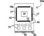
用于实现本发明的已知模式是集成照相机模块。本发明的集成照相机模块在图1的侧视图中示出,并且用总的附图标记10标示。集成照相机模块10具有照相机芯片12,其本身与诸如现在使用的或未来研制的其它照相机芯片并无不同。本领域的普通技术人员知道,照相机芯片12具有传感器阵列区域14,并且还包括传感器阵列区域14拍摄图像所需或希望具有的许多其它元件(定时装置等)。在图1的示例中,照相机模块12连接(在下文中将更详细地讨论)到印刷线路板(“PCB”)16上。照相机芯片12用多根(在图1的图中仅仅可看见两根)焊线连线17电连接至PCB 16。A known mode for implementing the invention is an integrated camera module. The integrated camera module of the present invention is shown in side view in FIG. 1 and is designated by the
PCB 16上面具有多个无源元件18,其与照相机芯片12上的元件结合,构成集成照相机模块10的内部电路。可选择地,在某些应用中PCB 16具有多个(为了清楚起见,在图1的图示中仅仅示出几个)底部接触焊盘20,用于将集成照相机模块10电连接至外部元件(未示出),例如操作按钮、可选闪光电路、外部数字存储器、外部控制电路等。上述元件一起构成PCB组件22,该组件在许多方面与目前类似的照相机模块中使用的那些元件并无显著不同。There are a plurality of
根据本发明,透镜组件24用模制件26相对于PCB组件22定位,并且用粘接剂28固定在适当的位置。模制件26通过PCB组件上的模制材料形成,如在下文中更详细地讨论。模制件26具有足够精确的尺寸公差,使得当透镜组件24位于模制件26的凹陷区29(图2)内时,如图1的示例所示,间隙30适于透镜组件24相对于PCB组件22的聚焦。透镜组件24和传感器阵列区14之间的最佳距离取决于使用的具体透镜的几何形状和材料。在图1的视图中可以看出,间隙30的高度是透镜组件24在Z维度32上的位置的函数,该位置在下文中将更详细地讨论。In accordance with the present invention,
应该注意,透镜组件24并不意味着描述任何具体的透镜设计,而是出于图解的目的代表性地示出。根据具体的设计,透镜组件24可以由单片材料形成,可以包括一个或多个安装在支座(例如,图10)中的透镜,或可以包括另外的光学元件。It should be noted that
保护盖33安装在传感器阵列区14上面,以防止传感器阵列区14在制造和组装过程中受损伤。优选地,保护盖33由坚固的不旋光材料形成。在一个具体实施例中,保护盖是玻璃盖片,其可以在模制件26形成之前或形成过程中安装在传感器阵列区14上。A
图2是图1的集成照相机模块10在透镜组件24定位于其上之前的示意俯视平面图。从图2的视图中可以看出,透镜组件24(图1)在X维度34和Y维度36上的位置通过凹陷区29在模制件26中的位置和公差来实现。在模制件26中设有小孔38,通过小孔38可以看见传感器阵列区14。2 is a schematic top plan view of
图3是PCB组件22a的另一示例的俯视平面图。在图3的示例中,可以看出照相机芯片12固定(在这个示例中用粘接剂)到可替换PCB 16a上。非常多的连接线17连接至可替换PCB 16a上的相同数量的多个连接焊盘42,用于形成可替换PCB 16a与照相机芯片12之间的电连接。可替换PCB 16a还具有多个连接接头40,用于将可替换PCB组件22a与外部电路电连接。与图1的示例不同,在图3的示例中,所有无源元件18位于照相机芯片12的一侧。FIG. 3 is a top plan view of another example of a
图4是柔性电路44的仰视平面图。柔性电路44上具有多个连接接头40,用于与可替换PCB组件上的相同数量的多个连接接头40配合。而且,柔性电路44具有多个边缘连接器焊盘46,用于与外部电路的连接。FIG. 4 is a bottom plan view of
图5是图3的可替换PCB组件22a固定到图4的柔性电路44上得到的组装的柔性电路组件48的俯视平面图。应该注意,可替换PCB组件22a可以直接连接至刚性电路板等,而不连接至柔性电路44。然而,在有些应用中,柔性电路44在设置可替换PCB组件22a时可以有更大的自由度。此外,如果必要或需要,在柔性电路44上可以包括附加电路。柔性电路44包括迹线(trace)(未示出),用于按要求提供连接接头40和边缘连接焊盘46以及如上所述的可选附加电路之间的电连接。5 is a top plan view of assembled
在图5的视图中可以看出,在柔性电路组件48中,可替换PCB组件22a在热把(hot bar)连接点50处连接至柔性电路44,使得连接接头40(在图5的视图中看不见)按要求配合。本领域的普通技术人员熟悉热把连接法,上述元件正是通过该方法在热把连接点50处连接的。As can be seen in the view of FIG. 5, in the
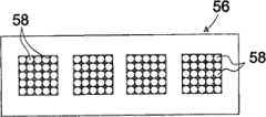
图6是衬底条52的俯视轮廓平面图。衬底条52具有包括在其中的多个(在所示的示例中为100个)单独的PCB 16a。衬底条52还具有多个(在本示例中为18)对准孔54,用于在一个或多个定位夹具(未示出)中对准衬底条52。FIG. 6 is a top profile plan view of
图7是诸如可以用于实现本发明的模箍(mold chase)56的俯视示意平面图。模箍56由金属,诸如不锈钢构成。模箍适于将多个(在本示例中为100)模制插入件58固定在适当位置。当模箍56在衬底条52上对准时,模制插入件58定位成在衬底条52(图6)的每一个PCB 16a上正确对准一个模制插入件58。Figure 7 is a top schematic plan view of a
图8是对准于可替换PCB组件22a之一上的一个模制插入件58的示意侧视图。如在下文中更详细地讨论的,除了这里所注意到的,在衬底条52被分成单独的可替换PCB组件22a之前,在衬底条52上构成可替换PCB组件22a。在图8的视图中可以看出,模制插入件58涂敷有顺从的、无粘着力的材料层59,以防止损伤下面的传感器12和/或防止模制件26的材料粘接到模制插入件58上。如本领域的普通技术人员已知的,用于涂层的具体材料59取决于模制件26的具体成分;而且在有些应用中,涂敷材料59可省略。因此,涂敷材料59不视为是本发明的必要元素。应该注意,模制过程本身对本发明来说不是特殊的。模制技术是本领域的公知常识,本领域的普通技术人员熟悉正确形成在此讨论的模制件26和等同物所需的细节。Figure 8 is a schematic side view of a molded
图9是衬底条52的一个示例的俯视平面图,该衬底条在其上的适当位置处具有保护带,用于在本发明的一些组装过程中保护PCB组件16a(在图9的视图中看不见)。以下将就本发明的用于生产集成照相机模块10的方法更详细地讨论保护带60的使用。FIG. 9 is a top plan view of one example of a
图10是根据本发明的集成照相机模块10a的另一实施例。在图10的视图中,可以看出可替换透镜组件24a具有塑料透镜座62、第一透镜64和第二透镜66。本领域的普通技术人员认为,集成照相机模块10a一般需要两个透镜。因此,诸如图10的视图所示的布置发明者认为是最佳的。然而,发明也可以仅利用一个透镜来实施。第一透镜64与第二透镜66之间的距离通过透镜座62的结构来固定。第一透镜64和照相机芯片12之间的距离如下文中讨论的那样设定。在图10的示例中,粘接剂槽70围绕模制件26的周边设置,用于接收粘结剂28,以将透镜组件24a固定在模制件26内的适当位置上。FIG. 10 is another embodiment of an
图11是图示本发明照相机模块构造方法100的示例的流程图。在这个实施例中,同时构造多个照相机模块。首先,在“照相机芯片安装”操作102中,一个或多个照相机芯片12分别安装到一个或多个PCB 16a上(图6)。接下来,在“透镜座二次模制”操作103中,在每个照相机芯片12上模制透镜座26。然后,在“装置分离”操作104中,PCB 16a彼此分离(例如,锯开)。接下来,在“透镜安装”操作105中,透镜座62安装到每个透镜座模制件26(图10)中。最后,在“封装”操作106中,所完成的集成照相机模块10a被封装,以便运输到微型照相机制造商、电话照相机制造商等那里,或如上所述连接至柔性电路44上。FIG. 11 is a flowchart illustrating an example of a camera
图12是概括用于执行方法100的照相机芯片安装操作102的一个具体方法107的流程图。首先,在“保护盖定位”操作108中,保护盖33被定位在照相机芯片12上(图10)。可选地,保护盖33可以在透镜座二次模制操作103过程中定位,或者在照相机芯片安装操作102中的另一位置被定位,或者省略。接下来,在“焊锡膏印刷”操作110中,焊锡膏迹线被印刷在衬底条52的各个PCB 16a上。在“无源连接”操作112中,无源元件18被放置在PCB 16a上。在“回流”操作114中,衬底条52经过回流焊操作,在“清洁器”操作116中,衬底条52在回流焊处理114之后经过传统的清洁处理。FIG. 12 is a flowchart outlining one
在“管芯接合”操作118中,照相机芯片12接合至(在这个示例中用粘结剂)相应的PCB 16a。在“炉内固化”操作120中,之前操作中所施加的粘结剂在炉子中被固化。在“等离子体清洁”操作122中,利用惰性气体对接合了引线(在随后的操作中)的表面进行蚀刻。在“线接合”操作124中,连接线17利用热接合方法接合。在第二次“等离子体清洁”操作126中,再次清洁PCB 16a。In a "die bonding"
图13是概括用于执行方法100中的透镜座二次模制操作103的一种具体方法127的流程图。在保护盖定位操作128中,保护盖33被定位在照相机芯片12上。应该注意,如果作为前面处理的一部分保护盖33已经被安装,或如果不希望采用保护盖,则这个步骤不是必需的。然后,在“二次模制”操作129中,模箍56放在衬底条52上,并如前所述形成模制件26。除了在此已经描述的功能之外,模制件26还起到将保护盖33固定在适当位置的作用,实质上密封了照相机芯片12的传感器阵列区14。模制件26利用本领域普通技术人员已知的普通常规“二次模制”技术形成。在模制操作之后,模型可露出照相机芯片12的传感器阵列区14。最后,在“O/M固化”操作130中,模制件26被快速地热固化。FIG. 13 is a flowchart outlining one particular method 127 for performing the lens
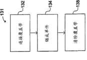
图14是概括用于执行图11的装置分离操作104的一个具体方法131的流程图。首先,在“连接覆盖带”操作132中,保护带60被设置在所有PCB16a(如图9所示)上。然后,在“锯成单件”操作134中,个体的PCB 16a被锯开。锯割是穿过保护盖60进行的,使得所获得的产品是多个个体的PCB组件22a,每个PCB组件22a上仍然保持着保护带60的一个相应的部分。保护带60是通常可买到的商品,用于在焊接等过程中保护元件。最后,在“清除覆盖带”操作138中,从每个PCB组件22a清除保护带60的小块。FIG. 14 is a flowchart outlining one
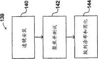
图15是概括用于执行方法100中的透镜安装操作105的一个具体方法139的流程图。在“透镜安装”操作140中,在每个模制件26中插入一个透镜组件24a(图10)。在“聚焦和测试”操作142中,透镜组件24a上下移动,(沿图1的Z轴32),以优选透镜组件24a相对照相机芯片12的传感器阵列区14的焦距。一般通过常规的自动测试设备确定正确的焦距。应该注意,发明者认为,通过参照“二次模制”操作过程128中模箍56相对于照相机芯片12的位置,这个操作可能在未来可以取消。最后,在“胶剂涂布和固化”操作144中,如上所述涂布紫外线固化粘接剂28,然后利用超紫外光将其固化。FIG. 15 is a flowchart outlining one
本发明可以做出各种变型,而不改变它的价值或范围。例如,对于在此讨论的示例中图示和描述的元件尺寸、形状和数量可以根据具体应用的需要和便利性而各自改变或全部改变。Various modifications may be made to the invention without altering its value or scope. For example, the size, shape and number of elements illustrated and described in the examples discussed herein may be varied individually or in total according to the needs and convenience of a particular application.
类似地,其它衬底材料,诸如陶瓷,可以用于代替在此描述的PCB 16。Similarly, other substrate materials, such as ceramics, may be used in place of the
另一种变型是用由例如透明塑料、玻璃、或一些其它的光学上可接受的材料制成的光学透明间隔物代替这里所描述的充有空气的间隙30。设置抵靠于照相机芯片12和透镜24两者之上的间隔物可以使得在透镜安装操作过程中不需要对透镜进行聚焦。同样,第二透镜,诸如变焦透镜组件等,可以装配到已经机械对中的透镜组件24或24a上。间隔物同时起到保护盖的作用,从而不需要提供独立的保护盖。Another variation is to replace the air-filled
尽管发明者目前认为用粘接剂将透镜组件24、24a安装到模制件26等中是目前最可靠的方法,但透镜组件24、24a可以用其它的机械装置(诸如机械夹具等)固接到PCB 16、16a与照相机芯片12上,这落入本发明范围之内。The
对方法的显而易见的改变可以包括在“锯成单件”操作134之前将透镜组件24a安装到模制件26中。当然,这需要对方法做出一些其它变化,以保证传感器阵列区14在“锯成单件”操作134等中受到保护。An obvious variation to the method may include installing the
在本发明可以容易地添加附加的元件和/或部件。一个可能的示例是在模制件26上设置玻璃盖。这样的盖可以用于几个目的。它可以在存储、运输和操作过程中保护传感器阵列区14,或者它可以起到使装置可以利用“拾放”机器(“pick-and-place”machine)被提升的作用,并且它可以在回流焊操作过程中保护传感器阵列区14。Additional elements and/or components can be readily added to the present invention. One possible example is to provide a glass cover on the
上述所有的示例仅仅是本发明的可行实施例的一些示例。本领域的普通技术人员很容易看到,在不背离本发明精神和范围的情况下,可以作出许多其它的变型和变化。因此,这里的公开并不是限制性的,而所附权利要求将被视为覆盖本发明的整个范围。All of the above examples are only some examples of possible embodiments of the invention. It will be readily apparent to those skilled in the art that many other modifications and changes can be made without departing from the spirit and scope of the invention. Accordingly, the disclosure herein is not intended to be limiting and the appended claims are to be regarded as covering the full scope of the invention.
工业实用性Industrial Applicability
本发明的集成照相机模块10、10a打算广泛应用于在非常小的装置,诸如小型数字照相机、手机等中,用于拍摄视频图像。该装置和方法适于各种应用,包括利用从VGA分辨率至1.3兆甚至更高像素范围的传感器模块的应用。在此描述的方法和装置在模制材料方面并不昂贵,而且加工成本低于利用传统方法的透镜座连接的成本。这主要是因为模制处理是在其上具有许多集成照相机模块10的整个面板上同时进行的,而不是一次一个地连接透镜。同时,模制复合结构的成本低于模制原先连接透镜的单个透镜座零件的成本。The
根据本发明,集成照相机模块10的最终组件更更加牢固,而且就X和Y位置而言将更加精确。这是通过确保利用衬底上的相同位置基准特征来控制传感器管芯和二次模制插入件位置而实现的。目前的方法涉及使用导向销和用于设置透镜座的其它装置。与具有更高尺寸精度和更稳定尺寸的模具相比,这些情况固有地导致公差更大。According to the present invention, the final assembly of the
如上所述,Z维度上的精度可以参照照相机芯片12表面本身来实现,所述表面是用于照相机聚焦的主要参照物。可以预期,将来在绝大多数情况下不需要进行主动对准。同样,不需要将透镜组件旋转到螺纹座中进行对准的事实本质上使透镜位置更稳定。As mentioned above, precision in the Z dimension can be achieved with reference to the
另外可以预期到,本发明所需的元件的数量减少,这可以节约额外成本。It is also contemplated that the number of components required by the invention is reduced, which leads to additional cost savings.
由于本发明的集成照相机模块10、10a可以方便地生产并与现有的照相机系统设计构造以及其它可能设想出的构造集成,并且由于本发明具有上述优点,所以其有望很快地在工业上被接受。由于这些和其它原因,可以预见,本发明的用途和工业应用将范围广泛并且持续时间长久。Since the
Claims (26)
Translated fromChineseApplications Claiming Priority (2)
| Application Number | Priority Date | Filing Date | Title |
|---|---|---|---|
| US10/784,102US7872686B2 (en) | 2004-02-20 | 2004-02-20 | Integrated lens and chip assembly for a digital camera |
| US10/784,102 | 2004-02-20 |
Related Parent Applications (1)
| Application Number | Title | Priority Date | Filing Date |
|---|---|---|---|
| CNA2005800089902ADivisionCN101124813A (en) | 2004-02-20 | 2005-02-18 | Integrated lens and chip assembly for digital camera |
Publications (2)
| Publication Number | Publication Date |
|---|---|
| CN101656218Atrue CN101656218A (en) | 2010-02-24 |
| CN101656218B CN101656218B (en) | 2012-02-08 |
Family
ID=34861402
Family Applications (2)
| Application Number | Title | Priority Date | Filing Date |
|---|---|---|---|
| CN2009101706321AExpired - LifetimeCN101656218B (en) | 2004-02-20 | 2005-02-18 | Method for producing camera module and corresponding substrate |
| CNA2005800089902APendingCN101124813A (en) | 2004-02-20 | 2005-02-18 | Integrated lens and chip assembly for digital camera |
Family Applications After (1)
| Application Number | Title | Priority Date | Filing Date |
|---|---|---|---|
| CNA2005800089902APendingCN101124813A (en) | 2004-02-20 | 2005-02-18 | Integrated lens and chip assembly for digital camera |
Country Status (7)
| Country | Link |
|---|---|
| US (2) | US7872686B2 (en) |
| EP (2) | EP1726157A4 (en) |
| JP (1) | JP2007523568A (en) |
| CN (2) | CN101656218B (en) |
| CA (1) | CA2556477A1 (en) |
| TW (1) | TWI258052B (en) |
| WO (1) | WO2005081853A2 (en) |
Cited By (1)
| Publication number | Priority date | Publication date | Assignee | Title |
|---|---|---|---|---|
| CN104916008A (en)* | 2015-06-26 | 2015-09-16 | 深圳市安视达电子科技有限公司 | Automobile data recorder |
Families Citing this family (55)
| Publication number | Priority date | Publication date | Assignee | Title |
|---|---|---|---|---|
| JP2005101711A (en)* | 2003-09-22 | 2005-04-14 | Renesas Technology Corp | Solid-state imaging device and manufacturing method thereof |
| US7872686B2 (en)* | 2004-02-20 | 2011-01-18 | Flextronics International Usa, Inc. | Integrated lens and chip assembly for a digital camera |
| US7796187B2 (en)* | 2004-02-20 | 2010-09-14 | Flextronics Ap Llc | Wafer based camera module and method of manufacture |
| JP2005284147A (en)* | 2004-03-30 | 2005-10-13 | Fuji Photo Film Co Ltd | Imaging device |
| US20050264690A1 (en)* | 2004-05-28 | 2005-12-01 | Tekom Technologies, Inc. | Image sensor |
| EP1769719A4 (en)* | 2004-07-05 | 2009-10-21 | Olympus Medical Systems Corp | ELECTRONIC ENDOSCOPE |
| KR100677380B1 (en)* | 2004-11-05 | 2007-02-02 | 엘지전자 주식회사 | Camera lens protector for slide type mobile terminal |
| JP4852535B2 (en)* | 2005-04-01 | 2012-01-11 | パナソニック株式会社 | Imaging device |
| US7288757B2 (en)* | 2005-09-01 | 2007-10-30 | Micron Technology, Inc. | Microelectronic imaging devices and associated methods for attaching transmissive elements |
| US7531773B2 (en) | 2005-09-08 | 2009-05-12 | Flextronics Ap, Llc | Auto-focus and zoom module having a lead screw with its rotation results in translation of an optics group |
| US7469100B2 (en) | 2005-10-03 | 2008-12-23 | Flextronics Ap Llc | Micro camera module with discrete manual focal positions |
| DE102006013164A1 (en)* | 2006-03-22 | 2007-09-27 | Robert Bosch Gmbh | Method for mounting a camera module and camera module |
| US20070236591A1 (en)* | 2006-04-11 | 2007-10-11 | Tam Samuel W | Method for mounting protective covers over image capture devices and devices manufactured thereby |
| US8092102B2 (en)* | 2006-05-31 | 2012-01-10 | Flextronics Ap Llc | Camera module with premolded lens housing and method of manufacture |
| DE102006043323A1 (en)* | 2006-09-15 | 2008-03-27 | Robert Bosch Gmbh | Pressure sensor for side impact sensing and method of forming a surface of a protective material for a pressure sensor |
| US7983556B2 (en)* | 2006-11-03 | 2011-07-19 | Flextronics Ap Llc | Camera module with contamination reduction feature |
| US8456560B2 (en)* | 2007-01-26 | 2013-06-04 | Digitaloptics Corporation | Wafer level camera module and method of manufacture |
| CA2685080A1 (en) | 2007-04-24 | 2008-11-06 | Flextronics Ap Llc | Small form factor modules using wafer level optics with bottom cavity and flip-chip assembly |
| US8488046B2 (en)* | 2007-12-27 | 2013-07-16 | Digitaloptics Corporation | Configurable tele wide module |
| US9118825B2 (en)* | 2008-02-22 | 2015-08-25 | Nan Chang O-Film Optoelectronics Technology Ltd. | Attachment of wafer level optics |
| WO2010091347A1 (en)* | 2009-02-06 | 2010-08-12 | Magna Electronics Inc. | Improvements to camera for vehicle |
| JP5487842B2 (en)* | 2009-06-23 | 2014-05-14 | ソニー株式会社 | Solid-state imaging device |
| US8265487B2 (en)* | 2009-07-29 | 2012-09-11 | Avago Technologies Fiber Ip (Singapore) Pte. Ltd. | Half-duplex, single-fiber (S-F) optical transceiver module and method |
| US9419032B2 (en)* | 2009-08-14 | 2016-08-16 | Nanchang O-Film Optoelectronics Technology Ltd | Wafer level camera module with molded housing and method of manufacturing |
| US8760571B2 (en) | 2009-09-21 | 2014-06-24 | Microsoft Corporation | Alignment of lens and image sensor |
| US10782187B2 (en)* | 2010-07-08 | 2020-09-22 | Cvg Management Corporation | Infrared temperature measurement and stabilization thereof |
| KR20120079551A (en)* | 2011-01-05 | 2012-07-13 | 엘지이노텍 주식회사 | Focus free camera module |
| US8545114B2 (en) | 2011-03-11 | 2013-10-01 | Digitaloptics Corporation | Auto focus-zoom actuator or camera module contamination reduction feature with integrated protective membrane |
| US9178093B2 (en) | 2011-07-06 | 2015-11-03 | Flextronics Ap, Llc | Solar cell module on molded lead-frame and method of manufacture |
| WO2013079705A1 (en)* | 2011-11-30 | 2013-06-06 | Anteryon International Bv | Apparatus and method |
| JP2014138119A (en)* | 2013-01-17 | 2014-07-28 | Sony Corp | Semiconductor device and semiconductor device manufacturing method |
| JP5958364B2 (en)* | 2013-01-28 | 2016-07-27 | 日立金属株式会社 | Optical module |
| CN104376616A (en)* | 2013-08-16 | 2015-02-25 | 深圳富泰宏精密工业有限公司 | Automobile data recorder |
| TWI650016B (en) | 2013-08-22 | 2019-02-01 | 新力股份有限公司 | Imaging device, manufacturing method and electronic device |
| US9258467B2 (en)* | 2013-11-19 | 2016-02-09 | Stmicroelectronics Pte Ltd. | Camera module |
| US9467606B2 (en)* | 2014-06-10 | 2016-10-11 | Omnivision Technologies, Inc. | Wafer level stepped sensor holder |
| US10447900B2 (en)* | 2015-08-06 | 2019-10-15 | Apple Inc. | Camera module design with lead frame and plastic moulding |
| KR102465474B1 (en)* | 2016-02-18 | 2022-11-09 | 닝보 써니 오포테크 코., 엘티디. | Integral packaging process-based camera module, integral base component of same, and manufacturing method therefor |
| KR102335306B1 (en)* | 2016-03-12 | 2021-12-03 | 닝보 써니 오포테크 코., 엘티디. | Array Imaging Module and Molded Photensitive Assembly and Manufacturing Method Thereof for Electronic Device |
| US10750071B2 (en)* | 2016-03-12 | 2020-08-18 | Ningbo Sunny Opotech Co., Ltd. | Camera module with lens array arrangement, circuit board assembly, and image sensor and manufacturing method thereof |
| EP3446338A4 (en)* | 2016-03-23 | 2019-06-05 | AMS Sensors Singapore Pte. Ltd. | Optoelectronic module assembly and manufacturing method |
| CN107466160B (en) | 2016-06-06 | 2022-04-29 | 宁波舜宇光电信息有限公司 | Equipment and method for manufacturing molded circuit board of camera module |
| CN107466159B (en) | 2016-06-06 | 2022-07-19 | 宁波舜宇光电信息有限公司 | Molded circuit board of camera module and its manufacturing equipment and manufacturing method |
| KR101785458B1 (en)* | 2016-06-07 | 2017-10-16 | 엘지전자 주식회사 | Camera module and mobile terminal having the same |
| KR102405359B1 (en)* | 2017-02-08 | 2022-06-07 | 닝보 써니 오포테크 코., 엘티디. | Photographing module and mold photosensitive assembly and manufacturing method thereof, and electronic device |
| CN108461510A (en)* | 2017-02-22 | 2018-08-28 | 深圳市中兴微电子技术有限公司 | A kind of camera module and preparation method thereof |
| CN106998417A (en)* | 2017-03-24 | 2017-08-01 | 谢超 | Miniature video camera module manufacture craft |
| CN110914753A (en)* | 2017-07-31 | 2020-03-24 | 日本电产株式会社 | Light-blocking blade, blade drive device, and imaging device |
| CN110945424A (en)* | 2017-07-31 | 2020-03-31 | 日本电产株式会社 | Light-blocking blade, blade drive device, and imaging device |
| WO2019026449A1 (en)* | 2017-07-31 | 2019-02-07 | 日本電産株式会社 | Light-shielding blade, blade drive device, and imaging device |
| CN110475049B (en)* | 2018-05-11 | 2022-03-15 | 三星电机株式会社 | Camera module and method of manufacturing the same |
| CN110611754A (en)* | 2018-06-15 | 2019-12-24 | 三赢科技(深圳)有限公司 | camera module |
| JP7641740B2 (en) | 2018-07-06 | 2025-03-07 | 浜松ホトニクス株式会社 | Spectroscopic module and method for manufacturing the same |
| US20210321025A1 (en)* | 2018-08-21 | 2021-10-14 | Ningbo Sunny Opotech Co., Ltd. | Camera module and molded photosensitive assembly and manufacturing methods thereof, and electronic device |
| US11094858B2 (en)* | 2019-08-01 | 2021-08-17 | Advanced Semiconductor Engineering, Inc. | Tape, encapsulating process and optical device |
Family Cites Families (54)
| Publication number | Priority date | Publication date | Assignee | Title |
|---|---|---|---|---|
| JPH0724287B2 (en)* | 1987-02-12 | 1995-03-15 | 三菱電機株式会社 | Semiconductor device having light transmitting window and method of manufacturing the same |
| US5617131A (en)* | 1993-10-28 | 1997-04-01 | Kyocera Corporation | Image device having a spacer with image arrays disposed in holes thereof |
| JP3247384B2 (en)* | 1994-03-18 | 2002-01-15 | 日立化成工業株式会社 | Semiconductor package manufacturing method and semiconductor package |
| KR20040004472A (en)* | 1995-05-31 | 2004-01-13 | 소니 가부시끼 가이샤 | Image pickup apparatus, fabrication method thereof, image pickup adaptor apparatus, signal processing apparatus, signal processing method thereof, information processing apparatus, and information processing method |
| NL1003315C2 (en) | 1996-06-11 | 1997-12-17 | Europ Semiconductor Assembly E | Method for encapsulating an integrated semiconductor circuit. |
| JPH10321827A (en)* | 1997-05-16 | 1998-12-04 | Sony Corp | Imaging device and camera |
| JP2000241696A (en)* | 1999-02-17 | 2000-09-08 | Canon Inc | How to hold and mount the optical sensor package |
| US6483101B1 (en)* | 1999-12-08 | 2002-11-19 | Amkor Technology, Inc. | Molded image sensor package having lens holder |
| JP2001188155A (en) | 1999-12-28 | 2001-07-10 | Kuurii Components Kk | Image sensor fixing means |
| JP3651580B2 (en) | 2000-04-07 | 2005-05-25 | 三菱電機株式会社 | Imaging apparatus and manufacturing method thereof |
| US6384397B1 (en)* | 2000-05-10 | 2002-05-07 | National Semiconductor Corporation | Low cost die sized module for imaging application having a lens housing assembly |
| EP1180718A1 (en)* | 2000-08-11 | 2002-02-20 | EM Microelectronic-Marin SA | Apparatus for taking images of small dimensions, particularly still or motion picture camera |
| JP3725012B2 (en)* | 2000-08-17 | 2005-12-07 | シャープ株式会社 | Manufacturing method of lens-integrated solid-state imaging device |
| JP3887162B2 (en)* | 2000-10-19 | 2007-02-28 | 富士通株式会社 | Imaging semiconductor device |
| US6686588B1 (en)* | 2001-01-16 | 2004-02-03 | Amkor Technology, Inc. | Optical module with lens integral holder |
| JP3821652B2 (en) | 2001-02-26 | 2006-09-13 | 三菱電機株式会社 | Imaging device |
| DE10109787A1 (en)* | 2001-02-28 | 2002-10-02 | Infineon Technologies Ag | Digital camera with a light-sensitive sensor |
| US6798031B2 (en)* | 2001-02-28 | 2004-09-28 | Fujitsu Limited | Semiconductor device and method for making the same |
| US20040012698A1 (en)* | 2001-03-05 | 2004-01-22 | Yasuo Suda | Image pickup model and image pickup device |
| JP2003032525A (en)* | 2001-05-09 | 2003-01-31 | Seiko Precision Inc | Solid state imaging apparatus |
| JP2003060948A (en)* | 2001-06-05 | 2003-02-28 | Seiko Precision Inc | Solid-state photographing apparatus |
| US6734419B1 (en)* | 2001-06-28 | 2004-05-11 | Amkor Technology, Inc. | Method for forming an image sensor package with vision die in lens housing |
| CN1249991C (en)* | 2001-08-07 | 2006-04-05 | 日立麦克赛尔株式会社 | Camera module |
| JP4647851B2 (en) | 2001-08-07 | 2011-03-09 | 日立マクセル株式会社 | The camera module |
| JP2003078077A (en) | 2001-09-05 | 2003-03-14 | Sanyo Electric Co Ltd | The camera module |
| JP3887208B2 (en) | 2001-10-29 | 2007-02-28 | 富士通株式会社 | Camera module and manufacturing method thereof |
| JP4143304B2 (en) | 2002-01-24 | 2008-09-03 | 富士通株式会社 | Manufacturing method of camera module |
| JP2003333437A (en)* | 2002-05-13 | 2003-11-21 | Rohm Co Ltd | Image sensor module and manufacturing method thereof |
| US7304362B2 (en)* | 2002-05-20 | 2007-12-04 | Stmicroelectronics, Inc. | Molded integrated circuit package with exposed active area |
| US7583309B2 (en)* | 2002-06-28 | 2009-09-01 | Kyocera Coproration | Imaging device package camera module and camera module producing method |
| AU2003256383A1 (en)* | 2002-07-03 | 2004-01-23 | Concord Camera Corp. | Compact zoom lens barrel and system |
| US7564496B2 (en)* | 2002-09-17 | 2009-07-21 | Anteryon B.V. | Camera device, method of manufacturing a camera device, wafer scale package |
| JP2004194223A (en) | 2002-12-13 | 2004-07-08 | Konica Minolta Holdings Inc | Imaging device and mobile terminal |
| JP2004200965A (en) | 2002-12-18 | 2004-07-15 | Sanyo Electric Co Ltd | Camera module and manufacturing method thereof |
| JP2004296453A (en)* | 2003-02-06 | 2004-10-21 | Sharp Corp | Solid-state imaging device, semiconductor wafer, module for optical device, method for manufacturing solid-state imaging device, and method for manufacturing module for optical device |
| US6741405B1 (en)* | 2003-03-27 | 2004-05-25 | Exquisite Optical Technology Co., Ltd | Hood for a digital image collecting lens |
| US7122787B2 (en)* | 2003-05-09 | 2006-10-17 | Matsushita Electric Industrial Co., Ltd. | Imaging apparatus with three dimensional circuit board |
| US7619683B2 (en)* | 2003-08-29 | 2009-11-17 | Aptina Imaging Corporation | Apparatus including a dual camera module and method of using the same |
| US7199438B2 (en)* | 2003-09-23 | 2007-04-03 | Advanced Semiconductor Engineering, Inc. | Overmolded optical package |
| KR100541654B1 (en)* | 2003-12-02 | 2006-01-12 | 삼성전자주식회사 | Wiring board and semiconductor device for solid-state imaging using same |
| US7091571B1 (en)* | 2003-12-11 | 2006-08-15 | Amkor Technology, Inc. | Image sensor package and method for manufacture thereof |
| JP2005210628A (en) | 2004-01-26 | 2005-08-04 | Mitsui Chemicals Inc | Substrate for mounting semiconductor for imaging device, and imaging device |
| US7872686B2 (en) | 2004-02-20 | 2011-01-18 | Flextronics International Usa, Inc. | Integrated lens and chip assembly for a digital camera |
| US7796187B2 (en)* | 2004-02-20 | 2010-09-14 | Flextronics Ap Llc | Wafer based camera module and method of manufacture |
| JP4446773B2 (en)* | 2004-03-26 | 2010-04-07 | 富士フイルム株式会社 | Imaging device |
| US7061106B2 (en)* | 2004-04-28 | 2006-06-13 | Advanced Chip Engineering Technology Inc. | Structure of image sensor module and a method for manufacturing of wafer level package |
| JP5252770B2 (en)* | 2004-06-10 | 2013-07-31 | 三星電子株式会社 | Image sensor package assembly method |
| JP2005352314A (en)* | 2004-06-11 | 2005-12-22 | Canon Inc | Imaging apparatus and electronic apparatus |
| KR100652375B1 (en)* | 2004-06-29 | 2006-12-01 | 삼성전자주식회사 | Image sensor module structure including wire bonding package and manufacturing method thereof |
| KR100674911B1 (en)* | 2004-08-06 | 2007-01-26 | 삼성전자주식회사 | Image sensor camera module and its manufacturing method |
| JP2006053232A (en) | 2004-08-10 | 2006-02-23 | Sony Corp | Electronic imaging device |
| US20070058069A1 (en)* | 2005-09-14 | 2007-03-15 | Po-Hung Chen | Packaging structure of a light sensation module |
| KR100770684B1 (en)* | 2006-05-18 | 2007-10-29 | 삼성전기주식회사 | Camera module package |
| US8092102B2 (en)* | 2006-05-31 | 2012-01-10 | Flextronics Ap Llc | Camera module with premolded lens housing and method of manufacture |
- 2004
- 2004-02-20USUS10/784,102patent/US7872686B2/ennot_activeExpired - Fee Related
- 2005
- 2005-02-16TWTW094104486Apatent/TWI258052B/ennot_activeIP Right Cessation
- 2005-02-18EPEP05713765Apatent/EP1726157A4/ennot_activeWithdrawn
- 2005-02-18CNCN2009101706321Apatent/CN101656218B/ennot_activeExpired - Lifetime
- 2005-02-18EPEP10177430Apatent/EP2265000A1/ennot_activeWithdrawn
- 2005-02-18CNCNA2005800089902Apatent/CN101124813A/enactivePending
- 2005-02-18WOPCT/US2005/005139patent/WO2005081853A2/enactiveApplication Filing
- 2005-02-18JPJP2006554218Apatent/JP2007523568A/enactivePending
- 2005-02-18CACA002556477Apatent/CA2556477A1/ennot_activeAbandoned
- 2011
- 2011-01-18USUS12/930,822patent/US8477239B2/ennot_activeExpired - Fee Related
Cited By (1)
| Publication number | Priority date | Publication date | Assignee | Title |
|---|---|---|---|---|
| CN104916008A (en)* | 2015-06-26 | 2015-09-16 | 深圳市安视达电子科技有限公司 | Automobile data recorder |
Also Published As
| Publication number | Publication date |
|---|---|
| US8477239B2 (en) | 2013-07-02 |
| US20050185088A1 (en) | 2005-08-25 |
| EP2265000A1 (en) | 2010-12-22 |
| US7872686B2 (en) | 2011-01-18 |
| CA2556477A1 (en) | 2005-09-09 |
| CN101656218B (en) | 2012-02-08 |
| EP1726157A4 (en) | 2009-01-07 |
| CN101124813A (en) | 2008-02-13 |
| TWI258052B (en) | 2006-07-11 |
| JP2007523568A (en) | 2007-08-16 |
| TW200530731A (en) | 2005-09-16 |
| WO2005081853A2 (en) | 2005-09-09 |
| EP1726157A2 (en) | 2006-11-29 |
| WO2005081853A3 (en) | 2007-08-02 |
| US20110115974A1 (en) | 2011-05-19 |
Similar Documents
| Publication | Publication Date | Title |
|---|---|---|
| CN101656218B (en) | Method for producing camera module and corresponding substrate | |
| US7796187B2 (en) | Wafer based camera module and method of manufacture | |
| JP7071926B2 (en) | Camera module and its photosensitive parts and their manufacturing method | |
| CN102577644B (en) | Wafer-level camera module with molded housing and manufacturing method | |
| US7964945B2 (en) | Glass cap molding package, manufacturing method thereof and camera module | |
| KR100915134B1 (en) | Image sensor camera module and method of manufacturing the same | |
| CN101432759B (en) | System and method for mounting an image record device on a flexible substrate | |
| US20110299848A1 (en) | Camera Module with Premolded Lens Housing and Method of Manufacture | |
| JP2013516656A (en) | Camera module with molded tape flip chip imaging device mounting and manufacturing method | |
| US7619684B2 (en) | Camera module, manufacturing method of camera module, electronic apparatus, and manufacturing method of electronic apparatus | |
| WO2014075462A1 (en) | Bracket-type image sensing module and manufacturing method therefor and multi-camera apparatus | |
| KR20120029208A (en) | Filter package for camera module and camera module | |
| KR100613419B1 (en) | Image sensor module and its manufacturing method | |
| KR100917026B1 (en) | Glass cap molding package and manufacturing method thereof, and camera module | |
| KR100795601B1 (en) | Camera module and manufacturing method thereof | |
| KR100927423B1 (en) | Glass cap molding package and manufacturing method thereof, and camera module | |
| JP2007273696A (en) | Image sensing module and method of manufacturing the same | |
| KR100814922B1 (en) | Camera module | |
| KR20130091379A (en) | Auto focus camera module by power line incert molding and method of manufacturing the same | |
| JP2005259993A (en) | Module product and its manufacturing method |
Legal Events
| Date | Code | Title | Description |
|---|---|---|---|
| C06 | Publication | ||
| PB01 | Publication | ||
| C10 | Entry into substantive examination | ||
| SE01 | Entry into force of request for substantive examination | ||
| C14 | Grant of patent or utility model | ||
| GR01 | Patent grant | ||
| ASS | Succession or assignment of patent right | Owner name:DIGITAL OPTICS CORP. Free format text:FORMER OWNER: FLEXTRONICS INTERNAT USA INC. Effective date:20140417 | |
| C41 | Transfer of patent application or patent right or utility model | ||
| TR01 | Transfer of patent right | Effective date of registration:20140417 Address after:California, USA Patentee after:DIGITAL OPTICS Corp. Address before:California, USA Patentee before:Flextronics International Usa, Inc. | |
| ASS | Succession or assignment of patent right | Owner name:NANCHANG O-FILM TECHNOLOGY CO., LTD. Free format text:FORMER OWNER: DIGITAL OPTICS CORP. Effective date:20150109 | |
| C41 | Transfer of patent application or patent right or utility model | ||
| COR | Change of bibliographic data | Free format text:CORRECT: ADDRESS; TO: 330013 NANCHANG, JIANGXI PROVINCE | |
| TR01 | Transfer of patent right | Effective date of registration:20150109 Address after:North to the East, 330013 in Jiangxi province Nanchang city Nanchang economic and technological development zones clove road Longtan ditch Patentee after:NANCHANG OFILM OPTICAL-ELECTRONIC TECH Co.,Ltd. Address before:California, USA Patentee before:Digital Optics Corp. | |
| TR01 | Transfer of patent right | ||
| TR01 | Transfer of patent right | Effective date of registration:20210616 Address after:330096 no.1404, Tianxiang North Avenue, Nanchang hi tech Industrial Development Zone, Nanchang City, Jiangxi Province Patentee after:Jiangxi Jinghao optics Co.,Ltd. Address before:330013 Nanchang economic and Technological Development Zone, Nanchang, Jiangxi, north of the lilac road and the north of the Longtan canal. Patentee before:NANCHANG OFILM OPTICAL-ELECTRONIC TECH Co.,Ltd. | |
| CX01 | Expiry of patent term | Granted publication date:20120208 | |
| CX01 | Expiry of patent term |