CN101656205B - Integrated circuit metal gate structure and method of fabrication - Google Patents
Integrated circuit metal gate structure and method of fabricationDownload PDFInfo
- Publication number
- CN101656205B CN101656205BCN2009101617633ACN200910161763ACN101656205BCN 101656205 BCN101656205 BCN 101656205BCN 2009101617633 ACN2009101617633 ACN 2009101617633ACN 200910161763 ACN200910161763 ACN 200910161763ACN 101656205 BCN101656205 BCN 101656205B
- Authority
- CN
- China
- Prior art keywords
- trench
- gate
- substrate
- liner
- width
- Prior art date
- Legal status (The legal status is an assumption and is not a legal conclusion. Google has not performed a legal analysis and makes no representation as to the accuracy of the status listed.)
- Active
Links
- 229910052751metalInorganic materials0.000titleclaimsabstractdescription78
- 239000002184metalSubstances0.000titleclaimsabstractdescription78
- 238000004519manufacturing processMethods0.000titleclaimsdescription9
- 238000000034methodMethods0.000claimsabstractdescription81
- 239000000758substrateSubstances0.000claimsabstractdescription45
- 239000004065semiconductorSubstances0.000claimsabstractdescription24
- 230000008569processEffects0.000claimsdescription45
- 238000000151depositionMethods0.000claimsdescription11
- 238000004544sputter depositionMethods0.000claimsdescription11
- 239000003989dielectric materialSubstances0.000claimsdescription8
- 229910021420polycrystalline siliconInorganic materials0.000claimsdescription7
- 229920005591polysiliconPolymers0.000claimsdescription7
- XKRFYHLGVUSROY-UHFFFAOYSA-NArgonChemical compound[Ar]XKRFYHLGVUSROY-UHFFFAOYSA-N0.000claimsdescription6
- 229910052786argonInorganic materials0.000claimsdescription3
- 239000011261inert gasSubstances0.000claimsdescription3
- 238000005516engineering processMethods0.000abstractdescription3
- 239000010410layerSubstances0.000description67
- 239000000463materialSubstances0.000description29
- 206010010144Completed suicideDiseases0.000description9
- 230000006870functionEffects0.000description9
- XUIMIQQOPSSXEZ-UHFFFAOYSA-NSiliconChemical compound[Si]XUIMIQQOPSSXEZ-UHFFFAOYSA-N0.000description8
- 229910052710siliconInorganic materials0.000description8
- 239000010703siliconSubstances0.000description8
- 230000015572biosynthetic processEffects0.000description7
- 238000005229chemical vapour depositionMethods0.000description7
- 230000008021depositionEffects0.000description7
- PXHVJJICTQNCMI-UHFFFAOYSA-NNickelChemical compound[Ni]PXHVJJICTQNCMI-UHFFFAOYSA-N0.000description6
- 238000005240physical vapour depositionMethods0.000description6
- 229910052581Si3N4Inorganic materials0.000description5
- VYPSYNLAJGMNEJ-UHFFFAOYSA-NSilicium dioxideChemical compoundO=[Si]=OVYPSYNLAJGMNEJ-UHFFFAOYSA-N0.000description5
- 230000007423decreaseEffects0.000description5
- 239000007769metal materialSubstances0.000description5
- HQVNEWCFYHHQES-UHFFFAOYSA-Nsilicon nitrideChemical compoundN12[Si]34N5[Si]62N3[Si]51N64HQVNEWCFYHHQES-UHFFFAOYSA-N0.000description5
- 229910052719titaniumInorganic materials0.000description5
- 239000010936titaniumSubstances0.000description5
- 239000011800void materialSubstances0.000description5
- KDLHZDBZIXYQEI-UHFFFAOYSA-NPalladiumChemical compound[Pd]KDLHZDBZIXYQEI-UHFFFAOYSA-N0.000description4
- 230000005669field effectEffects0.000description4
- BASFCYQUMIYNBI-UHFFFAOYSA-NplatinumChemical compound[Pt]BASFCYQUMIYNBI-UHFFFAOYSA-N0.000description4
- 229910052814silicon oxideInorganic materials0.000description4
- 229910052715tantalumInorganic materials0.000description4
- RTAQQCXQSZGOHL-UHFFFAOYSA-NTitaniumChemical compound[Ti]RTAQQCXQSZGOHL-UHFFFAOYSA-N0.000description3
- 238000000231atomic layer depositionMethods0.000description3
- 229910017052cobaltInorganic materials0.000description3
- 239000010941cobaltSubstances0.000description3
- GUTLYIVDDKVIGB-UHFFFAOYSA-Ncobalt atomChemical compound[Co]GUTLYIVDDKVIGB-UHFFFAOYSA-N0.000description3
- 238000002955isolationMethods0.000description3
- 229910044991metal oxideInorganic materials0.000description3
- 150000004706metal oxidesChemical class0.000description3
- 229910052759nickelInorganic materials0.000description3
- 238000001020plasma etchingMethods0.000description3
- HBMJWWWQQXIZIP-UHFFFAOYSA-Nsilicon carbideChemical compound[Si+]#[C-]HBMJWWWQQXIZIP-UHFFFAOYSA-N0.000description3
- 229910010271silicon carbideInorganic materials0.000description3
- 239000000126substanceSubstances0.000description3
- GUVRBAGPIYLISA-UHFFFAOYSA-Ntantalum atomChemical compound[Ta]GUVRBAGPIYLISA-UHFFFAOYSA-N0.000description3
- IJGRMHOSHXDMSA-UHFFFAOYSA-NAtomic nitrogenChemical compoundN#NIJGRMHOSHXDMSA-UHFFFAOYSA-N0.000description2
- 229910052782aluminiumInorganic materials0.000description2
- XAGFODPZIPBFFR-UHFFFAOYSA-NaluminiumChemical compound[Al]XAGFODPZIPBFFR-UHFFFAOYSA-N0.000description2
- 238000005530etchingMethods0.000description2
- 229910001092metal group alloyInorganic materials0.000description2
- 150000002739metalsChemical class0.000description2
- 239000000203mixtureSubstances0.000description2
- 229910052763palladiumInorganic materials0.000description2
- 238000000206photolithographyMethods0.000description2
- 229910052697platinumInorganic materials0.000description2
- 238000005498polishingMethods0.000description2
- WOCIAKWEIIZHES-UHFFFAOYSA-Nruthenium(iv) oxideChemical compoundO=[Ru]=OWOCIAKWEIIZHES-UHFFFAOYSA-N0.000description2
- WFKWXMTUELFFGS-UHFFFAOYSA-NtungstenChemical compound[W]WFKWXMTUELFFGS-UHFFFAOYSA-N0.000description2
- 229910052721tungstenInorganic materials0.000description2
- 239000010937tungstenSubstances0.000description2
- 238000001039wet etchingMethods0.000description2
- 229910000951AluminideInorganic materials0.000description1
- VHUUQVKOLVNVRT-UHFFFAOYSA-NAmmonium hydroxideChemical compound[NH4+].[OH-]VHUUQVKOLVNVRT-UHFFFAOYSA-N0.000description1
- JBRZTFJDHDCESZ-UHFFFAOYSA-NAsGaChemical compound[As]#[Ga]JBRZTFJDHDCESZ-UHFFFAOYSA-N0.000description1
- RYGMFSIKBFXOCR-UHFFFAOYSA-NCopperChemical compound[Cu]RYGMFSIKBFXOCR-UHFFFAOYSA-N0.000description1
- 229910052691ErbiumInorganic materials0.000description1
- KRHYYFGTRYWZRS-UHFFFAOYSA-MFluoride anionChemical compound[F-]KRHYYFGTRYWZRS-UHFFFAOYSA-M0.000description1
- 229910001218Gallium arsenideInorganic materials0.000description1
- 229910000530Gallium indium arsenideInorganic materials0.000description1
- PEDCQBHIVMGVHV-UHFFFAOYSA-NGlycerineChemical compoundOCC(O)COPEDCQBHIVMGVHV-UHFFFAOYSA-N0.000description1
- 229910004129HfSiOInorganic materials0.000description1
- GPXJNWSHGFTCBW-UHFFFAOYSA-NIndium phosphideChemical compound[In]#PGPXJNWSHGFTCBW-UHFFFAOYSA-N0.000description1
- 229910015345MOnInorganic materials0.000description1
- 229910017947MgOxInorganic materials0.000description1
- 229910015659MoONInorganic materials0.000description1
- KJTLSVCANCCWHF-UHFFFAOYSA-NRutheniumChemical compound[Ru]KJTLSVCANCCWHF-UHFFFAOYSA-N0.000description1
- 229910004298SiO 2Inorganic materials0.000description1
- 229910004200TaSiNInorganic materials0.000description1
- ATJFFYVFTNAWJD-UHFFFAOYSA-NTinChemical compound[Sn]ATJFFYVFTNAWJD-UHFFFAOYSA-N0.000description1
- NRTOMJZYCJJWKI-UHFFFAOYSA-NTitanium nitrideChemical compound[Ti]#NNRTOMJZYCJJWKI-UHFFFAOYSA-N0.000description1
- QCWXUUIWCKQGHC-UHFFFAOYSA-NZirconiumChemical compound[Zr]QCWXUUIWCKQGHC-UHFFFAOYSA-N0.000description1
- 229910026551ZrCInorganic materials0.000description1
- OTCHGXYCWNXDOA-UHFFFAOYSA-N[C].[Zr]Chemical compound[C].[Zr]OTCHGXYCWNXDOA-UHFFFAOYSA-N0.000description1
- CAVCGVPGBKGDTG-UHFFFAOYSA-Nalumanylidynemethyl(alumanylidynemethylalumanylidenemethylidene)alumaneChemical compound[Al]#C[Al]=C=[Al]C#[Al]CAVCGVPGBKGDTG-UHFFFAOYSA-N0.000description1
- 239000000908ammonium hydroxideSubstances0.000description1
- 229910021417amorphous siliconInorganic materials0.000description1
- QVGXLLKOCUKJST-UHFFFAOYSA-Natomic oxygenChemical compound[O]QVGXLLKOCUKJST-UHFFFAOYSA-N0.000description1
- 230000004888barrier functionEffects0.000description1
- 239000003990capacitorSubstances0.000description1
- 230000000295complement effectEffects0.000description1
- 150000001875compoundsChemical class0.000description1
- 230000001010compromised effectEffects0.000description1
- 229910052802copperInorganic materials0.000description1
- 239000010949copperSubstances0.000description1
- 239000008367deionised waterSubstances0.000description1
- 229910021641deionized waterInorganic materials0.000description1
- 238000005137deposition processMethods0.000description1
- 229910003460diamondInorganic materials0.000description1
- 239000010432diamondSubstances0.000description1
- 238000009792diffusion processMethods0.000description1
- 239000002019doping agentSubstances0.000description1
- 238000001312dry etchingMethods0.000description1
- 239000007772electrode materialSubstances0.000description1
- UYAHIZSMUZPPFV-UHFFFAOYSA-NerbiumChemical compound[Er]UYAHIZSMUZPPFV-UHFFFAOYSA-N0.000description1
- 229910052732germaniumInorganic materials0.000description1
- GNPVGFCGXDBREM-UHFFFAOYSA-Ngermanium atomChemical compound[Ge]GNPVGFCGXDBREM-UHFFFAOYSA-N0.000description1
- 239000011521glassSubstances0.000description1
- 229910052735hafniumInorganic materials0.000description1
- VBJZVLUMGGDVMO-UHFFFAOYSA-Nhafnium atomChemical compound[Hf]VBJZVLUMGGDVMO-UHFFFAOYSA-N0.000description1
- CJNBYAVZURUTKZ-UHFFFAOYSA-Nhafnium(iv) oxideChemical compoundO=[Hf]=OCJNBYAVZURUTKZ-UHFFFAOYSA-N0.000description1
- WHJFNYXPKGDKBB-UHFFFAOYSA-Nhafnium;methaneChemical compoundC.[Hf]WHJFNYXPKGDKBB-UHFFFAOYSA-N0.000description1
- 239000012535impuritySubstances0.000description1
- RPQDHPTXJYYUPQ-UHFFFAOYSA-Nindium arsenideChemical compound[In]#[As]RPQDHPTXJYYUPQ-UHFFFAOYSA-N0.000description1
- 239000012212insulatorSubstances0.000description1
- 239000011229interlayerSubstances0.000description1
- 238000005468ion implantationMethods0.000description1
- 150000002500ionsChemical class0.000description1
- 229910052746lanthanumInorganic materials0.000description1
- 150000001247metal acetylidesChemical class0.000description1
- 238000001465metallisationMethods0.000description1
- 230000004048modificationEffects0.000description1
- 238000012986modificationMethods0.000description1
- 150000004767nitridesChemical class0.000description1
- 229910052757nitrogenInorganic materials0.000description1
- 229910052760oxygenInorganic materials0.000description1
- 239000001301oxygenSubstances0.000description1
- 238000005268plasma chemical vapour depositionMethods0.000description1
- 238000007517polishing processMethods0.000description1
- 230000009467reductionEffects0.000description1
- 229910052707rutheniumInorganic materials0.000description1
- 229910021332silicideInorganic materials0.000description1
- FVBUAEGBCNSCDD-UHFFFAOYSA-Nsilicide(4-)Chemical compound[Si-4]FVBUAEGBCNSCDD-UHFFFAOYSA-N0.000description1
- 238000004528spin coatingMethods0.000description1
- 230000003068static effectEffects0.000description1
- MZLGASXMSKOWSE-UHFFFAOYSA-Ntantalum nitrideChemical compound[Ta]#NMZLGASXMSKOWSE-UHFFFAOYSA-N0.000description1
- MTPVUVINMAGMJL-UHFFFAOYSA-Ntrimethyl(1,1,2,2,2-pentafluoroethyl)silaneChemical compoundC[Si](C)(C)C(F)(F)C(F)(F)FMTPVUVINMAGMJL-UHFFFAOYSA-N0.000description1
- XLYOFNOQVPJJNP-UHFFFAOYSA-NwaterChemical compoundOXLYOFNOQVPJJNP-UHFFFAOYSA-N0.000description1
- 229910052726zirconiumInorganic materials0.000description1
Images


Classifications
- H—ELECTRICITY
- H01—ELECTRIC ELEMENTS
- H01L—SEMICONDUCTOR DEVICES NOT COVERED BY CLASS H10
- H01L21/00—Processes or apparatus adapted for the manufacture or treatment of semiconductor or solid state devices or of parts thereof
- H01L21/02—Manufacture or treatment of semiconductor devices or of parts thereof
- H01L21/04—Manufacture or treatment of semiconductor devices or of parts thereof the devices having potential barriers, e.g. a PN junction, depletion layer or carrier concentration layer
- H01L21/18—Manufacture or treatment of semiconductor devices or of parts thereof the devices having potential barriers, e.g. a PN junction, depletion layer or carrier concentration layer the devices having semiconductor bodies comprising elements of Group IV of the Periodic Table or AIIIBV compounds with or without impurities, e.g. doping materials
- H01L21/28—Manufacture of electrodes on semiconductor bodies using processes or apparatus not provided for in groups H01L21/20 - H01L21/268
- H01L21/28008—Making conductor-insulator-semiconductor electrodes
- H01L21/28017—Making conductor-insulator-semiconductor electrodes the insulator being formed after the semiconductor body, the semiconductor being silicon
- H01L21/28026—Making conductor-insulator-semiconductor electrodes the insulator being formed after the semiconductor body, the semiconductor being silicon characterised by the conductor
- H01L21/28114—Making conductor-insulator-semiconductor electrodes the insulator being formed after the semiconductor body, the semiconductor being silicon characterised by the conductor characterised by the sectional shape, e.g. T, inverted-T
- H—ELECTRICITY
- H10—SEMICONDUCTOR DEVICES; ELECTRIC SOLID-STATE DEVICES NOT OTHERWISE PROVIDED FOR
- H10D—INORGANIC ELECTRIC SEMICONDUCTOR DEVICES
- H10D30/00—Field-effect transistors [FET]
- H10D30/60—Insulated-gate field-effect transistors [IGFET]
- H—ELECTRICITY
- H10—SEMICONDUCTOR DEVICES; ELECTRIC SOLID-STATE DEVICES NOT OTHERWISE PROVIDED FOR
- H10D—INORGANIC ELECTRIC SEMICONDUCTOR DEVICES
- H10D30/00—Field-effect transistors [FET]
- H10D30/01—Manufacture or treatment
- H10D30/021—Manufacture or treatment of FETs having insulated gates [IGFET]
- H10D30/0223—Manufacture or treatment of FETs having insulated gates [IGFET] having source and drain regions or source and drain extensions self-aligned to sides of the gate
- H10D30/0227—Manufacture or treatment of FETs having insulated gates [IGFET] having source and drain regions or source and drain extensions self-aligned to sides of the gate having both lightly-doped source and drain extensions and source and drain regions self-aligned to the sides of the gate, e.g. lightly-doped drain [LDD] MOSFET or double-diffused drain [DDD] MOSFET
- H—ELECTRICITY
- H10—SEMICONDUCTOR DEVICES; ELECTRIC SOLID-STATE DEVICES NOT OTHERWISE PROVIDED FOR
- H10D—INORGANIC ELECTRIC SEMICONDUCTOR DEVICES
- H10D30/00—Field-effect transistors [FET]
- H10D30/01—Manufacture or treatment
- H10D30/021—Manufacture or treatment of FETs having insulated gates [IGFET]
- H10D30/027—Manufacture or treatment of FETs having insulated gates [IGFET] of lateral single-gate IGFETs
- H10D30/0273—Manufacture or treatment of FETs having insulated gates [IGFET] of lateral single-gate IGFETs forming final gates or dummy gates after forming source and drain electrodes, e.g. contact first technology
- H—ELECTRICITY
- H10—SEMICONDUCTOR DEVICES; ELECTRIC SOLID-STATE DEVICES NOT OTHERWISE PROVIDED FOR
- H10D—INORGANIC ELECTRIC SEMICONDUCTOR DEVICES
- H10D30/00—Field-effect transistors [FET]
- H10D30/60—Insulated-gate field-effect transistors [IGFET]
- H10D30/601—Insulated-gate field-effect transistors [IGFET] having lightly-doped drain or source extensions, e.g. LDD IGFETs or DDD IGFETs
- H—ELECTRICITY
- H10—SEMICONDUCTOR DEVICES; ELECTRIC SOLID-STATE DEVICES NOT OTHERWISE PROVIDED FOR
- H10D—INORGANIC ELECTRIC SEMICONDUCTOR DEVICES
- H10D64/00—Electrodes of devices having potential barriers
- H10D64/01—Manufacture or treatment
- H10D64/017—Manufacture or treatment using dummy gates in processes wherein at least parts of the final gates are self-aligned to the dummy gates, i.e. replacement gate processes
- H—ELECTRICITY
- H10—SEMICONDUCTOR DEVICES; ELECTRIC SOLID-STATE DEVICES NOT OTHERWISE PROVIDED FOR
- H10D—INORGANIC ELECTRIC SEMICONDUCTOR DEVICES
- H10D64/00—Electrodes of devices having potential barriers
- H10D64/20—Electrodes characterised by their shapes, relative sizes or dispositions
- H10D64/27—Electrodes not carrying the current to be rectified, amplified, oscillated or switched, e.g. gates
- H10D64/311—Gate electrodes for field-effect devices
- H10D64/411—Gate electrodes for field-effect devices for FETs
- H10D64/511—Gate electrodes for field-effect devices for FETs for IGFETs
- H10D64/517—Gate electrodes for field-effect devices for FETs for IGFETs characterised by the conducting layers
- H10D64/518—Gate electrodes for field-effect devices for FETs for IGFETs characterised by the conducting layers characterised by their lengths or sectional shapes
- H—ELECTRICITY
- H10—SEMICONDUCTOR DEVICES; ELECTRIC SOLID-STATE DEVICES NOT OTHERWISE PROVIDED FOR
- H10D—INORGANIC ELECTRIC SEMICONDUCTOR DEVICES
- H10D64/00—Electrodes of devices having potential barriers
- H10D64/60—Electrodes characterised by their materials
- H10D64/66—Electrodes having a conductor capacitively coupled to a semiconductor by an insulator, e.g. MIS electrodes
- H10D64/665—Electrodes having a conductor capacitively coupled to a semiconductor by an insulator, e.g. MIS electrodes the conductor comprising a layer of elemental metal contacting the insulator, e.g. tungsten or molybdenum
- H10D64/666—Electrodes having a conductor capacitively coupled to a semiconductor by an insulator, e.g. MIS electrodes the conductor comprising a layer of elemental metal contacting the insulator, e.g. tungsten or molybdenum the conductor further comprising additional layers
- H—ELECTRICITY
- H10—SEMICONDUCTOR DEVICES; ELECTRIC SOLID-STATE DEVICES NOT OTHERWISE PROVIDED FOR
- H10D—INORGANIC ELECTRIC SEMICONDUCTOR DEVICES
- H10D64/00—Electrodes of devices having potential barriers
- H10D64/60—Electrodes characterised by their materials
- H10D64/66—Electrodes having a conductor capacitively coupled to a semiconductor by an insulator, e.g. MIS electrodes
- H10D64/667—Electrodes having a conductor capacitively coupled to a semiconductor by an insulator, e.g. MIS electrodes the conductor comprising a layer of alloy material, compound material or organic material contacting the insulator, e.g. TiN workfunction layers
Landscapes
- Engineering & Computer Science (AREA)
- Physics & Mathematics (AREA)
- Condensed Matter Physics & Semiconductors (AREA)
- General Physics & Mathematics (AREA)
- Manufacturing & Machinery (AREA)
- Computer Hardware Design (AREA)
- Microelectronics & Electronic Packaging (AREA)
- Power Engineering (AREA)
- Insulated Gate Type Field-Effect Transistor (AREA)
- Electrodes Of Semiconductors (AREA)
Abstract
Translated fromChinese
Description
Translated fromChinese技术领域technical field
本发明通常涉及一种集成电路器件,尤其涉及一种形成集成电路器件栅极的栅极结构及方法。The present invention generally relates to an integrated circuit device, and in particular to a gate structure and method for forming a gate of an integrated circuit device.
背景技术Background technique
随着技术节点的减少,提供金属栅极结构(例如,包括金属栅电极而非多晶硅)为改善集成电路(IC)器件的性能提供了一种解决方案。形成金属栅极堆叠(stack)的其中一个工艺被称作“后栅极(gate last)”工艺,在该工艺中,最后的栅极堆叠被“最后”制造,这使得后续工艺的数量得到减少,包括必须在栅极形成之后执行的高温处理。“后栅极”工艺包括在除去伪栅极(dummy gate)后剩下的“沟槽”中形成金属栅极。此外,随着晶体管尺寸的减小,栅极氧化物的厚度必须减少,以维持具有减小栅极长度的性能。为了减少栅极泄漏,使用高介电常数(高k)栅极绝缘层,该栅极绝缘层在维持由较大技术节点中使用的普通栅极氧化物提供的相同有效厚度的同时,允许更大的物理厚度。Providing metal gate structures (eg, including metal gate electrodes instead of polysilicon) provides a solution for improving the performance of integrated circuit (IC) devices as technology nodes shrink. One of the processes for forming the metal gate stack is called the "gate last" process, in which the last gate stack is manufactured "last", which allows the number of subsequent processes to be reduced , including high-temperature processing that must be performed after gate formation. The "gate last" process involves forming a metal gate in the "trench" remaining after removing the dummy gate. Furthermore, as transistor dimensions decrease, the thickness of the gate oxide must decrease to maintain performance with reduced gate length. To reduce gate leakage, a high dielectric constant (high-k) gate insulating layer is used, which allows more Great physical thickness.
但是,在MOSFET制造中实现上述结构和工艺存在着挑战。随着栅极长度的减小,这些问题更加恶化。例如,在“后栅极”制造工艺中,当将金属膜沉积到沟槽中以形成金属栅电极时,空隙(voiding)可能出现。随着栅极长度的减小,沟槽的尺寸也减小,并且沉积金属到沟槽中愈发变得困难,并愈加可能形成空隙。However, there are challenges in implementing the above structures and processes in MOSFET fabrication. These problems are exacerbated as the gate length decreases. For example, in a "gate last" manufacturing process, voiding may occur when a metal film is deposited into the trench to form the metal gate electrode. As the gate length decreases, the trench size also decreases, and depositing metal into the trench becomes increasingly difficult and void formation is more likely.
因此,需要一种改善的栅极结构和器件以及栅极的形成方法。Therefore, there is a need for an improved gate structure and device and method for forming the gate.
发明内容Contents of the invention
鉴于上述问题,本发明的实施例提供了一种半导体器件制造方法,该方法包括如下步骤:提供包括绝缘层的衬底以及在所述绝缘层中形成沟槽。修正所述沟槽的轮廓,以提供大于第二宽度的第一宽度。在所述具有修正轮廓的沟槽中形成金属栅极。所述第一宽度可以包括位于沟槽开口处的宽度。In view of the above problems, an embodiment of the present invention provides a method of manufacturing a semiconductor device, the method including the steps of: providing a substrate including an insulating layer and forming a trench in the insulating layer. The profile of the trench is modified to provide a first width greater than a second width. A metal gate is formed in the trench with modified profile. The first width may include the width at the trench opening.
在另一个实施例中,提供了一种半导体器件。所述器件包括衬底、形成在所述衬底上的源极区和漏极区,以及设置在位于所述源极区和所述漏极区之间的所述衬底上的栅极结构。所述栅极结构包括栅极电介质层,其中所述栅极电介质层包括高k电介质材料。所述栅极结构还包括金属栅极,其中所述金属栅极包括锥形轮廓。In another embodiment, a semiconductor device is provided. The device includes a substrate, a source region and a drain region formed on the substrate, and a gate structure disposed on the substrate between the source region and the drain region . The gate structure includes a gate dielectric layer, wherein the gate dielectric layer includes a high-k dielectric material. The gate structure also includes a metal gate, wherein the metal gate includes a tapered profile.
本发明还提供了一种半导体制造方法,该方法包括如下步骤,提供半导体衬底以及在所述半导体衬底上形成伪栅极结构。所述伪栅极结构包括多晶硅。然后除去所述伪栅极结构,以提供具有顶部和底部的沟槽。所述顶部和所述底部具有第一宽度。该方法然后继续增加所述沟槽的顶部宽度,以提供更大的宽度。然后在沟槽中形成栅极,其中形成所述栅极包括将金属层沉积到所述沟槽中。The present invention also provides a semiconductor manufacturing method, which includes the steps of providing a semiconductor substrate and forming a dummy gate structure on the semiconductor substrate. The dummy gate structure includes polysilicon. The dummy gate structure is then removed to provide a trench having a top and a bottom. The top and the bottom have a first width. The method then continues by increasing the top width of the trench to provide a greater width. A gate is then formed in the trench, wherein forming the gate includes depositing a metal layer into the trench.
附图说明Description of drawings
图1-3为本发明实施例的后栅极工艺中各种制造阶段的半导体器件的剖视图;1-3 are cross-sectional views of semiconductor devices at various manufacturing stages in a gate-last process according to an embodiment of the present invention;
图4和图5为本发明实施例的后栅极工艺中的金属沉积工艺过程中半导体器件的剖视图;4 and 5 are cross-sectional views of a semiconductor device during a metal deposition process in a gate-last process according to an embodiment of the present invention;
图6为本发明实施例的包括后栅极工艺的栅极形成方法流程图;6 is a flowchart of a method for forming a gate including a gate-last process according to an embodiment of the present invention;
图7、8和9为图6后栅极工艺实施例的半导体器件剖视图;以及7, 8 and 9 are cross-sectional views of the semiconductor device in the gate-last process embodiment of FIG. 6; and
图10和图11为根据本发明不同方面包括改进沟槽轮廓的半导体器件的剖视图。10 and 11 are cross-sectional views of semiconductor devices including improved trench profiles according to various aspects of the present invention.
具体实施方式Detailed ways
本发明通常涉及一种形成衬底上集成电路器件的方法,尤其涉及作为集成电路一部分(包括场效应晶体管器件)的栅极结构。但是应当理解,下文的公开提供了许多不同的实施例或例子用来实现本发明的不同结构。为了简化本发明的公开,下文中对特定例子的部件和设置进行描述。当然,它们仅仅为示例,并且目的不在于限制本发明。此外,本发明公开可以在不同例子中重复参考数字和/或字母。这种重复是为了简化和清楚的目的,其本身不指示所讨论各种实施例和/或设置之间的关系。此外,本发明公开提供了“后栅极”金属栅电极的例子,但是本领域普通技术人员可以意识到其他工艺的可应用于性和/或其他材料的使用。The present invention relates generally to a method of forming integrated circuit devices on a substrate, and more particularly to gate structures that are part of integrated circuits, including field effect transistor devices. It should be understood, however, that the following disclosure provides many different embodiments or examples for implementing different configurations of the present invention. To simplify the disclosure of the present invention, components and arrangements of specific examples are described below. Of course, they are only examples and are not intended to limit the invention. Furthermore, the present disclosure may repeat reference numerals and/or letters in different instances. This repetition is for the purpose of simplicity and clarity and does not in itself indicate a relationship between the various embodiments and/or arrangements discussed. Additionally, the present disclosure provides an example of a "gate-last" metal gate electrode, but one of ordinary skill in the art will recognize the applicability of other processes and/or the use of other materials.
参考图1、图2和图3,这些图显示了后栅极工艺中不同制造阶段的半导体器件的剖视图。不同阶段的半导体器件分别如器件100、200和300所示。一个或更多结构,例如器件100可以被包含在器件200和300中,并基本上保持不变,除非文中另有提示。器件100、200和300可以是集成电路或其部分的处理过程中制造的中间器件,包括静态随机存取存储器(SRAM)和/或其他逻辑电路、无源部件例如电阻器、电容器和电感器、以及有源部件例如P沟道场效应晶体管(PFET)、N沟道场效应晶体管(NFET)、金属氧化半导体场效应晶体管(MOSFET)、互补型金属氧化半导体(CMOS)晶体管、双极性晶体管、高压晶体管、高频晶体管、其他存储单元及其组合。Referring to FIG. 1 , FIG. 2 and FIG. 3 , these figures show cross-sectional views of semiconductor devices at different fabrication stages in a gate-last process. Semiconductor devices at different stages are shown as
半导体器件100包括衬底102。衬底102上形成有浅沟槽隔离(STI)结构104、源/漏极区106(包括源/漏极扩展区108)、栅极电介质110、触点112、接触蚀刻停止层(CESL)114、衬垫116、伪电极图案118、硬掩模层120以及电介质层122。The
在实施例中,衬底102包括位于晶体结构中的硅衬底(例如晶片)。根据现有技术公知的设计要求(例如p型衬底或者n型衬底),衬底102可以包括各种掺杂配置。其他例子的衬底102还可以包括其他基本半导体,例如锗和金刚石。或者,衬底102可以包括化合物半导体,例如碳化硅、砷化镓、砷化铟或者磷化铟。此外,衬底102可以选择性地包括外延层(epi层),可以应变用于性能增强,以及/或者可以包括绝缘体上硅(SOI)结构。In an embodiment,
形成在衬底102中的STI结构104使一个或更多器件彼此隔离。STI结构104可以包括氧化硅、氮化硅、氮氧化硅、氟化物掺杂硅玻璃(FSG)和/或低k电介质材料。除STI之外可以存在其他隔离方法和/或结构,或者可以替代STI。利用例如衬底102的反应离子蚀刻(RIE)工艺形成沟槽,然后使用沉积工艺而后跟随化学机械抛光(CMP)工艺在沟槽中填充有隔离材料,从而形成STI结构104。
利用伪栅极图案118形成的栅极结构可以设置为现有技术公知的P沟道或N沟道。伪栅极图案118为牺牲层。伪栅极图案118可以包括多晶硅。在一个实施例中,伪栅极图案118包括非晶硅。伪栅极图案118可以由MOS技术工艺,例如多晶硅沉积、光刻、蚀刻及/或其他合适的方法形成。栅极电介质110可以包括高介电常数(高k)材料。在一个实施例中,高k材料包括二氧化铪(HfO2)。其他例子的高k材料包括HfSiO、HfSiON、HfTaO、HfTiO、HfZrO及其组合,以及/或者其他合适的材料。半导体器件100可以进一步包括各种其他电介质和/或导电层,例如位于伪栅极图案118下面的界面层和/或封盖层。The gate structure formed by using the
衬垫116可以形成在伪栅极结构118的两个侧壁上。衬垫116可以由氧化硅、氮化硅、氮氧化硅、碳化硅、氟化物掺杂硅玻璃、低k电介质材料及其组合,和/或其他合适的材料形成。衬垫116可以具有多层结构,例如包括一个或多个衬层(liner layer),例如衬层117。衬层117可以包括例如氧化硅、氮化硅及/或其他合适材料的电介质材料。衬垫116可以通过包括沉积合适电介质材料以及各向异性蚀刻该电介质材料以形成衬垫116轮廓的方法形成。A
硬掩模层120可以包括氮化硅、氮氧化硅、碳化硅及/或其他合适材料。硬掩模层120可以使用例如化学气相沉积(CVD)、物理气相沉积(PVD)、原子层沉积(ALD)及/或其他合适的工艺等方法形成。在一个实施例中,硬掩模层120位于大约100到500埃的厚度。The
如区域108所示包括高掺杂源/漏极区和重掺杂源/漏极区的源/漏极区106,可以形成在衬底102上。源/漏极区106可以通过根据期望的晶体管结构,注入p型或n型掺杂物或杂质到衬底102中而形成。源/漏极区106可以由包括光刻、离子注入、扩散和/或其他合适工艺的方法形成。在一个实施例中,源极和漏极可以先于栅极电介质110形成。耦合到源/漏极区106的接触结构112可以包括硅化物。通过硅化物(自对准硅化物)工艺,接触特征112可以形成在源/漏极区106上。接触特征112可以包括硅化镍、硅化钴、硅化钨、硅化钽、硅化钛、硅化铂、硅化铒、硅化钯或它们的组合。接触蚀刻停止层(CESL)114可以由氮化硅、氮氧化硅及/或其他合适材料形成。接触蚀刻停止层114的成分可以基于对半导体器件100的一个或多个附加器件的蚀刻选择性进行选择。Source/
电介质层122,例如层间(或层面)电介质(ILD)层可以通过化学气相沉积(CVD)、高掺杂等离子体CVD、旋涂、溅射或其他合适的方法覆盖接触蚀刻停止层114而形成。电介质层122可以包括氧化硅、氮氧化硅或者低k材料。在一个实施例中,电介质层122为高密度等离子体(HDP)电介质。其他层可以出现在包括封盖层、金属层、界面层、互连层及/或通孔等的器件100上。在一个实施例中,封盖层形成在栅极电介质层上。封盖层可以调整随后形成的金属栅极的工作函数。在一个实施例中,金属层形成在栅极电介质层上。覆盖的金属层可以调整随后形成的金属栅极的工作函数。封盖层可以包括金属(La、Mg)、金属氧化物(LaOx,MgOx)、金属合金氧化物(BaTiOx、SrTiOx、PbZrTiOx)及其组合,以及/或者其他合适材料。A
在后栅极工艺中,伪栅极结构118可以移除,从而产生的金属栅极结构可以形成取代伪栅极结构118。因此,电介质层122可以通过化学机械抛光工艺进行平整化,直至伪栅极结构118的顶部达到如图2器件200所示。在平整化之后,除去伪栅极结构118,从而提供如图3所示的器件300。例如,选择性地蚀刻多晶硅来除去伪栅极结构118。伪栅极结构118的选择性移除提供了沟槽302,其中沟槽302中可以形成有金属栅极。伪栅极结构118可以使用湿蚀刻和/或干蚀刻除去。在一个实施例中,湿蚀刻工艺包括向氢氧包含溶液(例如氢氧化铵)、去离子水以及/或者其他合适蚀刻剂溶液。In a gate-last process, the
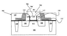
现在参考图4和图5,图中显示了金属栅极的形成的实施例。图4显示了器件400,器件400包括沉积到沟槽300中的金属栅极材料。金属栅极材料可以包括一个或多个材料层,例如衬层,向栅极提供合适工作函数的材料,栅电极材料和/或其他合适材料。但是,可以观察到,金属栅极形成所需的一个或多个层的沉积可以提供沟槽300的不彻底填充。例如,第一金属402,例如金属衬层和/或工作函数金属的沉积可以在沟槽300的开口上提供突起404。突起404可以导致填充高纵横比沟槽的困难。随后的金属层406的沉积可以在沟槽中形成一个或多个空隙,例如空隙408。Referring now to FIGS. 4 and 5 , embodiments of the formation of metal gates are shown. FIG. 4 shows
现在参考图5,在器件400上执行化学机械抛光(CMP)工艺,以提供器件500并形成金属栅极502。器件500显示了形成有空隙408的金属栅极502。虽然进一步的CMP处理可以减少空隙408,例如通过减少栅极高度,但是这可以导致其他问题,例如沟道上的应力减少(例如不利的减少用于应变器件的应力)和/或晶体管的性能可能被降低。Referring now to FIG. 5 , a chemical mechanical polishing (CMP) process is performed on
因此,图4和图5显示了后栅极工艺的缺点,其中所获得的沟槽的纵横比导致材料沉积以致局部或全部填充该沟槽是困难的。Thus, Figures 4 and 5 show a disadvantage of the gate-last process, where the aspect ratio of the trenches obtained makes deposition of material such that partial or complete filling of the trenches is difficult.
现在参考图6,该图显示了包括通过“后栅极”工艺形成金属栅极的方法600。方法600首先是步骤602,该步骤中形成有包括晶体管结构的器件。晶体管结构包括伪栅极结构。伪栅极结构可以包括伪多晶硅栅极结构。形成的器件可以基本上与上面参考图1描述的器件100类似。特别地,伪栅极结构可以基本上与上面参考图1描述的伪栅极结构118类似。Referring now to FIG. 6 , there is shown a
方法600然后前进到步骤604,在该步骤中执行CMP工艺。CMP工艺可以平整器件,并曝光伪栅极结构。产生的器件可以基本上与上面参考图2描述的器件200类似。
然后,方法600继续步骤606,在该步骤中伪栅极结构被除去。除去伪栅极可以形成内部形成可有金属栅极的沟槽(例如衬底中的开口)。产生的器件可以基本上与上面参考图3描述的器件300类似。特别地,沟槽可以与图3描述的沟槽302类似、沟槽的侧壁和底部可以涂覆有衬层。在一个实施例中,衬层可以是SiO2、SiN和/或其他合适材料。衬层可以包含在衬垫结构中。衬层可以基本上与上面参考图1描述的衬层117类似。
然后方法600前进至步骤608,在该步骤中,对步骤606中形成的沟槽的轮廓进行修正。沟槽的轮廓可以这样修正以使沟槽的开口(例如沟槽的顶部或开口)宽于沟槽的底部。沟槽轮廓可以使用溅射工艺、反应离子蚀刻和/或其他能够除去部分相邻层的合适工艺进行修正。溅射工艺可以利用物理气相沉积(PVD)工具执行。溅射工艺可以使用惰性离子,例如氩。在一个实施例中,使用包含等离子体的惰性气体修正轮廓。在一个实施例中,在室温下使用包括惰性气体(例如氩气)的溅射工艺。在一个实施例中,溅射工艺为多步骤工艺。例如,第一溅射工艺的射频功率可以为大约200到3000瓦特之间,然后减少该射频功率以用于包括在大约300到400瓦特之间的射频功率的第二溅射工艺。双阶段工艺可以在第一步骤中提供部分包围层(例如,电介质)的“粗”移除,并且第二步骤中可以精调沟槽的轮廓。
修正的轮廓包括沟槽的锥形侧壁。参考图7的例子,提供了修正轮廓的沟槽702。修正轮廓的沟槽702可以称为锥形轮廓沟槽。沟槽702包括开口处的宽度W1,该宽度大于沟槽底部的宽度W2。沟槽的侧壁,例如侧壁704从沟槽底部垂直延伸,然后以倾斜的方式延伸形成沟槽的顶部,如图示倾斜侧壁706。其他修正轮廓的实施例也是可行的,包括沟槽开口宽度大于沟槽底部宽度的例子。The modified profile includes tapered sidewalls of the trench. Referring to the example of FIG. 7 , a modified
方法600然后前进到步骤610,在该步骤中金属沉积到修正轮廓的沟槽中。沉积的金属可以是任意合适用于形成金属栅极或其部分,包括工作函数层、衬层、界面层、种子层、附着层、势垒层等的金属材料。金属栅极可以包括包含Ti、TiN、TaN、Ta、TaC、TaSiN、W、WN、MoN、MoON、RuO2和/或其他合适材料的一个或更多层。金属栅极可以包括通过PVD、CVD、ALD、平整化和/或其他合适工艺形成的一个或更多层。可以沉积的金属例如包括p型金属材料和n型金属材料。p型金属材料包括例如钌、钯、铂、钴、镍和导电金属氧化物的成分,和/或其他合适材料。n型金属材料包括例如铪、锆、钛、钽、铝、金属碳化物(例如碳化铪、碳化锆、碳化钛、碳化铝)、铝化物和/或其他合适材料。除n型和/或p型金属之外,可以沉积填充金属,从而基本上或者完全地填充沟槽的其余部分。填充金属可以包括氮化钛、钨、钛、铝、钽、氮化钽、钴、铜、镍和/或其他合适材料。填充金属可以使用CVD、PVD、平整化和/或其他合适工艺沉积。参考图8的例子,工作函数金属802和金属栅极填充材料804被沉积。沉积层基本上填充了上述步骤606和608提供的沟槽。注意到,第一沉积层(例如,工作函数金属802)提供了垂直侧壁(相比上面参考图4和图5描述的突起404)。
方法600然后前进到步骤612,该步骤中执行CMP工艺。CMP工艺对器件进行平整,平整化可以除去沉积在沟槽结构外侧的材料。参考图9的例子,平整化工艺提供了包括金属栅极结构902的器件900,该金属栅极结构902可以基本上没有空隙。金属栅极结构902包括工作函数金属802、金属栅极填充材料804和栅极电介质层110。金属栅极结构902具有修正轮廓。尤其,金属栅极结构902包括锥形,如图所示栅极顶部的宽度大于栅极底部。(请注意,顶部和底部为相对用语,并且目的不在于提供任何绝对方向限制。)
在实施例中,方法600可以继续包括例如封盖层的沉积、接触部的形成、互连结构(例如向包括形成金属栅极的器件提供电互连的线和通孔)等工艺步骤。In an embodiment, the
因此,方法600与图1-3和图7-9所示的器件可以改善金属栅极的形成,例如包括最小化和/或消除由图4和5分别显示的器件400和500提供的空隙的形成。空隙的减少可以通过修正内部形成有栅极的沟槽的轮廓来实现。该修正可以使得材料更容易在沟槽中沉积(例如通过CVD、平整化和/或其他合适方式)。形成的金属栅极包括修正的轮廓--锥形金属栅极。Accordingly,
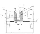
现在参考图10,该图显示了包括具有锥形轮廓的金属栅极1002的器件1000的实施例。器件1000可以使用方法600或者其部分步骤形成。器件1000包括衬底102、STI结构104、接触部112、衬垫116、栅极电介质110以及电介质层122,上述结构可以与图1描述的各个对应的特征基本上类似。器件1000还包括界面层1004、封盖层1006以及导电层1008。封盖层1006可以包括金属氧化物或者金属合金氧化物。在一个实施例中,封盖层1106可以调整栅极的工作函数。导电层1008可以包括金属氮化物、RuO2、Ti、Ta和/或其他合适材料。在其他实施例中,可以存在额外层,并且/或者可以省略一或多个上述层。界面层1004可以包括硅、氧和/或氮。Referring now to FIG. 10 , an embodiment of a
器件1000显示为锥形金属栅极结构,器件1000包括形成在锥形轮廓沟槽内部的金属栅极1002。具有锥形轮廓的金属栅极包括锥形侧壁,其中锥形侧壁提供栅极1002顶部大于栅极1002的底部(例如更靠近衬底)的宽度。侧壁包括用于栅电极距离h1的基本垂直的部分1002a,该基本垂直的部分1002a关于衬底102的表面具有大约90度的角度。在一个实施例中,垂直部1002a相对衬底102的表面具有大约85到90度之间的角度。侧壁还包括位于沟槽上部的基本倾斜的部分1002b,器件1000的侧壁1002b为弯曲状(圆形或弧形)。锥形轮廓提供了具有角度Ta的锥形(例如,减少垂直侧壁到与与弯曲的侧壁相切的假想线)。在一个实施例中,角度Ta大概为30度。在一个实施例中,角度Ta为大概20度到5度之间。虽然这里描述的是栅极的尺寸和结构,但是同样可以适用于描述锥形轮廓沟槽,例如上文参考图7描述的沟槽702,在其中形成了金属栅极。例如,角度Ta可以提供形成在衬底102、侧壁1002a和/或1002b上的沟槽的锥形角度,可以限定沟槽侧壁以及或者替代栅极。
现在参考图11,该图显示了包括金属栅极的器件1100的实施例。器件1100可以使用方法600或者其部分步骤形成。Referring now to FIG. 11 , an embodiment of a
器件1100包括具有锥形轮廓的金属栅极1102。锥形轮廓的金属栅极包括锥形侧壁,其中锥形侧壁提供栅极的顶部大于底部的宽度(例如最靠近衬底102的宽度减少)。栅极1102的侧壁包括用于距离h1的基本垂直的部分1102a,该基本垂直部1102a关于衬底102的表面具有大约90度的角度。在一个实施例中,垂直部1102a相对衬底102的表面具有大约85到90度之间的角度。侧壁还包括上部1102b,上部1102b为倾斜的,并延伸到栅极1102的顶部,器件1100的侧壁1002b的上部基本上为直线状(笔直的)。锥形轮廓提供了具有角度Tb(例如,角度位于垂直部1202a和锥形部1202b之间)的锥形。在一个实施例中,角度Tb大约为30度。在一个实施例中,角度Ta为大约30度到5度之间。在一个实施例中,角度Tb为大约5度到20度之间。虽然这里描述的是栅极的尺寸和结构,但是同样可以适用于描述锥形轮廓沟槽,例如上文参考图7描述的沟槽702,其中形成了金属栅极。例如,角度Tb可以提供形成在衬底102、侧壁1102a和/或1102b上的沟槽锥形角度,可以限定沟槽侧壁以及或者替代栅极。
总之,可以执行后栅极工艺用来形成金属栅极结构。通过修正金属栅极结构形成于其中的沟槽开口(例如上开口),可以减少形成金属栅极结构所产生的问题。尤其,可以修正沟槽轮廓从而使得材料更容易地沉积到沟槽中。可以修改沟槽轮廓,从而向与剩余沟槽宽度,包括沟槽底部宽度相比具有增加的沟槽宽度的沟槽提供开口。有此,形成的栅极结构包括锥形轮廓。In conclusion, a gate last process may be performed to form the metal gate structure. Problems associated with forming metal gate structures can be reduced by modifying the trench openings (eg, upper openings) in which the metal gate structures are formed. In particular, trench profiles can be modified to allow easier deposition of material into the trenches. The groove profile may be modified to provide an opening to the groove with an increased groove width compared to the remaining groove width, including the groove bottom width. With this, the formed gate structure includes a tapered profile.
因此,本发明提供了包括修正的沟槽结构的器件和方法,该修正的沟槽结构防止或减少在后栅极工艺中不完全形成金属栅极的风险。虽然上文描述显示和描述了一个或多个实施例,但是对于本领域的普通技术人员而言,可以理解在不脱离本发明的原理和精神的情况下可以对这些实施例进行多种形式和细节的变化。因此,本发明的权利要求应当与本发明公开一致以更广泛的形式进行解释。Accordingly, the present invention provides devices and methods that include a modified trench structure that prevents or reduces the risk of incomplete formation of a metal gate in a gate-last process. While the foregoing description shows and describes one or more embodiments, it would be appreciated by those of ordinary skill in the art that these embodiments can be modified in various forms and without departing from the principles and spirit of the invention. Variations in details. Therefore, the claims of the present invention should be interpreted in a broader form consistent with the present disclosure.
Claims (13)
Translated fromChineseApplications Claiming Priority (4)
| Application Number | Priority Date | Filing Date | Title |
|---|---|---|---|
| US9046908P | 2008-08-20 | 2008-08-20 | |
| US61/090,469 | 2008-08-20 | ||
| US12/276,015US8735235B2 (en) | 2008-08-20 | 2008-11-21 | Integrated circuit metal gate structure and method of fabrication |
| US12/276,015 | 2008-11-21 |
Publications (2)
| Publication Number | Publication Date |
|---|---|
| CN101656205A CN101656205A (en) | 2010-02-24 |
| CN101656205Btrue CN101656205B (en) | 2013-07-24 |
Family
ID=41695552
Family Applications (1)
| Application Number | Title | Priority Date | Filing Date |
|---|---|---|---|
| CN2009101617633AActiveCN101656205B (en) | 2008-08-20 | 2009-08-14 | Integrated circuit metal gate structure and method of fabrication |
Country Status (2)
| Country | Link |
|---|---|
| US (2) | US8735235B2 (en) |
| CN (1) | CN101656205B (en) |
Families Citing this family (94)
| Publication number | Priority date | Publication date | Assignee | Title |
|---|---|---|---|---|
| US7964487B2 (en)* | 2008-06-04 | 2011-06-21 | International Business Machines Corporation | Carrier mobility enhanced channel devices and method of manufacture |
| DE102009043628B4 (en)* | 2009-09-30 | 2011-12-01 | Globalfoundries Dresden Module One Llc & Co. Kg | Improved filling conditions in an exchange gate method by carrying out a sacrificial filler based polishing process |
| US8357603B2 (en)* | 2009-12-18 | 2013-01-22 | Taiwan Semiconductor Manufacturing Company, Ltd. | Metal gate fill and method of making |
| CN102194693B (en)* | 2010-03-16 | 2013-05-22 | 中国科学院微电子研究所 | A kind of semiconductor device and its manufacturing method |
| KR20120019917A (en)* | 2010-08-27 | 2012-03-07 | 삼성전자주식회사 | Method of fabricating semiconductor device |
| CN102386081B (en)* | 2010-09-02 | 2013-07-17 | 中芯国际集成电路制造(上海)有限公司 | Method for forming metal gate |
| KR101675392B1 (en) | 2010-10-12 | 2016-11-14 | 삼성전자 주식회사 | Method for manufacturing semiconductor device |
| US9105653B2 (en)* | 2010-10-18 | 2015-08-11 | Taiwan Semiconductor Manufacturing Company, Ltd. | Method for fabricating a metal gate electrode |
| CN102479693B (en) | 2010-11-30 | 2013-11-06 | 中芯国际集成电路制造(北京)有限公司 | Gate forming method |
| CN102479692B (en)* | 2010-11-30 | 2014-06-04 | 中芯国际集成电路制造(北京)有限公司 | Gate forming method |
| CN102486998B (en)* | 2010-12-01 | 2014-07-02 | 中芯国际集成电路制造(上海)有限公司 | Method for forming grid |
| CN102487013B (en)* | 2010-12-02 | 2014-07-02 | 中芯国际集成电路制造(北京)有限公司 | Method for forming grid |
| US8574990B2 (en) | 2011-02-24 | 2013-11-05 | United Microelectronics Corp. | Method of manufacturing semiconductor device having metal gate |
| US8802524B2 (en) | 2011-03-22 | 2014-08-12 | United Microelectronics Corp. | Method of manufacturing semiconductor device having metal gates |
| US8466502B2 (en) | 2011-03-24 | 2013-06-18 | United Microelectronics Corp. | Metal-gate CMOS device |
| US8710596B2 (en) | 2011-05-13 | 2014-04-29 | United Microelectronics Corp. | Semiconductor device |
| US8597860B2 (en) | 2011-05-20 | 2013-12-03 | United Microelectronics Corp. | Dummy patterns and method for generating dummy patterns |
| US20120319198A1 (en) | 2011-06-16 | 2012-12-20 | Chin-Cheng Chien | Semiconductor device and fabrication method thereof |
| US8674452B2 (en) | 2011-06-24 | 2014-03-18 | United Microelectronics Corp. | Semiconductor device with lower metal layer thickness in PMOS region |
| US8486790B2 (en) | 2011-07-18 | 2013-07-16 | United Microelectronics Corp. | Manufacturing method for metal gate |
| US8580625B2 (en) | 2011-07-22 | 2013-11-12 | Tsuo-Wen Lu | Metal oxide semiconductor transistor and method of manufacturing the same |
| CN102931064B (en)* | 2011-08-12 | 2015-04-29 | 中芯国际集成电路制造(上海)有限公司 | Metal gate forming method |
| US8853013B2 (en) | 2011-08-19 | 2014-10-07 | United Microelectronics Corp. | Method for fabricating field effect transistor with fin structure |
| US8477006B2 (en) | 2011-08-30 | 2013-07-02 | United Microelectronics Corp. | Resistor and manufacturing method thereof |
| CN102983097B (en)* | 2011-09-05 | 2015-02-18 | 中芯国际集成电路制造(上海)有限公司 | Method for producing metal plug for metal gate |
| CN103000504A (en)* | 2011-09-14 | 2013-03-27 | 中国科学院微电子研究所 | Semiconductor device and method for manufacturing the same |
| US8507350B2 (en) | 2011-09-21 | 2013-08-13 | United Microelectronics Corporation | Fabricating method of semiconductor elements |
| US8497198B2 (en) | 2011-09-23 | 2013-07-30 | United Microelectronics Corp. | Semiconductor process |
| US8722501B2 (en) | 2011-10-18 | 2014-05-13 | United Microelectronics Corp. | Method for manufacturing multi-gate transistor device |
| US8871575B2 (en) | 2011-10-31 | 2014-10-28 | United Microelectronics Corp. | Method of fabricating field effect transistor with fin structure |
| US9006092B2 (en) | 2011-11-03 | 2015-04-14 | United Microelectronics Corp. | Semiconductor structure having fluoride metal layer and process thereof |
| US8975672B2 (en)* | 2011-11-09 | 2015-03-10 | United Microelectronics Corp. | Metal oxide semiconductor transistor and manufacturing method thereof |
| CN103117213B (en)* | 2011-11-16 | 2015-10-07 | 中芯国际集成电路制造(上海)有限公司 | Method for forming metallic grid |
| US8658487B2 (en) | 2011-11-17 | 2014-02-25 | United Microelectronics Corp. | Semiconductor device and fabrication method thereof |
| US8921206B2 (en) | 2011-11-30 | 2014-12-30 | United Microelectronics Corp. | Semiconductor process |
| US9698229B2 (en) | 2012-01-17 | 2017-07-04 | United Microelectronics Corp. | Semiconductor structure and process thereof |
| US8536072B2 (en) | 2012-02-07 | 2013-09-17 | United Microelectronics Corp. | Semiconductor process |
| US8987096B2 (en) | 2012-02-07 | 2015-03-24 | United Microelectronics Corp. | Semiconductor process |
| US8860135B2 (en) | 2012-02-21 | 2014-10-14 | United Microelectronics Corp. | Semiconductor structure having aluminum layer with high reflectivity |
| US8860181B2 (en) | 2012-03-07 | 2014-10-14 | United Microelectronics Corp. | Thin film resistor structure |
| US9006107B2 (en) | 2012-03-11 | 2015-04-14 | United Microelectronics Corp. | Patterned structure of semiconductor device and fabricating method thereof |
| US9142649B2 (en) | 2012-04-23 | 2015-09-22 | United Microelectronics Corp. | Semiconductor structure with metal gate and method of fabricating the same |
| KR101909091B1 (en)* | 2012-05-11 | 2018-10-17 | 삼성전자 주식회사 | Semiconductor device and fabricating method thereof |
| US8836049B2 (en) | 2012-06-13 | 2014-09-16 | United Microelectronics Corp. | Semiconductor structure and process thereof |
| US8501636B1 (en) | 2012-07-24 | 2013-08-06 | United Microelectronics Corp. | Method for fabricating silicon dioxide layer |
| US9064931B2 (en) | 2012-10-11 | 2015-06-23 | United Microelectronics Corp. | Semiconductor structure having contact plug and metal gate transistor and method of making the same |
| US8927388B2 (en) | 2012-11-15 | 2015-01-06 | United Microelectronics Corp. | Method of fabricating dielectric layer and shallow trench isolation |
| US8890262B2 (en)* | 2012-11-29 | 2014-11-18 | Globalfoundries Inc. | Semiconductor device having a metal gate recess |
| US9054172B2 (en) | 2012-12-05 | 2015-06-09 | United Microelectrnics Corp. | Semiconductor structure having contact plug and method of making the same |
| US8883621B2 (en) | 2012-12-27 | 2014-11-11 | United Microelectronics Corp. | Semiconductor structure and method of fabricating MOS device |
| US8735269B1 (en) | 2013-01-15 | 2014-05-27 | United Microelectronics Corp. | Method for forming semiconductor structure having TiN layer |
| US9202691B2 (en) | 2013-01-18 | 2015-12-01 | Taiwan Semiconductor Manufacturing Company, Ltd. | Semiconductor device having modified profile metal gate |
| US9076870B2 (en) | 2013-02-21 | 2015-07-07 | United Microelectronics Corp. | Method for forming fin-shaped structure |
| US9196352B2 (en) | 2013-02-25 | 2015-11-24 | United Microelectronics Corp. | Static random access memory unit cell structure and static random access memory unit cell layout structure |
| US20140246734A1 (en)* | 2013-03-01 | 2014-09-04 | Globalfoundries Inc. | Replacement metal gate with mulitiple titanium nitride laters |
| US9214395B2 (en) | 2013-03-13 | 2015-12-15 | United Microelectronics Corp. | Method of manufacturing semiconductor devices |
| US8753902B1 (en) | 2013-03-13 | 2014-06-17 | United Microelectronics Corp. | Method of controlling etching process for forming epitaxial structure |
| US9093285B2 (en) | 2013-03-22 | 2015-07-28 | United Microelectronics Corp. | Semiconductor structure and process thereof |
| KR20140121634A (en)* | 2013-04-08 | 2014-10-16 | 삼성전자주식회사 | Semiconductor device and fabricating method thereof |
| US9023708B2 (en) | 2013-04-19 | 2015-05-05 | United Microelectronics Corp. | Method of forming semiconductor device |
| US9147747B2 (en) | 2013-05-02 | 2015-09-29 | United Microelectronics Corp. | Semiconductor structure with hard mask disposed on the gate structure |
| US9159798B2 (en) | 2013-05-03 | 2015-10-13 | United Microelectronics Corp. | Replacement gate process and device manufactured using the same |
| US9230812B2 (en) | 2013-05-22 | 2016-01-05 | United Microelectronics Corp. | Method for forming semiconductor structure having opening |
| US9196542B2 (en) | 2013-05-22 | 2015-11-24 | United Microelectronics Corp. | Method for manufacturing semiconductor devices |
| US8993433B2 (en) | 2013-05-27 | 2015-03-31 | United Microelectronics Corp. | Manufacturing method for forming a self aligned contact |
| US9349812B2 (en) | 2013-05-27 | 2016-05-24 | United Microelectronics Corp. | Semiconductor device with self-aligned contact and method of manufacturing the same |
| US8921947B1 (en) | 2013-06-10 | 2014-12-30 | United Microelectronics Corp. | Multi-metal gate semiconductor device having triple diameter metal opening |
| US9064814B2 (en) | 2013-06-19 | 2015-06-23 | United Microelectronics Corp. | Semiconductor structure having metal gate and manufacturing method thereof |
| US9257348B2 (en)* | 2013-08-06 | 2016-02-09 | Globalfoundries Inc. | Methods of forming replacement gate structures for transistors and the resulting devices |
| US9245972B2 (en) | 2013-09-03 | 2016-01-26 | United Microelectronics Corp. | Method for manufacturing semiconductor device |
| US9384984B2 (en) | 2013-09-03 | 2016-07-05 | United Microelectronics Corp. | Semiconductor structure and method of forming the same |
| US20150069534A1 (en) | 2013-09-11 | 2015-03-12 | United Microelectronics Corp. | Semiconductor device and method for fabricating the same |
| US9281201B2 (en) | 2013-09-18 | 2016-03-08 | United Microelectronics Corp. | Method of manufacturing semiconductor device having metal gate |
| KR102167625B1 (en)* | 2013-10-24 | 2020-10-19 | 삼성전자주식회사 | Semiconductor devices and methods of manufacturing the same |
| US20150118836A1 (en)* | 2013-10-28 | 2015-04-30 | United Microelectronics Corp. | Method of fabricating semiconductor device |
| US9425048B2 (en) | 2013-11-06 | 2016-08-23 | Taiwan Semiconductor Manufacturing Co., Ltd. | Mechanisms for semiconductor device structure |
| US9318490B2 (en) | 2014-01-13 | 2016-04-19 | United Microelectronics Corp. | Semiconductor structure and manufacturing method thereof |
| US9231071B2 (en) | 2014-02-24 | 2016-01-05 | United Microelectronics Corp. | Semiconductor structure and manufacturing method of the same |
| TWI625792B (en)* | 2014-06-09 | 2018-06-01 | 聯華電子股份有限公司 | Semiconductor component and manufacturing method thereof |
| DE102014117242A1 (en)* | 2014-11-25 | 2016-05-25 | Infineon Technologies Dresden Gmbh | Power transistor with field electrode |
| CN105826176B (en)* | 2015-01-06 | 2018-10-16 | 中芯国际集成电路制造(上海)有限公司 | Semiconductor structure and forming method thereof |
| US9449921B1 (en) | 2015-12-15 | 2016-09-20 | International Business Machines Corporation | Voidless contact metal structures |
| US10083961B2 (en)* | 2016-09-07 | 2018-09-25 | International Business Machines Corporation | Gate cut with integrated etch stop layer |
| US9929250B1 (en) | 2016-09-27 | 2018-03-27 | International Business Machines Corporation | Semiconductor device including optimized gate stack profile |
| CN109148374B (en)* | 2017-06-28 | 2021-04-23 | 中芯国际集成电路制造(上海)有限公司 | A method of manufacturing a semiconductor device |
| US10418453B2 (en)* | 2017-11-22 | 2019-09-17 | Taiwan Semiconductor Manufacturing Co., Ltd. | Forming metal contacts on metal gates |
| US10332747B1 (en) | 2018-01-24 | 2019-06-25 | Globalfoundries Inc. | Selective titanium nitride deposition using oxides of lanthanum masks |
| US11152384B2 (en)* | 2019-01-15 | 2021-10-19 | Taiwan Semiconductor Manufacturing Company, Ltd. | Boundary structure for embedded memory |
| US11075299B2 (en) | 2019-07-01 | 2021-07-27 | International Business Machines Corporation | Transistor gate having tapered segments positioned above the fin channel |
| US11018256B2 (en)* | 2019-08-23 | 2021-05-25 | Taiwan Semiconductor Manufacturing Co., Ltd. | Selective internal gate structure for ferroelectric semiconductor devices |
| DE102020114867B4 (en) | 2020-01-29 | 2025-03-13 | Taiwan Semiconductor Manufacturing Co., Ltd. | PROCEDURE |
| US11398384B2 (en)* | 2020-02-11 | 2022-07-26 | Taiwan Semiconductor Manufacturing Company, Ltd. | Methods for manufacturing a transistor gate by non-directional implantation of impurities in a gate spacer |
| DE102020122120A1 (en)* | 2020-02-18 | 2021-08-19 | Taiwan Semiconductor Manufacturing Co., Ltd. | METAL GATE STRUCTURES AND METHODS OF MANUFACTURING THE SAME IN FIELD EFFECT TRANSISTORS |
| US11476351B2 (en)* | 2020-02-18 | 2022-10-18 | Taiwan Semiconductor Manufacturing Co., Ltd. | Metal gate structures and methods of fabricating the same in field-effect transistors |
Citations (7)
| Publication number | Priority date | Publication date | Assignee | Title |
|---|---|---|---|---|
| US5960270A (en)* | 1997-08-11 | 1999-09-28 | Motorola, Inc. | Method for forming an MOS transistor having a metallic gate electrode that is formed after the formation of self-aligned source and drain regions |
| CN1319881A (en)* | 2000-03-09 | 2001-10-31 | 三星电子株式会社 | Method for forming self-aligning contact welding disc in metal inlay grid technology |
| US6642590B1 (en)* | 2000-10-19 | 2003-11-04 | Advanced Micro Devices, Inc. | Metal gate with PVD amorphous silicon layer and barrier layer for CMOS devices and method of making with a replacement gate process |
| CN1476064A (en)* | 2002-08-14 | 2004-02-18 | 上海宏力半导体制造有限公司 | Method of forming light doped drain electrode using inverse taper grid structure |
| CN1846313A (en)* | 2003-09-09 | 2006-10-11 | 国际商业机器公司 | Structures and methods for metal replacement gates for high performance devices |
| CN101006579A (en)* | 2004-08-25 | 2007-07-25 | 英特尔公司 | Forming integrated circuits with replacement metal gate electrodes |
| CN100373591C (en)* | 2005-02-09 | 2008-03-05 | 台湾积体电路制造股份有限公司 | Method for manufacturing capacitor and metal gate of semiconductor device |
Family Cites Families (14)
| Publication number | Priority date | Publication date | Assignee | Title |
|---|---|---|---|---|
| US5393682A (en) | 1993-12-13 | 1995-02-28 | Taiwan Semiconductor Manufacturing Company | Method of making tapered poly profile for TFT device manufacturing |
| FR2757312B1 (en)* | 1996-12-16 | 1999-01-08 | Commissariat Energie Atomique | SELF-ALIGNED METAL GRID TRANSISTOR AND MANUFACTURING METHOD THEREOF |
| US6200860B1 (en) | 1999-05-03 | 2001-03-13 | Taiwan Semiconductor Manufacturing Company | Process for preventing the reverse tunneling during programming in split gate flash |
| TW449920B (en)* | 2000-07-07 | 2001-08-11 | Amic Technology Taiwan Inc | Method for manufacturing MOS transistor |
| US7303996B2 (en)* | 2003-10-01 | 2007-12-04 | Taiwan Semiconductor Manufacturing Co., Ltd. | High-K gate dielectric stack plasma treatment to adjust threshold voltage characteristics |
| US6974736B2 (en)* | 2004-01-09 | 2005-12-13 | International Business Machines Corporation | Method of forming FET silicide gate structures incorporating inner spacers |
| KR100574338B1 (en)* | 2004-01-19 | 2006-04-26 | 삼성전자주식회사 | Metal gate formation method of semiconductor device |
| US7208361B2 (en)* | 2004-03-24 | 2007-04-24 | Intel Corporation | Replacement gate process for making a semiconductor device that includes a metal gate electrode |
| US7176090B2 (en)* | 2004-09-07 | 2007-02-13 | Intel Corporation | Method for making a semiconductor device that includes a metal gate electrode |
| US7332407B2 (en)* | 2004-12-23 | 2008-02-19 | Taiwan Semiconductor Manufacturing Company, Ltd. | Method and apparatus for a semiconductor device with a high-k gate dielectric |
| US7517746B2 (en)* | 2007-04-24 | 2009-04-14 | United Microelectronics Corp. | Metal oxide semiconductor transistor with Y shape metal gate and fabricating method thereof |
| US8901665B2 (en) | 2011-12-22 | 2014-12-02 | Taiwan Semiconductor Manufacturing Company, Ltd. | Gate structure for semiconductor device |
| US9136349B2 (en) | 2012-01-06 | 2015-09-15 | Taiwan Semiconductor Manufacturing Company, Ltd. | Dummy gate structure for semiconductor devices |
| US8629512B2 (en) | 2012-03-28 | 2014-01-14 | Taiwan Semiconductor Manufacturing Company, Ltd. | Gate stack of fin field effect transistor with slanted sidewalls |
- 2008
- 2008-11-21USUS12/276,015patent/US8735235B2/enactiveActive
- 2009
- 2009-08-14CNCN2009101617633Apatent/CN101656205B/enactiveActive
- 2014
- 2014-05-22USUS14/284,559patent/US9455344B2/enactiveActive
Patent Citations (7)
| Publication number | Priority date | Publication date | Assignee | Title |
|---|---|---|---|---|
| US5960270A (en)* | 1997-08-11 | 1999-09-28 | Motorola, Inc. | Method for forming an MOS transistor having a metallic gate electrode that is formed after the formation of self-aligned source and drain regions |
| CN1319881A (en)* | 2000-03-09 | 2001-10-31 | 三星电子株式会社 | Method for forming self-aligning contact welding disc in metal inlay grid technology |
| US6642590B1 (en)* | 2000-10-19 | 2003-11-04 | Advanced Micro Devices, Inc. | Metal gate with PVD amorphous silicon layer and barrier layer for CMOS devices and method of making with a replacement gate process |
| CN1476064A (en)* | 2002-08-14 | 2004-02-18 | 上海宏力半导体制造有限公司 | Method of forming light doped drain electrode using inverse taper grid structure |
| CN1846313A (en)* | 2003-09-09 | 2006-10-11 | 国际商业机器公司 | Structures and methods for metal replacement gates for high performance devices |
| CN101006579A (en)* | 2004-08-25 | 2007-07-25 | 英特尔公司 | Forming integrated circuits with replacement metal gate electrodes |
| CN100373591C (en)* | 2005-02-09 | 2008-03-05 | 台湾积体电路制造股份有限公司 | Method for manufacturing capacitor and metal gate of semiconductor device |
Also Published As
| Publication number | Publication date |
|---|---|
| US9455344B2 (en) | 2016-09-27 |
| US20100044783A1 (en) | 2010-02-25 |
| CN101656205A (en) | 2010-02-24 |
| US20140246712A1 (en) | 2014-09-04 |
| US8735235B2 (en) | 2014-05-27 |
Similar Documents
| Publication | Publication Date | Title |
|---|---|---|
| CN101656205B (en) | Integrated circuit metal gate structure and method of fabrication | |
| CN101789368B (en) | Semiconductor element and its manufacturing method | |
| US7939392B2 (en) | Method for gate height control in a gate last process | |
| CN103854990B (en) | Methods for fabricating integrated circuits having low resistance metal gate structures | |
| US7923321B2 (en) | Method for gap filling in a gate last process | |
| US9391075B2 (en) | Integrated circuit and method for fabricating the same having a replacement gate structure | |
| JP5503517B2 (en) | Method for manufacturing field effect transistor | |
| US8093116B2 (en) | Method for N/P patterning in a gate last process | |
| US10923393B2 (en) | Contacts and interconnect structures in field-effect transistors | |
| US9425285B2 (en) | Fabricating method of semiconductor device | |
| CN101661936B (en) | Semiconductor device and manufacturing method thereof | |
| US8455952B2 (en) | Spacer elements for semiconductor device | |
| US8008145B2 (en) | High-K metal gate structure fabrication method including hard mask | |
| CN102903742B (en) | The metal gate electrode of field-effect transistor | |
| US20140110798A1 (en) | Methods of forming a semiconductor device with low-k spacers and the resulting device | |
| US20120018848A1 (en) | High surface dopant concentration semiconductor device and method of fabricating | |
| CN100580892C (en) | MOS transistor with Y-type metal gate and its process | |
| CN118380380A (en) | Semiconductor device and method of forming the same | |
| CN101673677B (en) | semiconductor manufacturing method | |
| CN113270364A (en) | Method for manufacturing semiconductor device |
Legal Events
| Date | Code | Title | Description |
|---|---|---|---|
| C06 | Publication | ||
| PB01 | Publication | ||
| C10 | Entry into substantive examination | ||
| SE01 | Entry into force of request for substantive examination | ||
| C14 | Grant of patent or utility model | ||
| GR01 | Patent grant |