CN101655720B - Personal digital assistant - Google Patents
Personal digital assistantDownload PDFInfo
- Publication number
- CN101655720B CN101655720BCN2008101420230ACN200810142023ACN101655720BCN 101655720 BCN101655720 BCN 101655720BCN 2008101420230 ACN2008101420230 ACN 2008101420230ACN 200810142023 ACN200810142023 ACN 200810142023ACN 101655720 BCN101655720 BCN 101655720B
- Authority
- CN
- China
- Prior art keywords
- screen
- layer
- carbon nanotube
- touch
- personal digital
- Prior art date
- Legal status (The legal status is an assumption and is not a legal conclusion. Google has not performed a legal analysis and makes no representation as to the accuracy of the status listed.)
- Expired - Fee Related
Links
Images


Classifications
- G—PHYSICS
- G06—COMPUTING OR CALCULATING; COUNTING
- G06F—ELECTRIC DIGITAL DATA PROCESSING
- G06F3/00—Input arrangements for transferring data to be processed into a form capable of being handled by the computer; Output arrangements for transferring data from processing unit to output unit, e.g. interface arrangements
- G06F3/01—Input arrangements or combined input and output arrangements for interaction between user and computer
- G06F3/03—Arrangements for converting the position or the displacement of a member into a coded form
- G06F3/041—Digitisers, e.g. for touch screens or touch pads, characterised by the transducing means
- G06F3/045—Digitisers, e.g. for touch screens or touch pads, characterised by the transducing means using resistive elements, e.g. a single continuous surface or two parallel surfaces put in contact
- G—PHYSICS
- G06—COMPUTING OR CALCULATING; COUNTING
- G06F—ELECTRIC DIGITAL DATA PROCESSING
- G06F1/00—Details not covered by groups G06F3/00 - G06F13/00 and G06F21/00
- G06F1/16—Constructional details or arrangements
- G06F1/1613—Constructional details or arrangements for portable computers
- G06F1/1626—Constructional details or arrangements for portable computers with a single-body enclosure integrating a flat display, e.g. Personal Digital Assistants [PDAs]
- G—PHYSICS
- G06—COMPUTING OR CALCULATING; COUNTING
- G06F—ELECTRIC DIGITAL DATA PROCESSING
- G06F1/00—Details not covered by groups G06F3/00 - G06F13/00 and G06F21/00
- G06F1/16—Constructional details or arrangements
- G06F1/1613—Constructional details or arrangements for portable computers
- G06F1/1633—Constructional details or arrangements of portable computers not specific to the type of enclosures covered by groups G06F1/1615 - G06F1/1626
- G06F1/1637—Details related to the display arrangement, including those related to the mounting of the display in the housing
- G06F1/1643—Details related to the display arrangement, including those related to the mounting of the display in the housing the display being associated to a digitizer, e.g. laptops that can be used as penpads
- G—PHYSICS
- G06—COMPUTING OR CALCULATING; COUNTING
- G06F—ELECTRIC DIGITAL DATA PROCESSING
- G06F2203/00—Indexing scheme relating to G06F3/00 - G06F3/048
- G06F2203/041—Indexing scheme relating to G06F3/041 - G06F3/045
- G06F2203/04107—Shielding in digitiser, i.e. guard or shielding arrangements, mostly for capacitive touchscreens, e.g. driven shields, driven grounds
- G—PHYSICS
- G06—COMPUTING OR CALCULATING; COUNTING
- G06F—ELECTRIC DIGITAL DATA PROCESSING
- G06F3/00—Input arrangements for transferring data to be processed into a form capable of being handled by the computer; Output arrangements for transferring data from processing unit to output unit, e.g. interface arrangements
- G06F3/01—Input arrangements or combined input and output arrangements for interaction between user and computer
- G06F3/03—Arrangements for converting the position or the displacement of a member into a coded form
- G06F3/041—Digitisers, e.g. for touch screens or touch pads, characterised by the transducing means
- G06F3/0416—Control or interface arrangements specially adapted for digitisers
Landscapes
- Engineering & Computer Science (AREA)
- Theoretical Computer Science (AREA)
- General Engineering & Computer Science (AREA)
- Computer Hardware Design (AREA)
- Human Computer Interaction (AREA)
- Physics & Mathematics (AREA)
- General Physics & Mathematics (AREA)
- Position Input By Displaying (AREA)
- Carbon And Carbon Compounds (AREA)
Abstract
Translated fromChinese
Description
Translated fromChinese技术领域technical field
本发明涉及一种个人数字助理,尤其涉及一种基于碳纳米管的触摸式个人数字助理。The invention relates to a personal digital assistant, in particular to a touch-type personal digital assistant based on carbon nanotubes.
背景技术Background technique
通常,个人数字助理(Personal Digital Assistant,PDA)作为便携式电子设备,组合了收集、存储、处理和交换信息的功能。现有的PDA一般为触摸式PDA,且根据其具体的应用会有不同的组成。一般地,所述PDA包括一本体、一设置于本体表面的显示屏及一设置于本体表面的输入设备,如一触摸屏。Generally, a Personal Digital Assistant (PDA) is a portable electronic device that combines the functions of collecting, storing, processing and exchanging information. Existing PDAs are generally touch-type PDAs, and have different compositions according to their specific applications. Generally, the PDA includes a body, a display screen arranged on the surface of the body, and an input device, such as a touch screen, arranged on the surface of the body.
作为PDA的主要输入设备,现有技术中的触摸屏按其工作原理和传输介质的不同,通常分为四种类型,分别为电阻式、电容感应式、红外线式以及表面声波式。其中电阻式触摸屏及电容式触摸屏由于其具有高分辨率、高灵敏度及耐用性等优点,被广泛应用在PDA中。As the main input device of PDA, touch screens in the prior art are generally divided into four types according to their working principles and transmission media, namely resistive type, capacitive sensing type, infrared type and surface acoustic wave type. Among them, resistive touch screens and capacitive touch screens are widely used in PDAs due to their advantages of high resolution, high sensitivity and durability.
然而,现有技术中的电容式和电阻式触摸屏通常包括一个作为透明导电层的铟锡氧化物层(ITO层),其采用离子束溅射或蒸镀等工艺制备,KazuhiroNoda等在文献Production of Transparent Conductive Films with Inserted SiO2Anchor Layer,and Application to a Resistive Touch Panel(Electronics andCommunications in Japan,Part 2,Vol.84,P39-45(2001))中介绍了一种采用ITO/SiO2/PET层的触摸屏。该ITO层在制备的过程,需要较高的真空环境及需要加热到200~300℃,因此,使得ITO层的制备成本较高。此外,现有技术中的ITO层作为透明导电层具有机械性能不够好、难以弯曲及阻值分布不均匀等缺点。另外,ITO在潮湿的空气中透明度会逐渐下降。从而导致现有的触摸屏及使用该触摸屏的PDA存在耐用性不够好,灵敏度低、线性及准确性较差等缺点。However, capacitive and resistive touch screens in the prior art usually include an indium tin oxide layer (ITO layer) as a transparent conductive layer, which is prepared by ion beam sputtering or evaporation, KazuhiroNoda et al. in the literature Production of Transparent Conductive Films with Inserted SiO2 Anchor Layer, and Application to a Resistive Touch Panel (Electronics and Communications in Japan, Part 2, Vol.84, P39-45 (2001)) introduces an ITO/SiO2 /PET layer touch screen. During the preparation process of the ITO layer, a relatively high vacuum environment and heating to 200-300° C. are required, therefore, the preparation cost of the ITO layer is relatively high. In addition, as a transparent conductive layer, the ITO layer in the prior art has disadvantages such as insufficient mechanical properties, difficulty in bending, uneven resistance distribution, and the like. In addition, the transparency of ITO will gradually decrease in humid air. As a result, existing touch screens and PDAs using the same have disadvantages such as insufficient durability, low sensitivity, poor linearity and accuracy.
因此,确有必要提供一种PDA,该PDA所采用的触摸屏具有耐用性好、灵敏度高、线性及准确性强的优点。Therefore, it is necessary to provide a PDA whose touch screen has the advantages of good durability, high sensitivity, strong linearity and high accuracy.
发明内容Contents of the invention
一种个人数字助理,包括:一本体,该本体上设置有一显示屏;以及一触摸屏,该触摸屏设置于所述显示屏表面,该触摸屏包括至少一透明导电层;其中,所述触摸屏中的透明导电层为一碳纳米管层。A personal digital assistant, comprising: a body, a display screen is arranged on the body; and a touch screen, the touch screen is arranged on the surface of the display screen, and the touch screen includes at least one transparent conductive layer; wherein, the transparent The conductive layer is a carbon nanotube layer.
本技术方案实施例提供的采用碳纳米管层作为透明导电层的个人数字助理具有以下优点:其一,由于碳纳米管层在潮湿的条件下具有良好的透明度,故采用碳纳米管层作为触摸屏的透明导电层,可以使应用该触摸屏的个人数字助理具有较好的透明度;其二,由于碳纳米管具有优异的力学性能,则由碳纳米管组成的碳纳米管层具有较好的韧性及机械强度,故采用该碳纳米管层作为触摸屏的透明导电层,可以相应的提高触摸屏的耐用性,进而提高使用该触摸屏的个人数字助理的耐用性;其三,由于碳纳米管具有优异的导电性能,则由碳纳米管组成的碳纳米管层具有均匀的阻值分布,因而,采用上述碳纳米管层作透明导电层,可以相应的提高触摸屏的分辨率和精确度,进而提高应用该触摸屏的个人数字助理的分辨率和精确度。The personal digital assistant using the carbon nanotube layer as the transparent conductive layer provided by the embodiment of the technical solution has the following advantages: First, because the carbon nanotube layer has good transparency under humid conditions, the carbon nanotube layer is used as the touch screen The transparent conductive layer can make the personal digital assistant using the touch screen have better transparency; second, because carbon nanotubes have excellent mechanical properties, the carbon nanotube layer composed of carbon nanotubes has better toughness and Mechanical strength, so using the carbon nanotube layer as the transparent conductive layer of the touch screen can correspondingly improve the durability of the touch screen, and then improve the durability of the personal digital assistant using the touch screen; third, because the carbon nanotube has excellent conductivity Performance, the carbon nanotube layer composed of carbon nanotubes has a uniform resistance distribution, therefore, using the above-mentioned carbon nanotube layer as a transparent conductive layer can correspondingly improve the resolution and accuracy of the touch screen, and then improve the application of the touch screen. The resolution and precision of a personal digital assistant.
附图说明Description of drawings
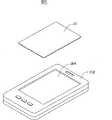
图1是本技术方案实施例个人数字助理的结构示意图。Fig. 1 is a schematic structural diagram of a personal digital assistant according to an embodiment of the technical solution.
图2是本技术方案实施例个人数字助理的控制方框图。Fig. 2 is a control block diagram of the personal digital assistant of the embodiment of the technical solution.
图3是本技术方案第一实施例个人数字助理中的触摸屏的立体结构示意图。Fig. 3 is a perspective structural diagram of a touch screen in a personal digital assistant according to the first embodiment of the technical solution.
图4是本技术方案第一实施例个人数字助理中的触摸屏的侧视结构示意图。Fig. 4 is a schematic side view structural diagram of the touch screen in the personal digital assistant according to the first embodiment of the technical solution.
图5是本技术方案第一实施例个人数字助理中碳纳米管薄膜的扫描电镜照片。Fig. 5 is a scanning electron micrograph of a carbon nanotube film in a personal digital assistant according to the first embodiment of the technical solution.
图6是本技术方案第一实施例个人数字助理中触摸屏的工作示意图。Fig. 6 is a working schematic diagram of the touch screen in the personal digital assistant according to the first embodiment of the technical solution.
图7是本技术方案第二实施例个人数字助理中的触摸屏的顶视图。Fig. 7 is a top view of the touch screen in the personal digital assistant of the second embodiment of the technical solution.
图8是图7所示触摸屏沿II-II的剖视图。FIG. 8 is a sectional view along II-II of the touch screen shown in FIG. 7 .
图9是本技术方案第二实施例个人数字助理中触摸屏的工作示意图。Fig. 9 is a working diagram of the touch screen in the personal digital assistant according to the second embodiment of the technical solution.
具体实施方式Detailed ways
以下将结合附图详细说明本技术方案实施例提供的个人数字助理。The personal digital assistant provided by the embodiment of the technical solution will be described in detail below with reference to the accompanying drawings.
请参阅图1,本技术方案第一实施例提供一种个人数字助理100,其包括:一本体102以及一触摸屏10。该本体102设置有一显示屏104。所述触摸屏10设置于该显示屏104表面。Please refer to FIG. 1 , the first embodiment of the technical solution provides a personal
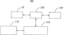
所述本体102进一步包括一壳体、一中央处理器、一存储单元及一控制单元。该中央处理器、存储单元、控制单元及显示屏104均设置于壳体内部。所述中央处理器、存储单元及控制单元可以集成设置于一集成电路板上。请参见图2,所述存储单元170及控制单元150分别通过集成电路板上的导线与所述中央处理器160电连接。所述显示屏104及触摸屏10分别与所述控制单元150电连接。所述控制单元150一般包括一触摸屏控制器、一显示屏控制器及多个功能控制器,分别控制触摸屏10、显示屏104及各种功能,如记事薄、辞典、通讯及遥控等所对应的功能控制器的工作。所述存储单元170用于存储中央处理器的控制操作所需的数据及操作结果。所述存储单元170可进一步包括一只读存储器,一随机存取存储器,及一可抹除可编程存储器。所述只读存储器用于储存系统软件的一些不会更动的资料。所述随机存取存储器用于储存对使用者所输入的资料进行处理后所获得的资料。所述个人数字助理100可进一步通过所述可抹除可编程存储器与一计算机进行数据交换。当需要将所述个人数字助理100中的信息输入计算机时,可通过中央处理器读取可抹除可编程存储器中所储存的系统软件,以处理相应的信息并传送至计算机。当需要通过计算机向个人数字助理100输入信息,可通过中央处理器读取可抹除可编程存储器中所储存的系统软件,以处理输入的信息,并传送至显示屏及/或随机存取存储器中。The
所述显示屏104为液晶显示屏、场发射显示屏、等离子显示屏、电致发光显示屏及真空荧光显示屏中的一种。该显示屏104用于显示本体102输出的数据和图像。优选地,所述的显示屏104为一液晶显示屏。The
所述触摸屏10可以与所述显示屏104间隔一预定距离设置,也可与所述显示屏104集成设置。具体地,当所述触摸屏10与所述显示屏104集成设置时,所述触摸屏10可通过粘结剂直接设置在显示屏104表面或所述触摸屏10可与所述显示屏104共用基板设置。所述触摸屏10具有输入信号的功能,用户可用手指或触摸笔等在触摸屏10上通过触摸或按压将信号输入给本体102。The
具体地,所述触摸屏10的面积可与显示屏104的面积相同。可以理解,根据使用需求,在显示屏104上可显示一屏幕键盘,从而可通过对触摸屏10的触摸达到按键效果。本技术方案实施例中,所述触摸屏10与所述显示屏104共用基板集成设置。所述触摸屏10可以为电阻式或电容式触摸屏10。Specifically, the area of the
请参阅图3及图4,本技术方案第一实施例的个人数字助理100中的触摸屏10为一电阻式触摸屏10,该电阻式触摸屏10包括一第一电极板12,一第二电极板14以及设置在第一电极板12与第二电极板14之间的多个透明的点状隔离物16。3 and 4, the
该电阻式触摸屏10的第一电极板12包括一第一基体120,一第一导电层122以及两个第一电极124。该第一基体120为平面结构,其具有一第一表面。该第一导电层122与两个第一电极124均设置在第一基体120的第一表面。两个第一电极124分别设置在第一导电层122沿第一方向的两端并与第一导电层122电连接。所述第一方向为X坐标方向。该触摸屏10的第二电极板14包括一第二基体140,一第二导电层142以及两个第二电极144。所述第二基体140为平面结构,且具有一第二表面。该第二基体140的第二表面与第一基体120的第一表面相对设置。该第二导电层142与两个第二电极144均设置在所述第二基体140第二表面。两个第二电极144分别设置在第二导电层142沿第二方向的两端并与第二导电层142电连接。所述第二方向为Y坐标方向。该X坐标方向垂直于Y坐标方向,即两个第一电极124与两个第二电极144正交设置。The first electrode plate 12 of the
其中,该第一基体120为透明的且具有一定柔软度的薄膜或薄板。该第二基体140为透明基板。该第二基体140的材料可选择为玻璃、石英、金刚石等硬性材料或塑料及树脂等柔性材料。所述第二基体140主要起支撑的作用。该第一电极124与该第二电极144的材料为金属、碳纳米管薄膜或其他导电材料,只要确保导电性即可。本实施例中,该第一基体120材料为聚酯膜,该第二基体140为玻璃基板;该第一电极124与第二电极144为碳纳米管薄膜,该碳纳米管薄膜的宽度均为1微米~5毫米。Wherein, the first substrate 120 is a transparent film or thin plate with a certain degree of flexibility. The
进一步地,该第二电极板14远离显示屏104的表面的外围设置有一绝缘层18。上述的第一电极板12设置在该绝缘层18上,且该第一电极板12的第一导电层122正对第二电极板14的第二导电层142设置。上述多个透明点状隔离物16设置在第二电极板14的第二导电层142上,且该多个透明点状隔离物16彼此间隔设置。第一电极板12与第二电极板14之间的距离为2~100微米。该绝缘层18与点状隔离物16均可采用绝缘透明树脂或其他绝缘透明材料制成。设置绝缘层18与点状隔离物16可使得第一电极板14与第二电极板12电绝缘。可以理解,当电阻式触摸屏10尺寸较小时,点状隔离物16为可选择的结构,只需确保第一电极板14与第二电极板12电绝缘即可。Further, an insulating
另外,该第一电极板12远离第二电极板14的表面可设置一透明保护膜126。所述透明保护膜126可以通过粘结剂直接粘结在第一基体120远离显示屏104的表面,也可采用热压法,与第一电极板压合在一起。该透明保护膜126可采用一层表面硬化处理、光滑防刮的塑料层或树脂层,该树脂层可由苯丙环丁烯(BCB)、聚甲基丙烯酸甲酯(PMMA)、聚酯、以及丙烯酸树脂等材料形成。本实施例中,形成该透明保护膜126的材料为聚对苯二甲酸乙二醇酯(PET),用于保护第一电极板12,提高耐用性。该透明保护膜126经特殊工艺处理后,可用以提供一些附加功能,如可以减少眩光或降低反射。In addition, a transparent
所述第一导电层122与第二导电层142中的至少一个导电层包括一碳纳米管层,该碳纳米管层包括多个均匀分布的碳纳米管,且上述的碳纳米管无序排列或有序排列。所述无序排列的碳纳米管通过范德华力相互缠绕、相互吸引且平行于碳纳米管层的表面。所述有序排列的碳纳米管沿一个方向或多个方向择优取向排列。At least one conductive layer in the first conductive layer 122 and the second conductive layer 142 includes a carbon nanotube layer, the carbon nanotube layer includes a plurality of uniformly distributed carbon nanotubes, and the above-mentioned carbon nanotubes are arranged in disorder or in order. The carbon nanotubes arranged in disorder are intertwined and attracted to each other by van der Waals force and are parallel to the surface of the carbon nanotube layer. The ordered carbon nanotubes are preferentially aligned along one direction or multiple directions.
不同结构的碳纳米管层可由不同的方法制备。所述有序排列的碳纳米管形成的有序碳纳米管层可由直接拉伸一碳纳米管阵列获得的有序碳纳米管薄膜组成。该有序碳纳米管薄膜中的碳纳米管首尾相连且沿拉伸方向择优取向排列,且相邻的碳纳米管之间通过范德华力紧密结合。所述有序碳纳米管薄膜进一步包括多个首尾相连的碳纳米管片段,每个碳纳米管片段具有大致相等的长度且每个碳纳米管片段由多个相互平行的碳纳米管构成,碳纳米管片段两端通过范德华力相互连接。所述碳纳米管薄膜的厚度为0.5纳米~100微米,宽度为0.01厘米~10厘米。所述有序碳纳米管层可进一步包括至少两个重叠设置的有序碳纳米管薄膜,相邻的两个有序碳纳米管薄膜中的碳纳米管具有一交叉角度α,且0度≤α≤90度。所述有序排列的碳纳米管形成的有序碳纳米管层也可通过碾压一碳纳米管阵列获得。所述碾压一碳纳米管阵列获得的有序碳纳米管层中的碳纳米管沿一个方向或多个方向择优取向排列。所述无序排列的碳纳米管形成的无序碳纳米管层可通过絮化处理一碳纳米管原料而获得。该无序碳纳米管层中的碳纳米管通过范德华力相互缠绕、吸引且平行于碳纳米管层的表面。Carbon nanotube layers with different structures can be prepared by different methods. The ordered carbon nanotube layer formed by the ordered carbon nanotubes can be composed of an ordered carbon nanotube film obtained by directly stretching a carbon nanotube array. The carbon nanotubes in the ordered carbon nanotube film are connected end to end and arranged in a preferred orientation along the stretching direction, and the adjacent carbon nanotubes are closely combined by van der Waals force. The ordered carbon nanotube film further includes a plurality of carbon nanotube segments connected end to end, each carbon nanotube segment has approximately equal length and each carbon nanotube segment is composed of a plurality of carbon nanotubes parallel to each other, carbon The two ends of the nanotube segments are connected to each other by van der Waals force. The carbon nanotube film has a thickness of 0.5 nanometers to 100 microns and a width of 0.01 centimeters to 10 centimeters. The ordered carbon nanotube layer may further include at least two ordered carbon nanotube films overlapping each other, the carbon nanotubes in two adjacent ordered carbon nanotube films have a crossing angle α, and 0 degree ≤ α≤90 degrees. The ordered carbon nanotube layer formed by the ordered carbon nanotubes can also be obtained by rolling a carbon nanotube array. The carbon nanotubes in the ordered carbon nanotube layer obtained by rolling a carbon nanotube array are preferentially aligned along one direction or multiple directions. The disordered carbon nanotube layer formed by the disorderly arranged carbon nanotubes can be obtained by flocculating a carbon nanotube raw material. The carbon nanotubes in the disordered carbon nanotube layer are intertwined and attracted to each other and parallel to the surface of the carbon nanotube layer through van der Waals force.
所述碳纳米管层中的碳纳米管包括单壁碳纳米管、双壁碳纳米管和多壁碳纳米管中的一种或多种。所述单壁碳纳米管的直径为0.5纳米~50纳米,双壁碳纳米管的直径为1纳米~50纳米,多壁碳纳米管的直径为1.5纳米~50纳米。The carbon nanotubes in the carbon nanotube layer include one or more of single-wall carbon nanotubes, double-wall carbon nanotubes and multi-wall carbon nanotubes. The single-walled carbon nanotubes have a diameter of 0.5 nm to 50 nm, the double-walled carbon nanotubes have a diameter of 1 nm to 50 nm, and the multi-walled carbon nanotubes have a diameter of 1.5 nm to 50 nm.
请参阅图5,本技术方案实施例中,所述第一导电层122与第二导电层142均包括一碳纳米管层,所述碳纳米管层为一有序碳纳米管薄膜,该碳纳米管薄膜中的碳纳米管首尾相连且沿拉伸方向择优取向排列。所述碳纳米管层为重叠设置的多层有序碳纳米管薄膜,每层碳纳米管薄膜中的碳纳米管沿同一方向择优取向排列。所述碳纳米管薄膜进一步包括多个首尾相连的碳纳米管片段,每个碳纳米管片段具有大致相等的长度且每个碳纳米管片段由多个相互平行的碳纳米管构成,碳纳米管片段两端通过范德华力相互连接。具体的,所述第一导电层122中的多层碳纳米管薄膜均沿第一方向重叠设置,第二导电层142中的多层碳纳米管薄膜均沿第二方向重叠设置。所述碳纳米管薄膜的厚度为0.5纳米~100微米,宽度为0.01厘米~10厘米。Please refer to Fig. 5, in the embodiment of this technical solution, the first conductive layer 122 and the second conductive layer 142 both include a carbon nanotube layer, and the carbon nanotube layer is an ordered carbon nanotube film, the carbon The carbon nanotubes in the nanotube film are connected end to end and arranged in a preferred orientation along the stretching direction. The carbon nanotube layer is a multi-layer ordered carbon nanotube film arranged overlappingly, and the carbon nanotubes in each layer of the carbon nanotube film are preferentially aligned along the same direction. The carbon nanotube film further includes a plurality of carbon nanotube segments connected end to end, each carbon nanotube segment has approximately equal length and each carbon nanotube segment is composed of a plurality of carbon nanotubes parallel to each other, the carbon nanotubes The ends of the fragments are connected to each other by van der Waals forces. Specifically, the multilayer carbon nanotube films in the first conductive layer 122 are all overlapped along the first direction, and the multilayer carbon nanotube films in the second conductive layer 142 are all overlapped along the second direction. The carbon nanotube film has a thickness of 0.5 nanometers to 100 microns and a width of 0.01 centimeters to 10 centimeters.
将所述触摸屏10与显示屏104集成设置时,为了进一步减小由显示设备产生的电磁干扰,避免从触摸屏10发出的信号产生错误,还可在触摸屏的下表面上设置一屏蔽层(图未示)。该屏蔽层可由铟锡氧化物(ITO)、锑锡氧化物(ATO)或碳纳米管薄膜等导电材料形成。作为屏蔽层的碳纳米管薄膜中的碳纳米管的排列方式不限,可为定向排列也可为其它的排列方式。本实施例中,该屏蔽层采用碳纳米管薄膜,其中的碳纳米管定向排列。该碳纳米管薄膜作为电接地点,起到屏蔽的作用,从而使得触摸屏10能在无干扰的环境中工作。When the
进一步地,为确保所述显示屏104不致于由于外力过大而损坏,可以在所述的显示屏104与触摸屏10之间设置一钝化层(图未示)。该钝化层可由氮化硅、氧化硅等材料形成。Further, in order to ensure that the
以下将具体介绍本实施例所述的个人数字助理100通过电阻式触摸屏10的触摸进行显示的具体过程。The specific process of displaying by the personal
请参阅图6,使用时,个人数字助理100的控制单元150在第一电极板12之间与第二电极板14之间分时施加5V电压。使用者一边视觉确认在触摸屏10下面设置的显示屏104的显示,一边通过触摸物180如手指或笔按压触摸屏10第一电极板12进行操作。第一电极板12中第一基体120发生弯曲,使得按压处182的第一导电层122与第二电极板14的第二导电层142接触形成导通。个人数字助理100的控制单元150中的触摸屏控制器分别测量第一导电层122X坐标方向上的电压变化与第二导电层142Y坐标方向上的电压变化,并进行精确计算,将它们转换成触点坐标,并将该数字化的触点坐标传递给中央处理器160。中央处理器160将该触点坐标对应的操作命令从个人数字助理100的存储器170中调出并传递给相应的控制单元150中的功能控制器,且控制所述功能控制器的处理操作,通过所述显示屏104显示所述功能控制器的处理结果。所述功能控制器根据操作命令控制显示屏104的显示。Please refer to FIG. 6 , when in use, the
请一并参阅图7至图9,本技术方案第二实施例提供一种个人数字助理200,具体包括一本体202及一触摸屏20。该本体202上设置有一显示屏204。所述触摸屏20设置于该显示屏204表面。Please refer to FIG. 7 to FIG. 9 together. The second embodiment of the technical solution provides a personal
本技术方案第二实施例个人数字助理200的结构与第一实施例个人数字助理100的结构相似,所不同的是,该触摸屏20为一电容式触摸屏20。该触摸屏20进一步包括一基体22、一透明导电层24、至少两个电极28及一透明保护膜26。该基板22靠近显示屏204设置。所述基体22具有一第一表面221以及与第一表面221相对的第二表面222。透明导电层24设置在基体22的第一表面221,该第一表面221为远离显示屏的一表面;上述至少两个电极28分别设置在透明导电层24的每个角处或边上,且与透明导电层24形成电连接,用以在透明导电层24上形成等电位面。透明保护膜26可直接设置在透明导电层24以及电极28上。The structure of the
具体地,可以采用四个电极28分别设置于透明导电层24的四个角或四条边上,用以在上述的透明导电层24上形成均匀的电阻网络。在本实施例中,四个带状电极28间隔设置在上述的透明导电层24同一表面的四个边上。可以理解,上述的电极28也可以设置在透明导电层24的不同表面上,其关键在于上述电极28的设置能使得在透明导电层24上形成等电位面即可。本实施例中,所述电极28设置在透明导电层24的远离基体22的一个表面上。Specifically, four
可以理解,所述的四个电极28亦可设置于透明导电层24与基体22之间,且与透明导电层24电连接。It can be understood that the four
所述基体22为一曲面型或平面型的结构。该基体22由玻璃、石英、金刚石或塑料等硬性材料或柔性材料形成。所述基体22主要起支撑的作用。The
所述透明导电层24包括一碳纳米管层,该碳纳米管层包括多个均匀分布的碳纳米管,且上述的碳纳米管无序排列或有序排列。具体地,所述碳纳米管层的结构可以与第一实施例中第一导电层122或第二导电层142中的碳纳米管层结构相同。The transparent
所述四个电极28的材料为金属、碳纳米管薄膜或其他导电材料,只要确保导电性即可。本实施例中,所述四个电极28为由银或铜等低电阻的导电金属镀层或者金属箔片组成的条状电极28。The materials of the four
进一步地,为了延长透明导电层24的使用寿命和限制耦合在接触点与透明导电层24之间的电容,可以在透明导电层24和电极28远离基体22的表面设置一透明的透明保护膜26,透明保护膜26可由氮化硅、氧化硅、苯丙环丁烯(BCB)、聚酯膜或丙烯酸树脂等形成。该透明保护膜26具有一定的硬度,对透明导电层24起保护作用。可以理解,还可通过特殊的工艺处理,从而使得透明保护膜26具有以下功能,例如减小炫光、降低反射等。Further, in order to prolong the service life of the transparent
在本实施例中,在形成有电极28的透明导电层24上设置一二氧化硅层用作透明保护膜26,该透明保护膜26的硬度可达到7H(H为洛氏硬度试验中,卸除主试验力后,在初试验力下压痕残留的深度)。可以理解,透明保护膜26的硬度和厚度可以根据需要进行选择。所述透明保护膜26可以通过粘结剂直接粘结在透明导电层24远离显示屏204的表面。In this embodiment, on the transparent
此外,可选择地,为了减小由显示设备产生的电磁干扰,避免从触摸屏20发出的信号产生错误,还可在基体22的第二表面222上设置一屏蔽层230。该屏蔽层230可由铟锡氧化物(ITO)薄膜、锑锡氧化物(ATO)薄膜或碳纳米管薄膜等透明导电材料形成。该碳纳米管薄膜可以是定向排列的或其它结构的碳纳米管薄膜。本实施例中,该碳纳米管薄膜包括多个碳纳米管,所述多个碳纳米管在上述的碳纳米管薄膜中定向排列,其具体结构可与所述透明导电层24相同。该碳纳米管薄膜作为电接地点,起到屏蔽的作用,从而使得触摸屏20能在无干扰的环境中工作。进一步地,为使所述显示屏204不致于由于外力过大而损坏,可以于所述的显示屏204与屏蔽层230之间设置一钝化层232。该钝化层232可由氮化硅、氧化硅等材料形成。In addition, optionally, in order to reduce electromagnetic interference generated by the display device and avoid errors in signals sent from the touch screen 20 , a shielding layer 230 may also be provided on the
以下将具体介绍本实施例所述的个人数字助理200通过电容式触摸屏20的触摸进行显示的具体过程。The specific process of displaying by the personal
在使用时,个人数字助理200的控制单元250在透明导电层24上施加一预定电压。电压通过电极28施加到透明导电层24上,从而在该透明导电层24上形成等电位面。使用者一边视觉确认在触摸屏20后面设置的显示屏204的显示,一边通过手指或笔等触摸物按压或接近触摸屏20的透明保护膜26进行操作时,触摸物与透明导电层24之间形成一耦合电容。对于高频电流来说,电容是直接导体,于是手指从接触点吸走了一部分电流。这个电流分别从触摸屏20上的电极28中流出,并且流经这四个电极28的电流与手指到四角的距离成正比,控制单元250通过对这四个电流比例的精确计算,得出触摸点的位置。之后,控制单元250将数字化的触摸位置数据传送给中央处理器260。然后,中央处理器260接受上述的触摸位置数据,并将该触点坐标对应的操作命令从个人数字助理200的存储单元270中调出并传递给相应的控制单元250。控制单元250根据操作命令控制显示屏204的显示以及各种功能的工作。In use, the
本技术方案实施例提供的采用碳纳米管层作为透明导电层的个人数字助理具有以下优点:其一,由于碳纳米管层在潮湿的条件下具有良好的透明度,故采用碳纳米管层作为触摸屏的透明导电层,可以使应用该触摸屏的个人数字助理具有较好的透明度;其二,由于碳纳米管具有优异的力学性能,则由碳纳米管组成的碳纳米管层具有较好的韧性及机械强度,故采用该碳纳米管层作为触摸屏的透明导电层,可以相应的提高触摸屏的耐用性,进而提高使用该触摸屏的个人数字助理的耐用性;其三,由于碳纳米管具有优异的导电性能,则由碳纳米管组成的碳纳米管层具有均匀的阻值分布,因而,采用上述碳纳米管层作透明导电层,可以相应的提高触摸屏的分辨率和精确度,进而提高应用该触摸屏的个人数字助理的分辨率和精确度。The personal digital assistant using the carbon nanotube layer as the transparent conductive layer provided by the embodiment of the technical solution has the following advantages: First, because the carbon nanotube layer has good transparency under humid conditions, the carbon nanotube layer is used as the touch screen The transparent conductive layer can make the personal digital assistant using the touch screen have better transparency; second, because carbon nanotubes have excellent mechanical properties, the carbon nanotube layer composed of carbon nanotubes has better toughness and Mechanical strength, so using the carbon nanotube layer as the transparent conductive layer of the touch screen can correspondingly improve the durability of the touch screen, and then improve the durability of the personal digital assistant using the touch screen; third, because the carbon nanotube has excellent conductivity Performance, the carbon nanotube layer composed of carbon nanotubes has a uniform resistance distribution, therefore, using the above-mentioned carbon nanotube layer as a transparent conductive layer can correspondingly improve the resolution and accuracy of the touch screen, and then improve the application of the touch screen. The resolution and precision of a personal digital assistant.
另外,本领域技术人员还可在本发明精神内作其它变化,当然这些依据本发明精神所作的变化,都应包含在本发明所要求保护的范围内。In addition, those skilled in the art can also make other changes within the spirit of the present invention. Of course, these changes made according to the spirit of the present invention should be included in the scope of protection claimed by the present invention.
Claims (16)
Priority Applications (7)
| Application Number | Priority Date | Filing Date | Title |
|---|---|---|---|
| CN2008101420230ACN101655720B (en) | 2008-08-22 | 2008-08-22 | Personal digital assistant |
| EP08253439AEP2053495A3 (en) | 2007-10-23 | 2008-10-22 | Touch panel, method for making the same, and display device adopting the same |
| EP08253437AEP2053496A3 (en) | 2007-10-23 | 2008-10-22 | Touch panel and display device adopting the same |
| KR1020080104437AKR101210701B1 (en) | 2007-10-23 | 2008-10-23 | Touch panel, method for making the same, and electronic device adopting the same |
| KR1020080104457AKR101212421B1 (en) | 2007-10-23 | 2008-10-23 | Touch panel, method for making the same, and electronic device adopting the same |
| US12/384,328US8346316B2 (en) | 2008-08-22 | 2009-04-02 | Personal digital assistant |
| JP2009193178AJP2010049691A (en) | 2008-08-22 | 2009-08-24 | Personal digital assistant |
Applications Claiming Priority (1)
| Application Number | Priority Date | Filing Date | Title |
|---|---|---|---|
| CN2008101420230ACN101655720B (en) | 2008-08-22 | 2008-08-22 | Personal digital assistant |
Publications (2)
| Publication Number | Publication Date |
|---|---|
| CN101655720A CN101655720A (en) | 2010-02-24 |
| CN101655720Btrue CN101655720B (en) | 2012-07-18 |
Family
ID=41696870
Family Applications (1)
| Application Number | Title | Priority Date | Filing Date |
|---|---|---|---|
| CN2008101420230AExpired - Fee RelatedCN101655720B (en) | 2007-10-23 | 2008-08-22 | Personal digital assistant |
Country Status (3)
| Country | Link |
|---|---|
| US (1) | US8346316B2 (en) |
| JP (1) | JP2010049691A (en) |
| CN (1) | CN101655720B (en) |
Families Citing this family (17)
| Publication number | Priority date | Publication date | Assignee | Title |
|---|---|---|---|---|
| US8390580B2 (en)* | 2008-07-09 | 2013-03-05 | Tsinghua University | Touch panel, liquid crystal display screen using the same, and methods for making the touch panel and the liquid crystal display screen |
| CN101924816B (en)* | 2009-06-12 | 2013-03-20 | 清华大学 | Flexible mobile phone |
| JP2011017626A (en)* | 2009-07-09 | 2011-01-27 | Sony Corp | Mechanical quantity detection member and mechanical quantity detection apparatus |
| USD641332S1 (en)* | 2010-01-06 | 2011-07-12 | Sony Ericsson Mobile Communications Ab | Mobile phone |
| CN101880035A (en) | 2010-06-29 | 2010-11-10 | 清华大学 | carbon nanotube structure |
| USD687024S1 (en)* | 2010-07-06 | 2013-07-30 | Sony Corporation | Information terminal |
| FR2963445B1 (en)* | 2010-08-02 | 2013-05-03 | Nanomade Concept | TOUCH SURFACE AND METHOD FOR MANUFACTURING SUCH SURFACE |
| USD645437S1 (en)* | 2010-11-16 | 2011-09-20 | Cheng Uei Precision Industry Co., Ltd. | Mobile phone |
| KR101330809B1 (en)* | 2011-08-03 | 2013-12-19 | 주식회사 팬택 | Touch panel and electronic device including the touch panel |
| TWI581135B (en)* | 2011-09-30 | 2017-05-01 | 加拿都公司 | Touch sensitive film, touch sensing device, and electronic device |
| CN103576356A (en)* | 2012-07-23 | 2014-02-12 | 天津富纳源创科技有限公司 | Production method for liquid crystal module having touch function |
| CN103576351A (en)* | 2012-07-23 | 2014-02-12 | 天津富纳源创科技有限公司 | Liquid crystal module having touch function |
| CN103576352A (en)* | 2012-07-23 | 2014-02-12 | 天津富纳源创科技有限公司 | LCD (Liquid Crystal Display) module with touch function |
| USD716796S1 (en)* | 2012-12-12 | 2014-11-04 | Americhip, Inc. | Video tablet |
| USD756355S1 (en)* | 2013-11-20 | 2016-05-17 | Fujifilm Corporation | Personal digital assistance |
| USD756354S1 (en)* | 2013-11-20 | 2016-05-17 | Fujifilm Corporation | Personal digital assistance |
| WO2018051708A1 (en)* | 2016-09-13 | 2018-03-22 | コニカミノルタ株式会社 | Illuminating device |
Citations (5)
| Publication number | Priority date | Publication date | Assignee | Title |
|---|---|---|---|---|
| CN1447279A (en)* | 2003-03-18 | 2003-10-08 | 中国电子科技集团公司第五十五研究所 | High reliable touch screen and manufacturing technique |
| CN1467544A (en)* | 2002-07-02 | 2004-01-14 | ���ǵ�����ʽ���� | LCD components for personal digital assistants |
| CN1483667A (en)* | 2002-09-16 | 2004-03-24 | �廪��ѧ | A carbon nanotube rope and its manufacturing method |
| CN2638143Y (en)* | 2003-05-24 | 2004-09-01 | 江阴市华丽计算机网络工程有限公司 | Multifunctional PDA |
| CN101059738A (en)* | 2006-04-20 | 2007-10-24 | 铼宝科技股份有限公司 | Transparent touch screen with upward-emitting organic light-emitting diodes |
Family Cites Families (174)
| Publication number | Priority date | Publication date | Assignee | Title |
|---|---|---|---|---|
| JPS61231626A (en) | 1985-04-05 | 1986-10-15 | Asahi Chem Ind Co Ltd | Conductive sheet for position detection |
| US4659873A (en) | 1985-07-19 | 1987-04-21 | Elographics, Inc. | Fabric touch sensor and method of manufacture |
| JPH0350177Y2 (en) | 1985-10-11 | 1991-10-25 | ||
| JPS62182916U (en) | 1986-05-08 | 1987-11-20 | ||
| JPH0344004Y2 (en) | 1986-05-26 | 1991-09-17 | ||
| US4853498A (en) | 1988-06-13 | 1989-08-01 | Tektronix, Inc. | Position measurement apparatus for capacitive touch panel system |
| US4933660A (en) | 1989-10-27 | 1990-06-12 | Elographics, Inc. | Touch sensor with touch pressure capability |
| EP0435438B1 (en) | 1989-12-28 | 1998-03-04 | Gunze Limited | Input system including resistance film touch panel |
| JPH0628090Y2 (en) | 1992-06-03 | 1994-08-03 | 健一 古谷 | Electrode structure in used needle processing equipment |
| US5861583A (en) | 1992-06-08 | 1999-01-19 | Synaptics, Incorporated | Object position detector |
| JPH06339252A (en) | 1993-05-27 | 1994-12-06 | Mabuchi Motor Co Ltd | Rotation detecting device for small dc motor |
| TW242732B (en) | 1993-06-29 | 1995-03-11 | Victor Company Of Japan | Digital chrominance signal processing circuit |
| JPH08222893A (en) | 1995-02-17 | 1996-08-30 | Japan Tobacco Inc | Workpiece mounting machine suction nozzle |
| US6373472B1 (en) | 1995-10-13 | 2002-04-16 | Silviu Palalau | Driver control interface system |
| US5853877A (en) | 1996-05-31 | 1998-12-29 | Hyperion Catalysis International, Inc. | Method for disentangling hollow carbon microfibers, electrically conductive transparent carbon microfibers aggregation film amd coating for forming such film |
| TW341684B (en) | 1996-07-15 | 1998-10-01 | Synaptics Inc | Object position detector |
| JP3861333B2 (en) | 1996-08-27 | 2006-12-20 | 松下電器産業株式会社 | Coordinate position input device |
| US7663607B2 (en) | 2004-05-06 | 2010-02-16 | Apple Inc. | Multipoint touchscreen |
| JP3309851B2 (en) | 1998-05-15 | 2002-07-29 | 東洋紡績株式会社 | Transparent conductive film and touch panel |
| US5931764A (en) | 1998-06-24 | 1999-08-03 | Viztec, Inc. | Wearable device with flexible display |
| US6664950B1 (en) | 1999-11-17 | 2003-12-16 | L-3 Communications | Resistive touch panel using removable, tensioned top layer |
| JP2001222378A (en) | 2000-02-10 | 2001-08-17 | Nec Saitama Ltd | Touch panel input device |
| JP2001267782A (en) | 2000-03-21 | 2001-09-28 | Shimadzu Corp | Electromagnetic wave absorption shielding material |
| TW521227B (en) | 2000-03-31 | 2003-02-21 | Sharp Kk | Electrode substrate, method for producing the same and display device including the same |
| KR100698898B1 (en) | 2000-08-03 | 2007-03-22 | 한국터치스크린(주) | Touch panel |
| US6423583B1 (en) | 2001-01-03 | 2002-07-23 | International Business Machines Corporation | Methodology for electrically induced selective breakdown of nanotubes |
| TW521259B (en) | 2001-01-11 | 2003-02-21 | Atouch Co Ltd | Flat panel display with input device |
| JP2002278701A (en) | 2001-03-21 | 2002-09-27 | Nissha Printing Co Ltd | Touch panel |
| WO2002076724A1 (en) | 2001-03-26 | 2002-10-03 | Eikos, Inc. | Coatings containing carbon nanotubes |
| TW508652B (en) | 2001-10-03 | 2002-11-01 | Taiwan Semiconductor Mfg | Device and method for wafer drying |
| JP3798287B2 (en) | 2001-10-10 | 2006-07-19 | Smk株式会社 | Touch panel input device |
| KR20030055856A (en) | 2001-12-27 | 2003-07-04 | 엘지.필립스 엘시디 주식회사 | Fabricated Method Of Liquid Crystal Display Apparatus Integrated Film Type Touch Panel |
| KR100840670B1 (en) | 2001-12-27 | 2008-06-24 | 엘지디스플레이 주식회사 | Touch panel integrated liquid crystal display panel |
| KR100796489B1 (en) | 2001-12-28 | 2008-01-21 | 엘지.필립스 엘시디 주식회사 | Touch panel device and manufacturing method thereof |
| JP4051988B2 (en) | 2002-04-09 | 2008-02-27 | 富士ゼロックス株式会社 | Photoelectric conversion element and photoelectric conversion device |
| CN2539375Y (en) | 2002-04-15 | 2003-03-05 | 湖南三才光电信息材料有限公司 | High-stable flexible transparent conducting composite film |
| AU2003229333A1 (en) | 2002-05-21 | 2003-12-12 | Eikos, Inc. | Method for patterning carbon nanotube coating and carbon nanotube wiring |
| US7405774B2 (en) | 2002-08-20 | 2008-07-29 | Samsung Electronics Co., Ltd. | Light guide plate and liquid crystal display having the same |
| CN1281982C (en) | 2002-09-10 | 2006-10-25 | 清华大学 | Polarized element and method for manufacturing same |
| KR100459230B1 (en) | 2002-11-14 | 2004-12-03 | 엘지.필립스 엘시디 주식회사 | touch panel for display device |
| KR100451773B1 (en) | 2002-11-20 | 2004-10-08 | 엘지.필립스 엘시디 주식회사 | Touch Panel in Digital Resistive Type |
| JP2004189573A (en) | 2002-12-13 | 2004-07-08 | Jfe Engineering Kk | Aggregate of carbon nanotubes and carbon nanotube installation device having the same |
| CN1286715C (en) | 2002-12-21 | 2006-11-29 | 清华大学 | Carbon nanometer tube array structure and growing method thereof |
| KR100685954B1 (en) | 2002-12-24 | 2007-02-23 | 엘지.필립스 엘시디 주식회사 | Touch panel |
| CN1321885C (en) | 2003-01-23 | 2007-06-20 | 南昌大学 | Method for preparing film of tube of directed nano carbon on soft base |
| JP2004230690A (en) | 2003-01-30 | 2004-08-19 | Takiron Co Ltd | Antistatic transparent resin sheet |
| JP2007112133A (en) | 2003-01-30 | 2007-05-10 | Takiron Co Ltd | Electroconductive shaped article |
| JP4471346B2 (en) | 2003-01-31 | 2010-06-02 | タキロン株式会社 | Electromagnetic shield |
| JP4572543B2 (en) | 2003-02-14 | 2010-11-04 | 東レ株式会社 | Field effect transistor and liquid crystal display device using the same |
| KR100509763B1 (en) | 2003-03-11 | 2005-08-25 | 엘지전자 주식회사 | Front filter of plasma display panel |
| US7150865B2 (en) | 2003-03-31 | 2006-12-19 | Honda Giken Kogyo Kabushiki Kaisha | Method for selective enrichment of carbon nanotubes |
| JP4586334B2 (en) | 2003-05-07 | 2010-11-24 | ソニー株式会社 | Field effect transistor and manufacturing method thereof |
| GB0313808D0 (en) | 2003-06-14 | 2003-07-23 | Binstead Ronald P | Improvements in touch technology |
| JP2005037851A (en) | 2003-06-24 | 2005-02-10 | Seiko Epson Corp | Electrophoretic dispersion liquid, electrophoretic display device, electrophoretic display device manufacturing method, and electronic apparatus |
| CN1315362C (en) | 2003-06-27 | 2007-05-09 | 中国科学院上海硅酸盐研究所 | Carbon nano-pipe/ceramic composite material possessing microwave absorption function and its preparation method |
| JP2005028821A (en)* | 2003-07-10 | 2005-02-03 | Sony Corp | Transparent conductive base and touch panel |
| JP4325479B2 (en) | 2003-07-17 | 2009-09-02 | セイコーエプソン株式会社 | Organic transistor manufacturing method, active matrix device manufacturing method, display device manufacturing method, and electronic device manufacturing method |
| TWI249134B (en) | 2003-07-23 | 2006-02-11 | Wintek Corp | Touch panel structure |
| JP2005056604A (en) | 2003-08-06 | 2005-03-03 | Hitachi Displays Ltd | Self-luminous flat panel display |
| JP4415653B2 (en) | 2003-11-19 | 2010-02-17 | セイコーエプソン株式会社 | Thin film transistor manufacturing method |
| JP4804711B2 (en) | 2003-11-21 | 2011-11-02 | 株式会社 日立ディスプレイズ | Image display device |
| JP4038685B2 (en) | 2003-12-08 | 2008-01-30 | 独立行政法人科学技術振興機構 | Actuator element |
| US20050209392A1 (en) | 2003-12-17 | 2005-09-22 | Jiazhong Luo | Polymer binders for flexible and transparent conductive coatings containing carbon nanotubes |
| JP2005182339A (en) | 2003-12-18 | 2005-07-07 | Kawaguchiko Seimitsu Co Ltd | Touch panel and screen input type display device therewith |
| JP4336592B2 (en) | 2004-02-04 | 2009-09-30 | シチズンホールディングス株式会社 | Position input device |
| JP2005286158A (en) | 2004-03-30 | 2005-10-13 | Seiko Epson Corp | PATTERN FORMING METHOD, ELECTRONIC DEVICE, ITS MANUFACTURING METHOD, AND ELECTRONIC DEVICE |
| CN1960943B (en) | 2004-04-19 | 2013-01-02 | 独立行政法人科学技术振兴机构 | Carbon-based fine structure group, aggregate of carbon based fine structure, use thereof and method for preparation thereof |
| WO2005104141A1 (en) | 2004-04-20 | 2005-11-03 | Takiron Co., Ltd. | Touch panel-use transparent conductive molded product and touch panel |
| CN1690915A (en) | 2004-04-28 | 2005-11-02 | 秦建忠 | Double screen notebook computer |
| TWI261716B (en) | 2004-05-13 | 2006-09-11 | Quanta Display Inc | Liquid crystal display apparatus and fabrication thereof |
| JP2008500933A (en) | 2004-05-14 | 2008-01-17 | ソニー ドイチュラント ゲゼルシャフト ミット ベシュレンクテル ハフツング | Composite material comprising carbon nanotube and metal carbonate |
| CN2706973Y (en) | 2004-06-30 | 2005-06-29 | 陈凯 | Fingers-nipping gloves cell phone |
| CN1998067B (en) | 2004-07-06 | 2010-07-14 | 毫微-专卖股份有限公司 | Activation of carbon nanotubes in field emission applications |
| ES2555309T3 (en) | 2004-07-06 | 2015-12-30 | Maricare Oy | Sensor product for electric field detection |
| US7194912B2 (en) | 2004-07-13 | 2007-03-27 | United States Of America As Represented By The Administrator Of The National Aeronautics And Space Administration | Carbon nanotube-based sensor and method for continually sensing changes in a structure |
| US7129097B2 (en) | 2004-07-29 | 2006-10-31 | International Business Machines Corporation | Integrated circuit chip utilizing oriented carbon nanotube conductive layers |
| JP4539241B2 (en) | 2004-09-02 | 2010-09-08 | パナソニック株式会社 | Touch panel and manufacturing method thereof |
| TWI249708B (en) | 2004-09-09 | 2006-02-21 | Ind Tech Res Inst | Analog resistive touch panel without bias |
| US7345296B2 (en) | 2004-09-16 | 2008-03-18 | Atomate Corporation | Nanotube transistor and rectifying devices |
| US20070298253A1 (en) | 2004-09-17 | 2007-12-27 | Kenji Hata | Transparent Conductive Carbon Nanotube Film and a Method for Producing the Same |
| US7573547B2 (en)* | 2004-09-27 | 2009-08-11 | Idc, Llc | System and method for protecting micro-structure of display array using spacers in gap within display device |
| JP2006171336A (en) | 2004-12-15 | 2006-06-29 | Takiron Co Ltd | Transparent electrode member for image display, and the image display device |
| TWI339290B (en) | 2004-12-31 | 2011-03-21 | Hon Hai Prec Ind Co Ltd | Liquid crystal display device |
| US8223444B2 (en) | 2005-01-07 | 2012-07-17 | Olympus Corporation | Medium exhibiting negative refraction, optical element, and optical system |
| US20060262055A1 (en) | 2005-01-26 | 2006-11-23 | Toshiba Matsushita Display Technology | Plane display device |
| TWI258708B (en) | 2005-01-27 | 2006-07-21 | Apex Material Technology Corp | Resistive touch panel, and it manufacturing method |
| JP5028744B2 (en) | 2005-02-15 | 2012-09-19 | 富士通株式会社 | Method for forming carbon nanotube and method for manufacturing electronic device |
| TWI267014B (en) | 2005-02-21 | 2006-11-21 | Au Optronics Corp | Organic light emitting diode display |
| US20060188721A1 (en) | 2005-02-22 | 2006-08-24 | Eastman Kodak Company | Adhesive transfer method of carbon nanotube layer |
| JP4679182B2 (en) | 2005-03-04 | 2011-04-27 | 株式会社シーズ・ラボ | Map display method, map display program, and map display device |
| US20060213251A1 (en) | 2005-03-24 | 2006-09-28 | University Of Florida Research Foundation, Inc. | Carbon nanotube films for hydrogen sensing |
| JP2006269311A (en) | 2005-03-25 | 2006-10-05 | Toray Ind Inc | Transparent conductive film containing carbon nano-tube obtained by making metal-carrying carrier contact with carbon-containing organic compound |
| TWI253846B (en) | 2005-03-28 | 2006-04-21 | Ind Tech Res Inst | Photo-sensing display unit |
| JP2006285068A (en) | 2005-04-04 | 2006-10-19 | Nikkiso Co Ltd | Conductive polarizing film |
| KR100770258B1 (en) | 2005-04-22 | 2007-10-25 | 삼성에스디아이 주식회사 | Organic thin film transistor and its manufacturing method |
| JP2006310154A (en) | 2005-04-28 | 2006-11-09 | Bussan Nanotech Research Institute Inc | Transparent conductive film and coating composition for transparent conductive film |
| JP5288441B2 (en) | 2005-05-10 | 2013-09-11 | 住友精密工業株式会社 | High thermal conductive composite material and its manufacturing method |
| US7633583B2 (en) | 2005-05-23 | 2009-12-15 | Ran-Hong Raymond Wang | Controlling polarization for liquid crystal displays |
| DE102006023993A1 (en) | 2005-05-23 | 2007-03-08 | Wang, Ran-Hong, Tustin | Polarization control for liquid crystal displays |
| EP1892609A4 (en) | 2005-05-26 | 2013-03-27 | Gunze Kk | Transparent planar body and transparent touch switch |
| US7645497B2 (en) | 2005-06-02 | 2010-01-12 | Eastman Kodak Company | Multi-layer conductor with carbon nanotubes |
| US7535462B2 (en) | 2005-06-02 | 2009-05-19 | Eastman Kodak Company | Touchscreen with one carbon nanotube conductive layer |
| US7593004B2 (en)* | 2005-06-02 | 2009-09-22 | Eastman Kodak Company | Touchscreen with conductive layer comprising carbon nanotubes |
| US8545790B2 (en) | 2005-06-04 | 2013-10-01 | Gregory Konesky | Cross-linked carbon nanotubes |
| WO2006132254A1 (en) | 2005-06-07 | 2006-12-14 | Kuraray Co., Ltd. | Carbon nanotube dispersion liquid and transparent conductive film using same |
| JP2008210528A (en) | 2005-06-16 | 2008-09-11 | Nissha Printing Co Ltd | Casing with illuminated switch and its manufacturing method |
| JP2007011997A (en)* | 2005-07-04 | 2007-01-18 | Fujitsu Component Ltd | Touch panel |
| JP2007018226A (en) | 2005-07-07 | 2007-01-25 | Three M Innovative Properties Co | Touch panel sensor |
| WO2007012899A1 (en) | 2005-07-25 | 2007-02-01 | Plastic Logic Limited | Flexible touch screen display |
| CN1903793A (en) | 2005-07-26 | 2007-01-31 | 中国科学院物理研究所 | Carbon silicon composite material, its preparation method and use |
| EP2477230B1 (en) | 2005-08-12 | 2015-02-25 | Cambrios Technologies Corporation | Nanowires-based transparent conductors on a flexible donor substrate |
| CN100336192C (en) | 2005-08-18 | 2007-09-05 | 上海交通大学 | Method for bonding nanometer material on metal electrode |
| JP2007123870A (en) | 2005-09-29 | 2007-05-17 | Matsushita Electric Ind Co Ltd | Flat panel display device and manufacturing method thereof |
| CN100543905C (en) | 2005-09-30 | 2009-09-23 | 北京富纳特创新科技有限公司 | A field emission device and its preparation method |
| US7995777B2 (en) | 2005-10-03 | 2011-08-09 | Xun Yu | Thin film transparent acoustic transducer |
| US20070085838A1 (en) | 2005-10-17 | 2007-04-19 | Ricks Theodore K | Method for making a display with integrated touchscreen |
| CN100412654C (en) | 2005-10-27 | 2008-08-20 | 清华大学 | Liquid crystal display device and manufacturing method thereof |
| TWI297088B (en) | 2005-10-28 | 2008-05-21 | Hon Hai Prec Ind Co Ltd | Liquid crystal display and its manufacturing method |
| CN100427388C (en) | 2005-11-25 | 2008-10-22 | 清华大学 | A large-area ultra-thin carbon nanotube film and its preparation process |
| CN101317205B (en) | 2005-11-29 | 2010-11-03 | 精工电子有限公司 | Process for producing display and method of laminating |
| TWI386420B (en) | 2005-12-06 | 2013-02-21 | Mitsubishi Rayon Co | Carbon nanotube structure, composite and manufacturing method thereof |
| JP4908136B2 (en) | 2005-12-06 | 2012-04-04 | 三菱レイヨン株式会社 | Carbon nanotube-containing composition, composite, and production method thereof |
| TW200722559A (en) | 2005-12-06 | 2007-06-16 | Ind Tech Res Inst | Metal nanodot arrays and fabrication methods thereof |
| CN2844974Y (en) | 2005-12-08 | 2006-12-06 | 比亚迪股份有限公司 | Contact style liquid crystal display device |
| CN100462301C (en) | 2005-12-09 | 2009-02-18 | 清华大学 | A kind of preparation method of carbon nanotube array |
| CN100500556C (en) | 2005-12-16 | 2009-06-17 | 清华大学 | Carbon nanotube filament and method for making the same |
| US8264137B2 (en) | 2006-01-03 | 2012-09-11 | Samsung Electronics Co., Ltd. | Curing binder material for carbon nanotube electron emission cathodes |
| TW200727163A (en) | 2006-01-06 | 2007-07-16 | Pan Jit Internat Inc | Antibacterial touch display device |
| JP5050352B2 (en) | 2006-01-10 | 2012-10-17 | Nok株式会社 | Post-treatment method for carbon material thin film |
| US8421755B2 (en) | 2006-01-17 | 2013-04-16 | World Properties, Inc. | Capacitive touch sensor with integral EL backlight |
| JP4779681B2 (en) | 2006-02-07 | 2011-09-28 | パナソニック株式会社 | Touch panel |
| KR20070081902A (en) | 2006-02-14 | 2007-08-20 | 삼성전자주식회사 | Liquid crystal display |
| JP4968854B2 (en) | 2006-02-28 | 2012-07-04 | 東洋紡績株式会社 | Carbon nanotube aggregate, carbon nanotube fiber, and method for producing carbon nanotube fiber |
| JP2007229989A (en) | 2006-02-28 | 2007-09-13 | Takiron Co Ltd | Conductive molded body and its manufacturing method |
| TWM306694U (en) | 2006-03-15 | 2007-02-21 | Ushine Photonics Corp | Durable resistive touch screen |
| TWI308290B (en) | 2006-03-17 | 2009-04-01 | Innolux Display Corp | Touch panel |
| TWI331374B (en) | 2006-03-23 | 2010-10-01 | Unimicron Technology Corp | Carbon nanotube field emitting display |
| JP4799237B2 (en)* | 2006-03-27 | 2011-10-26 | 三洋電機株式会社 | Displacement detection sensor, displacement detection device, and terminal device |
| US20090056854A1 (en) | 2006-04-04 | 2009-03-05 | Top-Nanosis, Inc. | Method for manufacturing conductive composite material |
| JP2007310869A (en) | 2006-04-17 | 2007-11-29 | Matsushita Electric Ind Co Ltd | Input device control method and input device used therefor |
| GB2437827B (en) | 2006-05-05 | 2008-03-26 | Harald Philipp | Touch screen element |
| KR20070113763A (en)* | 2006-05-26 | 2007-11-29 | 삼성전자주식회사 | Carbon nanotube pattern forming method and carbon nanotube pattern obtained thereby |
| US7796123B1 (en) | 2006-06-20 | 2010-09-14 | Eastman Kodak Company | Touchscreen with carbon nanotube conductive layers |
| US7630041B2 (en) | 2006-06-23 | 2009-12-08 | Tsinghua University | Liquid crystal cell assembly for liquid crystal display |
| US20080048996A1 (en) | 2006-08-11 | 2008-02-28 | Unidym, Inc. | Touch screen devices employing nanostructure networks |
| KR20060129977A (en) | 2006-09-08 | 2006-12-18 | 아이티엠 주식회사 | Highly durable resistive touch screen panel and its manufacturing method |
| KR100790216B1 (en) | 2006-10-17 | 2008-01-02 | 삼성전자주식회사 | CNC Transparent Electrode Using Conductive Dispersant and Manufacturing Method Thereof |
| CN100450922C (en) | 2006-11-10 | 2009-01-14 | 清华大学 | Ultralong orientational carbon nano-tube filament/film and its preparation method |
| JP4350740B2 (en) | 2006-12-05 | 2009-10-21 | レノボ・シンガポール・プライベート・リミテッド | Portable electronic device, method for changing display direction of screen, program, and storage medium |
| CN100405617C (en) | 2006-12-29 | 2008-07-23 | 清华大学 | Solar cell based on carbon nanotube film and preparation method thereof |
| US20080192014A1 (en) | 2007-02-08 | 2008-08-14 | Tyco Electronics Corporation | Touch screen using carbon nanotube electrodes |
| CN101239712B (en) | 2007-02-09 | 2010-05-26 | 清华大学 | Carbon nanotube film structure and preparation method thereof |
| WO2008127780A2 (en)* | 2007-02-21 | 2008-10-23 | Nantero, Inc. | Symmetric touch screen system with carbon nanotube-based transparent conductive electrode pairs |
| CN101276012B (en) | 2007-03-30 | 2016-04-27 | 清华大学 | Polarizing element and its preparation method |
| CN101280161B (en) | 2007-04-06 | 2013-01-09 | 清华大学 | Conducting adhesive tape and manufacturing method thereof |
| US20080266273A1 (en) | 2007-04-24 | 2008-10-30 | White Electronic Designs Corp. | Interactive display system |
| KR20090023803A (en) | 2007-09-03 | 2009-03-06 | 삼성전자주식회사 | Liquid crystal display panel and manufacturing method thereof |
| CN101419519B (en) | 2007-10-23 | 2012-06-20 | 清华大学 | Touch panel |
| CN101458597B (en) | 2007-12-14 | 2011-06-08 | 清华大学 | Touch screen, method for producing the touch screen, and display device using the touch screen |
| CN101419518B (en) | 2007-10-23 | 2012-06-20 | 清华大学 | Touch panel |
| CN101458594B (en) | 2007-12-12 | 2012-07-18 | 清华大学 | Touch screen and display device |
| CN101620454A (en) | 2008-07-04 | 2010-01-06 | 清华大学 | Potable computer |
| CN101458606B (en) | 2007-12-12 | 2012-06-20 | 清华大学 | Touch screen, method for producing the touch screen, and display device using the touch screen |
| TWI357167B (en) | 2007-12-21 | 2012-01-21 | Hon Hai Prec Ind Co Ltd | Touch panel, method for making the same, and displ |
| CN101470565B (en) | 2007-12-27 | 2011-08-24 | 清华大学 | Touch screen and display device |
| TWI364860B (en) | 2007-12-21 | 2012-05-21 | Hon Hai Prec Ind Co Ltd | Touch panel, method for making the same, and displaying device adopting the same |
| JP2008102968A (en) | 2007-12-28 | 2008-05-01 | Fujitsu Component Ltd | Touch panel |
| TWI354921B (en) | 2007-12-31 | 2011-12-21 | Hon Hai Prec Ind Co Ltd | Touch panel and displaying device using the same |
| CN101582448B (en) | 2008-05-14 | 2012-09-19 | 清华大学 | thin film transistor |
| US8132468B2 (en) | 2008-05-29 | 2012-03-13 | Zoran Radivojevic | Flexural deformation sensing device and a user interface using the same |
| US8237677B2 (en) | 2008-07-04 | 2012-08-07 | Tsinghua University | Liquid crystal display screen |
| US8390580B2 (en) | 2008-07-09 | 2013-03-05 | Tsinghua University | Touch panel, liquid crystal display screen using the same, and methods for making the touch panel and the liquid crystal display screen |
| TWI373727B (en) | 2008-07-25 | 2012-10-01 | Hon Hai Prec Ind Co Ltd | Portable computer |
| CN101989136B (en) | 2009-08-07 | 2012-12-19 | 清华大学 | Touch screen and display device |
- 2008
- 2008-08-22CNCN2008101420230Apatent/CN101655720B/ennot_activeExpired - Fee Related
- 2009
- 2009-04-02USUS12/384,328patent/US8346316B2/ennot_activeExpired - Fee Related
- 2009-08-24JPJP2009193178Apatent/JP2010049691A/enactivePending
Patent Citations (5)
| Publication number | Priority date | Publication date | Assignee | Title |
|---|---|---|---|---|
| CN1467544A (en)* | 2002-07-02 | 2004-01-14 | ���ǵ�����ʽ���� | LCD components for personal digital assistants |
| CN1483667A (en)* | 2002-09-16 | 2004-03-24 | �廪��ѧ | A carbon nanotube rope and its manufacturing method |
| CN1447279A (en)* | 2003-03-18 | 2003-10-08 | 中国电子科技集团公司第五十五研究所 | High reliable touch screen and manufacturing technique |
| CN2638143Y (en)* | 2003-05-24 | 2004-09-01 | 江阴市华丽计算机网络工程有限公司 | Multifunctional PDA |
| CN101059738A (en)* | 2006-04-20 | 2007-10-24 | 铼宝科技股份有限公司 | Transparent touch screen with upward-emitting organic light-emitting diodes |
Also Published As
| Publication number | Publication date |
|---|---|
| JP2010049691A (en) | 2010-03-04 |
| US20100048250A1 (en) | 2010-02-25 |
| CN101655720A (en) | 2010-02-24 |
| US8346316B2 (en) | 2013-01-01 |
Similar Documents
| Publication | Publication Date | Title |
|---|---|---|
| CN101655720B (en) | Personal digital assistant | |
| CN101924816B (en) | Flexible mobile phone | |
| CN101625617B (en) | Touch screen and display device | |
| CN101676832B (en) | Desktop PC | |
| US10901565B2 (en) | Portable computer | |
| CN101656769B (en) | Mobile telephone | |
| TWI373727B (en) | Portable computer | |
| CN101989136B (en) | Touch screen and display device | |
| CN101620327B (en) | Touch LCD screen | |
| US20110115727A1 (en) | Display device and touch panel thereof | |
| CN101625465B (en) | Touch liquid crystal display screen | |
| TWI442276B (en) | Touch panel | |
| CN101458600A (en) | Touch screen and display device | |
| CN101458607A (en) | Touch screen and display device | |
| US8686309B2 (en) | Touch panel having conductive zone for avoiding false operation | |
| CN101620328B (en) | Touch LCD screen | |
| CN102478992A (en) | Touch screen | |
| US20130141356A1 (en) | Touch panel | |
| CN101930305B (en) | Touch-screen and display device | |
| TWI377396B (en) | Liquid crystal display with touch panel | |
| TWI391853B (en) | Liquid crystal display with touch panel | |
| TW201101780A (en) | Flexible mobile phone | |
| TWI481922B (en) | Personal digital assistant | |
| TWI377407B (en) | Desktop computer | |
| TWI441504B (en) | Mobile phone |
Legal Events
| Date | Code | Title | Description |
|---|---|---|---|
| C06 | Publication | ||
| PB01 | Publication | ||
| C10 | Entry into substantive examination | ||
| SE01 | Entry into force of request for substantive examination | ||
| C14 | Grant of patent or utility model | ||
| GR01 | Patent grant | ||
| CF01 | Termination of patent right due to non-payment of annual fee | ||
| CF01 | Termination of patent right due to non-payment of annual fee | Granted publication date:20120718 |