CN101652843B - Method for forming silicon nitride film, method for manufacturing nonvolatile semiconductor memory device, nonvolatile semiconductor memory device and plasma processing apparatus - Google Patents
Method for forming silicon nitride film, method for manufacturing nonvolatile semiconductor memory device, nonvolatile semiconductor memory device and plasma processing apparatusDownload PDFInfo
- Publication number
- CN101652843B CN101652843BCN2008800101787ACN200880010178ACN101652843BCN 101652843 BCN101652843 BCN 101652843BCN 2008800101787 ACN2008800101787 ACN 2008800101787ACN 200880010178 ACN200880010178 ACN 200880010178ACN 101652843 BCN101652843 BCN 101652843B
- Authority
- CN
- China
- Prior art keywords
- silicon nitride
- nitride film
- plasma
- silicon
- processing apparatus
- Prior art date
- Legal status (The legal status is an assumption and is not a legal conclusion. Google has not performed a legal analysis and makes no representation as to the accuracy of the status listed.)
- Expired - Fee Related
Links
Images


Classifications
- H—ELECTRICITY
- H01—ELECTRIC ELEMENTS
- H01L—SEMICONDUCTOR DEVICES NOT COVERED BY CLASS H10
- H01L21/00—Processes or apparatus adapted for the manufacture or treatment of semiconductor or solid state devices or of parts thereof
- H01L21/02—Manufacture or treatment of semiconductor devices or of parts thereof
- H01L21/02104—Forming layers
- H01L21/02107—Forming insulating materials on a substrate
- H01L21/02109—Forming insulating materials on a substrate characterised by the type of layer, e.g. type of material, porous/non-porous, pre-cursors, mixtures or laminates
- H01L21/02112—Forming insulating materials on a substrate characterised by the type of layer, e.g. type of material, porous/non-porous, pre-cursors, mixtures or laminates characterised by the material of the layer
- H01L21/02123—Forming insulating materials on a substrate characterised by the type of layer, e.g. type of material, porous/non-porous, pre-cursors, mixtures or laminates characterised by the material of the layer the material containing silicon
- H01L21/0217—Forming insulating materials on a substrate characterised by the type of layer, e.g. type of material, porous/non-porous, pre-cursors, mixtures or laminates characterised by the material of the layer the material containing silicon the material being a silicon nitride not containing oxygen, e.g. SixNy or SixByNz
- C—CHEMISTRY; METALLURGY
- C23—COATING METALLIC MATERIAL; COATING MATERIAL WITH METALLIC MATERIAL; CHEMICAL SURFACE TREATMENT; DIFFUSION TREATMENT OF METALLIC MATERIAL; COATING BY VACUUM EVAPORATION, BY SPUTTERING, BY ION IMPLANTATION OR BY CHEMICAL VAPOUR DEPOSITION, IN GENERAL; INHIBITING CORROSION OF METALLIC MATERIAL OR INCRUSTATION IN GENERAL
- C23C—COATING METALLIC MATERIAL; COATING MATERIAL WITH METALLIC MATERIAL; SURFACE TREATMENT OF METALLIC MATERIAL BY DIFFUSION INTO THE SURFACE, BY CHEMICAL CONVERSION OR SUBSTITUTION; COATING BY VACUUM EVAPORATION, BY SPUTTERING, BY ION IMPLANTATION OR BY CHEMICAL VAPOUR DEPOSITION, IN GENERAL
- C23C16/00—Chemical coating by decomposition of gaseous compounds, without leaving reaction products of surface material in the coating, i.e. chemical vapour deposition [CVD] processes
- C23C16/22—Chemical coating by decomposition of gaseous compounds, without leaving reaction products of surface material in the coating, i.e. chemical vapour deposition [CVD] processes characterised by the deposition of inorganic material, other than metallic material
- C23C16/30—Deposition of compounds, mixtures or solid solutions, e.g. borides, carbides, nitrides
- C23C16/34—Nitrides
- C23C16/345—Silicon nitride
- C—CHEMISTRY; METALLURGY
- C23—COATING METALLIC MATERIAL; COATING MATERIAL WITH METALLIC MATERIAL; CHEMICAL SURFACE TREATMENT; DIFFUSION TREATMENT OF METALLIC MATERIAL; COATING BY VACUUM EVAPORATION, BY SPUTTERING, BY ION IMPLANTATION OR BY CHEMICAL VAPOUR DEPOSITION, IN GENERAL; INHIBITING CORROSION OF METALLIC MATERIAL OR INCRUSTATION IN GENERAL
- C23C—COATING METALLIC MATERIAL; COATING MATERIAL WITH METALLIC MATERIAL; SURFACE TREATMENT OF METALLIC MATERIAL BY DIFFUSION INTO THE SURFACE, BY CHEMICAL CONVERSION OR SUBSTITUTION; COATING BY VACUUM EVAPORATION, BY SPUTTERING, BY ION IMPLANTATION OR BY CHEMICAL VAPOUR DEPOSITION, IN GENERAL
- C23C16/00—Chemical coating by decomposition of gaseous compounds, without leaving reaction products of surface material in the coating, i.e. chemical vapour deposition [CVD] processes
- C23C16/44—Chemical coating by decomposition of gaseous compounds, without leaving reaction products of surface material in the coating, i.e. chemical vapour deposition [CVD] processes characterised by the method of coating
- C23C16/50—Chemical coating by decomposition of gaseous compounds, without leaving reaction products of surface material in the coating, i.e. chemical vapour deposition [CVD] processes characterised by the method of coating using electric discharges
- C23C16/511—Chemical coating by decomposition of gaseous compounds, without leaving reaction products of surface material in the coating, i.e. chemical vapour deposition [CVD] processes characterised by the method of coating using electric discharges using microwave discharges
- H—ELECTRICITY
- H01—ELECTRIC ELEMENTS
- H01L—SEMICONDUCTOR DEVICES NOT COVERED BY CLASS H10
- H01L21/00—Processes or apparatus adapted for the manufacture or treatment of semiconductor or solid state devices or of parts thereof
- H01L21/02—Manufacture or treatment of semiconductor devices or of parts thereof
- H01L21/02104—Forming layers
- H01L21/02107—Forming insulating materials on a substrate
- H—ELECTRICITY
- H01—ELECTRIC ELEMENTS
- H01L—SEMICONDUCTOR DEVICES NOT COVERED BY CLASS H10
- H01L21/00—Processes or apparatus adapted for the manufacture or treatment of semiconductor or solid state devices or of parts thereof
- H01L21/02—Manufacture or treatment of semiconductor devices or of parts thereof
- H01L21/04—Manufacture or treatment of semiconductor devices or of parts thereof the devices having potential barriers, e.g. a PN junction, depletion layer or carrier concentration layer
- H01L21/18—Manufacture or treatment of semiconductor devices or of parts thereof the devices having potential barriers, e.g. a PN junction, depletion layer or carrier concentration layer the devices having semiconductor bodies comprising elements of Group IV of the Periodic Table or AIIIBV compounds with or without impurities, e.g. doping materials
- H01L21/28—Manufacture of electrodes on semiconductor bodies using processes or apparatus not provided for in groups H01L21/20 - H01L21/268
- H01L21/28008—Making conductor-insulator-semiconductor electrodes
- H01L21/28017—Making conductor-insulator-semiconductor electrodes the insulator being formed after the semiconductor body, the semiconductor being silicon
- H01L21/28158—Making the insulator
- H01L21/28167—Making the insulator on single crystalline silicon, e.g. using a liquid, i.e. chemical oxidation
- H01L21/28202—Making the insulator on single crystalline silicon, e.g. using a liquid, i.e. chemical oxidation in a nitrogen-containing ambient, e.g. nitride deposition, growth, oxynitridation, NH3 nitridation, N2O oxidation, thermal nitridation, RTN, plasma nitridation, RPN
- H—ELECTRICITY
- H10—SEMICONDUCTOR DEVICES; ELECTRIC SOLID-STATE DEVICES NOT OTHERWISE PROVIDED FOR
- H10D—INORGANIC ELECTRIC SEMICONDUCTOR DEVICES
- H10D30/00—Field-effect transistors [FET]
- H10D30/60—Insulated-gate field-effect transistors [IGFET]
- H10D30/69—IGFETs having charge trapping gate insulators, e.g. MNOS transistors
- H—ELECTRICITY
- H10—SEMICONDUCTOR DEVICES; ELECTRIC SOLID-STATE DEVICES NOT OTHERWISE PROVIDED FOR
- H10D—INORGANIC ELECTRIC SEMICONDUCTOR DEVICES
- H10D64/00—Electrodes of devices having potential barriers
- H10D64/01—Manufacture or treatment
- H10D64/031—Manufacture or treatment of data-storage electrodes
- H10D64/037—Manufacture or treatment of data-storage electrodes comprising charge-trapping insulators
- H—ELECTRICITY
- H01—ELECTRIC ELEMENTS
- H01L—SEMICONDUCTOR DEVICES NOT COVERED BY CLASS H10
- H01L21/00—Processes or apparatus adapted for the manufacture or treatment of semiconductor or solid state devices or of parts thereof
- H01L21/02—Manufacture or treatment of semiconductor devices or of parts thereof
- H01L21/02104—Forming layers
- H01L21/02107—Forming insulating materials on a substrate
- H01L21/02109—Forming insulating materials on a substrate characterised by the type of layer, e.g. type of material, porous/non-porous, pre-cursors, mixtures or laminates
- H01L21/02205—Forming insulating materials on a substrate characterised by the type of layer, e.g. type of material, porous/non-porous, pre-cursors, mixtures or laminates the layer being characterised by the precursor material for deposition
- H01L21/02208—Forming insulating materials on a substrate characterised by the type of layer, e.g. type of material, porous/non-porous, pre-cursors, mixtures or laminates the layer being characterised by the precursor material for deposition the precursor containing a compound comprising Si
- H01L21/02211—Forming insulating materials on a substrate characterised by the type of layer, e.g. type of material, porous/non-porous, pre-cursors, mixtures or laminates the layer being characterised by the precursor material for deposition the precursor containing a compound comprising Si the compound being a silane, e.g. disilane, methylsilane or chlorosilane
- H—ELECTRICITY
- H01—ELECTRIC ELEMENTS
- H01L—SEMICONDUCTOR DEVICES NOT COVERED BY CLASS H10
- H01L21/00—Processes or apparatus adapted for the manufacture or treatment of semiconductor or solid state devices or of parts thereof
- H01L21/02—Manufacture or treatment of semiconductor devices or of parts thereof
- H01L21/02104—Forming layers
- H01L21/02107—Forming insulating materials on a substrate
- H01L21/02225—Forming insulating materials on a substrate characterised by the process for the formation of the insulating layer
- H01L21/0226—Forming insulating materials on a substrate characterised by the process for the formation of the insulating layer formation by a deposition process
- H01L21/02263—Forming insulating materials on a substrate characterised by the process for the formation of the insulating layer formation by a deposition process deposition from the gas or vapour phase
- H01L21/02271—Forming insulating materials on a substrate characterised by the process for the formation of the insulating layer formation by a deposition process deposition from the gas or vapour phase deposition by decomposition or reaction of gaseous or vapour phase compounds, i.e. chemical vapour deposition
- H01L21/02274—Forming insulating materials on a substrate characterised by the process for the formation of the insulating layer formation by a deposition process deposition from the gas or vapour phase deposition by decomposition or reaction of gaseous or vapour phase compounds, i.e. chemical vapour deposition in the presence of a plasma [PECVD]
Landscapes
- Chemical & Material Sciences (AREA)
- Engineering & Computer Science (AREA)
- Chemical Kinetics & Catalysis (AREA)
- General Chemical & Material Sciences (AREA)
- Organic Chemistry (AREA)
- Materials Engineering (AREA)
- Physics & Mathematics (AREA)
- Metallurgy (AREA)
- Mechanical Engineering (AREA)
- Manufacturing & Machinery (AREA)
- General Physics & Mathematics (AREA)
- Condensed Matter Physics & Semiconductors (AREA)
- Computer Hardware Design (AREA)
- Plasma & Fusion (AREA)
- Power Engineering (AREA)
- Microelectronics & Electronic Packaging (AREA)
- Inorganic Chemistry (AREA)
- Crystallography & Structural Chemistry (AREA)
- Chemical Vapour Deposition (AREA)
- Non-Volatile Memory (AREA)
- Formation Of Insulating Films (AREA)
- Semiconductor Memories (AREA)
Abstract
Description
Translated fromChinese技术领域technical field
本发明涉及利用等离子体CVD(Chemical Vapor Deposition:化学气相沉淀)法形成作为非易失性半导体存储装置的电荷蓄积层有用的氮化硅膜的氮化硅膜的形成方法、以及利用该方法的非易失性半导体存储装置的制造方法和非易失性半导体存储装置。The present invention relates to a method for forming a silicon nitride film useful as a charge accumulation layer of a nonvolatile semiconductor memory device by plasma CVD (Chemical Vapor Deposition), and a method using the same A method of manufacturing a nonvolatile semiconductor memory device and a nonvolatile semiconductor memory device.
背景技术Background technique
现在,作为能够进行电改写的以EEPROM(Electrically Erasable andprogrammable ROM)等为代表的非易失性半导体存储装置,有称为SONOS(Silicon-Oxide-Nitride-Oxide-Silicon)型或MONOS(Metal-Oxide-Nitride-Oxide-Silicon)型的叠层结构。在这些类型的非易失性半导体存储装置中,使被二氧化硅膜(Oxide)夹持的氮化硅膜(Nitride)作为电荷蓄积层进行信息的保持。即,在上述非易失性半导体存储装置中,通过在半导体基板(Silicon)和控制栅极电极(Silicon或Metal)之间施加电压,在电荷蓄积层的氮化硅膜中注入电子从而保存数据,或者除去蓄积在氮化硅膜中的电子而进行数据的保存和消去的改写。At present, as a nonvolatile semiconductor storage device represented by EEPROM (Electrically Erasable and programmable ROM) that can be electrically rewritten, there is a type called SONOS (Silicon-Oxide-Nitride-Oxide-Silicon) or MONOS (Metal-Oxide ROM). -Nitride-Oxide-Silicon) type laminated structure. In these types of nonvolatile semiconductor memory devices, information is retained using silicon nitride films (Nitride) sandwiched between silicon dioxide films (Oxide) as charge accumulation layers. That is, in the above-mentioned nonvolatile semiconductor memory device, by applying a voltage between the semiconductor substrate (Silicon) and the control gate electrode (Silicon or Metal), electrons are injected into the silicon nitride film of the charge storage layer to store data. , or remove electrons accumulated in the silicon nitride film to perform data storage and erasure rewriting.
对于形成作为非易失性半导体存储装置的电荷蓄积层的氮化硅膜的技术,在日本特开平5-145078号公报(专利文献1)中记载了一种氮化硅膜的形成方法,在隧道氧化膜与顶部氧化膜之间形成氮化硅膜时,将二氯硅烷(SiH2Cl2)和氨气(NH3)作为原料气体,在流量比SiH2Cl2/NH3为1/10以下的条件下利用减压CVD法进行成膜。Regarding the technique of forming a silicon nitride film as a charge accumulating layer of a nonvolatile semiconductor memory device, a method for forming a silicon nitride film is described in Japanese Patent Application Laid-Open No. 5-145078 (Patent Document 1). When forming a silicon nitride film between the tunnel oxide film and the top oxide film, dichlorosilane (SiH2 Cl2 ) and ammonia (NH3 ) are used as raw material gases, and the flow ratio SiH2 Cl2 /NH3 is 1/ Film formation was performed by a reduced-pressure CVD method under the condition of 10 or less.
但是,随着近年来半导体装置的高集成化,非易失性半导体存储装置的元件结构的微细化也迅速发展。为了实现非易失性半导体存储装置的微细化,在各个非易失性半导体存储装置中,需要提高作为电荷蓄积层的氮化硅膜的电荷蓄积能力,提高数据保持性能。该氮化硅膜的电荷蓄积能力与膜中的作为电荷捕获中心的陷阱的密度相关。因此,作为提高非易失性半导体存储装置的数据保持性能的方法之一,认为使用陷阱密度大的氮化硅膜作为电荷蓄积层的方法是有效的。However, along with the high integration of semiconductor devices in recent years, the miniaturization of the element structure of nonvolatile semiconductor memory devices is rapidly progressing. In order to achieve miniaturization of nonvolatile semiconductor memory devices, in each nonvolatile semiconductor memory device, it is necessary to improve the charge storage capability of a silicon nitride film serving as a charge storage layer and to improve data retention performance. The charge accumulation capability of the silicon nitride film is related to the density of traps serving as charge trapping centers in the film. Therefore, it is considered effective to use a silicon nitride film having a high trap density as a charge storage layer as one of methods for improving the data retention performance of a nonvolatile semiconductor memory device.
但是,在现有的利用减压CVD或热CVD的成膜方法中,在氮化硅膜的形成过程中控制膜中的陷阱密度在技术上存在困难,不能形成具有所需要的陷阱密度的氮化硅膜。例如,在上述专利文献1中公开的氮化硅膜的形成方法中,由于不能直接控制氮化硅膜的陷阱密度,所以以增加氮化硅膜与顶部氧化膜之间的界面的陷阱密度为目的,在这些膜的中间部分设置含有大量Si的迁移层。而且,在专利文献1中,为了形成迁移层,采用按照复杂的顺序控制原料气体的供给时机的方法。具体而言,在专利文献1中公开的技术中,在氮化硅膜的成膜结束时,首先停止供给氨气,在残留的氨气消耗掉后,再停止供给二氯硅烷。然后,在形成顶部氧化膜时,首选仅供给氧化亚氮,在经过规定时间后,供给硅烷,开始顶部氧化膜的堆积。However, in the existing film-forming methods using reduced-pressure CVD or thermal CVD, it is technically difficult to control the trap density in the film during the formation of the silicon nitride film, and it is impossible to form nitrogen with the required trap density. Silicon film. For example, in the formation method of the silicon nitride film disclosed in the above-mentioned
但是,如专利文献1所述采用控制原料气体的供给时机的方法,由于微小的时机的差异会导致膜质发生很大部变化,所以无论如何也不能以良好的重现性形成具有所希望的陷阱密度的氮化硅膜。However, in the method of controlling the supply timing of the raw material gas as described in
发明内容Contents of the invention
本发明的目的在于提供一种能够将形成的氮化硅膜的陷阱密度控制为所希望的大小的氮化硅膜的形成方法。An object of the present invention is to provide a method for forming a silicon nitride film capable of controlling the trap density of the formed silicon nitride film to a desired size.
本发明的另一目的在于提供一种数据保持性能优异的非易失性半导体存储装置,其具备电荷蓄积性能得到控制的氮化硅膜。Another object of the present invention is to provide a nonvolatile semiconductor memory device having excellent data retention performance, which includes a silicon nitride film with controlled charge storage performance.
根据本发明的第一观点,提供一种氮化硅膜的形成方法,其为利用微波使含有含氮化合物和含硅化合物的原料气体等离子体化,通过使用该等离子体的等离子体CVD在基板上堆积氮化硅膜的氮化硅膜的形成方法,其特征在于,包括:在等离子体处理装置的处理室内设置基板的工序,其中,该等离子体处理装置利用具有多个孔的平面天线向上述处理室内导入微波;和控制上述等离子体处理装置中的等离子体CVD的条件,在基板上堆积氮化硅膜,使得堆积的氮化硅膜的陷阱密度的大小为规定的值的工序。According to a first aspect of the present invention, there is provided a method for forming a silicon nitride film, which comprises plasmaizing a source gas containing a nitrogen-containing compound and a silicon-containing compound using microwaves, and forming a film on a substrate by plasma CVD using the plasma. A method for forming a silicon nitride film on which a silicon nitride film is deposited is characterized by comprising: a step of setting a substrate in a processing chamber of a plasma processing apparatus, wherein the plasma processing apparatus uses a planar antenna having a plurality of holes to Introducing microwaves into the processing chamber; and depositing a silicon nitride film on the substrate by controlling conditions of plasma CVD in the plasma processing apparatus so that the trap density of the deposited silicon nitride film becomes a predetermined value.
在本发明的第一观点中,使用氨气(NH3)作为上述含氮化合物,使用乙硅烷(Si2H6)作为上述含硅化合物,通过在1Pa~1333Pa的范围内的处理压力下产生等离子体的条件的等离子体CVD,能够形成上述氮化硅膜。此时,上述原料气体中的上述氨气(NH3)与上述乙硅烷(Si2H6)的流量比(NH3流量/Si2H6流量)在0.1~1000的范围内。并且,使上述氮化硅膜的陷阱密度在其厚度方向分布在1×1017~5×1017cm-3eV-1的范围内。在这种情况下,优选上述氮化硅膜的膜厚在1~20nm的范围内。In the first aspect of the present invention, ammonia gas (NH3 ) is used as the above-mentioned nitrogen-containing compound, and disilane (Si2 H6 ) is used as the above-mentioned silicon-containing compound, by producing The above-mentioned silicon nitride film can be formed by plasma CVD under plasma conditions. At this time, the flow rate ratio (NH3 flow rate/Si2 H6 flow rate) of the ammonia gas (NH3 ) to the disilane (Si2 H6 ) in the source gas is within a range of 0.1 to 1,000. Furthermore, the trap density of the above-mentioned silicon nitride film is distributed in the range of 1×10¹⁷ to 5×1017 cm−3 eV−1 in the thickness direction thereof. In this case, it is preferable that the film thickness of the silicon nitride film is within a range of 1 to 20 nm.
此外,在上述第一观点中,使用氮气(N2)作为上述含氮化合物,使用乙硅烷(Si2H6)作为上述含硅化合物,通过在0.1Pa~500Pa的范围内的处理压力下产生等离子体的条件的等离子体CVD,形成上述氮化硅膜。此时,上述原料气体中的上述氮气(N2)与上述乙硅烷(Si2H6)的流量比(N2流量/Si2H6流量)在0.1~5000的范围内。In addition, in the above-mentioned first viewpoint, nitrogen gas (N2 ) is used as the nitrogen-containing compound and disilane (Si2 H6 ) is used as the silicon-containing compound, by producing The above-mentioned silicon nitride film is formed by plasma CVD under plasma conditions. At this time, the flow rate ratio (N2 flow rate/Si2 H6 flow rate) of the nitrogen gas (N2 ) to the disilane (Si2 H6 ) in the source gas is within a range of 0.1 to 5000.
并且,在上述第一观点中,处理温度为300℃~600℃的范围内的温度。Moreover, in the said 1st viewpoint, a processing temperature is the temperature in the range of 300 degreeC - 600 degreeC.
根据本发明的第二观点,提供一种氮化硅膜的形成方法,其为利用微波使含有含氮化合物和含硅化合物的原料气体等离子体化,通过使用该等离子体的等离子体CVD在基板上堆积氮化硅膜的氮化硅膜的形成方法,其特征在于,包括:在等离子体处理装置的处理室内设置被处理体的工序,其中,该等离子体处理装置利用具有多个孔的平面天线向上述处理室内导入微波;在上述等离子体处理装置中,利用第一条件的等离子体CVD在基板表面堆积第一陷阱密度的第一氮化硅膜的工序;和在上述等离子体处理装置中,利用与上述第一条件不同的第二条件的等离子体CVD,在上述第一氮化硅膜上堆积与上述第一陷阱密度不同的第二陷阱密度的第二氮化硅膜的工序。According to a second aspect of the present invention, there is provided a method for forming a silicon nitride film, which comprises plasmaizing a source gas containing a nitrogen-containing compound and a silicon-containing compound using microwaves, and forming a film on a substrate by plasma CVD using the plasma. A method for forming a silicon nitride film on which a silicon nitride film is deposited, comprising: a step of setting an object to be processed in a processing chamber of a plasma processing apparatus, wherein the plasma processing apparatus utilizes a plane having a plurality of holes The antenna introduces microwaves into the above-mentioned processing chamber; in the above-mentioned plasma processing apparatus, the process of depositing a first silicon nitride film with a first trap density on the surface of the substrate by plasma CVD under the first condition; and in the above-mentioned plasma processing apparatus and depositing a second silicon nitride film having a second trap density different from the first trap density on the first silicon nitride film by plasma CVD under a second condition different from the first condition.
在上述第二观点中,上述第一氮化硅膜,使用氨气(NH3)作为上述含氮化合物,使用乙硅烷(Si2H6)作为上述含硅化合物,通过在1Pa~1333Pa的范围内的处理压力下产生等离子体而形成,上述第二氮化硅膜,使用氮气(N2)作为上述含氮化合物,使用乙硅烷(Si2H6)作为上述含硅化合物,通过在0.1Pa~500Pa的范围内的处理压力下产生等离子体而形成。并且,使上述第一氮化硅膜和上述第二氮化硅膜中的至少一个的陷阱密度在其厚度方向分布在1×10¹⁷~5×1017cm-3eV-1的范围内。在这种情况下,上述第一氮化硅膜和上述第二氮化硅膜中的至少一个的膜厚在1~20nm的范围内。并且,交替进行堆积第一氮化硅膜的工序和堆积上述第二氮化硅膜的工序。In the above-mentioned second aspect, the above-mentioned first silicon nitride film uses ammonia gas (NH3 ) as the above-mentioned nitrogen-containing compound, and uses disilane (Si2 H6 ) as the above-mentioned silicon-containing compound, and the pressure is adjusted in the range of 1Pa to 1333Pa. The second silicon nitride film is formed by generating plasma under a processingpressure within0.1Pa . It is formed by generating plasma at a processing pressure in the range of ~500Pa. Furthermore, the trap density of at least one of the first silicon nitride film and the second silicon nitride film is distributed in the thickness direction within a range of 1×10¹⁷ to 5×1017 cm−3 eV−1 . In this case, at least one of the first silicon nitride film and the second silicon nitride film has a thickness in the range of 1 to 20 nm. Then, the step of depositing the first silicon nitride film and the step of depositing the second silicon nitride film are alternately performed.
根据本发明的第三观点,提供一种非易失性半导体存储装置的制造方法,其包括在半导体基板的沟道形成区域上形成包括作为具有电荷保持能力的电荷蓄积层的氮化硅膜的多个绝缘膜的叠层体的工序,和在该叠层体上形成栅极电极的工序,该制造方法的特征在于:上述氮化硅膜通过利用微波使含有含氮化合物和含硅化合物的原料气体等离子体化,通过使用该等离子体的等离子体CVD在半导体基板上堆积的方法形成,该堆积方法包括:在等离子体处理装置的处理室内设置半导体基板的工序,其中,该等离子体处理装置利用具有多个孔的平面天线向上述处理室内导入微波;和控制上述等离子体处理装置中的等离子体CVD的条件,在半导体基板上堆积氮化硅膜,使得堆积的氮化硅膜的陷阱密度的大小为规定的值的工序。According to a third aspect of the present invention, there is provided a method of manufacturing a nonvolatile semiconductor memory device, which includes forming a silicon nitride film including a silicon nitride film as a charge accumulation layer having charge retention capability on a channel formation region of a semiconductor substrate. A step of a laminated body of a plurality of insulating films, and a step of forming a gate electrode on the laminated body, wherein the manufacturing method is characterized in that the silicon nitride film is made of nitrogen-containing compound and silicon-containing compound by using microwaves. The material gas is plasmatized and formed by depositing on a semiconductor substrate by plasma CVD using the plasma. Utilize a planar antenna having a plurality of holes to introduce microwaves into the above-mentioned processing chamber; and control the conditions of plasma CVD in the above-mentioned plasma processing apparatus to deposit a silicon nitride film on the semiconductor substrate so that the trap density of the deposited silicon nitride film is The size of the process is a specified value.
根据本发明的第四观点,提供一种非易失性半导体存储装置,其包括在主面上具有沟道形成区域的半导体基板,在上述沟道形成区域上形成的、包括作为具有电荷保持能力的电荷蓄积层的氮化硅膜的多个绝缘膜的叠层体,和在该叠层体上形成的栅极电极,该装置的特征在于:上述氮化硅膜通过利用微波使含有含氮化合物和含硅化合物的原料气体等离子体化,通过使用该等离子体的等离子体CVD在半导体基板上堆积的方法形成,该堆积方法包括:在等离子体处理装置的处理室内设置半导体基板的工序,其中,该等离子体处理装置利用具有多个孔的平面天线向上述处理室内导入微波;和控制上述等离子体处理装置中的等离子体CVD的条件,在半导体基板上堆积氮化硅膜的工序,使得堆积的氮化硅膜的陷阱密度的大小为规定的值。According to a fourth aspect of the present invention, there is provided a nonvolatile semiconductor memory device including a semiconductor substrate having a channel formation region on a main surface, and a battery having charge retention capability formed on the channel formation region, including A laminate of a plurality of insulating films of a silicon nitride film in the charge storage layer, and a gate electrode formed on the laminate, the device is characterized in that the silicon nitride film contains nitrogen-containing The raw material gas of the compound and the silicon-containing compound is plasma-formed by a method of depositing the semiconductor substrate by plasma CVD using the plasma. , the plasma processing apparatus utilizes a planar antenna having a plurality of holes to introduce microwaves into the above-mentioned processing chamber; and controlling the conditions of plasma CVD in the above-mentioned plasma processing apparatus to deposit a silicon nitride film on a semiconductor substrate so that the deposition The magnitude of the trap density of the silicon nitride film is a predetermined value.
根据本发明的第五观点,提供一种等离子体处理装置,其特征在于,具备:处理室,其用于使用等离子体对被处理体进行处理;具有多个孔的平面天线,其用于向上述处理室内导入微波;气体供给机构,其用于向上述处理室内供给原料气体;排气机构,其用于对上述处理室内进行减压排气;温度调节机构,其用于调节上述被处理体的温度;和控制部,其用于控制上述等离子体处理装置中的等离子体CVD的条件,使得利用通过上述平面天线导入上述处理室内的微波,使含有含氮化合物和含硅化合物的原料气体等离子体化,通过使用该等离子体的等离子体CVD在半导体基板上堆积氮化硅膜,将堆积的氮化硅膜的陷阱密度的大小控制为规定的值。According to a fifth aspect of the present invention, there is provided a plasma processing apparatus characterized by comprising: a processing chamber for processing an object to be processed using plasma; a planar antenna having a plurality of holes for directing The microwave is introduced into the above-mentioned processing chamber; the gas supply mechanism is used to supply the raw material gas into the above-mentioned processing chamber; the exhaust mechanism is used to decompress and exhaust the above-mentioned processing chamber; the temperature adjustment mechanism is used to adjust the temperature; and a control unit for controlling the conditions of the plasma CVD in the above-mentioned plasma processing apparatus, so that the raw material gas containing nitrogen-containing compounds and silicon-containing compounds is plasma by using the microwaves introduced into the above-mentioned processing chamber through the above-mentioned planar antenna For bulking, a silicon nitride film is deposited on a semiconductor substrate by plasma CVD using this plasma, and the magnitude of the trap density of the deposited silicon nitride film is controlled to a predetermined value.
本发明的发明人等发现,通过使用利用具有多个孔的平面天线向处理室内导入微波的等离子体处理装置,变更等离子体CVD成膜的条件,能够控制形成的氮化硅膜的陷阱密度的大小。在本发明中,基于这种见解,控制上述等离子体处理装置中的等离子体CVD的条件,在基板上堆积氮化硅膜,使得堆积的氮化硅膜的陷阱密度的大小为规定的值,所以能够形成具有所希望的陷阱密度的氮化硅膜。并且,如上上述形成的具有所希望的陷阱密度的氮化硅膜能够用作制作各种半导体装置时的绝缘膜,特别是通过用作非易失性半导体存储装置的电荷蓄积层,能够实现具有优异的数据保持性能的非易失性半导体存储装置。The inventors of the present invention have found that by using a plasma processing apparatus that introduces microwaves into the processing chamber using a planar antenna having a plurality of holes, and changing the conditions of plasma CVD film formation, it is possible to control the trap density of the formed silicon nitride film. size. In the present invention, based on this knowledge, the conditions of the plasma CVD in the above-mentioned plasma processing apparatus are controlled, and the silicon nitride film is deposited on the substrate so that the magnitude of the trap density of the deposited silicon nitride film becomes a predetermined value, Therefore, a silicon nitride film having a desired trap density can be formed. And, the silicon nitride film having the desired trap density formed as above can be used as an insulating film when making various semiconductor devices, especially by being used as a charge storage layer of a nonvolatile semiconductor memory device, it is possible to realize a A nonvolatile semiconductor memory device with excellent data retention performance.
并且,根据本发明,通过控制等离子体CVD的条件,叠层形成陷阱密度不同的氮化硅膜,能够在非易失性半导体存储装置中实现多样的能带工程,能够制作数据保持特性优异的非易失性半导体存储装置。此外,通过叠层形成这种具有不同陷阱密度的氮化硅膜,在单一的等离子体处理装置的腔室内,能够使陷阱密度不同的两层以上的氮化硅膜不暴露在大气状态中地进行成膜,能够实现有效的工艺设计。Furthermore, according to the present invention, by controlling the conditions of plasma CVD, silicon nitride films with different trap densities are stacked and formed, so that various energy band engineering can be realized in a nonvolatile semiconductor memory device, and a nonvolatile semiconductor memory device can be fabricated. Non-volatile semiconductor memory device. In addition, by laminating silicon nitride films having different trap densities, it is possible to prevent two or more silicon nitride films having different trap densities from being exposed to the atmosphere in a single chamber of a plasma processing apparatus. Forming a film enables effective process design.
附图说明Description of drawings
图1是示意性地表示适用于本发明的氮化硅膜的形成方法的实施的等离子体处理装置的一个示例的大致结构的剖面图。FIG. 1 is a cross-sectional view schematically showing an outline structure of an example of a plasma processing apparatus suitable for carrying out the method for forming a silicon nitride film of the present invention.
图2是表示图1的等离子体处理装置的平面天线的平面图。FIG. 2 is a plan view showing a planar antenna of the plasma processing apparatus of FIG. 1 .
图3是表示图1的等离子体处理装置的控制部的结构的框图。3 is a block diagram showing the configuration of a control unit of the plasma processing apparatus of FIG. 1 .
图4是表示本发明第一实施方式的氮化硅膜的形成方法的大致顺序的流程图。4 is a flow chart showing the general procedure of the method for forming a silicon nitride film according to the first embodiment of the present invention.
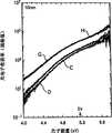
图5是表示氮化硅膜(膜厚3nm)的PYS测定结果的图。Fig. 5 is a graph showing the results of PYS measurement of a silicon nitride film (thickness: 3 nm).
图6是表示氮化硅膜(膜厚10nm)的PYS测定结果的图。Fig. 6 is a graph showing the results of PYS measurement of a silicon nitride film (thickness: 10 nm).
图7是表示氮化硅膜和氢终端Si(100)面的PYS测定结果的图。FIG. 7 is a graph showing the results of PYS measurements of a silicon nitride film and a hydrogen-terminated Si(100) surface.
图8是表示氮化硅膜的电子占有缺陷密度的深度方向分布的图。FIG. 8 is a graph showing the distribution in the depth direction of the electron-occupancy defect density of a silicon nitride film.
图9是表示通过XPS分析测定的氮化硅膜的化学组成分布的图。FIG. 9 is a graph showing the chemical composition distribution of a silicon nitride film measured by XPS analysis.
图10是表示通过LPCVD的试验分区I的氮化硅膜的电子占有缺陷的深度方向分布的图。FIG. 10 is a graph showing the distribution in the depth direction of electron-occupied defects in a silicon nitride film in a test section I by LPCVD.
图11是表示试验分区J的氮化硅膜的电子占有缺陷密度的深度方向分布的图。11 is a graph showing the distribution in the depth direction of the electron-occupied defect density of the silicon nitride film in the test section J. FIG.
图12是表示通过LPCVD的试验分区I的氮化硅膜的XPS分析结果的图。FIG. 12 is a graph showing the results of XPS analysis of the silicon nitride film of the test partition I by LPCVD.
图13是表示试验分区J的氮化硅膜的XPS分析结果的图。FIG. 13 is a graph showing the results of XPS analysis of the silicon nitride film in the test section J. FIG.
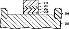
图14是表示本发明的一种实施方式的非易失性半导体存储装置的大致结构的剖面图。14 is a cross-sectional view showing a schematic configuration of a nonvolatile semiconductor memory device according to an embodiment of the present invention.
图15是表示利用本发明第一实施方式的氮化硅膜的形成方法的非易失性半导体存储装置的制造工序的工序剖面图。15 is a process sectional view showing the manufacturing process of the nonvolatile semiconductor memory device using the silicon nitride film forming method according to the first embodiment of the present invention.
图16是表示利用本发明第一实施方式的氮化硅膜的形成方法的非易失性半导体存储装置的制造工序的工序剖面图。16 is a process sectional view showing the manufacturing process of the nonvolatile semiconductor memory device using the silicon nitride film forming method according to the first embodiment of the present invention.
图17是表示利用本发明第一实施方式的氮化硅膜的形成方法的非易失性半导体存储装置的制造工序的工序剖面图。17 is a process sectional view showing the manufacturing process of the nonvolatile semiconductor memory device using the silicon nitride film forming method according to the first embodiment of the present invention.
图18是表示利用本发明第一实施方式的氮化硅膜的形成方法的非易失性半导体存储装置的制造工序的工序剖面图。18 is a process sectional view showing the manufacturing process of the nonvolatile semiconductor memory device using the silicon nitride film forming method according to the first embodiment of the present invention.
图19是表示利用本发明第一实施方式的氮化硅膜的形成方法的非易失性半导体存储装置的制造工序的工序剖面图。19 is a process cross-sectional view showing the manufacturing process of the nonvolatile semiconductor memory device using the silicon nitride film forming method according to the first embodiment of the present invention.
图20是表示利用本发明第一实施方式的氮化硅膜的形成方法的非易失性半导体存储装置的制造工序的工序剖面图。20 is a process sectional view showing the manufacturing process of the nonvolatile semiconductor memory device using the silicon nitride film forming method according to the first embodiment of the present invention.
图21是表示本发明第二实施方式的氮化硅膜的形成方法的大致顺序的流程图。FIG. 21 is a flowchart showing a general procedure of a method for forming a silicon nitride film according to a second embodiment of the present invention.
图22是表示本发明的其他实施方式的非易失性半导体存储装置的大致结构的说明图。22 is an explanatory diagram showing a schematic configuration of a nonvolatile semiconductor memory device according to another embodiment of the present invention.
图23是表示氮化硅膜的XPS分析结果的图。FIG. 23 is a graph showing the results of XPS analysis of a silicon nitride film.
具体实施方式Detailed ways
下面,参照附图说明本发明优选的实施方式。Next, preferred embodiments of the present invention will be described with reference to the drawings.
<第一实施方式><First Embodiment>
图1是示意性地表示适用于本发明的氮化硅膜的形成方法实施的等离子体处理装置的一个示例的大致结构的剖面图,图2是表示图1的等离子体处理装置的平面天线的平面图,图3是表示图1的等离子体处理装置的控制部的结构的框图。1 is a cross-sectional view schematically showing an example of a rough structure of a plasma processing apparatus suitable for implementing the method for forming a silicon nitride film according to the present invention, and FIG. 2 is a diagram showing a planar antenna of the plasma processing apparatus of FIG. 1 In plan view, FIG. 3 is a block diagram showing a configuration of a control unit of the plasma processing apparatus in FIG. 1 .
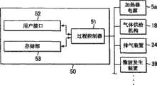
该等离子体处理装置100构成为RLSA微波等离子体处理装置,在该装置中,利用具有多个狭缝状孔的作为平面天线的RLSA(RadialLine Slot Antenna:隙缝天线)向处理室内导入微波,产生等离子体,由此能够产生高密度且低电子温度的微波激发等离子体。在等离子体处理装置100中,能够利用具有1×10¹⁰~5×10¹²/cm3的等离子体密度、并且0.7×2eV的低电子温度的等离子体进行处理。因此,等离子体处理装置100能够适用于在各种半导体装置的制造过程中利用等离子体CVD的氮化硅膜的成膜处理。The
对于等离子体处理装置100,作为主要构成,具备:气密地构成的腔室(处理室)1、向腔室1内供给气体的气体供给机构18、用于对腔室1内进行减压排气的排气装置24、设置在腔室1的上部用于向腔室1内导入微波的微波导入机构27、和用于控制等离子体处理装置100的各构成部的控制部50。The
腔室1为接地的大致为圆筒状的容器,具有例如由铝构成的底壁1a和侧壁1b。其中,腔室1也可以为棱柱形状的容器。The
在腔室1的内部设置有用于水平地支承作为被处理体的硅晶片(以下简称为“晶片”)W的载置台2。载置台2由热传导性高的陶瓷、例如由AlN构成。该载置台2由从排气室11的底部中央向上方延伸的圆筒状的支承部件3支承。支承部件3也由热传导性高的陶瓷、例如AlN构成。Inside the
并且,在载置台2上,罩住其外缘部设置有用于引导晶片W的外罩环4。该外罩环4为例如由石英、AlN、Al2O3、SiN的任一材料构成的环状部件。Furthermore, a
并且,在载置台2中埋入有作为温度调节机构的电阻加热型的加热器5。该加热器5通过来自加热器电源5a的供电对载置台2进行加热,利用该热量对作为被处理基板的晶片W进行均匀加热。In addition, a resistance
此外,在载置台2中设置有热电偶(TC)6。基于由该热电偶6检测出的温度,能够将晶片W控制在例如从室温到900℃的范围内。In addition, a thermocouple (TC) 6 is provided on the mounting table 2 . Based on the temperature detected by the
此外在载置台2上具有用于支承晶片W使其升降的晶片支承销(未图示)。各晶片支承销以相对于载置台2的表面突出没入的方式设置。In addition, the
在腔室1的底壁1a的大致中央部,形成有圆形的开口部10。在底壁1a处设置有与该开口部10连通并向下方突出的排气室11。在该排气室11上连接有排气管12,经由该排气管12与排气装置24连接。A
在形成腔室1的侧壁1b的上端,配置有使腔室1开闭的具有作为盖体(lid:盖)的功能的环状的板13。板13的内周下部向内侧(腔室内空间)突出,形成环状的支承部13a。On the upper end of the
在板13上设置有作为第一气体导入部的呈环状的气体导入部14。并且,在腔室1的侧壁1b,设置有作为第二气体导入部的呈环状的气体导入部15。即,这些气体导入部14和15分上下两段设置。从气体供给机构18向气体导入部14和15供给规定的气体。其中,气体导入部14和15可以为喷嘴状或喷淋头状。并且,气体导入部14和气体导入部15也可以为单一的喷淋头。The
此外,在腔室1的侧壁1b,设置有用于在与等离子体处理装置100邻接的搬送室(未图示)之间进行晶片W的搬入搬出的搬入搬出口16和用于开关该搬入搬出口16的闸阀17。In addition, on the
气体供给机构18例如具有含氮气体(含N气体)供给源19a、含硅气体(含Si气体)供给源19b、惰性气体供给源19c和清洁气体源19d。含氮气体供给源19a与上段气体导入部14连接。并且,含硅气体供给源19b、惰性气体供给源19c和清洁气体供给源19d与下段的气体导入部15连接。其中,作为上述以外的未图示的气体供给源,气体供给机构18具有例如在对腔室内气氛进行置换时使用的吹扫气体供给源等。The gas supply mechanism 18 has, for example, a nitrogen-containing gas (N-containing gas)
作为成膜原料气体的含氮气体,例如可以使用氮气(N2)、氨气(NH3)、MMH(单甲基肼)等肼衍生物等。并且,作为其他成膜原料气体的含硅气体,例如可以使用甲硅烷(SiH4)、乙硅烷(Si2H6)、TSA(三甲硅烷基胺)等。其中,特别优选乙硅烷(Si2H6)。此外,作为惰性气体,例如可以使用N2气体或稀有气体等。稀有气体是用于激发等离子体的气体,例如可以使用Ar气体、Kr气体、Xe气体、He气体等。As the nitrogen-containing gas of the film-forming raw material gas, for example, nitrogen gas (N2 ), ammonia gas (NH3 ), hydrazine derivatives such as MMH (monomethylhydrazine), and the like can be used. Furthermore, as silicon-containing gas of another film-forming raw material gas, for example, monosilane (SiH4 ), disilane (Si2 H6 ), TSA (trisilylamine), or the like can be used. Among them, disilane (Si2 H6 ) is particularly preferable. In addition, as an inert gas,N2 gas, a rare gas, etc. can be used, for example. The rare gas is a gas for exciting plasma, for example, Ar gas, Kr gas, Xe gas, He gas, etc. can be used.
此外,作为清洁气体,可以使用ClF3气体、NF3气体、HCl气体、Cl2气体等,其中NF3气体用于进行等离子体化。In addition, as the cleaning gas, ClF3 gas, NF3 gas, HCl gas, Cl2 gas, etc., among which NF3 gas is used to perform plasmaization, can be used.
含氮气体从气体供给机构18的含氮气体供给源19a经由气体线路20到达气体导入部14,从气体导入部14导入腔室1内。另一方面,含硅气体和惰性性气体从含硅气体供给源19b和惰性性气体供给源19c分别经由气体线路20到达气体导入部15,从气体导入部15导入腔室1内。在与各气体供给源连接的各气体线路20上设置有质量流量控制器21和其前后的开关阀22。利用这种气体控制机构18的构成,能够实现供给的气体的切换和流量等的控制。其中,Ar等的用于等离子体激发的稀有气体可以为任意气体,不一定必须与成膜原料气体同时供给,但如果考虑到等离子体的生成稳定性,优选同时供给。The nitrogen-containing gas reaches the
排气装置24具备涡轮分子泵等高速真空泵。排气装置24经由排气管12与腔室1的排气室11连接。通过使该排气装置24动作,腔室1内的气体向排气室11的空间11a内均匀流动,并且从空间11a经由排气管12向外部排气。由此,能够将腔室1内高速地减压,例如减压至0.133Pa。The
下面,对微波导入机构27的构成进行说明。对于微波导入机构27,作为主要构成,具有透过板28、平面天线31、滞波件33、外罩34、波导管37和微波发生装置39。Next, the configuration of the microwave introduction mechanism 27 will be described. The microwave introduction mechanism 27 has, as main components, a
透过微波的透过板28由在板13的内侧设置为环状的支承面13a支承。在该透过板28和支承面13a之间,通过密封部件29气密地密封。由此,腔室1内保持气密。透过板28由电介质构成,例如由石英或Al2O3、AlN等陶瓷构成。The microwave-transmitting
平面天线31呈圆板状,在透过板28的上方,与载置台2相对设置。其中,平面天线31的形状并不限于圆板状,例如也可以为四边形板状。该平面天线31与板13的上端卡合。The
平面天线31例如由其表面镀金或镀银的铜板、镍板、不锈钢板或铝板构成。平面天线31具有用于放射微波的多个狭缝状的微波放射孔32。微波放射孔32以规定的图案贯通平面天线31形成。The
如图2所示,各个微波放射孔32为细长状的孔,邻接的两个微波放射孔成对。并且,邻接的微波放射孔32例如配置为“T”字状。并且,这样组合配置为规定形状(例如T字状)的微波放射孔32进一步整体配置为同心圆状。As shown in FIG. 2 , each
微波放射孔32的长度和配列间隔根据微波的波长(λg)决定。例如,微波放射孔32的间隔配置为λg/4至λg。在图2中,形成为同心圆状的邻接的微波放射孔32的间隔用Δr表示。其中,微波放射孔32的形状也可以为圆形、圆弧形等其他形状。并且,微波放射孔32的配置方式没有特定限制,除同心圆状外,例如可以配置为螺旋状、放射状等。The length and arrangement interval of the microwave radiation holes 32 are determined according to the wavelength (λg) of the microwave. For example, the intervals of the microwave radiation holes 32 are arranged from λg/4 to λg. In FIG. 2 , the interval between adjacent concentric microwave radiation holes 32 is represented by Δr. Wherein, the shape of the
在平面天线31的上表面配置有具有大于真空的介电常数的滞波件33。由于微波在真空中的波长增长,该滞波件33具有缩短微波的波长、并调整等离子体的功能。On the upper surface of the
并且,平面天线31与透过板28之间、以及滞波件33与平面天线31之间可以各自接触也可以离开,优选接触。Furthermore, the
在腔室1的上部,以覆盖这些平面天线31和滞波件33的方式设置有具有波导管功能的导电性的外罩34,该外罩34例如由铝或不锈钢、铜等金属材料构成。板13的上端和外罩34由密封部件35密封。在外罩34的内部形成有冷却水流路34a。通过在该冷却水流路34a中流通有冷却水,能够对外罩34、滞波件33、平面天线31和透过板28进行冷却。其中,外罩34接地。On the upper part of the
在外罩34的上壁(天井部)的中央形成有开口部36,在该开口部36上连接有波导管37。波导管37的另一端侧经由匹配回路38连接有产生微波的微波发生装置39。An
波导管37具有:从上述外罩34的开口部36向上方延伸伸出的截面为圆形的同轴波导管37a、和利用模式转换器连接在该同轴波导管37a的上端部的在水平方向延伸的矩形波导管37b。The
内导体41在同轴波导管37a的中心延伸。该内导体41在其下端部连接固定在平面天线31的中心。通过这种结构,微波能够经由同轴波导管37a的内导体41以放射状有效且均匀地向导电性外罩34和平面天线31形成的扁平波导路传播。The
通过上述结构的微波导入机构27,在微波发生装置39中产生的微波经由波导管37向平面天线31传播,并且经由透过板28导入腔室1内。其中,作为微波的频率,例如优选使用2.45GHz,此外,也可以使用8.35GHz、1.98GHz等。With the microwave introduction mechanism 27 configured as described above, microwaves generated in the
等离子体处理装置100的各构成部为与控制部50连接并受其控制的构成。如图3所示,控制部50包括:具备CPU的过程控制器51、与该过程控制器514连接的用户接口52和存储部53。过程控制器51为控制单元,一并控制等离子体处理装置100中的与压力、温度、气体流量等工艺条件相关的各构成部(例如,加热器电源5a、气体供给机构18、排气装置24、微波发生装置39等)。Each component of the
用户接口52具有工序管理者用于管理等离子体处理装置100而进行指令输入操作等的键盘、可视化显示等离子体处理装置100的运转状况的显示器等。存储部53中存储有用于利用过程控制器51的控制实现在等离子体处理装置100中实行的各种处理的控制程序(软件)或记录有处理条件等的方案。The
并且,根据需要,利用来自用户接口52的指示等从存储部53调出任意的方案,由过程控制器51执行,由此在过程控制器51的控制下,实行等离子体处理装置100中的所希望的处理。并且,上述控制程序或处理条件数据等方案可以以存储在计算机能够读取的存储介质例如CD-ROM、硬盘、软盘、闪存等中的状态而利用,或者也可以从其他装置例如通过专用回路随时传送在线利用。And, if necessary, an arbitrary recipe is called from the
在这样构成的等离子体处理装置100中,能够进行在800℃以下的低温下对基底膜等进行无损伤的等离子体CVD处理。并且,等离子体处理装置100的等离子体的均匀性优异,所以能够实现工艺的均匀性。In the
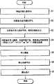
在这样构成的RLSA方式的等离子体处理装置100中,例如按照图4的流程图所示的顺序,利用等离子体CVD法,进行在晶片W表面堆积氮化硅膜的处理。In the RLSA
首先,打开闸阀17,从搬入搬出口16向腔室1内搬入晶片W,将其载置在载置台2上(步骤S1)。接着,对腔室1内进行减压排气(步骤S2)。并且,在进行减压排气的同时,从气体供给机构18的含氮气体供给源19a和含硅气体供给源19b以规定的流量分别经由导入部14、15向腔室1内导入含氮气体和含硅气体(步骤S3)。这样一来,将腔室1内调节为规定的压力。First, the
接着,经由匹配回路38向波导管37内导入在微波发生装置39中产生的规定频率例如2.45GHz的微波(步骤S4)。导入波导管37内的微波依次通过矩形波导管37b和同轴波导管37a,经由内导体41向平面天线31供给。即,微波在同轴波导管37a内向平面天线31传播。并且,微波从平面天线31的狭缝状的微波放射孔32经由透过板28向腔室1内的晶片W的上方空间放射。此时的微波输出优选为,作为平面天线31的每1cm2的面积的功率密度,在0.41~4.19W/cm2的范围内。微波的输出可以根据目的例如从500~5000W的范围内选择,以达到上述范围内的功率密度。Next, microwaves of a predetermined frequency, for example, 2.45 GHz generated by the
利用从平面天线31经过透过板28放射至腔室1内的微波,在腔室1内形成电磁场,含氮气体、含硅气体分别等离子体化。该微波激发的等离子体,通过微波从平面天线31的多个微波辐射孔32放射,以大致1×10¹⁰~5×10¹²/cm3的高密度,并且在晶片W附近,形成大致1.5eV以下的低电子密度。这样形成的微波激发高密度等离子体对基底膜的等离子体损伤很少。并且,原料气体在等离子体中发生解离,通过SipHq、SiHq、NHq、N(这里p、q表示任意的数,下同)等活性种的反应,堆积具有规定大小的陷阱密度的氮化硅膜SixN或氮化氧化硅SixOzNy(这里,x、y、z不一定根据化学量论决定,可以根据条件而取不同的值,为任意的数)的薄膜。The microwaves radiated from the
在本发明中,通过选择使用等离子体处理装置100的等离子体CVD成膜的条件,将形成的氮化硅膜的陷阱密度控制为所希望的大小。In the present invention, the trap density of the formed silicon nitride film is controlled to a desired value by selecting the conditions of the plasma CVD film formation using the
例如在减小形成的氮化硅膜中的陷阱密度的情况下(例如陷阱密度以面密度计在5×10¹⁰~5×1012cm-2eV-1的范围内),选择第一条件。在该第一条件下,优选使用氮气N2作为含氮气体,使用Si2H6气体作为含硅气体。此时,从以均匀的膜厚形成Si密度低的氮化硅膜的观点出发,优选N2气体与Si2H6气体的流量比(N2气体流量/Si2H6气体流量)在0.1~5000的范围内,更优选在100~2000的范围内。具体而言,使N2气体的流量在10~5000mL/min(sccm)的范围内,优选在100~2000mL/min(sccm)的范围内;使Si2H6气体的流量在0.5~100mL/min(sccm)的范围内,优选在0.5~10mL/min(sccm)的范围内,设定为上述流量比。此外,在使用上述N2气体和Si2H6气体的第一条件下,为了形成具有小的陷阱密度的氮化硅膜,优选使处理压力为0.1~500Pa,更优选为1~100Pa。并且,优选使微波的功率密度在0.41~4.19W/cm2(平面天线31的每1cm2的面积)的范围内。For example, in the case of reducing the trap density in the formed silicon nitride film (for example, the trap density is in the range of 5×10¹⁰ to 5×1012 cm−2 eV−1 in terms of areal density), the first condition is selected . Under this first condition, nitrogen gas N2 is preferably used as the nitrogen-containing gas, and Si2 H6 gas is used as the silicon-containing gas. At this time, from the viewpoint of forming a silicon nitride film with a uniform film thickness and a low Si density, the flow ratio of N2 gas to Si2 H6 gas (N2 gas flow rate/Si2 H6 gas flow rate) is preferably 0.1 It is in the range of ∼5000, more preferably in the range of 100-2000. Specifically, the flow rate of N2 gas is in the range of 10 to 5000 mL/min (sccm), preferably in the range of 100 to 2000 mL/min (sccm); the flow rate of Si2 H6 gas is in the range of 0.5 to 100 mL/min The above flow rate ratio is set within the range of min (sccm), preferably within the range of 0.5 to 10 mL/min (sccm). In addition, under the first condition using the above-mentioned N2 gas and Si2 H6 gas, in order to form a silicon nitride film having a small trap density, the processing pressure is preferably 0.1 to 500 Pa, more preferably 1 to 100 Pa. In addition, it is preferable to set the power density of the microwave in the range of 0.41 to 4.19 W/cm2 (per 1 cm2 of the area of the planar antenna 31 ).
此外,例如在增大形成的氮化硅膜中的陷阱密度的情况下(例如陷阱密度以面密度计在1×10¹¹~1×1013cm-2eV-1的范围内),选择第二条件。在该第二条件下,优选使用NH3气体作为含氮气体,使用Si2H6气体作为含硅气体。此时,从以均匀的膜厚形成Si密度高的氮化硅膜的观点出发,优选NH3气体与Si2H6气体的流量比(NH3气体流量/Si2H6气体流量)在0.1~1000的范围内,更优选在100~300的范围内。具体而言,使NH3气体的流量在10~5000mL/min(sccm)的范围内,优选在100~2000mL/min(sccm)的范围内;使Si2H6气体的流量在0.5~100mL/min(sccm)的范围内,优选在1~50mL/min(sccm)的范围内,设定为上述流量比。此外,在使用上述NH3气体和Si2H6气体的第二条件下,为了形成具有大的陷阱密度的氮化硅膜,优选使处理压力为1~1333Pa,更优选为50~650Pa。并且,优选使微波的功率密度在0.41~4.19W/cm2(平面天线31的每1cm2的面积)的范围内。In addition, for example, in the case of increasing the trap density in the formed silicon nitride film (for example, the trap density is in the range of 1×10¹¹ to 1×1013 cm−2 eV−1 in terms of areal density), the second Two conditions. Under this second condition, it is preferable to use NH3 gas as the nitrogen-containing gas and Si2 H6 gas as the silicon-containing gas. At this time, from the viewpoint of forming a silicon nitride film having a high Si density with a uniform film thickness, it is preferable that the flow rate ratio of NH3 gas to Si2 H6 gas (NH3 gas flow rate/Si2 H6 gas flow rate) is 0.1. to 1000, more preferably 100 to 300. Specifically, the flow rate of NH3 gas is in the range of 10 to 5000 mL/min (sccm), preferably in the range of 100 to 2000 mL/min (sccm); the flow rate of Si2 H6 gas is in the range of 0.5 to 100 mL/min. The above-mentioned flow ratio is set within the range of min (sccm), preferably within the range of 1 to 50 mL/min (sccm). In addition, under the second condition using the above-mentioned NH3 gas and Si2 H6 gas, in order to form a silicon nitride film having a large trap density, the processing pressure is preferably 1 to 1333 Pa, more preferably 50 to 650 Pa. In addition, it is preferable to set the power density of the microwave in the range of 0.41 to 4.19 W/cm2 (per 1 cm2 of the area of the planar antenna 31 ).
此外,通过等离子体处理装置100以上述第二条件进行CVD,能够形成在膜的厚度方向具有大致均等的陷阱密度分布的氮化硅膜。即,例如能够形成相当于硅的禁带中央的能量位置的陷阱的体积密度在膜的厚度方向在1×10¹⁷~5×1017cm-3eV-1的范围内分布、从与基底硅层的界面向表面侧上述陷阱的体积密度在1×10¹⁷~2×1017cm-3eV-1的范围内分布的氮化硅膜。此时,优选形成的氮化硅膜的膜厚在1~20nm的范围内,更优选在3~15nm的范围内。其中,通过取上述陷阱的体积密度的2/3次方,能够换算成面密度。Furthermore, by performing CVD in the
此外,在上述第一条件和第二条件的任一种情况下,对于等离子体CVD的处理温度,优选使载置台2的温度在300℃以上800℃以下,更优选加热至400~600℃。此外,从以均匀的膜厚和膜质形成氮化硅膜的观点出发,优选将等离子体处理装置100中的间隙(从透过板28的下表面到载置台2的上表面的间隔)G设定为例如50~500mm左右。In addition, under either of the above-mentioned first condition and second condition, the temperature of the
然后,停止供给微波,结束氮化硅膜的形成(步骤S5)。接着,停止从气体供给机构18供给气体(步骤S6)。然后,在氮化硅膜的堆积结束后,通过将形成有氮化硅膜的晶片W从腔室1内搬出,对1片晶片W的处理结束(步骤S7)。Then, the supply of microwaves is stopped, and the formation of the silicon nitride film is completed (step S5). Next, gas supply from the gas supply mechanism 18 is stopped (step S6). Then, after the deposition of the silicon nitride film is completed, the wafer W on which the silicon nitride film is formed is carried out from the
在利用使用等离子体处理装置100的等离子体CVD形成氮化硅膜时,通过在二氧化硅膜(SiO2)膜上堆积氮化硅膜,能够进一步增大氮化硅膜的陷阱密度。因此,在本发明中,在基底层例如为由单晶硅构成的硅基板或多晶硅层的情况下,优选预先在基底层的表面形成SiO2的薄膜。在这种情况下,SiO2的薄膜可以是自然氧化膜,可以是热氧化膜,也可以是等离子体氧化膜。并且,也可以利用例如HPM(盐酸双氧水)、SPM(硫酸双氧水)这种具有氧化作用的药剂,对Si表面进行化学处理,预先形成化学氧化膜(Chemical Oxide)。作为预先在基底层的表面形成的SiO2薄膜的膜厚,例如优选为0.1~10nm,更优选为0.1~3nm。When the silicon nitride film is formed by plasma CVD using the
利用本实施方式的氮化硅膜的形成方法形成的氮化硅膜的陷阱密度,可以利用例如光电子收获率分光法(Photoemission YieldSpectroscopy:PYS)进行测定。PYS是对试样(氮化硅膜)照射一定能量的光,将通过光电效应放出的光电子的全部放出光电子量作为入射光的能量的函数进行测定的方法。通过该PYS测定,能够以非破坏的方式以高灵敏度测定氮化硅膜中以及氮化硅膜与硅层的界面的缺陷能级密度分布。由PYS测定的光电子收获率相当于电子占有状态密度分布的能量积分,所以能够利用S.Miyazaki等的方法(Microelectron.Eng.48(1999)63.)由微分PYS谱求出欠缺能级密度分布。The trap density of the silicon nitride film formed by the silicon nitride film forming method of this embodiment can be measured by, for example, photoemission yield spectroscopy (PYS). PYS is a method of irradiating a sample (silicon nitride film) with light of a certain energy, and measuring the total emitted photoelectron amount of photoelectrons emitted by the photoelectric effect as a function of the energy of incident light. By this PYS measurement, the defect level density distribution in the silicon nitride film and at the interface between the silicon nitride film and the silicon layer can be measured non-destructively and with high sensitivity. The photoelectron harvest rate measured by PYS is equivalent to the energy integral of the density distribution of electron occupation states, so the method of S. Miyazaki et al. (Microelectron. Eng. 48 (1999) 63.) can be used to obtain the lack level density distribution from the differential PYS spectrum .
下面,对于确认本发明效果的试验结果进行说明。使用等离子体处理装置100,改变条件在p型硅基板(10Ω·cm)上形成氮化硅膜。利用PYS对得到的氮化硅膜进行测定。关于PYS测定,使用紫外线灯,向各氮化硅膜照射紫外线,通过利用光电子增倍管测定放出的电子而进行。在本试验中,对于以下表1所示的试验分区A~H进行实验。Next, the test results for confirming the effects of the present invention will be described. Using the
[表1][Table 1]
表1所示的等离子体CVD条件的内容如下所示。The contents of the plasma CVD conditions shown in Table 1 are as follows.
<等离子体CVD条件1:N2/Si2H6气体系><Plasma CVD Condition 1: N2 /Si2 H6 Gas System>
N2气体流量:1200mL/min(sccm)N2 gas flow rate: 1200mL/min(sccm)
Si2H6气体流量:3mL/min(sccm)Si2 H6 gas flow rate: 3mL/min(sccm)
流量比(N2/Si2H6):400Flow ratio (N2 /Si2 H6 ): 400
处理压力:7.6PaHandling pressure: 7.6Pa
载置台2的温度:500℃Temperature of stage 2: 500°C
微波功率:2000WMicrowave power: 2000W
微波功率密度:1.67W/cm2(平面天线31的每1cm2的面积)Microwave power density: 1.67W/cm2 (per 1 cm2 area of the planar antenna 31)
<等离子体CVD条件2:NH3/Si2H6气体系><Plasma CVD Condition 2: NH3 /Si2 H6 Gas System>
NH3气体流量:800mL/min(sccm)NH3 gas flow rate: 800mL/min(sccm)
Si2H6气体流量:10mL/min(sccm)Si2 H6 gas flow rate: 10mL/min(sccm)
流量比(NH3/Si2H6):80Flow ratio (NH3 /Si2 H6 ): 80
处理压力:126PaHandling pressure: 126Pa
载置台2的温度:500℃Temperature of stage 2: 500°C
微波功率:2000WMicrowave power: 2000W
微波功率密度:1.67W/cm2(平面天线31的每1cm2的面积)Microwave power density: 1.67W/cm2 (per 1 cm2 area of the planar antenna 31)
表1所示的前处理的内容如下所述。The contents of the preprocessing shown in Table 1 are as follows.
<DHF处理><DHF processing>
在等离子体CVD之前,用1%的稀氢氟酸溶液对硅基板的表面进行处理,除去自然氧化膜。Before plasma CVD, the surface of the silicon substrate is treated with 1% dilute hydrofluoric acid solution to remove the natural oxide film.
<HPM处理><HPM processing>
在等离子体CVD之前,用1%的稀氢氟酸溶液对硅基板的表面进行处理,除去自然氧化膜。然后用10%HPM(盐酸双氧水)进行处理,形成作为化学氧化膜(Chemical Oxide膜)的SiO2膜。Before plasma CVD, the surface of the silicon substrate is treated with 1% dilute hydrofluoric acid solution to remove the natural oxide film. Then, it was treated with 10% HPM (hydrogen peroxide) to form a SiO2 film as a chemical oxide film (Chemical Oxide film).
图5和图6表示PYS测定的结果。图5中氮化硅膜的膜厚为3nm的结果,图6中氮化硅膜的膜厚为10nm的结果。与使用氮气作为原料气体在等离子体CVD条件1下形成的氮化硅膜(试验分区A、B、C、D)相比,使用氨气作为原料气体在等离子体CVD条件2下形成的氮化硅膜(试验分区E、F、G、H)的光电子收获率大,显示陷阱密度高。Figures 5 and 6 show the results of the PYS assay. The result of the film thickness of the silicon nitride film in FIG. 5 being 3 nm, and the result of the film thickness of the silicon nitride film in FIG. 6 of 10 nm. Compared with the silicon nitride film formed under
此外,对于由于等离子体CVD条件的差异而导致的缺陷能级密度的差,氮化硅膜的膜厚为3nm的情况(试验分区A、B、E、F)比为10nm(试验分区C、D、G、H)的情况表现得更显著。并且,如图5所示,对氮化硅膜的膜厚为3nm的试验分区E和F进行比较,即使等离子体CVD条件相同,通过进行HPM处理作为前处理,预先在硅基板的表面形成化学氧化物SiO2层,能够得到具有大的缺陷能级密度的氮化硅膜。In addition, regarding the difference in defect level density due to the difference in plasma CVD conditions, the case where the film thickness of the silicon nitride film is 3 nm (test divisions A, B, E, F) is 10 nm (test divisions C, The case of D, G, H) is more pronounced. In addition, as shown in FIG. 5 , comparing test sections E and F with a silicon nitride film thickness of 3 nm, even if the plasma CVD conditions are the same, by performing HPM treatment as a pretreatment, a chemical layer is formed in advance on the surface of the silicon substrate. Oxide SiO2 layer, a silicon nitride film with a large defect level density can be obtained.
接着,对于使用等离子体处理装置100通过等离子体CVD形成的氮化硅膜,定量研究化学组成分布和缺陷能级密度分布,研究两者的关系。在p型硅基板(10Ω·cm)的Si(100)面上,进行HPM处理形成化学氧化物SiO2层,然后以温度400℃形成厚度为11.4nm的氮化硅膜。等离子体CVD的条件如下所示。Next, the chemical composition distribution and defect level density distribution of the silicon nitride film formed by plasma CVD using the
<等离子体CVD条件3:NH3/Si2H6气体系><Plasma CVD Condition 3: NH3 /Si2 H6 Gas System>
NH3气体流量:800mL/min(sccm)NH3 gas flow rate: 800mL/min(sccm)
Si2H6气体流量:16mL/min(sccm)Si2 H6 gas flow rate: 16mL/min(sccm)
流量比(NH3/Si2H6):50Flow ratio (NH3 /Si2 H6 ): 50
处理压力:126PaHandling pressure: 126Pa
载置台2的温度:400℃Temperature of stage 2: 400°C
微波功率:2000WMicrowave power: 2000W
微波功率密度:1.67W/cm2(平面天线31的每1cm2的面积)Microwave power density: 1.67W/cm2 (per 1 cm2 area of the planar antenna 31)
用稀氢氟酸对形成的氮化硅膜进行蚀刻处理,使其薄膜化,在各蚀刻过程中进行PYS测定和X射线光电子分光(XPS)测定。图7表示对制作的氮化硅膜[SiNx/Si(100)]和进行60秒蚀刻后的氢终端Si(100)[H-p+Si(100)]进行PYS测定。根据该图7显示,在氮化硅膜[SiNx/Si(100)]中,在相当于Si带隙的能量区域存在着电子占有缺陷(陷阱),所以在低于Si价电子带上端(Ev)的能量区域(<5.15eV),来自氮化硅膜的光电子收获率显著高于氢终端Si(100)。The formed silicon nitride film was etched with dilute hydrofluoric acid to make it thinner, and PYS measurement and X-ray photoelectron spectroscopy (XPS) measurement were performed during each etching process. FIG. 7 shows the PYS measurement of the fabricated silicon nitride film [SiNx /Si(100)] and the hydrogen-terminated Si(100) [H-p+Si(100)] etched for 60 seconds. According to this figure 7, in the silicon nitride film [SiNx /Si(100)], there are electron occupation defects (trap) in the energy region corresponding to the Si band gap, so the electron occupation defect (trap) exists below the upper end of the Si valence band ( In the energy region of Ev) (<5.15eV), the photoelectron harvest rate from the silicon nitride film is significantly higher than that of the hydrogen-terminated Si(100).
此外,图8表示由各蚀刻过程中的光电子收获率的变化量估算电子占有缺陷的深度方向的分布的结果。如该图8所示,可以确认在比Si价电子带上端(Ev)浅0.28eV的能量位置(E-Ev=0.28eV)的电子占有缺陷密度,在Si基板界面附近最大(~6.0×1018cm-3eV-1),在距Si基板界面4nm左右的区域最小(~3.2×1017cm-3eV-1)。并且,在相当于硅的禁带中央的能量位置(E-Ev=0.56eV),Si界面附近的电子占有缺陷密度分布显著降低,而在氮化硅膜中,得到与价电子带侧相同的电子占有缺陷密度分布。In addition, FIG. 8 shows the results of estimating the distribution of electron-occupied defects in the depth direction from the amount of change in photoelectron yield in each etching process. As shown in FIG. 8, it can be confirmed that the electron-occupied defect density at the energy position (E-Ev=0.28eV) shallower than the upper end (Ev) of the Si valence band by 0.28eV is the largest near the Si substrate interface (~6.0×1018 cm-3 eV-1 ), and the smallest (~3.2×1017 cm-3 eV-1 ) at about 4 nm from the Si substrate interface. In addition, at the energy position corresponding to the center of the forbidden band of silicon (E-Ev=0.56eV), the distribution of the electron-occupancy defect density near the Si interface is significantly reduced, and in the silicon nitride film, the same Electron occupation defect density distribution.
图9表示通过XPS分析测定的氮化硅膜的化学组成分布图。在图9中,可知氮化硅膜的表面附近的区域和距离Si基板界面厚度约3nm以内的区域,氧原子显著地向氮化硅膜中扩散、混入。可以认为表面侧的氧化缘于自然氧化,Si基板界面侧则缘于化学氧化物SiO2层与氮化硅膜的界面反应。Fig. 9 is a graph showing the chemical composition distribution of the silicon nitride film measured by XPS analysis. In FIG. 9 , it can be seen that oxygen atoms are significantly diffused and mixed into the silicon nitride film in the region near the surface of the silicon nitride film and in the region within about 3 nm in thickness from the Si substrate interface. It can be considered that the oxidation on the surface side is due to natural oxidation, and the oxidation on the Si substrate interface side is due to the interface reaction between the chemical oxideSiO2 layer and the silicon nitride film.
将图8中的相当于硅的禁带中央的能量位置(E-Ev=0.56eV)的结果与图9所示的通过XPS测定的氮化硅膜的化学组成分布图进行比较,在距离Si基板界面约2nm附近,电子占有缺陷局部增大的区域相当于化学氧化物SiO2层与氮化硅膜的界面附近。由此可知,使用等离子体处理装置100,在通过等离子体CVD条件3成膜的氮化硅膜中,在氧原子扩散、混入的化学氧化物SiO2层与氮化硅膜的界面附近,膜中的电子占有缺陷密度显著增大。Comparing the results of the energy position (E-Ev=0.56eV) corresponding to the center of the forbidden band of silicon in FIG. 8 with the chemical composition distribution map of the silicon nitride film measured by XPS shown in FIG. Around 2nm from the substrate interface, the region where the electron occupation defect locally increases corresponds to the vicinity of the interface between the chemical oxide SiO2 layer and the silicon nitride film. From this, it can be seen that in the silicon nitride film formed under the
下面,对于在不同的条件下形成的两种氮化硅膜(试验分区I和J),在图10和图11中表示相当于硅的禁带中央的能量位置的电子占有缺陷在深度方向的分布的测定结果。此外,在图12和图13中表示通过XPS分析测定试验分区I和J的氮化硅膜的化学组成分布图的结果。试验分区I(比较例)是通过下述条件的LPCVD(Low Pressure ChemicalVapor Deposition)形成的膜厚为13nm的氮化硅膜;分区J是使用等离子体处理装置100以上述等离子体CVD条件2形成的膜厚为4.1nm的氮化硅膜。在试验分区I和试验分区J中,均在Si(100)面上通过上述条件的HPM处理形成膜厚为3nm的化学氧化物SiO2层,并在其上进行CVD。Next, for two kinds of silicon nitride films (experimental partitions I and J) formed under different conditions, Fig. 10 and Fig. 11 show the electron-occupied defects at the energy position corresponding to the center of the forbidden band of silicon in the depth direction. The result of the distribution measurement. In addition, FIG. 12 and FIG. 13 show the results of measuring the chemical composition profiles of the silicon nitride films in the test sections I and J by XPS analysis. Experimental partition I (comparative example) is a silicon nitride film with a film thickness of 13 nm formed by LPCVD (Low Pressure Chemical Vapor Deposition) under the following conditions; partition J is formed using the
<LPCVD条件><LPCVD conditions>
SiH2Cl2气体流量:10mL/min(sccm)SiH2 Cl2 gas flow rate: 10mL/min(sccm)
NH3气体流量:1000mL/min(sccm)NH3 gas flow rate: 1000mL/min(sccm)
流量比(NH3/SiH2Cl2):100Flow ratio (NH3 /SiH2 Cl2 ): 100
处理压力:133PaHandling pressure: 133Pa
载置台2的温度:800℃Temperature of stage 2: 800°C
在图10中对于通过LPCVD成膜的试验分区I(比较例)的氮化硅膜,表示相当于硅的禁带中央的能量位置(E-Ev=0.56eV)和比Si价电子带上端(Ev)浅0.84eV的能量位置(E-Ev=0.84eV)的电子占有缺陷的体积密度。由该图10可知,对于通过LPCVD成膜的试验分区I的氮化硅膜,在距离Si(100)界面约10nm的膜厚的范围,在相当于硅的禁带中央的能量位置(E-Ev=0.56eV)的电子占有缺陷密度大致为1×1017cm-3eV-1以下。即,对于试验分区I的氮化硅膜,电子占有缺陷密度整体降低,可能导致容易发生电荷的脱离。10 shows the energy position (E-Ev=0.56eV) corresponding to the center of the forbidden band of silicon and the upper end of the Si valence band ( Ev) Bulk density of electron-occupied defects at an energy position as shallow as 0.84 eV (E-Ev=0.84 eV). As can be seen from FIG. 10 , for the silicon nitride film in the experimental zone I formed by LPCVD, the energy position corresponding to the center of the forbidden band of silicon (E- The electron occupation defect density at Ev=0.56 eV) is approximately 1×1017 cm−3 eV−1 or less. That is, in the silicon nitride film of the test section I, the density of electron-occupancy defects decreased as a whole, and charge detachment may easily occur.
另一方面,在使用氨气和乙硅烷作为原料气体在等离子体CVD条件2下成膜的作为本发明范围的试验分区J中,由图11可以确认,电子占有缺陷在膜厚方向大致均匀分布,其绝对值也大于试验分区I。即,对于试验分区J的氮化硅膜,在相当于硅的禁带中央的能量位置的电子占有缺陷密度在其厚度方向在1×10¹⁷~5×1017cm-3eV-1的范围内大致均等地分布。这样,对于膜的厚度方向上均等且具有大的绝对值的陷阱密度的试验分区J的氮化硅膜,注入的电荷保持在膜的中央部分,所以不容易发生电荷的脱离,电荷蓄积能力高。因此,通过使用这种控制电子占有缺陷在膜厚方向均匀的氮化硅膜作为SONOS(MONOS)结构的半导体存储装置的电荷蓄积层,能够期待优异的电荷蓄积能力。On the other hand, in the experimental zone J, which is the scope of the present invention, in which a film is formed under
并且,如图11所示,试验分区J的氮化硅膜具有4nm的厚度,除去界面附近区域和容易被氧化的表面区域,在从Si基板界面向表面侧厚度1nm~3nm的范围,相当于硅的禁带中央的能量位置的电子占有缺陷密度分布在1×10¹⁷~5×1017cm-3eV-1的窄的范围。即,能够在氮化硅膜中形成具有非常均匀的陷阱密度分布的部分,即使在这种膜厚薄的情况下,也能够发挥足够高的电荷蓄积能力。因此,通过使用这种电子占有缺陷在厚度方向上均匀的氮化硅膜,能够充分对应于半导体存储装置的可靠性和微细化。其中,这种在厚度方向陷阱密度均匀分布的氮化硅膜在厚度1~20nm的范围内能够发挥良好的电荷蓄积能力。And, as shown in FIG. 11 , the silicon nitride film in the test section J has a thickness of 4 nm, and the thickness of the silicon nitride film from the Si substrate interface to the surface side is in the range of 1 nm to 3 nm, which is equivalent to The electron occupation defect density distribution at the energy position in the center of the forbidden band of silicon falls within a narrow range of 1×10¹⁷ to 5×1017 cm−3 eV−1 . That is, a portion having a very uniform trap density distribution can be formed in the silicon nitride film, and even when the film thickness is thin, a sufficiently high charge storage capability can be exhibited. Therefore, by using a silicon nitride film in which such electron occupation defects are uniform in the thickness direction, it is possible to sufficiently cope with reliability and miniaturization of a semiconductor memory device. Among them, such a silicon nitride film having a uniform distribution of trap density in the thickness direction can exhibit good charge storage capability within a thickness range of 1 to 20 nm.
另外,由图12所示的化学组成分布图可知,在试验分区I(比较例)的氮化硅膜中,膜中的氧浓度在Si(100)界面附近和表面附近高,而在膜中央附近几乎不存在氧。另一方面,由图13所示的化学组成分布图可知,在试验分区J的氮化硅膜中,在膜中央附近存在接近20原子%的氧。In addition, from the chemical composition distribution diagram shown in FIG. 12, it can be seen that in the silicon nitride film of the test zone I (comparative example), the oxygen concentration in the film is high near the Si(100) interface and near the surface, and is high in the center of the film. There is almost no oxygen nearby. On the other hand, as can be seen from the chemical composition profile shown in FIG. 13 , in the silicon nitride film of the test section J, approximately 20 atomic % of oxygen exists near the center of the film.
根据图10~图13的比较可以判断,着眼于氮化硅膜中的氧在膜厚方向的分布,在存在氧的区域电子占有缺陷密度增大,另一方面,即使氧超过20原子%,电子占有缺陷密度也不会与氧的增加成比例地增加,为最大值。因此,推测在氮化硅膜中在进行利用2价的氧原子置换3价的氮原子的反应的过程中生成的悬挂键与氮化硅膜中存在的电子占有缺陷相关。From the comparison of Fig. 10 to Fig. 13, it can be judged that focusing on the distribution of oxygen in the film thickness direction in the silicon nitride film, the density of electron occupation defects increases in the region where oxygen exists. On the other hand, even if oxygen exceeds 20 atomic %, The electron-occupancy defect density does not increase in proportion to the increase in oxygen, and reaches a maximum value. Therefore, it is presumed that the dangling bonds generated during the reaction of substituting trivalent nitrogen atoms with divalent oxygen atoms in the silicon nitride film are related to electron occupation defects present in the silicon nitride film.
如上所述,使用等离子体处理装置100,选择等离子体CVD条件而形成的氮化硅膜是电子占有缺陷密度得到高精度控制的膜,在膜的厚度方向具有均等的陷阱密度。As described above, the silicon nitride film formed by selecting the plasma CVD conditions using the
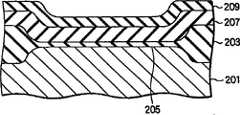
下面,对于将本实施方式的氮化硅膜的形成方法应用于制造半导体装置的例子进行说明。在此,作为半导体装置,以n沟道型非易失性半导体存储装置为例进行说明。图14是表示本发明的一个实施方式所谓非易失性半导体存储装置200的截面结构的说明图。图15至图20是用于说明本实施方式的非易失性半导体存储装置的制造工序的工序剖面图。Next, an example in which the method for forming a silicon nitride film according to this embodiment is applied to the manufacture of a semiconductor device will be described. Here, as a semiconductor device, an n-channel nonvolatile semiconductor memory device will be described as an example. FIG. 14 is an explanatory diagram showing a cross-sectional structure of a so-called nonvolatile
如图14所示,非易失性半导体存储装置200例如具有在p型硅基板(Si基板)201上从下开始依次形成有隧道氧化膜205、氮化硅膜207、氧化硅膜209和电极211的元件结构S。As shown in FIG. 14, the nonvolatile
隧道氧化膜205例如由具有0.1~10nm左右膜厚的SiO2膜或SiNO膜构成。氮化硅膜207作为电荷蓄积层发挥作用,所以例如由1~50nm左右膜厚的SiN膜或SiNO膜构成。并且,也可以设置2层以上的氮化硅膜作为电荷蓄积层。氧化硅膜209是例如通过CVD法形成的SiO2膜,在电极211与氮化硅膜207之间作为阻隔(阻挡)层发挥作用。该氧化硅膜209例如具有0.1~50nm左右膜厚。电极211例如由通过CVD法形成的多晶硅膜构成,作为控制栅极(CG)电极发挥作用。并且。电极211也可以为例如含有钨、钛、钽、铜、铝、金这样的金属的膜。电极211例如具有0.1~50nm左右膜厚。电极211不限于单层机构,以降低电极211的比电阻、实现高速化为目的,可以形成为例如含有钨、钼、钽、钛以及它们的硅化物、氮化物、合金等的叠层结构。该电极211与未图示的配线层连接。The
并且,非易失性半导体存储装置200可以在半导体基板内的p晶片或p型硅层上形成。Also, the nonvolatile
此外,在Si基板201的表面,形成有元件分离膜203,通过该元件分离膜203,划分形成非易失性半导体存储装置200的有源区域A。在Si基板201的原件结构S周围的区域,形成有源极区域212和漏极区域214。在有源区域A内,夹在源极区域212和漏极区域214之间的部分成为非易失性半导体存储装置200的沟道形成区域216。并且,在元件结构S的两侧部形成有侧壁218。In addition, an
对于上述结构的非易失性半导体存储装置200的动作例进行说明。首先,在数据写入时,以Si基板201的电位为基准,将源极区域212和漏极区域214保持在0V,向电极211施加规定的正电压。此时,在沟道形成区域216蓄积电子,形成反转层,由于隧道效应,该反转层内的电子的一部分通过隧道氧化膜205移动至氮化硅膜207。移动至氮化硅膜207的电子被形成于氮化硅膜207内的作为电荷陷阱中心的陷阱所捕获,进行数据的蓄积。An example of the operation of the nonvolatile
在数据读出时,以Si基板201的电位为基准,使源极区域212或漏极区域214的任意一个为0V,向另一个施加规定的电压。并且,也向电极211施加规定的电压。通过这样施加电压,对应于蓄积在氮化硅膜207内的电子的有无、蓄积的电子的量,沟道的电流量和漏极电压发生变化。因此,能够通过检测出该沟道电流或漏极电压的变化,向外部读出存储数据。At the time of data reading, either one of the
在数据消去时,以Si基板201的电位为基准,使源极区域212和漏极区域214两者均为0V,向电极211施加规定大小的负电压。通过施加这样的电压,保持在氮化硅膜207内的电子通过隧道氧化膜205取出至沟道形成区域216。由此,非易失性存储装置200恢复到氮化硅膜207内的电子蓄积量低的消去状态。When erasing data, the
在制造这种非易失性半导体存储装置200时,首先,如图15所示,采用例如LOCOS(Local Oxidation of Silicon)法或STI(Shallow TenchIsolation)法等方法在Si基板201上形成元件分离膜203。并且,为了调整非易失性半导体存储装置200的阈值电压,采用离子注入等方法进行杂质的掺杂。When manufacturing this nonvolatile
接着,例如通过热氧化法在Si基板201的有源区域A的表面形成氧化硅膜。由此,如图16所示形成隧道氧化膜205。并且,可以根据需要对氧化硅膜表面进行氮化处理得到氧氮化硅膜(SiON膜)。Next, a silicon oxide film is formed on the surface of the active region A of the
然后,如图17所示,通过等离子体CVD法,在隧道氧化膜205上形成作为电荷蓄积层的氮化硅膜207。在该氮化硅膜的形成工序中,如上所述,使用图1所示的等离子体处理装置100,在规定的等离子体CVD条件下进行成膜处理,能够将陷阱密度的大小控制在所希望的范围内。Then, as shown in FIG. 17, a
接着,如图18所示,在氮化硅膜207上形成氧化硅膜209。该氧化硅膜209例如采用热氧化法或CVD法形成。并且,如图19所示,使聚硅层或金属层、或者金属硅化物层等堆积在氧化硅膜209上,形成电极膜211a。该电极膜211a例如将硅烷类气体作为原料通过CVD法形成。Next, as shown in FIG. 18 , a
然后,使用光刻技术,将形成有图案的抗蚀剂作为掩模,通过对电极膜211a、氧化硅膜209、氮化硅膜207和隧道氧化膜205进行蚀刻,如图20所示,得到形成有图案的电极211、氧化硅膜209和氮化硅膜207的叠层结构。Then, using a photolithography technique, using the patterned resist as a mask, the electrode film 211a, the
接着,经由隧道氧化膜205以低浓度在有源区域A的硅表面离子注入n型杂质,形成杂质区域(n沟道)。并且形成侧壁218。接着,在有源区域A的硅上以高浓度离子注入n型杂质,形成源极区域212和漏极区域214。这样操作能够制造图14所示结构的非易失性半导体存储装置200。Next, n-type impurities are ion-implanted into the silicon surface of the active region A at a low concentration through the
在以上说明中,举出了n沟道型非易失性半导体存储装置200的例子,但在p沟道型半导体存储装置的情况下,将杂质导电型反过来即可。In the above description, an example of the n-channel type nonvolatile
如上所述,能够本实施方式,通过使用等离子体处理装置100,选择等离子体CVD条件进行成膜,能够以高精度控制氮化硅膜的陷阱密度,形成所希望的陷阱密度分布,例如在膜厚方向形成均匀的陷阱密度。此外,本实施方式中通过氮化硅膜的形成方法形成的氮化硅膜具有制作各种半导体装置时作为绝缘膜优异的特性,特别适合作为非易失性半导体存储装置的电荷蓄积层。As described above, in this embodiment, by using the
<第二实施方式><Second Embodiment>
下面,参照图21和图22说明本发明的第二实施方式。图21是表示本实施方式的氮化硅膜的形成方法的顺序的一例的说明图。采用本实施方式的氮化硅膜的形成方法,通过使用等离子体处理装置100,改变等离子体CVD的条件进行成膜,叠层形成具有不同大小的陷阱密度的两层以上的氮化硅膜。Next, a second embodiment of the present invention will be described with reference to FIGS. 21 and 22 . FIG. 21 is an explanatory view showing an example of the procedure of the method for forming a silicon nitride film according to this embodiment. According to the silicon nitride film forming method of this embodiment, by using the
如图21所示,首先,打开等离子体处理装置的闸阀17,从搬入搬出口16向等离子体处理装置100的腔室1内搬入晶片W,将其载置在载置台2上(步骤S11)。接着,使排气装置24动作,对腔室1内进行减压排气(步骤S12)。并且,在对腔室1内进行减压排气的同时,从气体供给机构18的含氮气体供给源19a和含硅气体供给源19b以规定的流量分别向腔室1内导入含氮气体和含硅气体(步骤S13)。这样一来,将腔室1内调节为规定的压力。As shown in FIG. 21, first, the
接着,经由平面天线31向腔室1内的晶片W的上方空间放射在微波发生装置39中产生的规定频率例如2.45GHz的微波,生成等离子体(步骤S14)。原料气体在等离子体中发生解离,通过SipHq、SiHq、NHq、N等活性种的反应,堆积氮化硅膜SixNy的薄膜。在步骤S13和S14中,将气体种类、压力、微波功率等设定为规定的条件(第一实施方式中记载的条件),进行等离子体CVD。Next, microwaves of a predetermined frequency, for example, 2.45 GHz generated in the
然后,停止供给微波,结束氮化硅膜的形成(步骤S15)。接着,停止从气体供给机构18供给气体(步骤S16)。然后,例如通过向腔室1内导入规定时间的氮气等吹扫气体,对腔室1内进行调整(步骤S17)。其中,该步骤S17的调整工序不是必需工序。Then, the supply of microwaves is stopped, and the formation of the silicon nitride film is ended (step S15). Next, the gas supply from the gas supply mechanism 18 is stopped (step S16). Then, for example, the inside of the
在本实施方式的氮化硅膜的形成方法中,在步骤S16(或步骤S17)之后,再以不同的等离子体CVD条件(第一实施方式中记载的条件)形成氮化硅膜。即,在步骤S17(或步骤S16)的工序结束后,再次回到步骤S13,向腔室内导入成膜原料气体,将腔室内调整为规定的压力,并且,与上述同样,按照步骤S14~步骤S17(或步骤S16)的顺序进行等离子体CVD。但是,在第二次成膜处理中,改变原料气体种类、设定压力等,在与第一次成膜处理不同的条件下进行等离子体CVD。由此在第一次成膜处理和第二次成膜处理中,叠层形成分别具有不同陷阱密度的氮化硅膜。此外,也可以通过交替地进行它们的成膜,交替地堆积具有不同的陷阱密度的多个氮化硅膜。In the silicon nitride film forming method of this embodiment, after step S16 (or step S17), a silicon nitride film is formed under different plasma CVD conditions (conditions described in the first embodiment). That is, after the process of step S17 (or step S16) is completed, return to step S13 again, introduce film-forming raw material gas into the chamber, adjust the pressure in the chamber to a predetermined pressure, and, as above, follow steps S14 to Plasma CVD is performed in the sequence of S17 (or step S16). However, in the second film forming process, the type of source gas, the set pressure, etc. are changed, and plasma CVD is performed under conditions different from those in the first film forming process. Thus, in the first film forming process and the second film forming process, silicon nitride films having different trap densities are stacked and formed. In addition, it is also possible to alternately deposit a plurality of silicon nitride films having different trap densities by forming them alternately.
此外,在本实施方式中,根据需要,可以同上地反复进行3次以上的从步骤S13到步骤S17(或步骤S16)的工序。这样,通过反复进行不同等离子体CVD条件下的成膜,可以依次堆积具有不同陷阱密度的氮化硅膜。并且,在所有的成膜处理结束后的阶段,在步骤S18中,将形成有氮化硅膜的晶片W从腔室1内搬出,从而对一片晶片W的处理结束。In addition, in this embodiment, if necessary, the process from step S13 to step S17 (or step S16) may be repeated three or more times as above. In this manner, silicon nitride films having different trap densities can be sequentially deposited by repeatedly performing film formation under different plasma CVD conditions. Then, after all the film forming processes are completed, the wafer W on which the silicon nitride film is formed is unloaded from the
在本实施方式中,能够通过选择与第一实施方式的等离子体CVD条件同样的条件,控制在各成膜工序中形成的氮化硅膜中的陷阱密度的大小。即,在形成陷阱密度大的氮化硅膜的情况下,或者在形成陷阱密度小的氮化硅膜的情况下,能够分别在与第一实施方式所示的等离子体CVD条件相同的条件下进行。In this embodiment, by selecting the same conditions as the plasma CVD conditions of the first embodiment, it is possible to control the magnitude of the trap density in the silicon nitride film formed in each film forming step. That is, in the case of forming a silicon nitride film with a large trap density or in the case of forming a silicon nitride film with a small trap density, the same plasma CVD conditions as those described in the first embodiment can be formed. conduct.
在本实施方式中,能够将如上所述形成的两层以上的氮化硅膜用作例如非易失性半导体存储装置的电荷蓄积层。具体而言,根据本实施方式的氮化硅膜的形成方法,例如如图22所示,能够制造叠层有陷阱密度小的第一氮化硅膜207a、陷阱密度大的第二氮化硅膜207b和陷阱密度小的第三氮化硅膜207c的结构的非易失性存储装置200a。其中,作为图22所示的非易失性半导体存储装置200a的其他结构,与图14所示的非易失性半导体存储装置200相同,所以对相同构成标注相同的符号,省略说明。此外,在图22所示的非易失性半导体存储装置200a中,作为电荷蓄积层,虽然具有第一氮化硅膜207a、第二氮化硅膜207b和第三氮化硅膜207c三层氮化硅膜的结构,但是,通过反复进行利用等离子体CVD的成膜,也能够形成叠层有四层以上氮化硅膜的结构的电荷蓄积层。In this embodiment mode, the two or more silicon nitride films formed as described above can be used as, for example, a charge storage layer of a nonvolatile semiconductor memory device. Specifically, according to the silicon nitride film forming method of this embodiment, for example, as shown in FIG.
如上所述,根据本实施方式的氮化硅膜的形成方法,通过叠层形成陷阱密度不同的氮化硅膜,能够在非易失性半导体存储装置中实现多样的能带工程,能够制作数据保持特性优异的非易失性半导体存储装置。此外,在本实施方式中,能够在单一的等离子体处理装置100的腔室1内,不暴露在大气状态中地形成陷阱密度不同的两层以上的氮化硅膜,所以能够实现有效的工艺设计。As described above, according to the method for forming a silicon nitride film of this embodiment, by stacking and forming silicon nitride films with different trap densities, various energy band engineering can be realized in a nonvolatile semiconductor memory device, and data can be created. A nonvolatile semiconductor memory device with excellent retention characteristics. In addition, in the present embodiment, two or more layers of silicon nitride films having different trap densities can be formed in the
本实施方式的其他结构、作用和效果与第一实施方式相同。Other structures, functions and effects of this embodiment are the same as those of the first embodiment.
<第三实施方式><Third Embodiment>
在上述第二实施方式中,改变氮化硅膜中的陷阱密度的大小,形成多个氮化硅膜,但也可以代替陷阱密度,形成膜中的硅浓度不同的氮化硅膜。在第三实施方式的氮化硅膜的形成方法中,使用等离子体处理装置100,改变等离子体CVD条件,交替形成Si浓度高的氮化硅膜和Si浓度低的氮化硅膜。第二实施方式的图21的流程路所示的工序顺序可以直接应用于本实施方式。In the second embodiment described above, a plurality of silicon nitride films were formed by changing the magnitude of the trap density in the silicon nitride film, but instead of the trap density, silicon nitride films having different silicon concentrations in the films may be formed. In the method for forming a silicon nitride film according to the third embodiment, a silicon nitride film with a high Si concentration and a silicon nitride film with a low Si concentration are alternately formed using the
图23是使用等离子体处理装置100,在Si基板上进行等离子体CVD而成膜的氮化硅膜的XPS分析结果。图23的横轴表示利用椭圆偏振计测定的氮化硅膜的深度,纵轴表示氮化硅膜中的N浓度与Si浓度之比(N浓度/Si浓度)。该试验中的等离子体CVD条件如下所述。FIG. 23 is an XPS analysis result of a silicon nitride film formed on a Si substrate by plasma CVD using the
<等离子体CVD条件4:低Si浓度条件><Plasma CVD Condition 4: Low Si Concentration Condition>
NH3气体流量:800mL/min(sccm)NH3 gas flow rate: 800mL/min(sccm)
Si2H6气体流量:10mL/min(sccm)Si2 H6 gas flow rate: 10mL/min(sccm)
处理压力:126PaHandling pressure: 126Pa
载置台2的温度:500℃Temperature of stage 2: 500°C
微波功率:2000WMicrowave power: 2000W
微波功率密度:1.67W/cm2(平面天线31的每1cm2的面积)Microwave power density: 1.67W/cm2 (per 1 cm2 area of the planar antenna 31)
<等离子体CVD条件5:高Si浓度条件><Plasma CVD Condition 5: High Si Concentration Condition>
NH3气体流量:800mL/min(sccm)NH3 gas flow rate: 800mL/min(sccm)
Si2H6气体流量:16mL/min(sccm)Si2 H6 gas flow rate: 16mL/min(sccm)
处理压力:300PaProcessing pressure: 300Pa
载置台2的温度:500℃Temperature of stage 2: 500°C
微波功率:2000WMicrowave power: 2000W
微波功率密度:1.67W/cm2(平面天线31的每1cm2的面积)Microwave power density: 1.67W/cm2 (per 1 cm2 area of the planar antenna 31)
由图23可知,与在等离子体CVD条件4下形成的氮化硅膜相比,在等离子体CVD条件5下形成的氮化硅膜的膜中的N浓度与Si浓度之比(N浓度/Si浓度)小,相对看来Si浓度高,这样,在使用等离子体处理装置100形成氮化硅膜时,通过改变等离子体处理条件,能够将膜中的Si浓度控制为所希望的值。As can be seen from FIG. 23 , compared with the silicon nitride film formed under
在提高形成的氮化硅膜的Si浓度的情况下(例如Si浓度在30~80原子%的范围内,优选在40~70原子%的范围内),可以在以下的条件下进行等离子体CVD。对于原料气体,使用NH3气体作为含氮气体,使用Si2H6气体作为含硅气体。将NH3气体的流量设定在10~5000mL/min(sccm)的范围内,优选在100~1000mL/min(sccm)的范围内;将Si2H6气体的流量设定在1~100mL/min(sccm)的范围内,优选在5~20mL/min(sccm)的范围内。此时,从以均匀的膜厚形成Si密度高的氮化硅膜的观点出发,NH3气体与Si2H6的流量比(NH3气体流量/Si2H6气体流量)优选在0.1~1000的范围内,更优选在10~300的范围内。此外,处理压力优选为1~1333Pa,更优选为50~650Pa。In the case of increasing the Si concentration of the formed silicon nitride film (for example, the Si concentration is in the range of 30 to 80 atomic %, preferably in the range of 40 to 70 atomic %), plasma CVD can be performed under the following conditions . For the source gas, NH3 gas was used as the nitrogen-containing gas, and Si2 H6 gas was used as the silicon-containing gas. Set the flow rate of NH3 gas in the range of 10 to 5000 mL/min (sccm), preferably in the range of 100 to 1000 mL/min (sccm); set the flow rate of Si2 H6 gas in the range of 1 to 100 mL/min min (sccm), preferably 5 to 20 mL/min (sccm). At this time, from the viewpoint of forming a silicon nitride film having a high Si density with a uniform film thickness, the flow rate ratio of NH3 gas to Si2 H6 (NH3 gas flow rate/Si2 H6 gas flow rate) is preferably 0.1 to 0.1. Within the range of 1000, more preferably within the range of 10-300. In addition, the treatment pressure is preferably 1 to 1333 Pa, more preferably 50 to 650 Pa.
此外,在形成Si浓度低的氮化硅膜情况下(例如Si浓度在10~50原子%的范围内,优选在10~45原子%的范围内),调节上述提高Si浓度时的条件中的原料气体的种类、流量和流量比、处理压力等即可。In addition, in the case of forming a silicon nitride film with a low Si concentration (for example, the Si concentration is in the range of 10 to 50 atomic %, preferably in the range of 10 to 45 atomic %), the above-mentioned conditions for increasing the Si concentration are adjusted. The type, flow rate, flow rate ratio, process pressure, and the like of the raw material gas may be used.
并且,在上述任一种情况下,对于等离子体CVD的处理温度,优选使载置台2的温度在300℃以上,更优选加热至400~600℃。此外,从以均匀的膜厚和良好的膜质形成氮化硅膜的观点出发,优选将等离子体处理装置100中的间隙(从透过板28的下表面到载置台2的上表面的间隔)G设定为例如50~500mm左右。In addition, in any of the above cases, the temperature of the mounting table 2 is preferably 300° C. or higher, and more preferably heated to 400 to 600° C., for the plasma CVD treatment temperature. In addition, from the viewpoint of forming a silicon nitride film with a uniform film thickness and good film quality, it is preferable to make the gap (the distance from the lower surface of the
如上所述,采用本实施方式的氮化硅膜的形成方法,能够通过改变等离子体CVD条件反复进行氮化硅膜的成膜处理(参照图21),交替叠层形成Si浓度不同的氮化硅膜。这样形成的两层以上的氮化硅膜可用作例如非易失性半导体存储装置的电荷蓄积层。例如借用第二实施方式中图22所示的非易失性半导体存储装置202a进行说明,能够制造作为电荷蓄积层,叠层有Si浓度低的第一氮化硅膜207a、Si浓度高的第二氮化硅膜207b和Si浓度低的第三氮化硅膜207c的结构的非易失性存储装置200a。当然也可以通过反复进行利用等离子体CVD的成膜,形成叠层有四层以上氮化硅膜的结构的电荷蓄积层。As described above, according to the method for forming a silicon nitride film according to this embodiment, by changing the plasma CVD conditions and repeatedly performing the film formation process of the silicon nitride film (see FIG. 21 ), it is possible to alternately stack and form nitride films with different Si concentrations. Silicon film. The silicon nitride film of two or more layers thus formed can be used as, for example, a charge accumulation layer of a nonvolatile semiconductor memory device. For example, referring to the nonvolatile semiconductor memory device 202a shown in FIG. 22 in the second embodiment, it is possible to manufacture a charge accumulation layer in which a first
如上所述,根据本实施方式的氮化硅膜的形成方法,通过叠层形成Si浓度不同的氮化硅膜,能够在非易失性半导体存储装置中实现多样的能带工程,能够制作数据保持特性优异的非易失性半导体存储装置。此外,在本实施方式中,能够在单一的等离子体处理装置100的腔室1内,不暴露在大气状态中地交替形成Si浓度不同的两层以上的氮化硅膜,所以能够实现有效的工艺设计。As described above, according to the silicon nitride film forming method of this embodiment, by stacking and forming silicon nitride films with different Si concentrations, various energy band engineering can be realized in the nonvolatile semiconductor memory device, and data can be created. A nonvolatile semiconductor memory device with excellent retention characteristics. In addition, in the present embodiment, two or more silicon nitride films having different Si concentrations can be alternately formed in the
本实施方式的其他结构、作用和效果与第一实施方式和第二实施方式相同。The other structures, actions and effects of this embodiment are the same as those of the first and second embodiments.
其中,本发明不限定于上述实施方式,能够进行各种变形。例如,在上述实施方式中,以将本发明的氮化硅膜的形成方法应用于非易失性半导体存储装置的电荷蓄积层的形成、提高电荷保持性能的情况为例进行了说明,但本发明的氮化硅膜的形成方法不限于非易失性半导体存储装置,也适用于各种半导体装置的制造。However, the present invention is not limited to the above-described embodiments, and various modifications are possible. For example, in the above-mentioned embodiments, the case where the method for forming a silicon nitride film of the present invention is applied to the formation of a charge storage layer of a nonvolatile semiconductor memory device to improve charge retention performance has been described as an example. The method for forming a silicon nitride film of the invention is not limited to nonvolatile semiconductor memory devices, but is also applicable to the manufacture of various semiconductor devices.
并且,在制造非易失性半导体存储装置等半导体装置的情况下,通过在不暴露在大气中的状态下通过真空连接包括等离子体处理装置100在内的多个成膜装置,能够在各成膜装置中依次形成目的膜。In addition, when manufacturing semiconductor devices such as nonvolatile semiconductor storage devices, by vacuum-connecting a plurality of film forming devices including the
Claims (16)
Applications Claiming Priority (5)
| Application Number | Priority Date | Filing Date | Title |
|---|---|---|---|
| JP2007079851 | 2007-03-26 | ||
| JP079851/2007 | 2007-03-26 | ||
| JP2007254272 | 2007-09-28 | ||
| JP254272/2007 | 2007-09-28 | ||
| PCT/JP2008/055569WO2008117798A1 (en) | 2007-03-26 | 2008-03-25 | Method for forming silicon nitride film, method for manufacturing nonvolatile semiconductor memory device, nonvolatile semiconductor memory device and plasma processing apparatus |
Publications (2)
| Publication Number | Publication Date |
|---|---|
| CN101652843A CN101652843A (en) | 2010-02-17 |
| CN101652843Btrue CN101652843B (en) | 2011-07-20 |
Family
ID=39788532
Family Applications (1)
| Application Number | Title | Priority Date | Filing Date |
|---|---|---|---|
| CN2008800101787AExpired - Fee RelatedCN101652843B (en) | 2007-03-26 | 2008-03-25 | Method for forming silicon nitride film, method for manufacturing nonvolatile semiconductor memory device, nonvolatile semiconductor memory device and plasma processing apparatus |
Country Status (6)
| Country | Link |
|---|---|
| US (1) | US8318614B2 (en) |
| JP (1) | JPWO2008117798A1 (en) |
| KR (1) | KR20100014557A (en) |
| CN (1) | CN101652843B (en) |
| TW (1) | TW200903643A (en) |
| WO (1) | WO2008117798A1 (en) |
Families Citing this family (14)
| Publication number | Priority date | Publication date | Assignee | Title |
|---|---|---|---|---|
| TW200511430A (en)* | 2003-05-29 | 2005-03-16 | Tokyo Electron Ltd | Plasma processing apparatus and plasma processing method |
| US7678715B2 (en)* | 2007-12-21 | 2010-03-16 | Applied Materials, Inc. | Low wet etch rate silicon nitride film |
| JP2009246211A (en)* | 2008-03-31 | 2009-10-22 | Tokyo Electron Ltd | Method of manufacturing mos semiconductor memory device, computer-readable storage medium, and plasma cvd device |
| US8252653B2 (en)* | 2008-10-21 | 2012-08-28 | Applied Materials, Inc. | Method of forming a non-volatile memory having a silicon nitride charge trap layer |
| JP5261291B2 (en)* | 2009-06-01 | 2013-08-14 | 東京エレクトロン株式会社 | Processing method and storage medium |
| JP5473962B2 (en)* | 2011-02-22 | 2014-04-16 | 東京エレクトロン株式会社 | Pattern forming method and semiconductor device manufacturing method |
| CN104254921B (en)* | 2012-03-27 | 2020-06-12 | 经度快闪存储解决方案有限责任公司 | SONOS stack with separated nitride storage layer |
| EP2831918A4 (en)* | 2012-03-29 | 2015-11-18 | Cypress Semiconductor Corp | ONO INTEGRATION METHOD IN LOGICAL CMOS FLOW |
| JP5646569B2 (en)* | 2012-09-26 | 2014-12-24 | 株式会社東芝 | Semiconductor device |
| US9157730B2 (en) | 2012-10-26 | 2015-10-13 | Applied Materials, Inc. | PECVD process |
| JP6742165B2 (en)* | 2016-06-14 | 2020-08-19 | 東京エレクトロン株式会社 | Method for treating silicon nitride film and method for forming silicon nitride film |
| CN106449682B (en)* | 2016-10-10 | 2019-04-05 | 上海华力微电子有限公司 | A method of reducing back-illuminated cmos image sensors white pixel |
| US10312475B2 (en)* | 2017-05-15 | 2019-06-04 | Applied Materials, Inc. | CVD thin film stress control method for display application |
| CN108417481B (en)* | 2018-03-22 | 2021-02-23 | 京东方科技集团股份有限公司 | Method for processing silicon nitride dielectric layer, thin film transistor and display device |
Citations (5)
| Publication number | Priority date | Publication date | Assignee | Title |
|---|---|---|---|---|
| JPH039571A (en) | 1989-06-07 | 1991-01-17 | Hitachi Ltd | Method for manufacturing a semiconductor integrated circuit device and semiconductor integrated circuit device obtained thereby |
| JP2002217317A (en)* | 2001-01-16 | 2002-08-02 | Sony Corp | Non-volatile semiconductor storage device and its manufacturing method |
| JP2004247581A (en)* | 2003-02-14 | 2004-09-02 | Sony Corp | Nonvolatile semiconductor recording device and its manufacturing method |
| WO2005109483A1 (en)* | 2004-05-11 | 2005-11-17 | Tokyo Electron Limited | Substrate for electronic device and method for processing same |
| JP2006196643A (en)* | 2005-01-13 | 2006-07-27 | Renesas Technology Corp | Nonvolatile semiconductor memory device |
Family Cites Families (3)
| Publication number | Priority date | Publication date | Assignee | Title |
|---|---|---|---|---|
| JPH05145078A (en) | 1991-11-22 | 1993-06-11 | Kawasaki Steel Corp | Semiconductor nonvolatile storage element and manufacture thereof |
| KR100745495B1 (en)* | 1999-03-10 | 2007-08-03 | 동경 엘렉트론 주식회사 | Semiconductor manufacturing method and semiconductor manufacturing apparatus |
| KR100877736B1 (en)* | 2001-08-14 | 2009-01-12 | 소니 가부시끼 가이샤 | Plasma Display and Manufacturing Method |
- 2008
- 2008-03-25CNCN2008800101787Apatent/CN101652843B/ennot_activeExpired - Fee Related
- 2008-03-25WOPCT/JP2008/055569patent/WO2008117798A1/enactiveApplication Filing
- 2008-03-25KRKR1020097019928Apatent/KR20100014557A/ennot_activeCeased
- 2008-03-25USUS12/532,743patent/US8318614B2/ennot_activeExpired - Fee Related
- 2008-03-25JPJP2009506343Apatent/JPWO2008117798A1/enactivePending
- 2008-03-26TWTW097110780Apatent/TW200903643A/enunknown
Patent Citations (5)
| Publication number | Priority date | Publication date | Assignee | Title |
|---|---|---|---|---|
| JPH039571A (en) | 1989-06-07 | 1991-01-17 | Hitachi Ltd | Method for manufacturing a semiconductor integrated circuit device and semiconductor integrated circuit device obtained thereby |
| JP2002217317A (en)* | 2001-01-16 | 2002-08-02 | Sony Corp | Non-volatile semiconductor storage device and its manufacturing method |
| JP2004247581A (en)* | 2003-02-14 | 2004-09-02 | Sony Corp | Nonvolatile semiconductor recording device and its manufacturing method |
| WO2005109483A1 (en)* | 2004-05-11 | 2005-11-17 | Tokyo Electron Limited | Substrate for electronic device and method for processing same |
| JP2006196643A (en)* | 2005-01-13 | 2006-07-27 | Renesas Technology Corp | Nonvolatile semiconductor memory device |
Also Published As
| Publication number | Publication date |
|---|---|
| CN101652843A (en) | 2010-02-17 |
| KR20100014557A (en) | 2010-02-10 |
| US8318614B2 (en) | 2012-11-27 |
| TW200903643A (en) | 2009-01-16 |
| JPWO2008117798A1 (en) | 2010-07-15 |
| WO2008117798A1 (en) | 2008-10-02 |
| US20100052040A1 (en) | 2010-03-04 |
Similar Documents
| Publication | Publication Date | Title |
|---|---|---|
| CN101652843B (en) | Method for forming silicon nitride film, method for manufacturing nonvolatile semiconductor memory device, nonvolatile semiconductor memory device and plasma processing apparatus | |
| US7645709B2 (en) | Methods for low temperature oxidation of a semiconductor device | |
| US8198671B2 (en) | Modification of charge trap silicon nitride with oxygen plasma | |
| JP5339327B2 (en) | Plasma nitriding method and semiconductor device manufacturing method | |
| US20110206590A1 (en) | Silicon oxide film, method for forming silicon oxide film, and plasma cvd apparatus | |
| WO2001069673A1 (en) | Flash memory device and method for manufacturing the same, and method for forming dielectric film | |
| US20120208376A1 (en) | Method of forming silicon nitride film and method of manufacturing semiconductor memory device | |
| KR20100129311A (en) | A method of manufacturing a silicon nitride film, a method of manufacturing a silicon nitride film laminate, a computer readable storage medium, and a plasma CD device | |
| JP5460011B2 (en) | Silicon nitride film forming method, computer-readable storage medium, and plasma CVD apparatus | |
| CN101641783B (en) | silicon nitride film and nonvolatile semiconductor memory device | |
| US7326655B2 (en) | Method of forming an oxide layer | |
| US20100176441A1 (en) | Semiconductor memory device and manufacturing method therefor | |
| US20110254078A1 (en) | Method for depositing silicon nitride film, computer-readable storage medium, and plasma cvd device | |
| US20120126376A1 (en) | Silicon dioxide film and process for production thereof, computer-readable storage medium, and plasma cvd device | |
| US8163626B2 (en) | Enhancing NAND flash floating gate performance | |
| TWI777717B (en) | Hydrogenation and nitridization processes for modifying effective oxide thickness of a film | |
| JP2009267391A (en) | Process for producing silicon nitride film, process for producing silicon nitride film laminate, computer-readable storage medium, and plasma cvd device | |
| US20110189862A1 (en) | Silicon oxynitride film and process for production thereof, computer-readable storage medium, and plasma cvd device | |
| WO2010113928A1 (en) | Method for forming silicon nitride film, method for manufacturing semiconductor memory device, and plasma cvd apparatus | |
| JP2009246210A (en) | Method for forming silicon nitride film, method for manufacturing silicon nitride film laminate, computer-readable storage medium and plasma cvd apparatus | |
| WO2009123325A1 (en) | Process for producing silicon nitride film, process for producing silicon nitride film laminate, computer-readable storage medium, and plasma cvd device |
Legal Events
| Date | Code | Title | Description |
|---|---|---|---|
| C06 | Publication | ||
| PB01 | Publication | ||
| C10 | Entry into substantive examination | ||
| SE01 | Entry into force of request for substantive examination | ||
| C14 | Grant of patent or utility model | ||
| GR01 | Patent grant | ||
| C17 | Cessation of patent right | ||
| CF01 | Termination of patent right due to non-payment of annual fee | Granted publication date:20110720 Termination date:20140325 |