CN101651147B - Organic light emitting display and manufacturing method of the same - Google Patents
Organic light emitting display and manufacturing method of the sameDownload PDFInfo
- Publication number
- CN101651147B CN101651147BCN200910138472.2ACN200910138472ACN101651147BCN 101651147 BCN101651147 BCN 101651147BCN 200910138472 ACN200910138472 ACN 200910138472ACN 101651147 BCN101651147 BCN 101651147B
- Authority
- CN
- China
- Prior art keywords
- layer
- buffer layer
- negative electrode
- metal buffer
- light emitting
- Prior art date
- Legal status (The legal status is an assumption and is not a legal conclusion. Google has not performed a legal analysis and makes no representation as to the accuracy of the status listed.)
- Active
Links
Images


Classifications
- H—ELECTRICITY
- H10—SEMICONDUCTOR DEVICES; ELECTRIC SOLID-STATE DEVICES NOT OTHERWISE PROVIDED FOR
- H10K—ORGANIC ELECTRIC SOLID-STATE DEVICES
- H10K50/00—Organic light-emitting devices
- H10K50/80—Constructional details
- H10K50/85—Arrangements for extracting light from the devices
- H10K50/852—Arrangements for extracting light from the devices comprising a resonant cavity structure, e.g. Bragg reflector pair
- H—ELECTRICITY
- H10—SEMICONDUCTOR DEVICES; ELECTRIC SOLID-STATE DEVICES NOT OTHERWISE PROVIDED FOR
- H10K—ORGANIC ELECTRIC SOLID-STATE DEVICES
- H10K50/00—Organic light-emitting devices
- H—ELECTRICITY
- H10—SEMICONDUCTOR DEVICES; ELECTRIC SOLID-STATE DEVICES NOT OTHERWISE PROVIDED FOR
- H10K—ORGANIC ELECTRIC SOLID-STATE DEVICES
- H10K50/00—Organic light-emitting devices
- H10K50/10—OLEDs or polymer light-emitting diodes [PLED]
- H10K50/17—Carrier injection layers
- H10K50/171—Electron injection layers
- H—ELECTRICITY
- H10—SEMICONDUCTOR DEVICES; ELECTRIC SOLID-STATE DEVICES NOT OTHERWISE PROVIDED FOR
- H10K—ORGANIC ELECTRIC SOLID-STATE DEVICES
- H10K50/00—Organic light-emitting devices
- H10K50/80—Constructional details
- H10K50/805—Electrodes
- H10K50/82—Cathodes
- H—ELECTRICITY
- H10—SEMICONDUCTOR DEVICES; ELECTRIC SOLID-STATE DEVICES NOT OTHERWISE PROVIDED FOR
- H10K—ORGANIC ELECTRIC SOLID-STATE DEVICES
- H10K50/00—Organic light-emitting devices
- H10K50/80—Constructional details
- H10K50/85—Arrangements for extracting light from the devices
- H10K50/856—Arrangements for extracting light from the devices comprising reflective means
- H—ELECTRICITY
- H10—SEMICONDUCTOR DEVICES; ELECTRIC SOLID-STATE DEVICES NOT OTHERWISE PROVIDED FOR
- H10K—ORGANIC ELECTRIC SOLID-STATE DEVICES
- H10K50/00—Organic light-emitting devices
- H10K50/80—Constructional details
- H10K50/85—Arrangements for extracting light from the devices
- H10K50/858—Arrangements for extracting light from the devices comprising refractive means, e.g. lenses
- H—ELECTRICITY
- H10—SEMICONDUCTOR DEVICES; ELECTRIC SOLID-STATE DEVICES NOT OTHERWISE PROVIDED FOR
- H10K—ORGANIC ELECTRIC SOLID-STATE DEVICES
- H10K59/00—Integrated devices, or assemblies of multiple devices, comprising at least one organic light-emitting element covered by group H10K50/00
- H10K59/10—OLED displays
- H10K59/12—Active-matrix OLED [AMOLED] displays
- H10K59/1201—Manufacture or treatment
- H—ELECTRICITY
- H10—SEMICONDUCTOR DEVICES; ELECTRIC SOLID-STATE DEVICES NOT OTHERWISE PROVIDED FOR
- H10K—ORGANIC ELECTRIC SOLID-STATE DEVICES
- H10K59/00—Integrated devices, or assemblies of multiple devices, comprising at least one organic light-emitting element covered by group H10K50/00
- H10K59/10—OLED displays
- H10K59/12—Active-matrix OLED [AMOLED] displays
- H10K59/122—Pixel-defining structures or layers, e.g. banks
- H—ELECTRICITY
- H10—SEMICONDUCTOR DEVICES; ELECTRIC SOLID-STATE DEVICES NOT OTHERWISE PROVIDED FOR
- H10N—ELECTRIC SOLID-STATE DEVICES NOT OTHERWISE PROVIDED FOR
- H10N30/00—Piezoelectric or electrostrictive devices
- H10N30/704—Piezoelectric or electrostrictive devices based on piezoelectric or electrostrictive films or coatings
- H10N30/706—Piezoelectric or electrostrictive devices based on piezoelectric or electrostrictive films or coatings characterised by the underlying bases, e.g. substrates
- H10N30/708—Intermediate layers, e.g. barrier, adhesion or growth control buffer layers
- H—ELECTRICITY
- H10—SEMICONDUCTOR DEVICES; ELECTRIC SOLID-STATE DEVICES NOT OTHERWISE PROVIDED FOR
- H10K—ORGANIC ELECTRIC SOLID-STATE DEVICES
- H10K59/00—Integrated devices, or assemblies of multiple devices, comprising at least one organic light-emitting element covered by group H10K50/00
- H10K59/80—Constructional details
- H10K59/805—Electrodes
- H10K59/8052—Cathodes
Landscapes
- Physics & Mathematics (AREA)
- Optics & Photonics (AREA)
- Engineering & Computer Science (AREA)
- Microelectronics & Electronic Packaging (AREA)
- Manufacturing & Machinery (AREA)
- Electroluminescent Light Sources (AREA)
- Devices For Indicating Variable Information By Combining Individual Elements (AREA)
Abstract
Translated fromChineseDescription
Translated fromChinese本申请要求享有2008年8月13日提交的韩国专利申请No.10-2008-0079450的权益,其在这里引入作为参考。This application claims the benefit of Korean Patent Application No. 10-2008-0079450 filed Aug. 13, 2008, which is incorporated herein by reference.
技术领域technical field
本发明涉及一种有机发光显示器件及其制造方法。The invention relates to an organic light-emitting display device and a manufacturing method thereof.
背景技术Background technique
用在有机发光显示器件中的有机发光元件是自发光元件,其包括设置在形成于基板上的两个电极之间的发光层。An organic light emitting element used in an organic light emitting display device is a self light emitting element including a light emitting layer disposed between two electrodes formed on a substrate.
根据光发射方向,有机发光显示器件分为顶发光型、底发光型、和双侧发光(dual-emission)型。根据驱动方法,有机发光显示器件又分为无源矩阵型和有源矩阵型。Organic light emitting display devices are classified into a top emission type, a bottom emission type, and a dual-emission type according to a light emission direction. Organic light emitting display devices are further classified into a passive matrix type and an active matrix type according to a driving method.
有机发光显示器件通过向以矩阵方式布置的多个子像素施加扫描信号、数据信号和电力,从该以矩阵方式布置的多个子像素选择一个并控制所选择的像素发光,由此显示图像。An organic light emitting display device displays an image by applying a scan signal, a data signal, and power to a plurality of subpixels arranged in a matrix, selecting one of the plurality of subpixels arranged in a matrix and controlling the selected pixel to emit light.
每个子像素都包括基板上的晶体管和设置在晶体管上的有机发光二极管。有机发光二极管分为常规型(normal type)有机发光二极管和反向型(inverted type)有机发光二极管。在常规型有机发光二极管中,阳极、有机发光层和阴极顺序地形成在晶体管上。在反向型有机发光二极管中,阴极、有机发光层和阳极顺序地形成在晶体管上。Each sub-pixel includes a transistor on a substrate and an organic light emitting diode disposed on the transistor. Organic light emitting diodes are classified into normal type organic light emitting diodes and inverted type organic light emitting diodes. In a conventional type organic light emitting diode, an anode, an organic light emitting layer, and a cathode are sequentially formed on a transistor. In the reverse type organic light emitting diode, a cathode, an organic light emitting layer, and an anode are sequentially formed on a transistor.
根据现有技术的有机发光显示器件包括反向型有机发光二极管。这种有机发光显示器件有一个问题,即,由于在沉积阴极的电极时阴极的界面被氧化,所以元件的可靠性和寿命降低。An organic light emitting display device according to the related art includes an inversion type organic light emitting diode. Such an organic light emitting display device has a problem in that since the interface of the cathode is oxidized when the electrode of the cathode is deposited, the reliability and lifetime of the element are reduced.
根据现有技术的有机发光显示器件还有另一个问题,即,由于阴极的氧化,导致电子注入效率降低。The organic light emitting display device according to the related art has another problem in that electron injection efficiency is lowered due to oxidation of the cathode.
因此,其需要改进。Therefore, it needs improvement.
发明内容Contents of the invention
本发明是用来提供一种有机发光显示器件及其制造方法。The invention is used to provide an organic light-emitting display device and a manufacturing method thereof.
在一个方面中,一种有机发光显示器件可包括晶体管、阴极、堤层(banklayer)、金属缓冲层、有机发光层和阳极。所述晶体管可形成在基板上。所述阴极可形成在所述晶体管上并与所述晶体管的源极或漏极连接。所述堤层可形成在所述阴极上并包括开口。所述金属缓冲层可设置在所述开口中暴露的所述阴极上。所述有机发光层可形成在所述金属缓冲层上,并且所述阳极可形成在所述有机发光层上,其中,所述阳极由透明材料形成,并且所述阴极由铝、铝合金或银形成,其中,所述金属缓冲层形成在所述阴极和所述有机发光层的空穴注入层之间,其中,所述金属缓冲层由铝(Al)、银(Ag)、钙(Ca)和镁(Mg)中的一种构成。In one aspect, an organic light emitting display device may include a transistor, a cathode, a bank layer, a metal buffer layer, an organic light emitting layer, and an anode. The transistors may be formed on a substrate. The cathode may be formed on the transistor and connected to a source or a drain of the transistor. The bank may be formed on the cathode and include an opening. The metal buffer layer may be disposed on the cathode exposed in the opening. The organic light emitting layer may be formed on the metal buffer layer, and the anode may be formed on the organic light emitting layer, wherein the anode is formed of a transparent material, and the cathode is formed of aluminum, aluminum alloy or silver Forming, wherein, the metal buffer layer is formed between the cathode and the hole injection layer of the organic light-emitting layer, wherein the metal buffer layer is made of aluminum (Al), silver (Ag), calcium (Ca) and one of magnesium (Mg).
此外,所述金属缓冲层的厚度可大约为到
另外,所述晶体管可包括所述基板上的栅极、所述栅极上的第一绝缘层、所述第一绝缘层上的有源层、连接到所述有源层的所述源极和所述漏极、所述源极和所述漏极上的第二绝缘层、以及所述第二绝缘层上的第三绝缘层,并且所述阴极可设置在所述第三绝缘层上并连接到所述漏极。In addition, the transistor may include a gate on the substrate, a first insulating layer on the gate, an active layer on the first insulating layer, the source connected to the active layer and the second insulating layer on the drain, the source and the drain, and a third insulating layer on the second insulating layer, and the cathode may be disposed on the third insulating layer and connected to the drain.
此外,所述晶体管可为N-型晶体管。Also, the transistor may be an N-type transistor.
在另一方面中,一种用于制造有机发光显示器件的方法可包括:在基板上形成晶体管;在所述晶体管上形成与所述晶体管的源极或漏极连接的阴极;在形成所述阴极之后,在所述阴极上形成具有开口的堤层;在所述开口中暴露的所述阴极上进行等离子体预处理;在所述开口中暴露的所述阴极上形成与所述阴极物理接触的金属缓冲层;在所述金属缓冲层上形成有机发光层;以及在所述有机发光层上形成阳极,其中,所述阳极由透明材料形成,并且所述阴极由铝、铝合金或银形成,其中,所述金属缓冲层形成在所述阴极和所述有机发光层的空穴注入层之间,其中,所述金属缓冲层由铝(Al)、银(Ag)、钙(Ca)和镁(Mg)中的一种构成。In another aspect, a method for manufacturing an organic light emitting display device may include: forming a transistor on a substrate; forming a cathode connected to a source or a drain of the transistor on the transistor; forming the After the cathode, forming a bank with an opening on the cathode; performing a plasma pretreatment on the cathode exposed in the opening; forming physical contact with the cathode on the cathode exposed in the opening a metal buffer layer; forming an organic light-emitting layer on the metal buffer layer; and forming an anode on the organic light-emitting layer, wherein the anode is formed of a transparent material, and the cathode is formed of aluminum, aluminum alloy or silver , wherein the metal buffer layer is formed between the cathode and the hole injection layer of the organic light-emitting layer, wherein the metal buffer layer is made of aluminum (Al), silver (Ag), calcium (Ca) and A constituent of magnesium (Mg).
此外,所述金属缓冲层的厚度可大约为

再者,在所述进行等离子体预处理中,可使用氧气O2等离子体、氮气N2等离子体和氩气Ar等离子体中的一种。Furthermore, in the plasma pretreatment, one of oxygen O2 plasma, nitrogen N2 plasma and argon Ar plasma can be used.
另外,所述进行等离子体预处理和所述形成金属缓冲层可以在同一个腔室中连续执行。In addition, the plasma pretreatment and the formation of the metal buffer layer can be performed continuously in the same chamber.
应理解的是,以上内容的各种修改、等同方式和组合对本领域的普通技术人员来说是显而易见的。It should be understood that various modifications, equivalents and combinations of the above are apparent to those of ordinary skill in the art.
附图说明Description of drawings
将参照下面的附图详细描述本发明的实施方式,其中同样的标记指代同样的元件。Embodiments of the present invention will be described in detail with reference to the following drawings, wherein like numerals refer to like elements.
图1是图解示出根据本发明一个典型实施方式的有机发光显示器件的子像素电路的示图。FIG. 1 is a diagram schematically showing a sub-pixel circuit of an organic light emitting display device according to an exemplary embodiment of the present invention.
图2是根据本发明一个典型实施方式的有机发光显示器件的示意性断面图。FIG. 2 is a schematic cross-sectional view of an organic light emitting display device according to an exemplary embodiment of the present invention.
图3是图2一部分的放大图。FIG. 3 is an enlarged view of a part of FIG. 2 .
图4是图解示出有机发光层的层叠结构的示图。FIG. 4 is a diagram schematically showing a stacked structure of an organic light emitting layer.
图5是根据本发明一个典型实施方式用于制造有机发光显示器件的方法的流程图。FIG. 5 is a flowchart of a method for manufacturing an organic light emitting display device according to an exemplary embodiment of the present invention.
图6到图10是用于描述根据本发明一个典型实施方式用于制造有机发光显示器件的方法的示图。6 to 10 are views for describing a method for manufacturing an organic light emitting display device according to an exemplary embodiment of the present invention.
具体实施方式Detailed ways
现在将详细描述本发明的实施方式,附图中图解示出了其示例。Reference will now be made in detail to embodiments of the invention, examples of which are illustrated in the accompanying drawings.
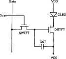
参照图1,子像素可以包括开关晶体管SWTFT,该开关晶体管SWTFT具有与扫描线Scan连接的栅极和与数据线Data连接的一端。而且,子像素可以包括驱动晶体管DRTFT,该驱动晶体管DRTFT具有与开关晶体管的另一端连接的栅极和与第二电源线VSS连接的一端。而且,子像素可以包括连接在驱动晶体管DRTFT的栅极与第二电源线VSS之间的电容器CST。此外,子像素可以包括有机发光二极管(OLED),该有机发光二极管(OLED)具有与第一电源线VDD连接的阳极和与驱动晶体管DRTFT的另一端连接的阴极。Referring to FIG. 1 , the sub-pixel may include a switching transistor SWTFT having a gate connected to a scan line Scan and one end connected to a data line Data. Also, the sub-pixel may include a driving transistor DRTFT having a gate connected to the other end of the switching transistor and one end connected to the second power supply line VSS. Also, the sub-pixel may include a capacitor CST connected between the gate electrode of the driving transistor DRTFT and the second power supply line VSS. Also, the sub-pixel may include an organic light emitting diode (OLED) having an anode connected to the first power line VDD and a cathode connected to the other end of the driving transistor DRTFT.
例如,在根据本实施方式的有机发光显示器件中,N型晶体管用作子像素中的开关晶体管SWTFT和驱动晶体管DRTFT。For example, in the organic light emitting display device according to the present embodiment, N-type transistors are used as the switching transistor SWTFT and the driving transistor DRTFT in the sub-pixel.
当数据驱动器和扫描驱动器施加数据信号和扫描信号时,这种子像素结构使施加到第一电源线VDD的电流能流过第二电源线VSS。因此,该OLED发光,由此显示图像。This sub-pixel structure enables current applied to the first power supply line VDD to flow through the second power supply line VSS when the data driver and the scan driver apply data signals and scan signals. Accordingly, the OLED emits light, thereby displaying an image.
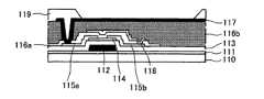
参照图2和图3,在基板110上设置缓冲层。该缓冲层111被形成为用来保护将在随后工序中形成的晶体管以使该晶体管免于受到从基板110流出的诸如碱离子(alkali ion)这样的杂质的影响。缓冲层111可由硅氧化物SiOx或硅氮化物SiNx形成。Referring to FIGS. 2 and 3 , a buffer layer is disposed on the
可以在缓冲层上设置栅极112。栅极112可由从钼Mo、铝Al、铬Cr、金Au、钛Ti、镍Ni、钕Nd、铜Cu和它们的合金组成的组中选出的一种形成。栅极112可以是单层,也可以是由从钼Mo、铝Al、铬Cr、金Au、钛Ti、镍Ni、钕Nd、铜Cu和它们的合金组成的组中选出的至少两种形成的多层。栅极还可以是钼Mo/铝Al-钕Nd或钼Mo/铝Al的双层。A
可以在栅极112上设置第一绝缘层113。第一绝缘层113可为由硅氧化物SiOx或硅氮化物SiNx形成的单层,或者可以是它们的多层。不过,第一绝缘层113并不限于此。A first
在第一绝缘层113上设置有源层114。有源层114可以包括非晶硅或多晶硅,多晶硅是被结晶化的非晶硅。尽管没有示出,但有源层114可以包括沟道区、源区和漏区。而且,有源层114可以包括用于减小接触电阻的欧姆接触层。The
可以在有源层114上设置漏极115a和源极115b。漏极115a和源极115b可形成为单层或多层。如果漏极115a和源极115b为单层,则漏极115a和源极115b可由从钼Mo、铝Al、铬Cr、金Au、钛Ti、镍Ni、钕Nd、铜Cu和它们的合金组成的组中选出的一种形成。如果漏极115a和源极115b为多层,则漏极115a和源极115b可以是Mo/Al-Nd或Mo/Al的双层,或Mo/Al-Nd/Mo的三层。A
可以在漏极115a和源极115b上设置第二绝缘层116a。第二绝缘层116a可以是硅氧化物SiOx层、硅氮化物SiNx层或它们的多层。不过,第二绝缘层116a并不限于此。第二绝缘层116a可以是钝化层。A second insulating
基板110上的栅极112、漏极115a和源极115b形成了驱动晶体管。驱动晶体管的漏极115a和源极115b之一可以与设置在第二绝缘层116a上的遮蔽金属(shield metal)118连接。遮蔽金属118防止晶体管的漏极115a和源极115b之间的干扰。根据晶体管的结构,遮蔽金属118可以省略。The
可以在第二绝缘层116a上设置第三绝缘层116b以提高平坦度(evenness)。第三绝缘层116b可以包括诸如聚酰亚胺这样的有机材料。The third
此前,描述了形成在基板110上的底栅型晶体管。不过,在基板110上不仅可以形成底栅型晶体管,也可以形成顶栅型晶体管。Heretofore, the bottom gate type transistor formed on the
可以在第三绝缘层116b上设置阴极117。阴极117可以与晶体管的漏极115a连接并分离地形成在每个子像素区域中。阴极117可由具有高反射率和低功函数的不透明材料形成。不过,阴极117并不限于此。A
可在阴极117的表面上进行等离子体预处理。用于等离子体预处理的气体可以包括O2、N2和Ar中的至少一种。Plasma pretreatment may be performed on the surface of
可以在阴极117上设置堤层(bank layer)119。堤层119包括暴露一部分阴极117的开口。堤层119可以包括诸如苯并环丁烯(BCB)树脂、丙烯酸树脂或聚酰亚胺树脂这样的有机材料。A
可以在由堤层119的开口暴露的阴极117上设置金属缓冲层120。金属缓冲层120可由铝Al、银Ag、钙Ca和镁Mg中的一种形成。不过,金属缓冲层120并不限于此。金属缓冲层120可由能够提高电子注入效率的任何金属材料形成。A
金属缓冲层120可以以大约

可以在金属缓冲层120上设置有机发光层121。有机发光层121可形成为根据一对应的子像素而发射红光、绿光和蓝光之一。根据有机发光层121的结构,还可以再有一发射白光的子像素。The organic
可以在有机发光层121上设置阳极122。阳极122可由诸如铟锡氧化物(ITO)、铟锌氧化物(IZO)、铟锡锌氧化物(ITZO)或Al2O3掺杂ZnO(AZO)这样的透明材料形成。不过,阳极122并不限于此。An
参照图4,有机发光层121可以设置在金属缓冲层120与阳极122之间。有机发光层121可以包括电子注入层121a、电子传输层121b、发光层121c、空穴传输层121d和空穴注入层121e。Referring to FIG. 4 , the organic
电子注入层121a使得电子的注入顺畅(smooth),其可由三(8-羟基喹啉)铝(tris(8-hydroxyquinolino)aluminum)(Alq3)、PBD、TAZ、螺环-PBD、BAlq、LiF或SAlq形成。不过,电子注入层121a并不限于此。The
电子传输层121b使得电子的传输顺畅,其可由Alq3(三(8-羟基喹啉)铝)、PBD、TAZ、螺环-PBD、BAlq、LiF或SAlq形成。不过,电子传输层121b并不限于此。The
发光层121c可以包括发射红光、绿光或蓝光的材料。发光层121c也可由磷光材料或荧光材料形成。不过,发光层121c并不限于此。The
如果发光层121c发红光,则发光层121c可由包括具有咔唑联苯(CBP)或1,3-双(咔唑-9-yl)mCP(1,3-bis(carbazol-9-yl)mCP)的主材料(host material)和具有由下述材料组成的组中的至少一种材料的掺杂物的磷光材料形成:PIQIr(acac)(双(1-苯基异喹啉)乙酰丙酮铱)(bis(1-phenylisoquinoline)acetylacetonate iridium)、PQIr(acac)(双(1-苯基喹啉)乙酰丙酮铱)(bis(1-phenylquinoline)acetylacetonate iridium)、PQIr(三(1-苯基喹啉)铱)(tris(1-phenylquinoline)iridium)、和PtOEP(八乙基卟啉铂)(octaethylporphyrin platinum)。发光层121c也可由具有PBD:Eu(DBM)3(Phen)或二萘嵌苯(Perylene)的荧光材料形成。不过,磷光材料和荧光材料不限于此。If the light-emitting
如果发光层121c发绿光,则发光层121c可由包括具有含CBP或mCP的主材料和含Ir(ppy)3(fac三(2-苯基吡啶)铱)(Ir(ppy)3(factris(2-phenylpyridine)iridium))的掺杂材料的磷光材料的材料形成。不同的是,发光层121c可由具有Alq3(三(8-羟基喹啉)铝)的荧光材料形成。不过,磷光材料和荧光材料不限于此。If the light-emitting
如果发光层121c发蓝光,则发光层121c可由包括主材料CBP或mCP以及具有(4,6-F2ppy)2Irpic的掺杂材料的磷光材料形成。不同的是,发光层121c可由具有从下述材料组成的组中选出的一种材料的荧光材料形成:螺环-DPVBi、螺环-6P、联苯乙烯苯(distyrylbenzene)(DSB)、联苯乙烯亚芳基(distyryl arylene)(DSA)、PFO聚合物和PPV聚合物。不过,磷光材料和荧光材料并不限于此。If the
空穴传输层121d使得空穴的传输顺畅。空穴传输层121d可由从下述材料组成的组中选出的一种材料形成:NPD(N,N-二萘基-N,N’-二苯基联苯胺)(N,N-dinaphthyl-N,N′-diphenyl benzidine)、TPD(N,N’-双-(3-甲基苯基)-N,N’-双-(苯基)-联苯胺)(N,N′-bis-(3-methylphenyl)-N,N′-bis-(phenyl)-benzidine)、s-TAD和MTDATA(4,4’,4”-三(N-3-甲基苯基-N-苯基-氨基)-三苯胺)(4,4′,4″-Tris(N-3-methylphenyl-N-phenyl-amino)-triphenylamine)。不过,空穴传输层121d并不限于此。The
空穴注入层121e使得空穴的注入顺畅。空穴注入层121e可由从下述材料组成的组中选出的一种材料形成:CuPc(酞菁铜)(cupper phthalocyanine)、PEDOT(聚(3,4)-乙烯基二氧噻吩)(poly(3,4)-ethylenedioxythiophene)、PANI(聚苯胺)(polyaniline)、和NPD(N,N-二萘基-N,N’-二苯基联苯胺)(N,N-dinaphthyl-N,N′-diphenyl benzidine)。不过,空穴注入层121e并不限于此。The
这里,本发明的实施方式并不限于图4。电子注入层121a、电子传输层121b、空穴传输层121d和空穴注入层121e中的至少一个可被省略。Here, the embodiment of the present invention is not limited to FIG. 4 . At least one of the
之后,将描述根据本发明一个实施方式的用于制造有机发光显示器件的方法。Afterwards, a method for manufacturing an organic light emitting display device according to an embodiment of the present invention will be described.
如图5和图6中所示,于如下的步骤S101在基板110上形成晶体管。As shown in FIGS. 5 and 6 , transistors are formed on the
制备基板110。为了在其上形成元件,可以选择由具有出色机械强度或优越尺寸稳定性的材料形成的基板。例如,基板110可由玻璃板、金属板、陶瓷板或塑料板(聚碳酸酯树脂、丙烯酸树脂、氯乙烯树脂、聚乙烯对苯二甲酸树脂(polyethylene terephthalate)、聚酰亚胺树脂、聚酯树脂、环氧树脂、硅树脂和含氟树脂(fluorine resin))形成。A
在基板110上形成缓冲层111。然后,在缓冲层111上形成栅极112。栅极112可为单层或多层。A
在栅极112上形成第一绝缘层113。第一绝缘层113可为硅氧化物(SiOx)层、硅氮化物(SiNx)层、或它们的多层。不过,第一绝缘层113并不限于此。A first insulating
在第一绝缘层113上形成有源层114。有源层114可以包括非晶硅或多晶硅,多晶硅是被结晶化的非晶硅。尽管没有示出,但有源层114可以包括沟道区、源区和漏区。有源层114也可以包括用于减小接触电阻的欧姆接触层。The
在有源层114上形成漏极115a和源极115b。漏极115a和源极115b可形成为单层或多层。A
在漏极115a和源极115b上形成第二绝缘层116a。第二绝缘层116a可以是由硅氧化物(SiOx)或硅氮化物(SiNx)构成的单层,或者可以是它们的多层。不过,第二绝缘层116a并不限于此。第二绝缘层116a可以是钝化层。A second insulating
为了提高平坦度,在第二绝缘层116a上形成第三绝缘层116b。第三绝缘层116b可以包括诸如聚酰亚胺这样的有机材料。In order to improve flatness, the third insulating
之前,对形成在基板110上的底栅型晶体管进行了描述。不过,在基板110上不仅可以形成底栅型晶体管,也可以形成顶栅型晶体管。同时,形成在基板110上的栅极112、漏极115a和源极115b形成驱动晶体管。驱动晶体管的漏极115a和源极115b之一可以与形成在第二绝缘层116a上的遮蔽金属118连接。Previously, the bottom gate type transistor formed on the
如图5和图6中所示,于如下的步骤S103在晶体管上形成阴极以使其与晶体管的漏极115a或源极连接。As shown in FIGS. 5 and 6 , a cathode is formed on the transistor so as to be connected to the
在晶体管的第三绝缘层116b上形成阴极117以使其与晶体管的漏极115a连接并在每个子像素区域处被隔离。阴极117可由诸如铝Al、铝合金(Al合金)或银(Ag)这样的具有高反射率的不透明材料形成。不过,阴极117并不限于此。A
如图5和6中所示,于如下的步骤S105在阴极117上形成具有开口的堤层119。As shown in FIGS. 5 and 6 , a
在阴极117上形成堤层119。堤层119包括暴露一部分阴极117的开口。堤层119可以包括诸如苯并环丁烯(BCB)树脂、丙烯酸树脂或聚酰亚胺树脂这样的有机材料。
如图5和图7中所示,于如下的步骤S107在阴极117上进行等离子体预处理。As shown in FIGS. 5 and 7 , plasma pretreatment is performed on the
使用等离子体对阴极117的表面进行预处理。用于预处理的等离子体气体包括氧气O2、氮气N2和氩气Ar中的至少一种。等离子体预处理移除自然形成在阴极117表面上的氧化层而且还抑制阴极表面的氧化。The surface of
如图5和图8中所示,于如下的步骤S109在阴极117上形成金属缓冲层120。As shown in FIGS. 5 and 8 , a
在通过堤层119的开口暴露的阴极117上形成金属缓冲层120。金属缓冲层120可以由铝Al、银Ag、钙Ca和镁Mg中的一种形成。不过,金属缓冲层120并不限于此。金属缓冲层120可由提高电子注入效率的任何金属材料形成。A
金属缓冲层120可以以大约


同时,可在同一腔室中连续进行等离子体预处理S107和金属缓冲层形成S109。因此,可提高量产性(yield rate)。Meanwhile, the plasma pretreatment S107 and the metal buffer layer formation S109 may be continuously performed in the same chamber. Therefore, the yield rate can be improved.
如图5和图9中所示,于如下的步骤S111在金属缓冲层120上形成有机发光层121。As shown in FIG. 5 and FIG. 9 , the organic
在金属缓冲层120上形成有机发光层121。有机发光层121形成为根据一对应的子像素而发射红光、绿光和蓝光之一。根据有机发光层121的结构,还可以再有一发射白光的子像素。The organic
如图5和图9中所示,于如下的步骤S113在有机发光层121上形成阳极122。As shown in FIGS. 5 and 9 , an
在有机发光层121上形成阳极122。阳极122可由诸如铟锡氧化物(ITO)、铟锌氧化物(IZO)、铟锡锌氧化物(ITZO)或者Al2O3掺杂ZnO(AZO)这样的透明材料形成。An
在进行了上述工序之后,形成了如图10中所示具有在基板110上以矩阵方式布置的多个子像素P的显示单元130。显示单元130中的多个子像素P可以包括如上所述的晶体管和有机发光二极管。After the above-described processes are performed, a
同时,形成在基板110上显示单元130上的多个子像素P对于湿气和氧气非常脆弱。因此,制备密封基板140,在显示单元130的基板110的外环处形成粘结部件150,并将基板110和密封基板140密封在一起。Meanwhile, the plurality of sub-pixels P formed on the
在密封之后,可以在基板110上形成具有数据驱动器和扫描驱动器的驱动单元160,基板上的驱动单元160可以与外部基板连接。尽管为了简便起见示意性地显示了驱动单元160,但驱动单元160的数据驱动器和扫描驱动器中的至少一个可形成在外部基板上。After sealing, a
如果通过驱动单元160施加驱动信号,则由根据本实施方式的方法制造的有机发光显示器件能够通过控制多个子像素P发光而显示图像。If a driving signal is applied through the driving
根据本实施方式的有机发光显示器件包括形成在阴极上的金属缓冲层以防止阴极氧化并提高电子注入效率。因此,根据本实施方式的有机发光显示器件具有提高的可靠性和延长的寿命。而且,根据本发明实施方式的制造有机发光显示器件的方法连续进行预处理阴极表面的工序和形成金属缓冲层的工序。因此,可提高量产性。The organic light emitting display device according to the present embodiment includes a metal buffer layer formed on a cathode to prevent oxidation of the cathode and improve electron injection efficiency. Therefore, the organic light emitting display device according to the present embodiment has improved reliability and extended lifetime. Also, the method of manufacturing an organic light emitting display device according to an embodiment of the present invention continuously performs the process of pretreating the surface of the cathode and the process of forming the metal buffer layer. Therefore, mass productivity can be improved.
前面的实施方式和优点仅仅是示例性的,并不解释为限制本发明。本教导能够很容易地应用于其他类型的装置。前面实施方式的描述意在用作说明,并不限制权利要求的范围。许多替换、修改和变化对于本领域技术人员来说是显而易见的。在所要求保护的技术方案中,手段加功能语句意在覆盖其中所描述的进行所述功能的结构,并且不仅覆盖结构上的等同物,还覆盖等同的结构。The foregoing embodiments and advantages are merely exemplary and are not to be construed as limiting the invention. The present teaching can be readily applied to other types of devices. The foregoing description of the embodiments is intended to be illustrative, and not to limit the scope of the claims. Many alternatives, modifications and variations will be apparent to those skilled in the art. In the claimed technical solutions, means-plus-function clauses are intended to cover the structures described therein that perform the described function, and not only structural equivalents, but also equivalent structures.
Claims (8)


Applications Claiming Priority (3)
| Application Number | Priority Date | Filing Date | Title |
|---|---|---|---|
| KR1020080079450 | 2008-08-13 | ||
| KR1020080079450AKR101352237B1 (en) | 2008-08-13 | 2008-08-13 | Organic Light Emitting Display and Manufacturing Method of the same |
| KR10-2008-0079450 | 2008-08-13 |
Publications (2)
| Publication Number | Publication Date |
|---|---|
| CN101651147A CN101651147A (en) | 2010-02-17 |
| CN101651147Btrue CN101651147B (en) | 2014-03-19 |
Family
ID=40937007
Family Applications (1)
| Application Number | Title | Priority Date | Filing Date |
|---|---|---|---|
| CN200910138472.2AActiveCN101651147B (en) | 2008-08-13 | 2009-05-18 | Organic light emitting display and manufacturing method of the same |
Country Status (4)
| Country | Link |
|---|---|
| US (1) | US8772074B2 (en) |
| KR (1) | KR101352237B1 (en) |
| CN (1) | CN101651147B (en) |
| GB (1) | GB2462504B (en) |
Families Citing this family (8)
| Publication number | Priority date | Publication date | Assignee | Title |
|---|---|---|---|---|
| KR101082254B1 (en)* | 2009-11-04 | 2011-11-09 | 삼성모바일디스플레이주식회사 | Organic light emitting display device and method of manufacturing the same |
| KR102081209B1 (en)* | 2013-03-26 | 2020-02-26 | 삼성디스플레이 주식회사 | Organic light emitting display device and manufacturing method thereof, and donor substrate, donor substrate set using manufacturing organic light emitting display device thereof |
| CN103400943B (en)* | 2013-08-07 | 2016-05-18 | 信利半导体有限公司 | Active matrix organic LED panel and preparation method thereof |
| KR101818907B1 (en) | 2014-11-27 | 2018-01-16 | 엘지디스플레이 주식회사 | Organic light emitting device, method for manufacturing organic light emitting device, and method for repairing of organic light emitting device |
| KR102617379B1 (en) | 2016-05-02 | 2023-12-27 | 삼성디스플레이 주식회사 | Organic light emitting display apparatus and manufacturing method thereof |
| KR20180076832A (en)* | 2016-12-28 | 2018-07-06 | 엘지디스플레이 주식회사 | Electroluminescent Display Device and Method of manufacturing the same |
| CN113224253B (en)* | 2020-06-12 | 2022-07-12 | 广东聚华印刷显示技术有限公司 | Display device and method of manufacturing the same |
| WO2022087903A1 (en)* | 2020-10-28 | 2022-05-05 | 京东方科技集团股份有限公司 | Light-emitting substrate and preparation method therefor, and light-emitting device |
Family Cites Families (19)
| Publication number | Priority date | Publication date | Assignee | Title |
|---|---|---|---|---|
| US5182000A (en)* | 1991-11-12 | 1993-01-26 | E. I. Du Pont De Nemours And Company | Method of coating metal using low temperature plasma and electrodeposition |
| GB2358284B (en)* | 1999-07-02 | 2004-07-14 | Hyundai Electronics Ind | Method of manufacturing capacitor for semiconductor memory device |
| TW540251B (en)* | 1999-09-24 | 2003-07-01 | Semiconductor Energy Lab | EL display device and method for driving the same |
| JP2001332741A (en)* | 2000-05-25 | 2001-11-30 | Sony Corp | Method for manufacturing thin film transistor |
| US7701130B2 (en)* | 2001-08-24 | 2010-04-20 | Semiconductor Energy Laboratory Co., Ltd. | Luminous device with conductive film |
| US7488986B2 (en)* | 2001-10-26 | 2009-02-10 | Semiconductor Energy Laboratory Co., Ltd. | Light emitting device |
| US6852997B2 (en)* | 2001-10-30 | 2005-02-08 | Semiconductor Energy Laboratory Co., Ltd. | Light emitting device |
| JP3823916B2 (en)* | 2001-12-18 | 2006-09-20 | セイコーエプソン株式会社 | Display device, electronic apparatus, and display device manufacturing method |
| CN1499643A (en) | 2002-11-11 | 2004-05-26 | 友达光电股份有限公司 | Active organic light emitting display and method of fabricating the same |
| JP4567962B2 (en)* | 2003-07-25 | 2010-10-27 | 三洋電機株式会社 | Electroluminescence element and electroluminescence panel |
| TWI238675B (en)* | 2004-01-19 | 2005-08-21 | Hitachi Displays Ltd | Organic light-emitting display and its manufacture method |
| JP4689176B2 (en)* | 2004-02-26 | 2011-05-25 | 大日本印刷株式会社 | Organic electroluminescence device |
| JP2005353577A (en)* | 2004-06-10 | 2005-12-22 | Samsung Sdi Co Ltd | Organic electroluminescent display device and manufacturing method thereof |
| KR100724483B1 (en)* | 2004-12-29 | 2007-06-04 | 엘지.필립스 엘시디 주식회사 | Organic light emitting display device and manufacturing method |
| KR100844788B1 (en)* | 2006-02-03 | 2008-07-07 | 주식회사 엘지화학 | Fabrication method for organic light emitting device and organic light emitting device fabricated by the same method |
| WO2007129874A1 (en)* | 2006-05-10 | 2007-11-15 | Lg Chem, Ltd. | Fabrication method for organic electronic device and organic electronic device fabricated by the same method |
| TWI308805B (en)* | 2006-09-22 | 2009-04-11 | Innolux Display Corp | Active matrix oled and fabricating method incorporating the same |
| JP4910780B2 (en)* | 2007-03-02 | 2012-04-04 | セイコーエプソン株式会社 | Organic electroluminescence device with input function and electronic device |
| KR100846968B1 (en)* | 2007-05-21 | 2008-07-17 | 삼성에스디아이 주식회사 | Organic light emitting display device |
- 2008
- 2008-08-13KRKR1020080079450Apatent/KR101352237B1/enactiveActive
- 2009
- 2009-05-18CNCN200910138472.2Apatent/CN101651147B/enactiveActive
- 2009-06-05GBGB0909753Apatent/GB2462504B/enactiveActive
- 2009-08-12USUS12/461,476patent/US8772074B2/enactiveActive
Also Published As
| Publication number | Publication date |
|---|---|
| KR101352237B1 (en) | 2014-01-16 |
| CN101651147A (en) | 2010-02-17 |
| US8772074B2 (en) | 2014-07-08 |
| US20100038643A1 (en) | 2010-02-18 |
| GB2462504A (en) | 2010-02-17 |
| GB2462504B (en) | 2011-09-14 |
| KR20100020724A (en) | 2010-02-23 |
| GB0909753D0 (en) | 2009-07-22 |
Similar Documents
| Publication | Publication Date | Title |
|---|---|---|
| US8003417B2 (en) | Organic electroluminescent display device and method of manufacturing the same | |
| KR102562897B1 (en) | Organic light emitting display device | |
| CN101651147B (en) | Organic light emitting display and manufacturing method of the same | |
| KR101888088B1 (en) | organic light emitting diode display device and method of manufacturing the same | |
| KR101365909B1 (en) | Organic Light Emitting Display and Manufactring Method of the same | |
| KR101679066B1 (en) | Organic Light Emitting Display Device and Fabricating Method thereof | |
| KR101572259B1 (en) | Manufacturing Method of Organic Light Emitting Display | |
| KR101577819B1 (en) | organic light emitting display | |
| KR101446344B1 (en) | Organic Light Emitting Display Device And Method For Manufacturing Of The Same | |
| KR101464752B1 (en) | Organic electroluminescent display device | |
| KR101678206B1 (en) | Organic Light Emitting Display Device | |
| KR101939798B1 (en) | Organic Light Emitting Display Device | |
| KR101572264B1 (en) | Organic Light Emitting Display Device and Manufacturing Method of the same | |
| KR101739127B1 (en) | Organic Light Emitting Display | |
| KR20100010816A (en) | Organic light emitting display and manufacturing method for the same | |
| KR20100071708A (en) | Thin film transistor substrate and organic light emitting display device using the same | |
| KR101613730B1 (en) | Organic Light Emitting Display Device and Manufacturing Method thereof | |
| KR20100013522A (en) | Manufacturing method for organic light emitting display | |
| KR101424272B1 (en) | Organic electroluminescence display device and manufacturing method thereof | |
| KR20100008179A (en) | Organic light emitting display and manufacturing method of the same | |
| KR20250104761A (en) | Display apparatus | |
| KR101475076B1 (en) | Organic electroluminescence display device and manufacturing method thereof | |
| KR20100006465A (en) | Organic light emitting display and manufacturing method for the same | |
| KR20100122277A (en) | Organic light emitting display device and manufacturing method of the same | |
| KR20110011078A (en) | Organic light emitting display device and manufacturing method thereof |
Legal Events
| Date | Code | Title | Description |
|---|---|---|---|
| C06 | Publication | ||
| PB01 | Publication | ||
| C10 | Entry into substantive examination | ||
| SE01 | Entry into force of request for substantive examination | ||
| GR01 | Patent grant | ||
| GR01 | Patent grant |