CN101651144B - Memory devices including vertical pillars and methods of manufacturing and operating same - Google Patents
Memory devices including vertical pillars and methods of manufacturing and operating sameDownload PDFInfo
- Publication number
- CN101651144B CN101651144BCN2009101669905ACN200910166990ACN101651144BCN 101651144 BCN101651144 BCN 101651144BCN 2009101669905 ACN2009101669905 ACN 2009101669905ACN 200910166990 ACN200910166990 ACN 200910166990ACN 101651144 BCN101651144 BCN 101651144B
- Authority
- CN
- China
- Prior art keywords
- gate
- substrate
- semiconductor
- vertical channel
- layer
- Prior art date
- Legal status (The legal status is an assumption and is not a legal conclusion. Google has not performed a legal analysis and makes no representation as to the accuracy of the status listed.)
- Active
Links
Images


Classifications
- H—ELECTRICITY
- H10—SEMICONDUCTOR DEVICES; ELECTRIC SOLID-STATE DEVICES NOT OTHERWISE PROVIDED FOR
- H10B—ELECTRONIC MEMORY DEVICES
- H10B41/00—Electrically erasable-and-programmable ROM [EEPROM] devices comprising floating gates
- H10B41/40—Electrically erasable-and-programmable ROM [EEPROM] devices comprising floating gates characterised by the peripheral circuit region
- H—ELECTRICITY
- H10—SEMICONDUCTOR DEVICES; ELECTRIC SOLID-STATE DEVICES NOT OTHERWISE PROVIDED FOR
- H10B—ELECTRONIC MEMORY DEVICES
- H10B43/00—EEPROM devices comprising charge-trapping gate insulators
- H10B43/20—EEPROM devices comprising charge-trapping gate insulators characterised by three-dimensional arrangements, e.g. with cells on different height levels
- H10B43/23—EEPROM devices comprising charge-trapping gate insulators characterised by three-dimensional arrangements, e.g. with cells on different height levels with source and drain on different levels, e.g. with sloping channels
- H10B43/27—EEPROM devices comprising charge-trapping gate insulators characterised by three-dimensional arrangements, e.g. with cells on different height levels with source and drain on different levels, e.g. with sloping channels the channels comprising vertical portions, e.g. U-shaped channels
- G—PHYSICS
- G11—INFORMATION STORAGE
- G11C—STATIC STORES
- G11C16/00—Erasable programmable read-only memories
- G11C16/02—Erasable programmable read-only memories electrically programmable
- G11C16/04—Erasable programmable read-only memories electrically programmable using variable threshold transistors, e.g. FAMOS
- G11C16/0408—Erasable programmable read-only memories electrically programmable using variable threshold transistors, e.g. FAMOS comprising cells containing floating gate transistors
- G—PHYSICS
- G11—INFORMATION STORAGE
- G11C—STATIC STORES
- G11C16/00—Erasable programmable read-only memories
- G11C16/02—Erasable programmable read-only memories electrically programmable
- G11C16/06—Auxiliary circuits, e.g. for writing into memory
- G11C16/10—Programming or data input circuits
- G11C16/14—Circuits for erasing electrically, e.g. erase voltage switching circuits
- G—PHYSICS
- G11—INFORMATION STORAGE
- G11C—STATIC STORES
- G11C16/00—Erasable programmable read-only memories
- G11C16/02—Erasable programmable read-only memories electrically programmable
- G11C16/06—Auxiliary circuits, e.g. for writing into memory
- G11C16/26—Sensing or reading circuits; Data output circuits
- H—ELECTRICITY
- H10—SEMICONDUCTOR DEVICES; ELECTRIC SOLID-STATE DEVICES NOT OTHERWISE PROVIDED FOR
- H10B—ELECTRONIC MEMORY DEVICES
- H10B41/00—Electrically erasable-and-programmable ROM [EEPROM] devices comprising floating gates
- H10B41/10—Electrically erasable-and-programmable ROM [EEPROM] devices comprising floating gates characterised by the top-view layout
- H—ELECTRICITY
- H10—SEMICONDUCTOR DEVICES; ELECTRIC SOLID-STATE DEVICES NOT OTHERWISE PROVIDED FOR
- H10B—ELECTRONIC MEMORY DEVICES
- H10B41/00—Electrically erasable-and-programmable ROM [EEPROM] devices comprising floating gates
- H10B41/20—Electrically erasable-and-programmable ROM [EEPROM] devices comprising floating gates characterised by three-dimensional arrangements, e.g. with cells on different height levels
- H10B41/23—Electrically erasable-and-programmable ROM [EEPROM] devices comprising floating gates characterised by three-dimensional arrangements, e.g. with cells on different height levels with source and drain on different levels, e.g. with sloping channels
- H10B41/27—Electrically erasable-and-programmable ROM [EEPROM] devices comprising floating gates characterised by three-dimensional arrangements, e.g. with cells on different height levels with source and drain on different levels, e.g. with sloping channels the channels comprising vertical portions, e.g. U-shaped channels
- H—ELECTRICITY
- H10—SEMICONDUCTOR DEVICES; ELECTRIC SOLID-STATE DEVICES NOT OTHERWISE PROVIDED FOR
- H10B—ELECTRONIC MEMORY DEVICES
- H10B41/00—Electrically erasable-and-programmable ROM [EEPROM] devices comprising floating gates
- H10B41/30—Electrically erasable-and-programmable ROM [EEPROM] devices comprising floating gates characterised by the memory core region
- H10B41/35—Electrically erasable-and-programmable ROM [EEPROM] devices comprising floating gates characterised by the memory core region with a cell select transistor, e.g. NAND
- H—ELECTRICITY
- H10—SEMICONDUCTOR DEVICES; ELECTRIC SOLID-STATE DEVICES NOT OTHERWISE PROVIDED FOR
- H10B—ELECTRONIC MEMORY DEVICES
- H10B43/00—EEPROM devices comprising charge-trapping gate insulators
- H10B43/10—EEPROM devices comprising charge-trapping gate insulators characterised by the top-view layout
- H—ELECTRICITY
- H10—SEMICONDUCTOR DEVICES; ELECTRIC SOLID-STATE DEVICES NOT OTHERWISE PROVIDED FOR
- H10B—ELECTRONIC MEMORY DEVICES
- H10B43/00—EEPROM devices comprising charge-trapping gate insulators
- H10B43/30—EEPROM devices comprising charge-trapping gate insulators characterised by the memory core region
- H10B43/35—EEPROM devices comprising charge-trapping gate insulators characterised by the memory core region with cell select transistors, e.g. NAND
- H—ELECTRICITY
- H10—SEMICONDUCTOR DEVICES; ELECTRIC SOLID-STATE DEVICES NOT OTHERWISE PROVIDED FOR
- H10D—INORGANIC ELECTRIC SEMICONDUCTOR DEVICES
- H10D30/00—Field-effect transistors [FET]
- H10D30/01—Manufacture or treatment
- H10D30/021—Manufacture or treatment of FETs having insulated gates [IGFET]
- H10D30/025—Manufacture or treatment of FETs having insulated gates [IGFET] of vertical IGFETs
- H—ELECTRICITY
- H10—SEMICONDUCTOR DEVICES; ELECTRIC SOLID-STATE DEVICES NOT OTHERWISE PROVIDED FOR
- H10D—INORGANIC ELECTRIC SEMICONDUCTOR DEVICES
- H10D30/00—Field-effect transistors [FET]
- H10D30/60—Insulated-gate field-effect transistors [IGFET]
- H10D30/68—Floating-gate IGFETs
- H10D30/681—Floating-gate IGFETs having only two programming levels
- H—ELECTRICITY
- H10—SEMICONDUCTOR DEVICES; ELECTRIC SOLID-STATE DEVICES NOT OTHERWISE PROVIDED FOR
- H10D—INORGANIC ELECTRIC SEMICONDUCTOR DEVICES
- H10D30/00—Field-effect transistors [FET]
- H10D30/60—Insulated-gate field-effect transistors [IGFET]
- H10D30/68—Floating-gate IGFETs
- H10D30/6891—Floating-gate IGFETs characterised by the shapes, relative sizes or dispositions of the floating gate electrode
- H10D30/6892—Floating-gate IGFETs characterised by the shapes, relative sizes or dispositions of the floating gate electrode having at least one additional gate other than the floating gate and the control gate, e.g. program gate, erase gate or select gate
- H—ELECTRICITY
- H10—SEMICONDUCTOR DEVICES; ELECTRIC SOLID-STATE DEVICES NOT OTHERWISE PROVIDED FOR
- H10D—INORGANIC ELECTRIC SEMICONDUCTOR DEVICES
- H10D30/00—Field-effect transistors [FET]
- H10D30/60—Insulated-gate field-effect transistors [IGFET]
- H10D30/69—IGFETs having charge trapping gate insulators, e.g. MNOS transistors
- H10D30/694—IGFETs having charge trapping gate insulators, e.g. MNOS transistors characterised by the shapes, relative sizes or dispositions of the gate electrodes
- H10D30/696—IGFETs having charge trapping gate insulators, e.g. MNOS transistors characterised by the shapes, relative sizes or dispositions of the gate electrodes having at least one additional gate, e.g. program gate, erase gate or select gate
- H—ELECTRICITY
- H10—SEMICONDUCTOR DEVICES; ELECTRIC SOLID-STATE DEVICES NOT OTHERWISE PROVIDED FOR
- H10D—INORGANIC ELECTRIC SEMICONDUCTOR DEVICES
- H10D62/00—Semiconductor bodies, or regions thereof, of devices having potential barriers
- H10D62/40—Crystalline structures
- H—ELECTRICITY
- H10—SEMICONDUCTOR DEVICES; ELECTRIC SOLID-STATE DEVICES NOT OTHERWISE PROVIDED FOR
- H10D—INORGANIC ELECTRIC SEMICONDUCTOR DEVICES
- H10D62/00—Semiconductor bodies, or regions thereof, of devices having potential barriers
- H10D62/80—Semiconductor bodies, or regions thereof, of devices having potential barriers characterised by the materials
- H10D62/83—Semiconductor bodies, or regions thereof, of devices having potential barriers characterised by the materials being Group IV materials, e.g. B-doped Si or undoped Ge
- H—ELECTRICITY
- H10—SEMICONDUCTOR DEVICES; ELECTRIC SOLID-STATE DEVICES NOT OTHERWISE PROVIDED FOR
- H10D—INORGANIC ELECTRIC SEMICONDUCTOR DEVICES
- H10D84/00—Integrated devices formed in or on semiconductor substrates that comprise only semiconducting layers, e.g. on Si wafers or on GaAs-on-Si wafers
- H10D84/01—Manufacture or treatment
- H10D84/0123—Integrating together multiple components covered by H10D12/00 or H10D30/00, e.g. integrating multiple IGBTs
- H10D84/0126—Integrating together multiple components covered by H10D12/00 or H10D30/00, e.g. integrating multiple IGBTs the components including insulated gates, e.g. IGFETs
- H10D84/0151—Manufacturing their isolation regions
- H—ELECTRICITY
- H10—SEMICONDUCTOR DEVICES; ELECTRIC SOLID-STATE DEVICES NOT OTHERWISE PROVIDED FOR
- H10D—INORGANIC ELECTRIC SEMICONDUCTOR DEVICES
- H10D84/00—Integrated devices formed in or on semiconductor substrates that comprise only semiconducting layers, e.g. on Si wafers or on GaAs-on-Si wafers
- H10D84/01—Manufacture or treatment
- H10D84/02—Manufacture or treatment characterised by using material-based technologies
- H10D84/03—Manufacture or treatment characterised by using material-based technologies using Group IV technology, e.g. silicon technology or silicon-carbide [SiC] technology
- H10D84/038—Manufacture or treatment characterised by using material-based technologies using Group IV technology, e.g. silicon technology or silicon-carbide [SiC] technology using silicon technology, e.g. SiGe
- H—ELECTRICITY
- H10—SEMICONDUCTOR DEVICES; ELECTRIC SOLID-STATE DEVICES NOT OTHERWISE PROVIDED FOR
- H10D—INORGANIC ELECTRIC SEMICONDUCTOR DEVICES
- H10D88/00—Three-dimensional [3D] integrated devices
Landscapes
- Engineering & Computer Science (AREA)
- Microelectronics & Electronic Packaging (AREA)
- Non-Volatile Memory (AREA)
- Semiconductor Memories (AREA)
- Chemical & Material Sciences (AREA)
- Crystallography & Structural Chemistry (AREA)
Abstract
Translated fromChinese
Description
Translated fromChinese技术领域technical field
本发明涉及一种半导体器件,尤其涉及一种包括竖直立柱的存储器件及制造和操作该存储器件的方法。The present invention relates to a semiconductor device, and more particularly, to a memory device including vertical pillars and methods of manufacturing and operating the memory device.
背景技术Background technique
随着高集成电子器件的持续关注,对于以更高速度和更低功率工作且具有增强的器件密度的半导体存储器件的需求从未停止。为了实现这一目标,已经开发出具有以水平和垂直阵列排列的晶体管单元的大规模多层器件。With the continuous focus on highly integrated electronic devices, there is never-ending demand for semiconductor memory devices operating at higher speeds and lower power with enhanced device densities. To achieve this goal, large-scale multilayer devices have been developed with transistor cells arranged in horizontal and vertical arrays.
在一种方式中,平面存储单元,例如NAND存储单元,以传统的水平阵列形成。然后将多个水平阵列沿竖直方向堆叠。由于为了实现最小的特征尺寸每一层都要进行严格的光刻步骤(lithography steps),这种方法有关的局限包括所得器件的低可靠性。另外,在这种配置中,用于驱动控制栅极的驱动晶体管的尺寸是影响层数的一个因素;因此,驱动晶体管的大小与层数的倍数成比例。这会带来集成问题和散热问题。In one approach, planar memory cells, such as NAND memory cells, are formed in a conventional horizontal array. Multiple horizontal arrays are then stacked vertically. Limitations associated with this approach include low reliability of the resulting devices due to the stringent lithography steps required for each layer in order to achieve the smallest feature size. Also, in this configuration, the size of the drive transistor used to drive the control gate is a factor affecting the number of layers; therefore, the size of the drive transistor is proportional to the multiple of the number of layers. This creates integration issues and thermal issues.
在另一种方法中,已开发出具有竖直定向的沟道(channel)的多层存储器件。在一种配置中,多个栅极层形成在基板上,且竖直(vertical)沟道贯穿该多个栅极层。在每条竖直沟道中,较低的栅极层被配置成用作下选择栅极,多个中间栅极层被配置为用作控制栅极,较高的栅极层被配置为用作上选择栅极。控制栅极可包括邻接竖直沟道的电荷存储层,从而该器件可用作非易失性存储器件。在第一水平方向上彼此相邻的上选择栅极被连接起来,用作器件的行选择线。在第二水平方向上彼此相邻的竖直沟道被连接起来,用作器件的位线。In another approach, multilayer memory devices with vertically oriented channels have been developed. In one configuration, a plurality of gate layers are formed on a substrate, and a vertical channel runs through the plurality of gate layers. In each vertical channel, the lower gate layer is configured as a lower select gate, the plurality of intermediate gate layers is configured as a control gate, and the upper gate layer is configured as a on the select gate. The control gate can include a charge storage layer adjacent to the vertical channel so that the device can be used as a non-volatile memory device. Upper select gates adjacent to each other in the first horizontal direction are connected to serve as row select lines of the device. Vertical channels adjacent to each other in the second horizontal direction are connected to serve as bit lines of the device.
试图采用竖直定向沟道的其它方法取得了有限的成功。在一种配置中,竖直沟道的底部连接到形成于基板中的公共源极扩散层。该公共源极扩散层被掺杂为具有n+掺杂(n+doping),且底层基板具有p型掺杂。从而,在公共源极扩散层和下面的基板间形成p-n结。竖直沟道被基板中的n+区域隔离;因此,难以通过任意电极控制竖直沟道的电势,而且有必要在控制栅极上施加负电压电平以擦除存储单元。这样的负电压电平将需要更复杂的器件电源电路,从而提高了器件成本。此外,施加负电压电平与传统的NAND存储器件的电源配置不一致,从而妨碍了以竖直定向的沟道存储器件直接替换传统的NAND器件。而且,当发生擦除操作时,擦除操作需要向邻接竖直沟道的控制栅极的电荷存储层注入空穴,竖直沟道中的空穴被向电荷存储层的注入耗尽。由于空穴的耗尽,竖直沟道的电势降低,使得擦除操作在一定时间内不够有效。Other approaches have attempted to employ vertically oriented channels with limited success. In one configuration, the bottoms of the vertical channels are connected to a common source diffusion layer formed in the substrate. The common source diffusion layer is doped with n+doping, and the underlying substrate has p-type doping. Thus, a p-n junction is formed between the common source diffusion layer and the underlying substrate. The vertical channel is isolated by the n+ region in the substrate; therefore, it is difficult to control the potential of the vertical channel through any electrode, and it is necessary to apply a negative voltage level on the control gate to erase the memory cell. Such negative voltage levels would require more complex device power supply circuitry, increasing device cost. Furthermore, applying negative voltage levels is inconsistent with the power supply configuration of conventional NAND memory devices, thereby preventing direct replacement of conventional NAND devices with vertically oriented trench memory devices. Furthermore, when an erase operation occurs, which requires the injection of holes into the charge storage layer adjacent to the control gate of the vertical channel, the holes in the vertical channel are depleted by the injection into the charge storage layer. Due to the depletion of holes, the potential of the vertical channel decreases, making the erasing operation not effective enough for a certain period of time.
为了防止竖直沟道中的空穴耗尽,已经提出了由栅极诱导的漏极漏损(gate-induced-drain-leakage,GIDL)操作进行的空穴注入,以便将竖直沟道的电势维持在适当的电平。然而,与直接衬底偏置(direct body biasing)比起来,通过GIDL效应进行的竖直沟道电势控制不是直截了当的,或者可能是不稳定的,这是由于它易于受结轮廓(junction profile)的影响,而这将导致被擦除的阈值电压分布退化(Vth distribution degradation)。此外,GIDL效应可能将热空穴注入结合到竖直沟道串中的下选择晶体管或边缘单元,这将使作为所得器件的耐久可靠性恶化。To prevent hole depletion in the vertical channel, hole injection by gate-induced-drain-leakage (GIDL) operation has been proposed so that the potential of the vertical channel maintained at an appropriate level. However, vertical channel potential control via the GIDL effect is not straightforward or may be unstable compared to direct body biasing due to its susceptibility to junction profile , which will lead to degradation of the erased threshold voltage distribution (Vth distribution degradation). Furthermore, the GIDL effect may inject hot holes into the lower selection transistors or edge cells incorporated in the vertical channel strings, which will deteriorate the endurance reliability of the resulting device.
发明内容Contents of the invention
本发明的实施例涉及竖直型半导体存储器件及制造该器件的方法。特别地,在特定的实施例,在包括半导体材料的接触区,半导体竖直沟道的底部直接连接到下面的基板。在特定的实施例,通过向竖直沟道的最低栅极施加合适的电压,在接触区形成反转层(inversion layer),以使该接触区成为导电的。该反转层进而操作为所得器件的公共源线。在竖直沟道和基板之间不存在扩散区域时,可以在所得器件中使用正的擦除电压来执行擦除操作,而不需要用于产生负电压的额外的电源电路。而且,由于正的擦除电压可被用于擦除操作,所以所得的器件与传统的水平配置的NAND存储器件是一致的;从而允许本发明的器件更直接替换这样的传统器件。Embodiments of the present invention relate to a vertical type semiconductor memory device and a method of manufacturing the same. In particular, in certain embodiments, the bottom of the semiconductor vertical channel is directly connected to the underlying substrate at a contact region comprising semiconductor material. In a specific embodiment, an inversion layer is formed in the contact region to render the contact region conductive by applying a suitable voltage to the lowest gate of the vertical channel. This inversion layer in turn operates as the common source line of the resulting device. In the absence of a diffusion region between the vertical channel and the substrate, a positive erase voltage can be used in the resulting device to perform an erase operation without the need for an additional power supply circuit for generating a negative voltage. Furthermore, since a positive erase voltage can be used for the erase operation, the resulting device is consistent with conventional horizontally configured NAND memory devices; thereby allowing the device of the present invention to more directly replace such conventional devices.
在一个方案中,半导体器件包括:在水平方向延伸的由半导体材料制成的基板;在该基板上的多个层间电介质层;多个栅极图案,每个栅极图案位于相邻的较低层间电介质层与相邻的较高层间电介质层之间;以及在竖直方向延伸穿过该多个层间电介质层和该多个栅极图案的由半导体材料制成的竖直沟道,其中在每个栅极图案和竖直沟道间具有使栅极图案与竖直沟道绝缘的栅极绝缘层,竖直沟道在包括半导体区的接触区接触基板。In one aspect, a semiconductor device includes: a substrate made of a semiconductor material extending in a horizontal direction; a plurality of interlayer dielectric layers on the substrate; a plurality of gate patterns, each of which is located at an adjacent Between the lower interlayer dielectric layer and the adjacent higher interlayer dielectric layer; and vertical channels made of semiconductor material extending in the vertical direction through the plurality of interlayer dielectric layers and the plurality of gate patterns , wherein there is a gate insulating layer insulating the gate pattern from the vertical channel between each gate pattern and the vertical channel, and the vertical channel contacts the substrate at a contact region including a semiconductor region.
在一个实施例中,接触区包括基板的上表面和竖直沟道的下部分,且其中基板的上表面和竖直沟道的下部分的至少侧壁包括半导体区。In one embodiment, the contact region includes an upper surface of the substrate and a lower portion of the vertical channel, and wherein at least sidewalls of the upper surface of the substrate and the lower portion of the vertical channel include a semiconductor region.
在另一个实施例中,当在该接触区施加产生反转区的电压时,该接触区是导电的。In another embodiment, the contact region is conductive when a voltage is applied across the contact region that produces an inversion region.
在另一个实施例中,半导体器件包括半导体存储器件,且其中:多个栅极图案中最高的(upper-most)栅极图案包括上选择晶体管的上选择栅极,多个栅极图案中最低的(lower-most)栅极图案包括下选择晶体管的下选择栅极;多个栅极图案中在上选择栅极和下选择栅极之间的剩余栅极图案包括半导体器件的共同串(common string)的存储单元晶体管的控制栅极;并且进一步包括:在下选择栅极和基板之间的多个层间电介质层中的最低(lower-most)层间电介质层,该最低层间电介质层具有第一厚度,且其中在控制栅极之间的层间电介质层具有第二厚度,其中该第一厚度小于该第二厚度;并且其中选择该第一厚度以使得施加到下选择栅极的电压在接触区产生导致该接触区导电的反转层。In another embodiment, the semiconductor device includes a semiconductor memory device, and wherein: the upper-most gate pattern of the plurality of gate patterns includes an upper select gate of the upper select transistor, and the lowest of the plurality of gate patterns The lower-most gate pattern includes the lower selection gate of the lower selection transistor; the remaining gate patterns between the upper selection gate and the lower selection gate among the plurality of gate patterns include a common string (common string) of semiconductor devices. string) of the memory cell transistor; and further comprising: a lower-most (lower-most) interlayer dielectric layer among a plurality of interlayer dielectric layers between the lower select gate and the substrate, the lowest interlayer dielectric layer having A first thickness, and wherein the interlayer dielectric layer between the control gates has a second thickness, wherein the first thickness is less than the second thickness; and wherein the first thickness is selected such that the voltage applied to the lower select gate An inversion layer is created in the contact area which causes the contact area to conduct.
在另一个实施例中,竖直沟道的半导体材料选自由单晶半导体材料和多晶半导体材料组成的组。In another embodiment, the semiconductor material of the vertical channel is selected from the group consisting of single crystal semiconductor material and polycrystalline semiconductor material.
在另一个实施例中,基板的半导体材料选自由单晶半导体材料和多晶半导体材料组成的组。In another embodiment, the semiconductor material of the substrate is selected from the group consisting of monocrystalline semiconductor material and polycrystalline semiconductor material.
在另一个实施例中,栅极绝缘层包括电荷存储层,且其中半导体器件包括非易失性存储器件。In another embodiment, the gate insulating layer includes a charge storage layer, and wherein the semiconductor device includes a non-volatile memory device.
在另一个实施例中:多个栅极图案中最高的栅极图案包括上选择晶体管的上选择栅极;多个栅极图案中最低的栅极图案包括下选择晶体管的下选择栅极;多个栅极图案中在上选择栅极和下选择栅极之间的剩余栅极图案包括半导体器件的共同串的存储单元晶体管的控制栅极;存储单元晶体管的控制栅极被连接起来以提供半导体器件的字线,该存储单元晶体管共享在该半导体器件的水平方向布置的该器件的同一层;半导体器件的共同串的存储单元晶体管被竖直沟道串联耦接在一起;最高栅极图案被连接起来以提供上选择晶体管的上选择栅极,该最高栅极图案共享在半导体器件的第一水平方向布置的该器件的同一层;在半导体器件的第二水平方向布置的竖直沟道的上部分被连接起来,以提供该半导体器件的位线;并且该半导体器件包括半导体存储器件。In another embodiment: the highest gate pattern of the plurality of gate patterns includes an upper select gate of the upper select transistor; the lowest gate pattern of the plurality of gate patterns includes a lower select gate of the lower select transistor; The remaining gate patterns between the upper select gate and the lower select gate among the gate patterns comprise control gates of memory cell transistors of a common string of semiconductor devices; the control gates of the memory cell transistors are connected to provide semiconductor The word line of the device, the memory cell transistors share the same layer of the device arranged in the horizontal direction of the semiconductor device; the memory cell transistors of the common string of the semiconductor device are coupled together in series by the vertical channel; the highest gate pattern is connected to provide the upper select gate of the upper select transistor, the highest gate pattern sharing the same layer of the device arranged in a first horizontal direction of the semiconductor device; the vertical channel arranged in a second horizontal direction of the semiconductor device The upper portions are connected to provide bit lines of the semiconductor device; and the semiconductor device includes a semiconductor memory device.
在另一方案中,存储系统包括:产生命令和地址信号的存储控制器;以及包括多个存储器件的存储模块,该存储模块接收该命令和地址信号,并作为响应而向至少一个存储器件存储数据或者从至少一个存储器件取回(retrieve)数据。每个存储器件包括:在水平方向上延伸的由半导体材料制成的基板;在基板上的多个层间电介质层;多个栅极图案,每个栅极图案位于相邻的较低层间电介质层与相邻的较高层间电介质层之间;以及在竖直方向延伸穿过该多个层间电介质层和该多个栅极图案的由半导体材料制成的竖直沟道,其中在每个栅极图案和竖直沟道间具有使栅极图案与竖直沟道绝缘的栅极绝缘层,竖直沟道在包括半导体区的接触区接触基板。In another aspect, a memory system includes: a memory controller that generates command and address signals; and a memory module that includes a plurality of memory devices, the memory module receives the command and address signals, and in response stores data or retrieve data from at least one storage device. Each memory device includes: a substrate made of semiconductor material extending in the horizontal direction; a plurality of interlayer dielectric layers on the substrate; a plurality of gate patterns, each of which is located between adjacent lower layers Between the dielectric layer and the adjacent higher interlayer dielectric layer; and a vertical channel made of semiconductor material extending through the plurality of interlayer dielectric layers and the plurality of gate patterns in the vertical direction, wherein A gate insulating layer is provided between each gate pattern and the vertical channel to insulate the gate pattern from the vertical channel, and the vertical channel contacts the substrate at a contact region including a semiconductor region.
在一个实施例中,接触区包括基板的上表面和竖直沟道的下部分,且其中基板的上表面和竖直沟道下部分的至少侧壁包括半导体区域。In one embodiment, the contact region includes an upper surface of the substrate and a lower portion of the vertical channel, and wherein at least sidewalls of the upper surface of the substrate and the lower portion of the vertical channel include a semiconductor region.
在另一个实施例中,当在该接触区施加产生反转区的电压时,该接触区是导电的。In another embodiment, the contact region is conductive when a voltage is applied across the contact region that produces an inversion region.
在另一个实施例中,多个栅极图案中最高的栅极图案包括上选择晶体管的上选择栅极,多个栅极图案中最低的栅极图案包括下选择晶体管的下选择栅极;多个栅极图案中在上选择栅极和下选择栅极之间的剩余栅极图案包括半导体器件的共同串的存储单元晶体管的控制栅极;并且系统进一步包括:在下选择栅极和基板之间的栅极绝缘层,该栅极绝缘层具有第一厚度,且其中在控制栅极之间的层间电介质层具有第二厚度,其中该第一厚度小于该第二厚度;并且其中选择该第一厚度以使得施加到下选择栅极的电压在接触区产生导致该接触区导电的反转层。In another embodiment, the tallest gate pattern of the plurality of gate patterns includes an upper select gate of the upper select transistor, and the lowest gate pattern of the plurality of gate patterns includes a lower select gate of the lower select transistor; The remaining gate patterns between the upper select gate and the lower select gate among the gate patterns comprise control gates of memory cell transistors of a common string of semiconductor devices; and the system further includes: between the lower select gate and the substrate a gate insulating layer having a first thickness, and wherein the interlayer dielectric layer between the control gates has a second thickness, wherein the first thickness is smaller than the second thickness; and wherein the first thickness is selected A thickness such that a voltage applied to the lower select gate creates an inversion layer at the contact region that causes the contact region to conduct.
在另一个实施例中,栅极绝缘层包括电荷存储层,且其中半导体器件包括非易失性存储器件。In another embodiment, the gate insulating layer includes a charge storage layer, and wherein the semiconductor device includes a non-volatile memory device.
在另一个实施例中:多个栅极图案中最高的栅极图案包括上选择晶体管的上选择栅极;多个栅极图案中最低的栅极图案包括下选择晶体管的下选择栅极;多个栅极图案中在上选择栅极和下选择栅极之间的剩余栅极图案包括半导体器件的共同串的存储单元晶体管的控制栅极;存储单元晶体管的控制栅极被连接起来以提供半导体器件的字线,该存储单元晶体管共享在半导体器件的水平方向布置的该器件的同一层;半导体器件的共同串的存储单元晶体管被竖直沟道串联耦接在一起;最高栅极图案被连接起来以提供上选择晶体管的上选择栅极,该最高栅极图案共享在半导体器件的第一水平方向布置的该器件的同一层;并且在半导体器件的第二水平方向布置的竖直沟道的上部分被连接起来,以提供该半导体器件的位线。In another embodiment: the highest gate pattern of the plurality of gate patterns includes an upper select gate of the upper select transistor; the lowest gate pattern of the plurality of gate patterns includes a lower select gate of the lower select transistor; The remaining gate patterns between the upper select gate and the lower select gate among the gate patterns comprise control gates of memory cell transistors of a common string of semiconductor devices; the control gates of the memory cell transistors are connected to provide semiconductor The word line of the device, the memory cell transistors sharing the same layer of the device arranged in the horizontal direction of the semiconductor device; the memory cell transistors of the common string of the semiconductor device are coupled together in series by the vertical channel; the highest gate pattern is connected rise to provide the upper select gate of the upper select transistor, the highest gate pattern sharing the same layer of the device arranged in a first horizontal direction of the semiconductor device; and the vertical channel arranged in a second horizontal direction of the semiconductor device The upper portions are connected to provide bit lines of the semiconductor device.
在另一方面,一种制造半导体器件的方法包括:提供在水平方向延伸的由半导体材料制成的基板;提供在该基板上的多个层间电介质层;提供多个栅极图案,每个栅极图案位于相邻的较低层间电介质层与相邻的较高层间电介质层之间;提供在竖直方向延伸穿过该多个层间电介质层和该多个栅极图案的由半导体材料制成的竖直沟道;并且在每个栅极图案和竖直沟道间提供使栅极图案与竖直沟道绝缘的栅极绝缘层,其中竖直沟道在包括半导体区的接触区接触基板。In another aspect, a method of manufacturing a semiconductor device includes: providing a substrate made of a semiconductor material extending in a horizontal direction; providing a plurality of interlayer dielectric layers on the substrate; providing a plurality of gate patterns, each The gate pattern is located between the adjacent lower interlayer dielectric layer and the adjacent upper interlayer dielectric layer; a semiconductor layer extending through the plurality of interlayer dielectric layers and the plurality of gate patterns in the vertical direction is provided. a vertical channel made of material; and a gate insulating layer for insulating the gate pattern from the vertical channel is provided between each gate pattern and the vertical channel, wherein the vertical channel is at a contact including a semiconductor region area in contact with the substrate.
在一个实施例中,接触区包括基板的上表面和竖直沟道的下部分,且其中基板的上表面和竖直沟道的下部分的至少侧壁包括半导体区域。In one embodiment, the contact region includes an upper surface of the substrate and a lower portion of the vertical channel, and wherein at least sidewalls of the upper surface of the substrate and the lower portion of the vertical channel include a semiconductor region.
在另一个实施例中,当在该接触区施加致使产生反转区的电压时,该接触区是导电的。In another embodiment, the contact region is conductive when a voltage is applied across the contact region that causes an inversion region.
在另一个实施例中,半导体器件包括半导体存储器件,且其中:多个栅极图案中最高的栅极图案包括上选择晶体管的上选择栅极,多个栅极图案中最低的栅极图案包括下选择晶体管的下选择栅极;多个栅极图案中在上选择栅极和下选择栅极之间的剩余栅极图案包括半导体器件的共同串的存储单元晶体管的控制栅极;并且方法进一步包括:在下选择栅极和基板之间提供多个层间电介质层中的最低层间电介质层,该最低层间电介质层具有第一厚度,且其中在控制栅极之间的层间电介质层具有第二厚度,其中该第一厚度小于该第二厚度;并且其中选择该第一厚度以使得施加到下选择栅极的电压在接触区产生导致该接触区导电的反转层。In another embodiment, the semiconductor device includes a semiconductor memory device, and wherein: the tallest gate pattern of the plurality of gate patterns includes an upper select gate of the upper select transistor, and the lowest gate pattern of the plurality of gate patterns includes a lower selection gate of the lower selection transistor; a remaining gate pattern between the upper selection gate and the lower selection gate among the plurality of gate patterns comprises a control gate of a memory cell transistor of a common string of semiconductor devices; and the method further comprising: providing a lowest interlayer dielectric layer of a plurality of interlayer dielectric layers between the lower select gate and the substrate, the lowest interlayer dielectric layer having a first thickness, and wherein the interlayer dielectric layer between the control gates has a second thickness, wherein the first thickness is less than the second thickness; and wherein the first thickness is selected such that a voltage applied to the lower select gate creates an inversion layer at the contact region that causes the contact region to conduct.
在另一个实施例中,栅极绝缘层包括电荷存储层,且其中半导体器件包括非易失性存储器件。In another embodiment, the gate insulating layer includes a charge storage layer, and wherein the semiconductor device includes a non-volatile memory device.
在另一方案中,提供一种在半导体存储器件上执行擦除操作的方法,该半导体存储器件包括:在水平方向延伸的由半导体材料制成的基板;在该基板上的多个层间电介质层;多个栅极图案,每个栅极图案位于相邻的较低层间电介质层与相邻的较高层间电介质层之间;以及在竖直方向延伸穿过该多个层间电介质层和该多个栅极图案的由半导体材料制成的竖直沟道,其中在每个栅极图案和竖直沟道间具有使栅极图案与竖直沟道绝缘的栅极绝缘层,竖直沟道在包括半导体材料的接触区接触基板,其中:多个栅极图案中最高的栅极图案包括上选择晶体管的上选择栅极;多个栅极图案中最低的栅极图案包括下选择晶体管的下选择栅极;多个栅极图案中在上选择栅极和下选择栅极之间的剩余栅极图案包括半导体器件的共同串的存储单元晶体管的控制栅极;存储单元晶体管的控制栅极被连接起来以提供半导体器件的字线,该存储单元晶体管共享在半导体器件的水平方向布置的该器件的同一层;半导体器件的共同串的存储单元晶体管被竖直沟道串联耦接在一起;最高栅极图案被连接起来以提供上选择晶体管的上选择栅极,该最高栅极图案共享在半导体器件的第一水平方向布置的该器件的同一层;并且在半导体器件的第二水平方向布置的竖直沟道的上部分被连接起来,以提供该半导体器件的位线。擦除操作包括:将共同串的下选择栅极和上选择栅极置于浮置状态;向字线施加接地电压或正电压;向半导体基板施加正的擦除电压。In another aspect, there is provided a method of performing an erase operation on a semiconductor memory device including: a substrate made of a semiconductor material extending in a horizontal direction; a plurality of interlayer dielectrics on the substrate layer; a plurality of gate patterns, each gate pattern being located between an adjacent lower interlayer dielectric layer and an adjacent upper interlayer dielectric layer; and extending through the plurality of interlayer dielectric layers in a vertical direction and vertical channels made of a semiconductor material of the plurality of gate patterns, wherein a gate insulating layer is provided between each gate pattern and the vertical channels to insulate the gate patterns from the vertical channels, the vertical channels The straight channel contacts the substrate at a contact region comprising a semiconductor material, wherein: a tallest gate pattern of the plurality of gate patterns comprises an upper select gate of an upper select transistor; a lowest gate pattern of the plurality of gate patterns comprises a lower select gate A lower selection gate of a transistor; a remaining gate pattern between an upper selection gate and a lower selection gate among a plurality of gate patterns; a control gate of a memory cell transistor of a common string of semiconductor devices; a control gate of the memory cell transistor The gates are connected to provide a word line of the semiconductor device, the memory cell transistors sharing the same layer of the device arranged in the horizontal direction of the semiconductor device; the memory cell transistors of the common string of the semiconductor device are coupled in series by the vertical channel together; the uppermost gate pattern is connected to provide the upper selection gate of the upper selection transistor, the uppermost gate pattern sharing the same layer of the device arranged in the first horizontal direction of the semiconductor device; and in the second level of the semiconductor device Upper portions of the aligned vertical channels are connected to provide bit lines of the semiconductor device. The erasing operation includes: placing the lower selection gate and the upper selection gate of the common string in a floating state; applying a ground voltage or a positive voltage to the word line; and applying a positive erasing voltage to the semiconductor substrate.
在一个实施例中,接触区包括基板的上表面和竖直沟道的下部分,且其中基板的上表面和竖直沟道的下部分的至少侧壁包括半导体区域。In one embodiment, the contact region includes an upper surface of the substrate and a lower portion of the vertical channel, and wherein at least sidewalls of the upper surface of the substrate and the lower portion of the vertical channel include a semiconductor region.
在另一个实施例中,当在该接触区施加产生反转区的电压时,该接触区是导电的。In another embodiment, the contact region is conductive when a voltage is applied across the contact region that produces an inversion region.
在另一个实施例中,该方法进一步包括:在下选择栅极和基板之间提供多个层间电介质层中的最低层间电介质层,该最低层间电介质层具有第一厚度,且其中在控制栅极之间的层间电介质层具有第二厚度,其中该第一厚度小于该第二厚度;并且其中选择该第一厚度以使得施加到该下选择栅极的电压在接触区产生导致该接触区导电的反转层。In another embodiment, the method further comprises: providing a lowermost interlayer dielectric layer of the plurality of interlayer dielectric layers between the lower select gate and the substrate, the lowermost interlayer dielectric layer having a first thickness, and wherein the control The interlayer dielectric layer between the gates has a second thickness, wherein the first thickness is less than the second thickness; and wherein the first thickness is selected such that a voltage applied to the lower select gate is generated at the contact region causing the contact region conductive inversion layer.
在另一方案中,提供一种在半导体存储器件上执行读操作的方法,该半导体存储器件包括:在水平方向上延伸的由半导体材料制成的基板;在该基板上的多个层间电介质层;多个栅极图案,每个栅极图案位于相邻的较低层间电介质层与相邻的较高层间电介质层之间;在竖直方向延伸穿过该多个层间电介质层和该多个栅极图案的由半导体材料制成的竖直沟道,其中在每个栅极图案和竖直沟道间具有使栅极图案与竖直沟道绝缘的栅极绝缘层,竖直沟道在包括半导体区的接触区接触基板;其中:多个栅极图案中最高的栅极图案包括上选择晶体管的上选择栅极;多个栅极图案中最低的栅极图案包括下选择晶体管的下选择栅极;多个栅极图案中在上选择栅极和下选择栅极之间的剩余栅极图案包括半导体器件的共同串的存储单元晶体管的控制栅极;存储单元晶体管的控制栅极被连接起来以提供半导体器件的字线,该存储单元晶体管共享在半导体器件的水平方向布置的该器件的同一层;半导体器件的共同串的存储单元晶体管被竖直沟道串联耦接在一起;最高栅极图案被连接起来以提供上选择晶体管的上选择栅极,该最高栅极图案共享在半导体器件的第一水平方向布置的该器件的同一层;在半导体器件的第二水平方向布置的竖直沟道的上部分被连接起来,以提供该半导体器件的位线。读操作包括:向半导体基板施加接地电压;向共同串的未选择存储单元晶体管的控制栅极施加读电压;向共同串的被选择的上选择晶体管的栅极施加读电压;向共同串的被选择的存储单元晶体管的控制栅极施加标准电压(criterionvoltage);向共同串及相邻串的下选择晶体管的下选择栅极施加读电压,从而在接触区中在半导体基板的较高区域和竖直沟道的至少侧壁的较低区域产生导电反转层,在读操作期间,该反转层作为半导体存储器件的导电的公共源线而操作。In another aspect, there is provided a method of performing a read operation on a semiconductor memory device comprising: a substrate made of a semiconductor material extending in a horizontal direction; a plurality of interlayer dielectrics on the substrate layer; a plurality of gate patterns, each gate pattern being located between an adjacent lower interlayer dielectric layer and an adjacent upper interlayer dielectric layer; extending in a vertical direction through the plurality of interlayer dielectric layers and The plurality of gate patterns are vertical channels made of semiconductor material, wherein there is a gate insulating layer between each gate pattern and the vertical channel to insulate the gate pattern from the vertical channel, vertically The channel contacts the substrate at a contact region including a semiconductor region; wherein: the tallest gate pattern of the plurality of gate patterns includes an upper selection gate of the upper selection transistor; the lowest gate pattern of the plurality of gate patterns includes a lower selection transistor the lower selection gate of the plurality of gate patterns; the remaining gate pattern between the upper selection gate and the lower selection gate among the plurality of gate patterns includes the control gate of the memory cell transistor of the common string of the semiconductor device; the control gate of the memory cell transistor poles are connected to provide a word line of a semiconductor device, the memory cell transistors sharing the same layer of the device arranged in the horizontal direction of the semiconductor device; memory cell transistors of a common string of semiconductor devices are coupled together in series by a vertical channel the highest gate pattern is connected to provide the upper selection gate of the upper selection transistor, the highest gate pattern sharing the same layer of the device arranged in the first horizontal direction of the semiconductor device; arranged in the second horizontal direction of the semiconductor device Upper portions of the vertical channels are connected to provide bit lines of the semiconductor device. The read operation includes: applying a ground voltage to the semiconductor substrate; applying a read voltage to the control gates of the unselected memory cell transistors in the common string; applying a read voltage to the gates of the selected upper selection transistors in the common string; A criterion voltage is applied to the control gate of the selected memory cell transistor; a read voltage is applied to the lower selection gates of the lower selection transistors of the common string and the adjacent strings, so that in the contact area, the higher area and the vertical area of the semiconductor substrate The lower regions of at least the sidewalls of the straight channel create a conductive inversion layer that operates as a conductive common source line of the semiconductor memory device during a read operation.
在一个实施例中,接触区包括基板的上区域和竖直沟道的下部分,且其中基板的上表面和竖直沟道的下部分的至少侧壁包括半导体区域。In one embodiment, the contact region includes an upper region of the substrate and a lower portion of the vertical channel, and wherein at least sidewalls of the upper surface of the substrate and the lower portion of the vertical channel include a semiconductor region.
在另一个实施例中,该方法进一步包括:提供在下选择栅极和基板之间的多个层间电介质层中的最低层间电介质层,该最低层间电介质层具有第一厚度,且其中在控制栅极之间的层间电介质层具有第二厚度,其中该第一厚度小于该第二厚度;并且其中选择该第一厚度以使得施加到该下选择栅极的电压在接触区产生导致该接触区导电的反转层。In another embodiment, the method further comprises: providing a lowest interlayer dielectric layer of the plurality of interlayer dielectric layers between the lower select gate and the substrate, the lowest interlayer dielectric layer having a first thickness, and wherein the The interlayer dielectric layer between the control gates has a second thickness, wherein the first thickness is less than the second thickness; and wherein the first thickness is selected such that a voltage applied to the lower select gate is generated at the contact region causing the Inversion layer that conducts electricity in the contact area.
附图说明Description of drawings
通过对如在附图中所示的本发明优选实施例的更具体的描述,本发明实施例的以上及其它目的、特征和优点将更加明显,在附图中,在整个不同视图中,同样的标记符号指示相同的部件。附图无需被按比例绘制,相反,其重点于图示本发明的原理。在图中:The above and other objects, features and advantages of embodiments of the invention will be more apparent from a more particular description of preferred embodiments of the invention as shown in the accompanying drawings, in which, throughout the different views, also The reference symbols indicate the same parts. The drawings are not necessarily to scale, emphasis instead being placed upon illustrating the principles of the invention. In the picture:
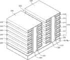
图1是依照本发明的实施例的竖直沟道存储器件的透视示意图;1 is a schematic perspective view of a vertical channel memory device according to an embodiment of the present invention;
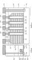
图2是依照本发明实施例的竖直沟道存储器件的顶部布局图;2 is a top layout diagram of a vertical channel memory device according to an embodiment of the present invention;
图3是依照本发明实施例的竖直沟道存储器件的剖面透视图;3 is a cross-sectional perspective view of a vertical channel memory device according to an embodiment of the present invention;
图4和图5是依照本发明实施例的图3的竖直沟道存储器件沿图2的断面线I-I’提取的剖面图;4 and 5 are cross-sectional views of the vertical channel memory device of FIG. 3 taken along the section line I-I' of FIG. 2 according to an embodiment of the present invention;
图6是依照本发明另一实施例的竖直沟道存储器件的透视示意图;6 is a schematic perspective view of a vertical channel memory device according to another embodiment of the present invention;
图7A是图6的竖直沟道存储器件的顶部布局图;7A is a top layout view of the vertical channel memory device of FIG. 6;
图7B是图6的竖直沟道存储器件的剖面透视图;7B is a cross-sectional perspective view of the vertical channel memory device of FIG. 6;
图8是依照本发明的实施例,示出访问单个存储单元的竖直沟道存储器件的透视示意图;8 is a schematic perspective view illustrating a vertical channel memory device accessing a single memory cell according to an embodiment of the present invention;
图9是依照本发明的实施例,示出在编程操作期间访问单个存储单元的竖直沟道存储器件的透视图;9 is a perspective view illustrating a vertical channel memory device accessing a single memory cell during a program operation, according to an embodiment of the present invention;
图10是依照本发明的实施例,示出擦除操作的竖直沟道存储器件的透视图;10 is a perspective view of a vertical channel memory device illustrating an erase operation according to an embodiment of the present invention;
图11是依照本发明的实施例,示出在读操作期间访问单个存储单元的竖直沟道存储器件的透视图;11 is a perspective view illustrating a vertical channel memory device accessing a single memory cell during a read operation, according to an embodiment of the present invention;
图12A-21A是依照本发明实施例的形成竖直沟道存储器件的方法的沿图2的断面线I-I’得到的剖面图,图12B-21B是依照本发明实施例的形成竖直沟道存储器件的方法的沿图2的断面线II-II’得到的剖面图;12A-21A are cross-sectional views taken along section line II' of FIG. 2 according to a method for forming a vertical channel memory device according to an embodiment of the present invention. A cross-sectional view of the method of the trench memory device along the section line II-II' of FIG. 2;
图22和23依照本发明的实施例的栅极绝缘层和竖直开口中立柱(pillar)的实施例的特写透视图;22 and 23 are close-up perspective views of an embodiment of a gate insulating layer and a pillar in a vertical opening in accordance with an embodiment of the present invention;
图24和25是依照本发明的另一实施例的形成竖直沟道存储器件的方法的剖面图;24 and 25 are cross-sectional views of a method of forming a vertical channel memory device according to another embodiment of the present invention;
图26-39是依照本发明的另一实施例的形成竖直沟道存储器件的方法的透视图;26-39 are perspective views of a method of forming a vertical channel memory device according to another embodiment of the present invention;
图40A-42A是依照本发明另一实施例的形成竖直沟道存储器件的方法的沿图2的断面线I-I’得到的剖面图,图40B-42B是依照本发明另一实施例的形成竖直沟道存储器件的方法的沿图2的断面线II-II’得到的剖面图;40A-42A are cross-sectional views taken along section line II' in FIG. 2 of a method for forming a vertical channel memory device according to another embodiment of the present invention, and FIGS. 40B-42B are cross-sectional views according to another embodiment of the present invention A cross-sectional view obtained along the section line II-II' of FIG. 2 according to the method for forming a vertical channel memory device;
图43是依照本发明的实施例的包括半导体器件的存储卡的模块图;43 is a block diagram of a memory card including a semiconductor device according to an embodiment of the present invention;
图44是依照本发明的实施例的使用存储模块(例如,在此所述类型的存储模块)的存储系统的模块图。44 is a block diagram of a memory system using a memory module (eg, a memory module of the type described herein) in accordance with an embodiment of the invention.
具体实施方式Detailed ways
现在,将参照附图在下文中将更全面地描述本发明的实施例,其中在附图中示出了本发明的优选实施例。然而,本发明可以不同形式实现,而不应被理解为只局限于这里所阐述的实施例。在整个说明书中,相同的数字指示相同的元件。Embodiments of the present invention will now be described more fully hereinafter with reference to the accompanying drawings, in which preferred embodiments of the invention are shown. However, the invention may be embodied in different forms and should not be construed as limited to the embodiments set forth herein. Throughout the specification, like numerals refer to like elements.
应该理解,尽管这里使用了术语第一、第二等来描述不同元件,但是这些元件不应受这些术语的限制。使用这些术语是用来将一个元件与另一元件区别开。例如,第一元件以被称为第二元件,并且,类似地,第二元件可以被称为第一元件,而不脱离本发明的范围。如这里所使用的,术语“和/或”包括相关的所列出项目的一个或多个的任意和全部组合。It will be understood that, although the terms first, second etc. are used herein to describe various elements, these elements should not be limited by these terms. These terms are used to distinguish one element from another. For example, a first element could be termed a second element, and, similarly, a second element could be termed a first element, without departing from the scope of the present invention. As used herein, the term "and/or" includes any and all combinations of one or more of the associated listed items.
应该理解,当元件被称为在另一元件“上”或者“连接到”或“耦接到”另一个元件时,该元件可以直接位于另一个元件上,或直接连接到或耦接到另一个元件,或者可以存在中间部件。相反,当元件被称为“直接在”另一个部件“上”,或“直接连接到”或“直接耦接到”另一个元件时,不存在中间元件。用于描述元件间关系的其它词汇也应以相同的方式来理解(例如,“在...之间”相对于“直接在...之间”,“邻接”相对于“直接邻接”,等等)。当元件被称为在另一个元件“上方”时,该元件可以在另一个元件的上方或下方,并且可以直接耦接到另一元件,或者可存在中间元件,或者元件被隔开一空隙(void)或间隙。It will be understood that when an element is referred to as being “on” or “connected to” or “coupled to” another element, it can be directly on the other element, or directly connected or coupled to the other element. One element, or there may be intermediate components. In contrast, when an element is referred to as being "directly on" or "directly connected to" or "directly coupled to" another element, there are no intervening elements present. Other words used to describe the relationship between elements should also be construed in a like fashion (e.g., "between" versus "directly between," "adjacent" versus "directly adjacent," etc). When an element is referred to as being "on" another element, the element can be above or below the other element, and can be directly coupled to the other element, or intervening elements may be present, or the elements may be separated by a gap ( void) or gap.
这里使用的术语只用于描述特定实施例,并不意欲限制本发明。如这里所使用的,单数形式也意欲包括复数形式,除非在上下文中以其它方式明示过。还应该理解,当这里使用术语“包括”、“包含”时,它们在详细说明所描述的特征、整数(integer)、步骤、操作、元件和/或组件的存在,但不排除存在或添加一个或多个其它特征、整数、步骤、操作、元件、组件和/或它们的组合。The terminology used herein is for describing particular embodiments only and is not intended to limit the invention. As used herein, singular forms are intended to include plural forms unless the context clearly dictates otherwise. It should also be understood that when the terms "comprising" and "comprising" are used here, they specify the existence of the described features, integers, steps, operations, elements and/or components, but do not exclude the existence or addition of an or multiple other features, integers, steps, operations, elements, components and/or combinations thereof.
图1是依照本发明的实施例的竖直沟道存储器件的透视示意图。FIG. 1 is a schematic perspective view of a vertical channel memory device according to an embodiment of the present invention.
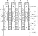
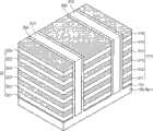
参见图1,在本例中,三维存储器件1000包括由虚线PL表示的多个竖直沟道或立柱。立柱PL在竖直方向上延伸,沿着共同的立柱形成的晶体管结合形成单元串(cell string)CSTR。单元串CSTR的最高(upper-most)晶体管被称为上选择晶体管,而单元串的最低(lower-most)晶体管被称为下选择晶体管。单元串CSTR中在上选择晶体管和下选择晶体管之间的晶体管包括该单元串CSTR的存储单元MC晶体管。Referring to FIG. 1 , in this example, a three-
在第一水平方向布置的立柱PL的顶部沿位线BL彼此连接。立柱PL的底部沿公共源线CSL彼此连接。立柱的底部还直接连接到基板阱Well。Tops of the pillars PL arranged in the first horizontal direction are connected to each other along the bit line BL. The bottoms of the columns PL are connected to each other along a common source line CSL. The bottom of the column is also directly connected to the substrate well Well.
沿第二水平方向布置的上选择晶体管的栅极沿上选择线USL彼此连接。下选择晶体管的栅极沿下选择板(select plate)LS_PT彼此连接,以提供下全局选择线(global select line)GLSL。共享同一共同竖直行的存储单元晶体管MC的栅极沿字线板(word line plates)WL_PT彼此连接,以提供全局字线(global word lines)GWL。不同行的全局字线GWL是独立的。Gates of the upper selection transistors arranged in the second horizontal direction are connected to each other along the upper selection line USL. Gates of the lower select transistors are connected to each other along a lower select plate LS_PT to provide a lower global select line GLSL. Gates of memory cell transistors MC sharing the same common vertical row are connected to each other along word line plates WL_PT to provide global word lines GWL. The global word lines GWL of different rows are independent.
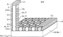
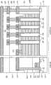
图2是依照本发明的实施例的竖直沟道存储器件的顶部布局视图。在本视图中,可以看出,栅极绝缘膜GI可设置成沿竖直立柱PL的竖直长度围绕该竖直立柱PL,从而将使该竖直立柱PL与上选择线USL、字线板WL_PT及下选择板LS_PT绝缘。从本视图中还可以看出,位线BL通过位线触点BL_CT来访问;字线板WL_PT通过字线触点WL_CT来访问;上选择线USL通过上选择线触点USL_CT来访问(access);公共源极线CSL,还在源区S处耦接到阱100/Well,通过源极触点S_CT来访问。FIG. 2 is a top layout view of a vertical channel memory device in accordance with an embodiment of the present invention. In this view, it can be seen that the gate insulating film GI may be arranged to surround the vertical column PL along its vertical length, thereby connecting the vertical column PL with the upper selection line USL, word line plate WL_PT and lower option board LS_PT are insulated. It can also be seen from this view that the bit line BL is accessed through the bit line contact BL_CT; the word line plate WL_PT is accessed through the word line contact WL_CT; the upper selection line USL is accessed through the upper selection line contact USL_CT (access) ; the common source line CSL, also coupled to the well 100/Well at the source region S, is accessed through the source contact S_CT.
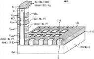
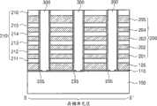
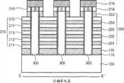
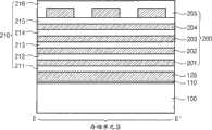
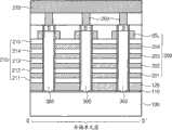
图3是依照本发明的实施例的竖直沟道存储器件的剖面透视图。参见图3,在本实施例中,提供半导体材料的基板100。在不同的实施例中,基板100可以包括以块状(bulk)或绝缘体上硅(SOI)配置的多晶或单晶半导体材料。基板100在水平方向延伸。下栅极绝缘层110在基板100上。在该下栅极绝缘层110上设置多个层间电介质层210(见图4)。设置字线板WL_PT和上选择线USL,每个都位于相邻的较低层间电介质层211、212、213、214、215...和相邻的较高层间电介质层211、212、213、214、215...之间。在最低的层间电介质层211和下栅极绝缘层110之间提供下选择板LS_PT。3 is a cross-sectional perspective view of a vertical channel memory device according to an embodiment of the present invention. Referring to FIG. 3 , in this embodiment, a
半导体材料的竖直立柱PL在竖直方向延伸穿过该多个层间电介质层210和下选择板LS_PT、字线板WL_PT及上选择线USL,从而竖直立柱PL至少部分地在水平方向被下选择板LS_PT、字线板WL_PT和上选择线USL围绕。例如,每个字线板WL_PT围绕或包围竖直立柱PL的壁的周界(perimeter)。下选择板LS_PT和上选择线USL同样如此。在下选择板LS_PT、字线板WL_PT和上选择线USL中的每一个与竖直立柱PL之间提供栅极绝缘膜GI。从本视图中还可以看出,每个竖直立柱PL包括沿其大部分长度的主体区B和在其顶部的漏区(drain region)D,漏区D与相应的位线BL接触。The vertical pillars PL of semiconductor material extend in the vertical direction through the plurality of interlayer
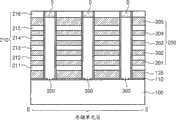
图4和图5是依照本发明实施例的图3的竖直沟道存储器件沿图2的断面线I-I’得到的剖面图。在图4中,可以看出,当适当的字线电压被施加到字线板WL_PT时,沿着竖直立柱的壁或外表面产生反转层(inversion layer)I。还可以看到,字线板WL_PT的厚度T1通常大于层间电介质层210的厚度T2。同时,可以看到,层间电介质层210的厚度T2大于电容电介质层CD的厚度T3。为了使电流沿立柱PL的竖直方向流动,在竖直立柱PL中产生且由相邻的字线板WL_PL所导致的反转层I应重叠(overlap)。该重叠或弥散场(fringing field)具有最大宽度W,或者在邻接的竖直立柱PL中在字线板WL_PT顶部表面水平(level)上方或在字线板WL_PT底部表面水平下方的竖直延伸量。4 and 5 are cross-sectional views of the vertical channel memory device of FIG. 3 taken along the section line I-I' of FIG. 2 according to an embodiment of the present invention. In FIG. 4, it can be seen that when an appropriate word line voltage is applied to the word line plate WL_PT, an inversion layer I is created along the walls or outer surfaces of the vertical pillars. It can also be seen that the thickness T1 of the word line plate WL_PT is generally greater than the thickness T2 of the
参见图5,可以看到,在每个立柱PL中,可以由源自下选择板LS_PT、字线板WL_PT或上选择线USL的弥散场FF产生扩散区效应(diffusionregion effect),而非对于每个存储单元晶体管使用源/漏扩散区。应用于传统平面NAND存储器件的弥散场的产生或操作已公开于申请号为2007/0205445的美国专利申请中,在此结合其全部内容作为参考。在竖直定向的存储器件的竖直沟道中形成源/漏区是有挑战性的。鉴于此,可以很方便地将弥散场配置应用于本发明实施例的方法和配置。Referring to FIG. 5, it can be seen that in each pillar PL, the diffusion region effect (diffusion region effect) can be generated by the fringe field FF originating from the lower selection plate LS_PT, the word line plate WL_PT or the upper selection line USL, rather than for each pillar PL. Each memory cell transistor uses source/drain diffusion regions. The generation or operation of fringing fields applied to conventional planar NAND memory devices is disclosed in US Patent Application No. 2007/0205445, the entire contents of which are incorporated herein by reference. Forming source/drain regions in vertical channels of vertically oriented memory devices is challenging. In view of this, it is convenient to apply the fringe field configuration to the method and configuration of the embodiment of the present invention.
图6是依照本发明另一实施例的竖直沟道存储器件的透视示意图。图7A是图6的竖直沟道存储器件的顶部布局图。图7B是图6的竖直沟道存储器件的剖面透视图。在本实施例中,可以看到,源接触插塞(source contact plug)S_CT可以由与基板阱100的掺杂类型不同的材料构成。例如,在所示的实施例中,阱100和竖直立柱PL由具有第一p-掺杂类型p-Si半导体材料形成,而源接触插塞S_CT由具有第二n-掺杂类型n+半导体材料形成。FIG. 6 is a schematic perspective view of a vertical channel memory device according to another embodiment of the present invention. FIG. 7A is a top layout view of the vertical channel memory device of FIG. 6 . FIG. 7B is a cross-sectional perspective view of the vertical channel memory device of FIG. 6 . In this embodiment, it can be seen that the source contact plug (source contact plug) S_CT may be composed of a material different from the doping type of the
图8是依照本发明的实施例的示出访问单个存储单元的竖直沟道存储器件的透视示意图。在本实施例中,可以看出,通过向所选字线WL、所选位线BL、下选择线LSL及所选上选择线USL施以适当的电压电平,可以访问三维阵列中的单个存储单元MC1来进行编程或读操作。8 is a schematic perspective view of a vertical channel memory device showing access to a single memory cell, according to an embodiment of the present invention. In this embodiment, it can be seen that by applying appropriate voltage levels to the selected word line WL, selected bit line BL, lower select line LSL, and selected upper select line USL, a single element in the three-dimensional array can be accessed. memory cell MC1 for programming or reading operations.
图9是依照本发明的实施例的竖直沟道存储器件的透视图,示出在编程操作期间访问单个存储单元。参见图9和下表1,在编程操作期间,向被选字线板Sel.WL_PT施以编程电压VPGM,并向未选的字线板Unsel.WL_PT施以通过电压(pass voltage)VPASS。向被选的位线Sel(BL)施以接地电压GND,并向未选的位线Unsel(BL)施以Vcc电压。向被选的上选择线USL施以Vcc电压,并向未选的上选择线USL施以GND电压。此外,向下选择线LSL施以GND电压,向公共源线CSL施以一电压(-),并向阱100施以GND电压。该操作导致电子在所选择的存储单元MC1的沟道中聚集,这将对所选择的存储单元MC1进行编程。可以使用自升压(self-boosting)技术的操作,例如在此结合作为参考的美国专利No.5,473,563中所描述的技术,来抑制对未选择立柱进行编程。自举操作阻止电流流向未选立柱。9 is a perspective view of a vertical channel memory device illustrating accessing a single memory cell during a programming operation, in accordance with an embodiment of the present invention. Referring to FIG. 9 and Table 1 below, during the programming operation, a programming voltageVPGM is applied to the selected word line board Sel.WL_PT, and a pass voltage (pass voltage) VPASS is applied to the unselected word line board Unsel.WL_PT. . The ground voltage GND is applied to the selected bit line Sel(BL), and the Vcc voltage is applied to the unselected bit line Unsel(BL). The Vcc voltage is applied to the selected upper selection line USL, and the GND voltage is applied to the unselected upper selection line USL. In addition, the GND voltage is applied to the lower selection line LSL, a voltage (−) is applied to the common source line CSL, and the GND voltage is applied to the
表1Table 1
图10是依照本发明的实施例的示出擦除操作的竖直沟道存储器件的透视图。参见图10及上表1,在擦除操作期间,向所选块(block)中的所有字线板WL_PT施以GND电压,并向所有位线BL和所有上选择线USL施以浮置电压(floating volatge)F。此外,向下选择线LSL和公共源线CSL施以浮置电压。向阱100施以正擦除电压VERS。该操作致使所有电子从阵列中的所有存储单元的沟道区移除,这将擦除阵列的存储单元。在这种情形下,由于在擦除操作期间将正擦除电压VERS直接传送到竖直立柱PL,所以通过向字线WL施以接地电压GND来擦除存储单元是可能的。而且,由于使用正擦除电压,且GND电压能被施加到字线WL,所以不必产生用于擦除操作的负电压。这将简化器件所需的电源供给电路,并且使所得器件与传统的水平配置的平面NAND存储器件的电源供给配置兼容;从而允许更方便地用依照本发明实施例配置的器件来更换这样的传统器件。FIG. 10 is a perspective view of a vertical channel memory device showing an erase operation according to an embodiment of the present invention. Referring to FIG. 10 and Table 1 above, during an erase operation, a GND voltage is applied to all word line plates WL_PT in a selected block, and a floating voltage is applied to all bit lines BL and all upper select lines USL (floating volatility) F. In addition, a floating voltage is applied to the down selection line LSL and the common source line CSL. A positive erase voltage VERS is applied to the
图11是依照本发明的实施例的示出在读操作期间访问单个存储单元的竖直沟道存储器件的透视图。参见图11和上表1,在读操作期间,向被选字线板Sel.WL_PT施以区分为‘1’和‘0’的标准电压,例如施加接地电压GND或者0V,并向未选字线板Unsel.WL_PT施以读电压VREAD。向被选位线Sel(BL)施以预充电电压Vpchg以区分‘1’和‘0’,并向未选位线Unsel(BL)施以GND电压。向被选的上选择线USL施以读电压VREAD,并向未选的上选择线USL施以GND电压。此外,向下选择线LSL施以读电压,向公共源线CSL施以GND电压,向阱100施以GND电压。11 is a perspective view of a vertical channel memory device illustrating accessing a single memory cell during a read operation, in accordance with an embodiment of the present invention. Referring to Figure 11 and Table 1 above, during the read operation, a standard voltage that is divided into '1' and '0' is applied to the selected word line board Sel.WL_PT, for example, the ground voltage GND or 0V is applied, and the unselected word line The board Unsel.WL_PT is supplied with a read voltage VREAD . A precharge voltage Vpchg is applied to the selected bit line Sel(BL) to distinguish between '1' and '0', and a GND voltage is applied to the unselected bit line Unsel(BL). The read voltage VREAD is applied to the selected upper selection line USL, and the GND voltage is applied to the unselected upper selection line USL. In addition, the read voltage is applied to the lower selection line LSL, the GND voltage is applied to the common source line CSL, and the GND voltage is applied to the
向下选择线LSL施以读电压VREAD导致竖直反转区504B沿着由半导体材料形成的竖直立柱PL的下部分的外壁形成。而且,由于在下选择线和阱100之间的下栅极绝缘体110相对较薄,所以水平反转区504A还在下栅极绝缘体110的下面沿着由半导体材料构成的阱的顶部形成。由于在沿着阱100的上部分以及沿着竖直立柱PL的下侧部分和上侧部分的半导体材料中形成的水平反转区504A和竖直反转区504B的存在,所以源区S和竖直立柱PL被电连接起来。以这种方式,水平反转区504A和竖直反转区504B操作为在读操作期间为阵列中的所有立柱提供公共源线CSL。Applying the read voltage VREAD to the down select line LSL causes the
在上面的图1中,与源极S相连的水平虚线表示由于在下选择板LS_PT上施加读电压VREAD而导致在阱的上部分的水平反转区504A的操作,而沿着竖直立柱PL的竖直虚线表示由于在下选择板LS_PT、字线板WL_PT和上选择线USL上施加读电压VREAD而导致在竖直立柱PL的侧壁的竖直反转区504B的操作。In FIG. 1 above, the horizontal dotted line connected to the source S indicates the operation of the
在上面的图6中,反转层的操作表现为多个MOS晶体管。比较起来,下选择板LS_PT提供栅极功能,下栅极绝缘层110提供氧化物的功能,而基板100提供半导体区域的功能。以这种方式,图6中的反转层的形成被表现为多个MOS晶体管,这些晶体管的栅极耦接到下选择板LS_PT。因此,当向下选择板LS_PT施以读电压VREAD时,水平反转层504A被激活。In Figure 6 above, the operation of the inversion layer appears as a plurality of MOS transistors. In comparison, the lower selection plate LS_PT provides a gate function, the lower
由于依照本发明的本实施例在编程、擦除和读操作期间施加到不同元件的电压与在那些相同操作期间施加到传统的水平设置的基于平面NAND的存储器件的电压类似,所以本发明实施例的器件与传统的基于NAND的存储器件的电源兼容,因而能够更加方便地替代传统器件用于采用该传统器件的系统中。本说明书实施例的配置和操作与最近提出的其它配置不同,最近提出的这些配置包括在序列号为No.2007/0252201的美国专利申请的公开文件中所提出的配置;在《VLSI技术论文的文摘专题集》(Symposium on VLSITechnology Digest of Technical Papers)(2007)的第14-15页记载的作者为H.Tanaka等人的“Bit Cost Scalable Technology with Punch and Plug Process forUltra High Density Flash Memory”一文中所提出的配置;以及在《IEDM技术文摘》(IEDM Technical Digest)(2007)的第449-452页记载的作者为Fukuzumi等人的“Optimal Integration and Characteristics of Vertical ArrayDevices for Ultra-High Density,Bit-Cost Scalable Flash Memory”一文中所提出的配置,在此结合这些文献中每一个的内容作为参考。在这些例子的每一个中,在形成于基板上区域中的扩散层中提供公共源线,作为基板的掺杂区。由此,在公共源扩散层与下面的基板之间形成p-n结。因此,难以通过任何电极来控制竖直沟道的电压,有必要在控制栅极上施加负电压电平来擦除存储单元。这样的负电压电平可能需要更复杂的器件电源电路,从而增加了器件成本。此外,施加负电压电平与传统NAND存储器件的电源配置不一致,从而阻碍了由竖直定向的沟道存储器件直接替换传统的NAND器件。如上所述,为了防止与在公共源线隔离的竖直沟道中的空穴耗尽相关的问题,提出了由栅极诱导的漏极漏(GIDL)操作进行的空穴注入,以便将竖直沟道的电势维持在适当的电平。然而,与直接主体偏置(direct body biasing)相比,通过GIDL效应进行的竖直沟道电压控制不简单,或者可能是不稳定的,这是因为它易于受结轮廓(junction profile)的影响,而这将导致被擦除的阈值电压分布退化(Vth distribution degradation)。此外,GIDL效应可能将热空穴注入合并到下选择晶体管或竖直沟道串中的边缘单元,这将使所得器件的耐久可靠性恶化。Since the voltages applied to the different elements during program, erase and read operations according to this embodiment of the invention are similar to the voltages applied to a conventional horizontally arranged planar NAND based memory device during those same operations, the present invention implements The device of the example is compatible with the power supply of the traditional NAND-based memory device, so it can more conveniently replace the traditional device and be used in the system using the traditional device. The configuration and operation of the embodiments of this specification differ from other recently proposed configurations, including those proposed in U.S. Patent Application Publication Serial No. 2007/0252201; "Bit Cost Scalable Technology with Punch and Plug Process for Ultra High Density Flash Memory" by H.Tanaka et al. proposed configuration; and "Optimal Integration and Characteristics of Vertical ArrayDevices for Ultra-High Density, Bit-High Density, Bit-High Density, Bit- Cost Scalable Flash Memory", the contents of each of these documents are incorporated herein by reference. In each of these examples, a common source line is provided in a diffusion layer formed in a region on the substrate as a doped region of the substrate. Thereby, a p-n junction is formed between the common source diffusion layer and the underlying substrate. Therefore, it is difficult to control the voltage of the vertical channel through any electrode, and it is necessary to apply a negative voltage level on the control gate to erase the memory cell. Such negative voltage levels may require more complex device power supply circuitry, increasing device cost. Furthermore, applying negative voltage levels is inconsistent with the power supply configuration of conventional NAND memory devices, thereby preventing direct replacement of conventional NAND devices by vertically oriented trench memory devices. As mentioned above, in order to prevent the problems associated with hole depletion in vertical channels isolated by a common source line, hole injection by gate-induced drain-drain (GIDL) operation is proposed so that the vertical The potential of the channel is maintained at an appropriate level. However, vertical channel voltage control via the GIDL effect is not straightforward or may be unstable compared to direct body biasing due to its susceptibility to junction profile , which will lead to degradation of the erased threshold voltage distribution (Vth distribution degradation). Furthermore, the GIDL effect may inject hot holes into the edge cells incorporated into the lower selection transistors or vertical channel strings, which would degrade the endurance reliability of the resulting device.
图12A-21A是依照本发明实施例的形成竖直沟道存储器件的方法的沿图2的断面线I-I’得到的剖面视图,图12B-21B是依照本发明实施例的形成竖直沟道存储器件的方法的沿图2的断面线II-II’得到的剖面视图。12A-21A are cross-sectional views taken along section line II' of FIG. 2 according to a method for forming a vertical channel memory device according to an embodiment of the present invention. A cross-sectional view of a method of a trench memory device taken along section line II-II' in FIG. 2 .
参见图12A和图12B,备好基板100。在一个实施例中,基板100包括为随后形成单晶竖直立柱PL提供籽晶层的单晶半导体材料基板。在另一个实施例中,基板100可以包括多晶半导体材料。依据传统技术,在基板的预定区域形成隔离区105。在基板上设置最低的层间电介质层110,这里也称为下栅极绝缘体110。在最低的层间电介质层110上形成第一下栅极层120,在该第一下栅极层120上形成第二下栅极层130。下栅极层120、130可选地可形成为单个栅极层或多个栅极层,如图所示。在下栅极层110包括多个栅极层的情形下,第一下栅极层120可以包括多晶硅层且第二下栅极层130可以包括金属层。在本发明的特定实施例中,最低的层间电介质层110足够薄,从而当向栅极层120、130施加适当的电压时,能够在基板100的底层半导体材料中产生反转层504A、504B(见上图11)。Referring to FIGS. 12A and 12B , a
参见图13A和图13B,在外围区域中构图第一下栅极层120和第二下栅极层130以形成下栅极图案125、135。依据传统的制造技术,可以使用下栅极图案125、135作为离子注入掩模,在外围区域形成源和漏区140。Referring to FIGS. 13A and 13B , the first
参见图14A和14B,在外围区域依次形成层间电介质层150和蚀刻终止层(etch stop layer)160。然后使用蚀刻终止层160作为蚀刻掩模去除在存储单元区域中的第二下栅极图案135。Referring to FIGS. 14A and 14B, an
参见图15A和图15B,在所得结构上的第一下栅极图案125上形成多个交替的层间电介质层210(在本例中包括层211、212、213、214、215和216)和导电栅极层200(在本例中包括层201、202、203、204和205)。在不同的实施例中,层间电介质层210可以包括选自由氧化物、HDP氧化物、CVD氧化物、PVD氧化物、BPSG、SOG及其混合物以及其它合适的材料所组成的组中的材料。栅极层200可以包括选自由多晶硅、W、TaN、TiN、金属硅化物及其混合物以及其它合适的材料所组成的组中的材料。15A and 15B, a plurality of alternating interlayer dielectric layers 210 (including
参见图16A和图16B,构图层间电介质层210和导电栅极层200以在存储单元区中形成竖直开口(opening)220。在外围区域,层间电介质层210和导电栅极层200被去除。在竖直开口220的底部,最低的层间电介质层110也被去除,从而在每个开口220中暴露基板100的顶部分。Referring to FIGS. 16A and 16B , the
参见图17A和图17B,在所得结构上提供栅极绝缘层230。栅极绝缘层230覆盖竖直开口220的底部和内侧壁以及存储单元区中最高的层间电介质层216的顶部,以及可选地覆盖外围区域中的蚀刻终止层160。Referring to FIGS. 17A and 17B , a
图22和图23是在竖直开口230中的栅极绝缘层和立柱的实施例的特写透视图。在一个实施例中,栅极绝缘层230包括电荷存储层,使得器件能够作为非易失性存储器件来操作。在图22和图23的例子中,栅极绝缘层230包括依次形成的阻挡绝缘层(blocking insulating layer)231、电荷存储层232和隧穿绝缘层(tunnel insulating layer)233。依照该配置形成的栅极绝缘层230在美国专利No.6,858,906和No.7,253,467以及美国专利申请No.2006/0180851中作了描述,在此结合其全部内容作为参考。在特定的实施例中,电荷存储层230可以包括电荷捕获层。在不同的实施例中,电荷捕获层可以包括SiN。用于电荷捕获层的其它合适的材料能采用,例如Al2O3、HfAlOx、HfAlON、HfSiOx、HfSiON及这些材料的多层。在另一实施例中,电荷存储层230可以包括浮置栅极层,其包括导电材料或半导体材料。22 and 23 are close-up perspective views of embodiments of gate insulating layers and posts in
参见图17A和图17B,在栅极绝缘层230上,在竖直开口220中形成间隔层(spacer layer)240。该间隔层240被各向异性蚀刻,以在开口220的底部暴露底层的栅极绝缘层230的中间部分。在立柱的形成期间,间隔层240用于在此后暴露下面的基板100期间沿着开口220的侧壁保护栅极绝缘层230,从而允许立柱PL与基板100直接接触。间隔层240优选由半导体材料如多晶硅、非晶硅或单晶硅形成,使得该材料与此后形成的立柱一致。以这种方式,不必在形成立柱PL之前去除间隔层240,而是可以保留下来以形成立柱PL的主体的一部分。Referring to FIGS. 17A and 17B , on the
参见图18A和图18B,使用间隔层240作为蚀刻掩模,去除栅极绝缘层230在开口220底部的被暴露的中间部分,暴露出下面的基板100。然后在开口220中形成立柱300。立柱300可以由半导体材料如多晶硅、非晶硅或单晶硅形成。Referring to FIGS. 18A and 18B , using the
在形成立柱300的一个实施例中,在开口220中形成多晶硅层或第一非晶硅层,与基板100的被暴露的上部分接触。在一个实施例中,可以由化学气相沉积(CVD)工艺来形成多晶硅层或非晶硅层;然而,可以应用形成多晶硅层或非晶硅层的其它合适的工艺。一个实施例中,在此阶段可以用杂质(impurities)掺杂多晶硅层或非晶硅层,例如用n-型杂质掺杂,使得所得的立柱300具有适当的掺杂特性。然后可以对多晶硅层或非晶硅层实施热处理,以将该层转换为单晶硅材料。在一个示例性实施例中,热处理可以采用激光诱导外延生长(LEG)工艺的形式来得到单晶硅材料,正如本领域所周知的。在可替代实施例中,可以使用选择性外延生长(SEG)工艺在开口220中从基板100的暴露的上表面生长出单晶硅立柱300。In one embodiment of forming the
在一个实施例中,用于形成立柱300的材料可以与用于形成间隔层240的材料相同。在其它实施例中,可以在形成立柱300之前去除间隔层240。此外,立柱300可以与基板100具有相同的掺杂剂类型(dopant type)。In one embodiment, the material used to form the
再参见图22和图23,立柱PL可以被形成为完全填充开口220,从而立柱PL为实心的,如在图22的实施例中所示。可替代地,立柱PL可以被形成为“通心型(macaroni-type)”立柱,其中立柱是中空形的,如在图23的实施例中所示,其具有底部和侧壁301A,以及中空的中间区域301B,或者,可替代地,由绝缘材料形成的中间区域301B。侧壁可以是柱状形状或矩形形状,并且可以完全围绕中间区域301B,或者可以与中间区域301B分隔开且位于中间区域301B的相反侧。Referring again to FIGS. 22 and 23 , the post PL may be formed to completely fill the
由半导体材料形成的所得立柱220在接触区域中与下面的基板/阱区域100直接接触。接触区域包括立柱220的下部分和基板100的上部分。由于它们直接接触,所以在立柱220和基板100之间不形成二极管型结(diode-typejunction)。这允许在读操作期间存在水平和竖直反转区504A、504B,如上图11中所示,从而能够访问单个存储单元。The resulting
参见图19A和图19B,还执行另外的构图,从而构图导电栅极层200(包括栅极层201、202、203、204和205的栅极线)以形成第一至第四字线板WL_PT和上选择线USL。如在图3中所示,栅极层200被构图成阶梯型(stair-type)图案以提供对该多个栅极层200的竖直访问。上选择线USL图案205每个均由接触插塞260A访问(access)。而且,在本实施例中,在器件的边缘区域,通过移除上选择线板USL、字线板WL_PT和下选择线板LS_PT的一部分,形成竖直开口以露出下面的基板100。然后,在所露出基板的顶部表面形成源区S,如图所示。接着,用填充开口的导电材料形成与下面的源区S相连的接触插塞260B。在器件的外围区域类似地形成接触插塞260C,以提供到外围晶体管的源/漏区140的连接。使用标准的掺杂技术在立柱300的顶部形成漏区D。该工艺导致在以上图2和图3的配置中所示类型的源接触插塞S_CT的形成。Referring to FIGS. 19A and 19B , additional patterning is also performed, thereby patterning the conductive gate layer 200 (including the gate lines of the gate layers 201, 202, 203, 204, and 205) to form first to fourth word line plates WL_PT and on select line USL. As shown in FIG. 3 , the
可替代地,源接触插塞S_CT可以与竖直立柱同时形成,例如,在以上图18A和图18B所示的形成立柱300的步骤期间。在该可替代实施例中,不必去除上选择线板USL、选择字线板WL_PT和下选择线板LS_PT的角落部分(corner portion),这是因为用于形成源触点S_CT的立柱是以与竖直立柱300相同的方式穿过这些板形成的。因此,形成在图7A和图7B的配置中所示类型的源接触插塞S_CT。Alternatively, the source contact plug S_CT may be formed simultaneously with the vertical stud, for example, during the step of forming the
参见图20A和图20B,第一导电层270形成于立柱300的漏区D上,且与立柱300的漏区D接触。然后,构图该第一导电层270、最高的层间电介质层216和最高的导电栅极层205以形成在第二水平方向延伸的上选择线USL图案205’。Referring to FIG. 20A and FIG. 20B , the first
参见图21A和图21B,进一步构图第一导电层270以在立柱300的漏极上提供焊盘276。在本例中,存储单元区中的接触插塞260A连接到外围区域中的接触插塞260C,从而将上选择线USL连接到外围区域中外围晶体管的相关源/漏区140。然后,在所得结构上形成第一上层间电介质层280,并且形成接触插塞285以与下面的导电部件接触,在该情形下,下面的导电部件为由第一导电层270形成的焊盘276。在第一上层间电介质层280上形成第二导电层,并构图该第二导电层以形成与下面的接触插塞285接触的导电线路290及特征(features)。在存储单元区,与布置在第一水平方向的竖直立柱的漏区D相连的导电线路提供器件的位线BL,如在图3中所示。然后,在所得结构上形成第二上层间电介质层292和接触插塞294,该接触插塞294形成为接触下面的导电部件,在该情形下,与最右边的特征290接触,进而接触与下面的源区S相连的源接触插塞260B。在第二上层间电介质层292上形成第三导电层,并构图该第三导电层以形成与下面的接触插塞260B相连的导电线路296。Referring to FIGS. 21A and 21B , the first
在上面的实施例中,由于同时形成,所以外围区域中晶体管的栅极绝缘层110和存储单元区的栅极绝缘层110具有同样的厚度。同时形成栅极绝缘层110提供了更有效的制造工艺,从而降低了制造成本。In the above embodiments, the
在上面的实施例中,在工艺的不同时期形成器件的外围区域晶体管的源/漏区140和存储单元区的源区S。例如,根据在图13A和图13B中所示的工艺步骤形成外围区域晶体管的源/漏区140,而根据在图19A和19B中所示的工艺步骤仅在形成源接触插塞260B的时间之前形成器件的存储单元区的源区。In the above embodiments, the source/
参见图24,在另一个实施例中,形成器件的存储单元区的公共源区S可以与外围区域晶体管的源/漏区140同时。例如,在构图外围晶体管的栅极图案125、135时,还可以在存储单元区的源区中构图栅极层,从而依照传统的制造技术,可以通过使用存储单元区中的下栅极图案125、135作为离子注入掩模在存储单元区中形成源区S。Referring to FIG. 24, in another embodiment, the common source region S of the memory cell region of the device may be formed at the same time as the source/
同样在上面的实施例中,存储单元区中的最低层间电介质层110(即,在形成下选择板LS_PT的下栅极图案125与基板之间的层间电介质层)的厚度与外围区域中下栅极绝缘层110(即,在外围区域中的栅极图案125、135与基板100之间的绝缘层)的厚度相同,这是因为在器件的外围和存储单元区中均最先形成层110以覆盖基板100。Also in the above embodiments, the thickness of the lowest
参见图25,在另一个实施例中,存储单元区中最低层间电介质层110’(即,在形成下选择板LS_PT的最低栅极图案125与基板之间的层间电介质层)的厚度可以不同于外围区域中下栅极绝缘层110(即,在外围区域中在栅极图案125、135与基板100之间的绝缘层)的厚度。在这种情形下,可以在形成第一和第二下栅极层图案125、125和125’之前,在不同时间形成层110’、110。而且,在需要时,层110’、110可以由不同的材料形成。Referring to FIG. 25, in another embodiment, the thickness of the lowest interlayer dielectric layer 110' in the memory cell region (ie, the interlayer dielectric layer between the
图26-图39是依照本发明另一实施例的形成竖直沟道存储器件的方法的透视图。26-39 are perspective views of a method of forming a vertical channel memory device according to another embodiment of the present invention.
参见图26,备好基板100。在一个实施例中,基板100包括为以后形成单晶竖直立柱PL提供籽晶层的单晶半导体材料基板。在另一个实施例中,基板包括多晶半导体材料。在基板上设置最低层间电介质层110。在本发明的特定实施例中,最低层间电介质层110足够薄,从而当向所得的最低栅极层LS_PT施加适当的电压时,能够在下面的基板100的半导体材料中产生反转层(见下图39)。在最低层间电介质层110上形成多个交替的层间电介质层210(在本例中包括层211、212、213、214、215和216)和多个牺牲层SC(在本例中包括层SC1、SC2、SC3、SC4、SC5和SC6)。在一个实施例中,层间电介质层210和牺牲层SC相对于彼此具有蚀刻选择性。例如,层间电介质层210可以包括氮化硅,而牺牲层SC可以包括氧化硅。在一个实施例中,牺牲层SC由易于被湿蚀刻工艺移除的材料形成。Referring to FIG. 26 , the
参见图27,第一线型(line-type)开口220被形成为在竖直方向穿过层间电介质层210、牺牲层SC和最低层间电介质层110,在水平方向间隔开,如图所示。该第一开口220暴露下面的基板100的上部分并在水平伸展(horizontal extension)的第一方向延伸。Referring to FIG. 27, a first line-
参见图28,在第一开口220的侧壁和底部形成半导体衬垫层(liner layer)300。然后,提供绝缘层310以填充第一开口220的剩余部分。半导体衬垫层将形成所得器件的竖直立柱PL,并且可以例如以上结合图18A和图18B所描述的方式来形成。在本示例中,示出了“通心”型立柱。参见上述图23的特写视图,“通心”型立柱PL包括环绕绝缘或中空内核301B的半导体材料301A的圆柱状壳体或侧壁。Referring to FIG. 28 , a
参见图29,在相邻的半导体衬垫300之间形成在第一水平方向延伸的多个第二开口225。在一个实施例中,第二开口120暴露最低层间电介质层110。该过程允许接近(access)一区域,在该区域处存储器件的所得栅极绝缘层230(见下图31)的控制栅极和浮置栅极将沿着所得半导体衬垫层300的侧壁形成,其中半导体衬垫层300的侧壁最终包括器件的竖直立柱。Referring to FIG. 29 , a plurality of
参见图30,通过湿刻工艺去除包括例如SC1、SC2、SC3、SC4、SC5和SC6的牺牲层图案SC。在其中最低层间电介质层110与牺牲层图案SC由相同材料形成的情形下,以同样方式去除该最低层间电介质层110的暴露部分。在牺牲层图案SC由氮化硅形成的例子中,湿刻工艺的蚀刻剂可以包括HF溶液。所得的凹入开口(concave opening)226在第二水平伸展方向从第二开口225延伸,且位于硅半导体衬垫300的壁附近,以暴露半导体衬垫300的外侧壁。Referring to FIG. 30 , the sacrificial layer pattern SC including, for example, SC1 , SC2 , SC3 , SC4 , SC5 and SC6 is removed through a wet etching process. In the case where the lowest
参见图31,在所得结构上提供栅极绝缘层230。该栅极绝缘层230覆盖凹入开口226的内壁,包括覆盖半导体衬垫300的暴露的外侧壁。如以上结合图17以及图22和图23所述,在特定实施例中,栅极绝缘层230可以包括电荷存储层,从而器件能够用作非易失性存储器件。在一些实施例中,栅极绝缘层230包括在第二开口225中和在凹入开口226的上壁、侧壁、上壁上依次形成的隧穿氧化层(tunnel oxide layer)231、电荷捕获层231和阻挡绝缘层233。在一个实施例中,可以使用热氧化工艺形成隧穿氧化层231,这会使其随时间更为抗退化,从而带来改进的器件可靠性和耐久性。Referring to FIG. 31 , a
在不同的实施例中,电荷捕获层232可以是浮栅结构,例如,包括多晶硅材料,或者可以包括ONO(氧-氮-氧)结构。由于在凹入开口226处进行(gained)访问,所以按照本发明的实施例,浮栅电荷捕获层232是可能的。阻挡氧化层233可以包括,例如氧化硅或其它合适的高介电系数(high-k)氧化层。In different embodiments, the
参见图32,提供由导电材料形成的栅极导电层200’,以填充第二开口225,包括凹入开口226。在一个实施例中,导电材料包括硅化钨。Referring to FIG. 32 , a gate conductive layer 200' formed of a conductive material is provided to fill the
参见图33,蚀刻栅极导电层200’的中间部分,形成将部分栅极导电层200’分隔为栅极图案200”的第三开口225’,该栅极图案200”包括栅极图案201’、202’、203’、204’、205’和206’。最低栅极图案201’将成为器件的下选择板LS_PT,而栅极图案202’、203’、204’、和205’将成为器件的字线板WL_PT。最高栅极图案206’将成为器件的上选择栅极。由于该处理步骤,在下选择板LS_PT作为阵列中所有竖直立柱的选择板而操作的情形下,最低栅极图案201’可以保持不变,或者被部分蚀刻,如图所示。在栅极绝缘层230包括电荷捕获层的实施例中,该处理步骤也操作为将电荷捕获层分离为单个电荷捕获层图案。Referring to FIG. 33, the middle part of the gate conductive layer 200' is etched to form a third opening 225' separating part of the gate conductive layer 200' into a
参见图34,向第三开口225’填充绝缘材料以形成绝缘图案180。Referring to FIG. 34 , an insulating material is filled into the third opening 225' to form an insulating
参见图35,构图并蚀刻半导体衬垫300及相关的绝缘层310,以形成在第一水平方向把衬垫300分离为独立的竖直立柱300’的第四开口227。然后,向该第四开口227填充绝缘材料以使竖直立柱300’在第一水平伸展方向电绝缘。Referring to FIG. 35, the
参见图36,使用标准的掺杂技术在立柱300’的顶部形成漏区D。然后,形成第一导电图案270并构图该第一导电图案270,从而与布置于器件延伸的第二水平方向上的立柱300’的顶部的漏区D电连接。Referring to Figure 36, the drain region D is formed on top of the pillar 300' using standard doping techniques. Then, a first
参见图37,该图示出了可替代实施例。在本实施例中,立柱300”是实心的半导体立柱PL,而非图36的外壳型(shell-type)通心立柱300’。而且,在本实施例中,竖直接触插塞285在竖直方向与在立柱300”顶部的漏区D接触。该竖直接触插塞285形成为穿过层间电介质层(未示出)。然后,形成第一导电图案290并构图该第一导电图案,从而与布置在器件伸展的第二水平方向上的立柱300’的顶部的漏区D电连接。See Figure 37, which shows an alternative embodiment. In this embodiment, the
参见图38和图39,可以看出,最低栅极图案201’为所得器件提供下选择板LS_PT,而栅极图案202’、203’、204’和205’为器件提供连接到全局字线GWL的字线板WL_PT。该字线板WL_PT在器件水平伸展的第一方向延伸。最高栅极图案206’为器件提供多个上选择栅极,每个上选择栅极连接到独立的上选择线USL。在器件伸展的第二方向延伸的导电图案270、290为所得器件提供位线BL,每条位线通过位线触点BL_CT连接到相应的竖直立柱PL的漏区。38 and 39, it can be seen that the
参照图39,可以看出,每个竖直立柱PL包括沿其大部分长度的主体区B和在其顶部的漏区D。在半导体主体区B和掺杂的漏区D之间的交界处(junction)作为二极管结。从该图中还可以看出,立柱PL的底部部分直接连接到下面的基板或阱100。因此,立柱PL的与基板相交的底部部分不作为二极管结,而是作为直接的(direct)、电阻性的触点。沿竖直立柱布置存储单元MC,每个存储单元MC由相关的字线板WL_PT来访问,其中相关的字线板WL_PT耦接到相关的全局字线WL及相关的位线BL。Referring to FIG. 39, it can be seen that each vertical pillar PL includes a body region B along most of its length and a drain region D at its top. The junction between the semiconductor body region B and the doped drain region D serves as a diode junction. It can also be seen from this figure that the bottom portion of the pillar PL is directly connected to the underlying substrate or well 100 . Thus, the bottom portion of the pillar PL that intersects the substrate does not act as a diode junction, but as a direct, resistive contact. Memory cells MC are arranged along vertical columns, each memory cell MC is accessed by an associated word line plate WL_PT coupled to an associated global word line WL and an associated bit line BL.
图40A-图42A是依照本发明的另一实施例的形成竖直沟道存储器件的方法,沿图2的断面线I-I’得到的剖面图;图40B-42B是依照本发明的另一实施例的形成竖直沟道存储器件的方法,沿图2的断面线II-II’得到的剖面图。40A-42A are cross-sectional views taken along the section line II' of FIG. 2 according to another embodiment of the method for forming a vertical channel storage device of the present invention; FIGS. 40B-42B are another embodiment according to the present invention A method for forming a vertical channel storage device according to an embodiment, a cross-sectional view taken along the section line II-II' in FIG. 2 .
参见图40A和图40B,在本实施例中,上选择线USL,不是初始形成为连续板(continuous plate)(例如,见图15A和图15B的最高栅极层205)且随后在结合图20A和图20B所显示和描述的处理步骤期间构图该连续板,而是初始被构图以形成在第二水平伸展方向延伸的单独线路(individualline)205,如在图40A和图40B中所示。40A and 40B, in this embodiment, the upper select line USL, is not initially formed as a continuous plate (for example, see the
参见图41A和图41B,依照上面结合图16A和图16B所描述的处理步骤,随后可以形成如图所示的竖直开口220,该竖直开口220穿过线路205的中间部分。Referring to FIGS. 41A and 41B , following the processing steps described above in connection with FIGS. 16A and 16B , a
参见图42A和图42B,可以执行处理步骤来完成所得器件,例如,依照以上结合图17A、图17B、图21A、图21B所描述的方式。Referring to Figures 42A and 42B, processing steps may be performed to complete the resulting device, eg, in the manner described above in connection with Figures 17A, 17B, 21A, 21B.
图43是依照本发明的实施例,包括半导体器件的存储卡的模块图。存储卡1200包括生成命令和地址信号C/A的存储控制器1220,以及存储模块1210,例如包括一个或多个快闪存储器件的快闪存储器1210。存储控制器1220包括向主机发送和从主机接收命令和地址信号的主机接口(hostinterface)1223,控制器1224,和反过来向存储模块1210发送和从存储模块1210接收命令和地址信号的存储接口1225。主机接口1223、控制器1224和存储接口1225经由公共总线与控制器存储器(controller memory)1221和处理器1222通信。FIG. 43 is a block diagram of a memory card including a semiconductor device according to an embodiment of the present invention. The
存储模块1210从存储控制器1220接收命令和地址信号C/A,并且,作为响应,在存储模块1210上的至少一个存储器件中存入数据DATA I/O和从存储模块1210上的至少一个存储器件取回数据DATA I/O。每个存储器件包括多个可寻址的存储单元和解码器,该解码器在编程和读操作期间接收命令和地址信号并产生行信号和列信号以访问至少一个可寻址存储单元。
存储卡1200的每个组件,包括存储控制器1220、包含于存储控制器1220中的电子部件(electronic)1221、1222、1223、1224和1225以及存储模块1210,都可以使用在此公开类型的竖直定向的存储器件。Each component of the
图44是使用存储模块1310的存储系统1300的模块图,其中存储模块例如属于在此描述的类型。存储系统1300包括经由公共总线1360通信的处理器1330、随机存取存储器1340、用户接口1350和调制解调器1320。总线1360上的器件经总线1360向存储卡1310传送信号并接收来自存储卡1310的信号。存储系统1300的每个部件,包括处理器1330、随机存取存储器1340、用户接口1350和调制解调器1320连同存储卡1310都可以使用在此公开类型的竖直定向的存储器件。存储系统1300可应用于许多电子设备应用中的任意中,例如,消费者电子器件如固态磁盘(SSD)、照相机图像传感器(CIS)和计算机应用芯片集的应用中。44 is a block diagram of a storage system 1300 using a storage module 1310, for example, of the type described herein. Storage system 1300 includes processor 1330 , random access memory 1340 , user interface 1350 , and modem 1320 in communication via a common bus 1360 . Devices on bus 1360 transmit signals to and receive signals from memory card 1310 via bus 1360 . Each component of storage system 1300, including processor 1330, random access memory 1340, user interface 1350, and modem 1320, along with memory card 1310, may use a vertically oriented storage device of the type disclosed herein. Storage system 1300 may be used in any of a number of electronic device applications, for example, consumer electronics such as solid state disks (SSD), camera image sensors (CIS), and computer application chipsets.
可以以多种器件封装类型中的任意类型来封装在此公开的存储系统和器件,这些封装类型包括但不限于:球门阵列(ball grid arrays,BGA)、芯片级封装(chip scale packages,CSP)、带引线的塑料芯片载体(plastic leadedchip carrier,PLCC)、塑料双列直插封装(plastic dual in-line package,PDIP)、多芯片封装(multi-chip package,MCP)、晶圆级制作封装(water-levelfabricated package,WFP)及晶圆级堆叠封装(water-level processed stockpackage,WSP)。The memory systems and devices disclosed herein may be packaged in any of a variety of device package types, including but not limited to: ball grid arrays (BGA), chip scale packages (CSP) , leaded plastic chip carrier (plastic ledchip carrier, PLCC), plastic dual in-line package (plastic dual in-line package, PDIP), multi-chip package (multi-chip package, MCP), wafer-level manufacturing package ( water-levelfabricated package, WFP) and wafer-level stacked package (water-level processed stockpackage, WSP).
尽管为了清楚地示出本发明实施例,上面的例子在每个竖直沟道中仅示出了四个存储单元晶体管MC,但本发明的实施例并不因此而被限制,它可以在每个竖直沟道中包括少至一个存储单元晶体管,以及在竖直沟道中包括为应用所需的多个存储单元晶体管,例如,在每个竖直沟道中包括2、4、8、16或32个存储单元晶体管。Although the above example only shows four memory cell transistors MC in each vertical channel in order to clearly illustrate the embodiment of the present invention, the embodiment of the present invention is not limited thereby, and it can be Include as few as one memory cell transistor in a vertical channel, and as many memory cell transistors as the application requires, for example, 2, 4, 8, 16, or 32 in each vertical channel memory cell transistors.
虽然参照本发明的优选实施例已详细地示出并描述了本发明的实施例,但是本领域的技术人员将会理解,在不脱离由所附权利要求加以限定的本发明的精神和范围的前提下,可以在形式和细节上做出多种改变。While embodiments of the present invention have been shown and described in detail with reference to preferred embodiments thereof, those skilled in the art will understand that, without departing from the spirit and scope of the invention as defined by the appended claims, Various changes in form and detail may be made without prejudice.
本申请要求享有2008年6月11日提交的韩国专利申请No.10-2008-0054707的优先权,在此结合其全部内容作为参考。This application claims priority from Korean Patent Application No. 10-2008-0054707 filed on June 11, 2008, the entire contents of which are hereby incorporated by reference.
Claims (26)
Translated fromChineseApplications Claiming Priority (4)
| Application Number | Priority Date | Filing Date | Title |
|---|---|---|---|
| KR1020080054707AKR101539697B1 (en) | 2008-06-11 | 2008-06-11 | A three-dimensional memory device using a vertical pillar as an active region, a method of manufacturing the same, and a method of operating the same |
| KR54707/08 | 2008-06-11 | ||
| US12/471,975 | 2009-05-26 | ||
| US12/471,975US8441059B2 (en) | 2008-06-11 | 2009-05-26 | Memory devices including vertical pillars and methods of manufacturing and operating the same |
Publications (2)
| Publication Number | Publication Date |
|---|---|
| CN101651144A CN101651144A (en) | 2010-02-17 |
| CN101651144Btrue CN101651144B (en) | 2013-10-30 |
Family
ID=41414639
Family Applications (1)
| Application Number | Title | Priority Date | Filing Date |
|---|---|---|---|
| CN2009101669905AActiveCN101651144B (en) | 2008-06-11 | 2009-06-11 | Memory devices including vertical pillars and methods of manufacturing and operating same |
Country Status (3)
| Country | Link |
|---|---|
| US (4) | US8441059B2 (en) |
| KR (1) | KR101539697B1 (en) |
| CN (1) | CN101651144B (en) |
Cited By (1)
| Publication number | Priority date | Publication date | Assignee | Title |
|---|---|---|---|---|
| CN107548520A (en)* | 2015-02-24 | 2018-01-05 | 东芝存储器株式会社 | Semiconductor storage and its manufacture method |
Families Citing this family (174)
| Publication number | Priority date | Publication date | Assignee | Title |
|---|---|---|---|---|
| KR100821456B1 (en)* | 2000-08-14 | 2008-04-11 | 샌디스크 쓰리디 엘엘씨 | Dense array and charge storage device and manufacturing method thereof |
| KR101539697B1 (en) | 2008-06-11 | 2015-07-27 | 삼성전자주식회사 | A three-dimensional memory device using a vertical pillar as an active region, a method of manufacturing the same, and a method of operating the same |
| KR101489458B1 (en)* | 2009-02-02 | 2015-02-06 | 삼성전자주식회사 | Three Dimensional Memory Device |
| US8644046B2 (en) | 2009-02-10 | 2014-02-04 | Samsung Electronics Co., Ltd. | Non-volatile memory devices including vertical NAND channels and methods of forming the same |
| DE102010000336A1 (en) | 2009-02-10 | 2010-08-12 | Samsung Electronics Co., Ltd., Suwon | Non-volatile memory device i.e. vertical NAND-memory device, has directly adjacent, displaced vertical NAND-channels electrically coupled to lower and upper selection gate lines and displaced with each other in bit line direction |
| US8614917B2 (en) | 2010-02-05 | 2013-12-24 | Samsung Electronics Co., Ltd. | Vertically-integrated nonvolatile memory devices having laterally-integrated ground select transistors |
| JP5281455B2 (en) | 2009-03-26 | 2013-09-04 | 株式会社東芝 | Nonvolatile semiconductor memory device and driving method thereof |
| JP2010278233A (en)* | 2009-05-28 | 2010-12-09 | Toshiba Corp | Nonvolatile semiconductor memory device and manufacturing method thereof |
| KR101682662B1 (en)* | 2009-07-20 | 2016-12-06 | 삼성전자주식회사 | Three dimensional memory device and programming method thereof |
| KR101045073B1 (en)* | 2009-08-07 | 2011-06-29 | 주식회사 하이닉스반도체 | Vertical channel type nonvolatile memory device and manufacturing method thereof |
| JP5052575B2 (en)* | 2009-09-01 | 2012-10-17 | 株式会社東芝 | Nonvolatile semiconductor memory device |
| KR20110042619A (en)* | 2009-10-19 | 2011-04-27 | 삼성전자주식회사 | 3D semiconductor device and manufacturing method thereof |
| KR101113767B1 (en)* | 2009-10-19 | 2012-02-27 | 주식회사 하이닉스반도체 | 3d non-volatile memory device and method for operating and fabricating the same |
| JP2013510438A (en)* | 2009-11-06 | 2013-03-21 | ラムバス・インコーポレーテッド | Three-dimensional memory array stack structure |
| KR20110060752A (en)* | 2009-11-30 | 2011-06-08 | 주식회사 하이닉스반도체 | Method of manufacturing vertical channel type nonvolatile memory device |
| WO2011081438A2 (en)* | 2009-12-31 | 2011-07-07 | 한양대학교 산학협력단 | Memory having three-dimensional structure and manufacturing method thereof |
| US8482051B2 (en)* | 2010-01-11 | 2013-07-09 | Hynix Semiconductor Inc. | 3D nonvolatile memory device including a plurality of channel contacts coupled to a plurality of channel layers and a plurality of section lines coupled to the plurality of channel contacts and method for fabricating the same |
| KR101691088B1 (en) | 2010-02-17 | 2016-12-29 | 삼성전자주식회사 | Nonvolatile memory device, operating method thereof and memory system including the same |
| KR101658479B1 (en)* | 2010-02-09 | 2016-09-21 | 삼성전자주식회사 | Nonvolatile memory device, operating method thereof and memory system including the same |
| KR101691092B1 (en) | 2010-08-26 | 2016-12-30 | 삼성전자주식회사 | Nonvolatile memory device, operating method thereof and memory system including the same |
| KR101702060B1 (en)* | 2010-02-19 | 2017-02-02 | 삼성전자주식회사 | Interconnection structure for three-dimensional semiconductor device |
| KR101652878B1 (en)* | 2010-02-22 | 2016-09-01 | 삼성전자주식회사 | Semiconductor and method of fabricating the same |
| JP2011198806A (en)* | 2010-03-17 | 2011-10-06 | Toshiba Corp | Semiconductor memory device and method for manufacturing the same |
| US9536970B2 (en) | 2010-03-26 | 2017-01-03 | Samsung Electronics Co., Ltd. | Three-dimensional semiconductor memory devices and methods of fabricating the same |
| KR101110355B1 (en)* | 2010-04-05 | 2012-02-14 | 서울대학교산학협력단 | 3D stack array with blocking gate line and method of manufacturing the same |
| US8357970B2 (en)* | 2010-04-09 | 2013-01-22 | Micron Technology, Inc. | Multi-level charge storage transistors and associated methods |
| KR20110120661A (en)* | 2010-04-29 | 2011-11-04 | 주식회사 하이닉스반도체 | Nonvolatile Memory Device and Manufacturing Method Thereof |
| KR20110122523A (en)* | 2010-05-04 | 2011-11-10 | 삼성전자주식회사 | Semiconductor memory device and forming method thereof |
| KR101660432B1 (en)* | 2010-06-07 | 2016-09-27 | 삼성전자 주식회사 | Semiconductor memory device having vertical structure |
| KR20120002832A (en) | 2010-07-01 | 2012-01-09 | 삼성전자주식회사 | Semiconductor memory device and forming method thereof |
| KR101056113B1 (en)* | 2010-07-02 | 2011-08-10 | 서울대학교산학협력단 | 3D vertical memory cell string having a shielding electrode surrounded by an isolation insulating film stack, a memory array using the same, and a method of manufacturing the same |
| KR101688604B1 (en)* | 2010-07-05 | 2016-12-23 | 삼성전자주식회사 | Three Dimensional Semiconductor Memory Device And Method Of Fabricating The Same |
| US8890233B2 (en)* | 2010-07-06 | 2014-11-18 | Macronix International Co., Ltd. | 3D memory array with improved SSL and BL contact layout |
| US8237213B2 (en)* | 2010-07-15 | 2012-08-07 | Micron Technology, Inc. | Memory arrays having substantially vertical, adjacent semiconductor structures and the formation thereof |
| KR101736982B1 (en)* | 2010-08-03 | 2017-05-17 | 삼성전자 주식회사 | Vertical structure non-volatile memory device |
| KR101731060B1 (en)* | 2010-09-27 | 2017-04-28 | 삼성전자주식회사 | A vertical type semiconductor device and method of manufacturing the same |
| US8723154B2 (en)* | 2010-09-29 | 2014-05-13 | Crossbar, Inc. | Integration of an amorphous silicon resistive switching device |
| US20120086072A1 (en)* | 2010-10-11 | 2012-04-12 | Samsung Electronics Co., Ltd. | Three-dimensional semiconductor memory device and related method of manufacture |
| KR101774508B1 (en)* | 2010-10-18 | 2017-09-04 | 삼성전자주식회사 | Three dimensional semiconductor memory device Method for manufacturing the same |
| KR101774506B1 (en)* | 2010-10-11 | 2017-09-05 | 삼성전자주식회사 | Three dimensional semiconductor memory device Method for manufacturing the same |
| US8378412B2 (en) | 2010-10-13 | 2013-02-19 | Micron Technology, Inc. | Memory arrays where a distance between adjacent memory cells at one end of a substantially vertical portion is greater than a distance between adjacent memory cells at an opposing end of the substantially vertical portion and formation thereof |
| KR101800438B1 (en)* | 2010-11-05 | 2017-11-23 | 삼성전자주식회사 | Three Dimensional Semiconductor Memory Device And Method Of Fabricating The Same |
| KR101733571B1 (en)* | 2010-11-08 | 2017-05-11 | 삼성전자주식회사 | Three Dimensional Semiconductor Memory Device |
| KR20120048791A (en) | 2010-11-08 | 2012-05-16 | 삼성전자주식회사 | Method of manufacturing a vertical type semiconductor device |
| KR101744127B1 (en) | 2010-11-17 | 2017-06-08 | 삼성전자주식회사 | Semiconductor devices and methods for fabricating the same |
| KR20120053799A (en)* | 2010-11-18 | 2012-05-29 | 삼성전자주식회사 | A semiconductor device and a method of forming the same |
| KR101149619B1 (en)* | 2010-11-19 | 2012-05-25 | 에스케이하이닉스 주식회사 | 3d structured non-volatile memory device and method for manufacturing the same |
| US8547741B2 (en)* | 2010-12-10 | 2013-10-01 | Macronix International Co., Ltd. | Nonvolatile stacked NAND memory |
| US9030859B2 (en)* | 2010-12-14 | 2015-05-12 | Sandisk 3D Llc | Three dimensional non-volatile storage with dual layers of select devices |
| KR101755643B1 (en) | 2010-12-15 | 2017-07-10 | 삼성전자주식회사 | Three Dimensional Semiconductor Memory Device and Method of Forming the Same |
| KR101692432B1 (en)* | 2010-12-23 | 2017-01-17 | 삼성전자주식회사 | Non-volatile memory device |
| KR101198253B1 (en) | 2010-12-30 | 2012-11-07 | 에스케이하이닉스 주식회사 | Nonvolatile memory device and method for fabricating the same |
| US8432719B2 (en)* | 2011-01-18 | 2013-04-30 | Macronix International Co., Ltd. | Three-dimensional stacked and-type flash memory structure and methods of manufacturing and operating the same hydride |
| KR101825534B1 (en) | 2011-02-07 | 2018-02-06 | 삼성전자주식회사 | Three Dimensional Semiconductor Memory Device |
| CN102637692B (en)* | 2011-02-10 | 2014-08-20 | 旺宏电子股份有限公司 | Flash memory structure and methods of manufacture and operation thereof |
| TWI447854B (en)* | 2011-02-17 | 2014-08-01 | Macronix Int Co Ltd | Three dimensional stacked and-type flash memory and methods for manufacturing and operating the same |
| US8963231B2 (en) | 2011-03-29 | 2015-02-24 | Samsung Electronics Co., Ltd. | Three dimensional semiconductor memory devices and methods of fabricating the same |
| US8530350B2 (en) | 2011-06-02 | 2013-09-10 | Micron Technology, Inc. | Apparatuses including stair-step structures and methods of forming the same |
| KR20120135628A (en) | 2011-06-07 | 2012-12-17 | 삼성전자주식회사 | Semiconductor device and method for manufacturing the same |
| US20190148234A1 (en)* | 2011-06-28 | 2019-05-16 | Monolithic 3D Inc. | Method for producing a 3d memory device |
| KR101857681B1 (en) | 2011-07-07 | 2018-05-14 | 삼성전자주식회사 | 3-dimensional semiconductor memory devices and methods for fabricating the same |
| KR101329586B1 (en)* | 2011-08-01 | 2013-11-14 | 서울대학교산학협력단 | 3d vertical type memory cell string with weighting electrode, memory array using the same and fabrication method thereof |
| KR20130015444A (en)* | 2011-08-03 | 2013-02-14 | 삼성전자주식회사 | Non-volatile memory device and method for fabricating the device |
| US8797806B2 (en) | 2011-08-15 | 2014-08-05 | Micron Technology, Inc. | Apparatus and methods including source gates |
| KR20130019243A (en)* | 2011-08-16 | 2013-02-26 | 에스케이하이닉스 주식회사 | 3d structured non-volatile memory device and method for manufacturing the same |
| KR101868047B1 (en)* | 2011-11-09 | 2018-06-19 | 에스케이하이닉스 주식회사 | Nonvolatile memory device and method for fabricating the same |
| US8643142B2 (en) | 2011-11-21 | 2014-02-04 | Sandisk Technologies Inc. | Passive devices for 3D non-volatile memory |
| US8933502B2 (en) | 2011-11-21 | 2015-01-13 | Sandisk Technologies Inc. | 3D non-volatile memory with metal silicide interconnect |
| US8956968B2 (en) | 2011-11-21 | 2015-02-17 | Sandisk Technologies Inc. | Method for fabricating a metal silicide interconnect in 3D non-volatile memory |
| US8951859B2 (en) | 2011-11-21 | 2015-02-10 | Sandisk Technologies Inc. | Method for fabricating passive devices for 3D non-volatile memory |
| KR20130070153A (en)* | 2011-12-19 | 2013-06-27 | 에스케이하이닉스 주식회사 | Capacitor and resistor of semiconductor device, memory system and method for manufacturing the same |
| US20130256777A1 (en)* | 2012-03-30 | 2013-10-03 | Seagate Technology Llc | Three dimensional floating gate nand memory |
| US8865535B2 (en) | 2012-04-13 | 2014-10-21 | Sandisk Technologies Inc. | Fabricating 3D non-volatile storage with transistor decoding structure |
| US8787094B2 (en) | 2012-04-18 | 2014-07-22 | Sandisk Technologies Inc. | Soft erase operation for 3D non-volatile memory with selective inhibiting of passed bits |
| US9019775B2 (en) | 2012-04-18 | 2015-04-28 | Sandisk Technologies Inc. | Erase operation for 3D non-volatile memory with controllable gate-induced drain leakage current |
| US9093369B2 (en)* | 2012-06-07 | 2015-07-28 | Samsung Electronics Co., Ltd. | Three-dimensional resistive random access memory devices, methods of operating the same, and methods of fabricating the same |
| KR20130141876A (en)* | 2012-06-18 | 2013-12-27 | 에스케이하이닉스 주식회사 | Semiconductor device and method of manufacturing the same |
| US9171626B2 (en) | 2012-07-30 | 2015-10-27 | Micron Technology, Inc.. | Memory devices and programming memory arrays thereof |
| US10541029B2 (en) | 2012-08-01 | 2020-01-21 | Micron Technology, Inc. | Partial block memory operations |
| KR101985936B1 (en)* | 2012-08-29 | 2019-06-05 | 에스케이하이닉스 주식회사 | Non-volatile memory device and method of manufacturing the same |
| KR102015578B1 (en)* | 2012-09-11 | 2019-08-28 | 삼성전자주식회사 | Nonvolatile memory device and manufactureing the same |
| JP2014067942A (en)* | 2012-09-27 | 2014-04-17 | Toshiba Corp | Non volatile semiconductor storage device |
| US8988937B2 (en) | 2012-10-24 | 2015-03-24 | Sandisk Technologies Inc. | Pre-charge during programming for 3D memory using gate-induced drain leakage |
| US9076824B2 (en)* | 2012-11-02 | 2015-07-07 | Micron Technology, Inc. | Memory arrays with a memory cell adjacent to a smaller size of a pillar having a greater channel length than a memory cell adjacent to a larger size of the pillar and methods |
| US9178077B2 (en) | 2012-11-13 | 2015-11-03 | Micron Technology, Inc. | Semiconductor constructions |
| CN103872055A (en)* | 2012-12-13 | 2014-06-18 | 中国科学院微电子研究所 | Vertical channel type three-dimensional semiconductor memory device and preparation method thereof |
| KR20140076799A (en)* | 2012-12-13 | 2014-06-23 | 에스케이하이닉스 주식회사 | Semiconductor device and method of manufacturing the same |
| WO2014089795A1 (en) | 2012-12-13 | 2014-06-19 | 中国科学院微电子研究所 | Vertical channel-type three-dimensional semiconductor memory device and preparation method therefor |
| CN103904031B (en)* | 2012-12-26 | 2016-11-09 | 旺宏电子股份有限公司 | Semiconductor structure fabrication method and fabricated structure |
| US9105737B2 (en)* | 2013-01-07 | 2015-08-11 | Micron Technology, Inc. | Semiconductor constructions |
| US8853769B2 (en)* | 2013-01-10 | 2014-10-07 | Micron Technology, Inc. | Transistors and semiconductor constructions |
| US8759899B1 (en)* | 2013-01-11 | 2014-06-24 | Macronix International Co., Ltd. | Integration of 3D stacked IC device with peripheral circuits |
| CN103943572B (en)* | 2013-01-23 | 2017-07-28 | 旺宏电子股份有限公司 | Integrated circuit device and method of manufacturing the same |
| US9219070B2 (en) | 2013-02-05 | 2015-12-22 | Micron Technology, Inc. | 3-D memory arrays |
| US9165933B2 (en) | 2013-03-07 | 2015-10-20 | Sandisk 3D Llc | Vertical bit line TFT decoder for high voltage operation |
| US9214351B2 (en) | 2013-03-12 | 2015-12-15 | Macronix International Co., Ltd. | Memory architecture of thin film 3D array |
| KR20140113024A (en)* | 2013-03-15 | 2014-09-24 | 에스케이하이닉스 주식회사 | Resistance variable Memory Device And Method of Driving The Same |
| US9159845B2 (en) | 2013-05-15 | 2015-10-13 | Micron Technology, Inc. | Charge-retaining transistor, array of memory cells, and methods of forming a charge-retaining transistor |
| US9041090B2 (en) | 2013-05-15 | 2015-05-26 | Micron Technology, Inc. | Methods for forming a string of memory cells and apparatuses having a vertical string of memory cells including metal |
| KR20140136691A (en) | 2013-05-21 | 2014-12-01 | 에스케이하이닉스 주식회사 | Semiconductor memory device and operation method thereof |
| KR20140148070A (en)* | 2013-06-21 | 2014-12-31 | 에스케이하이닉스 주식회사 | Semiconductor Memory Apparatus and Fabrication Method Thereof |
| US20150048434A1 (en)* | 2013-08-16 | 2015-02-19 | Conversant Intellectual Property Management Inc | Structure and Method of Manufacturing a Stacked Memory Array for Junction-Free Cell Transistors |
| US9070442B2 (en)* | 2013-08-29 | 2015-06-30 | Micron Technology, Inc. | Memory devices with local and global devices at substantially the same level above stacked tiers of memory cells and methods |
| US9240420B2 (en) | 2013-09-06 | 2016-01-19 | Sandisk Technologies Inc. | 3D non-volatile storage with wide band gap transistor decoder |
| US8929141B1 (en)* | 2013-10-02 | 2015-01-06 | Sandisk Technologies Inc. | Three-dimensional NAND memory with adaptive erase |
| US9202785B2 (en)* | 2013-11-08 | 2015-12-01 | Taiwan Semiconductor Manufacturing Company, Ltd. | Three dimensional integrated circuit capacitor having vias |
| CN103594475B (en)* | 2013-11-18 | 2016-08-24 | 唐棕 | Semiconductor device and manufacture method thereof |
| CN104681539B (en)* | 2013-12-02 | 2017-07-07 | 旺宏电子股份有限公司 | Semiconductor structure |
| CN104752433A (en)* | 2013-12-30 | 2015-07-01 | 中芯国际集成电路制造(上海)有限公司 | Nonvolatile memory cell and forming method thereof |
| US9023701B1 (en)* | 2013-12-31 | 2015-05-05 | Macronix International Co., Ltd. | Three-dimensional memory and method of forming the same |
| KR102128465B1 (en) | 2014-01-03 | 2020-07-09 | 삼성전자주식회사 | Vertical structure non-volatile memory device |
| JP2017010951A (en)* | 2014-01-10 | 2017-01-12 | 株式会社東芝 | Semiconductor memory and its manufacturing method |
| JP5676787B1 (en)* | 2014-01-16 | 2015-02-25 | ユニサンティス エレクトロニクス シンガポール プライベート リミテッドUnisantis Electronics Singapore Pte Ltd. | Semiconductor device |
| KR102161781B1 (en)* | 2014-02-03 | 2020-10-05 | 삼성전자주식회사 | Vertical memory devices |
| US9263461B2 (en)* | 2014-03-07 | 2016-02-16 | Micron Technology, Inc. | Apparatuses including memory arrays with source contacts adjacent edges of sources |
| JP6226788B2 (en)* | 2014-03-20 | 2017-11-08 | 東芝メモリ株式会社 | Nonvolatile semiconductor memory device and manufacturing method thereof |
| CN104393046B (en)* | 2014-04-24 | 2017-07-11 | 中国科学院微电子研究所 | Three-dimensional semiconductor device and method for manufacturing the same |
| CN104392962B (en)* | 2014-04-28 | 2017-06-13 | 中国科学院微电子研究所 | Three-dimensional semiconductor device manufacturing method |
| JP5990843B2 (en)* | 2014-07-14 | 2016-09-14 | ユニサンティス エレクトロニクス シンガポール プライベート リミテッドUnisantis Electronics Singapore Pte Ltd. | Semiconductor device manufacturing method and semiconductor device |
| KR102234266B1 (en) | 2014-07-23 | 2021-04-02 | 삼성전자주식회사 | Semiconductor device and method for fabricating the same |
| KR20160013765A (en)* | 2014-07-28 | 2016-02-05 | 삼성전자주식회사 | Semiconductor device |
| US9318200B2 (en)* | 2014-08-11 | 2016-04-19 | Micron Technology, Inc. | Methods and apparatuses including a string of memory cells having a first select transistor coupled to a second select transistor |
| CN104157654B (en)* | 2014-08-15 | 2017-06-06 | 中国科学院微电子研究所 | Three-dimensional memory and manufacturing method thereof |
| JP5989238B2 (en)* | 2014-08-28 | 2016-09-07 | ユニサンティス エレクトロニクス シンガポール プライベート リミテッドUnisantis Electronics Singapore Pte Ltd. | Semiconductor device and method for manufacturing semiconductor device |
| US9613973B2 (en)* | 2014-10-03 | 2017-04-04 | Micron Technology, Inc. | Memory having a continuous channel |
| US9349458B2 (en)* | 2014-10-16 | 2016-05-24 | Sandisk Technologies Inc. | Biasing of unselected blocks of non-volatile memory to reduce loading |
| KR102217241B1 (en)* | 2014-11-06 | 2021-02-18 | 삼성전자주식회사 | Vertical memory devices and methods of manufacturing the same |
| JP6430302B2 (en)* | 2015-03-13 | 2018-11-28 | 東芝メモリ株式会社 | Nonvolatile semiconductor memory device |
| US9893079B2 (en)* | 2015-03-27 | 2018-02-13 | Toshiba Memory Corporation | Semiconductor memory device |
| KR102398665B1 (en)* | 2015-05-07 | 2022-05-16 | 삼성전자주식회사 | Non volatile memory devices and method of fabricating the same |
| US10074661B2 (en)* | 2015-05-08 | 2018-09-11 | Sandisk Technologies Llc | Three-dimensional junction memory device and method reading thereof using hole current detection |
| US9780104B2 (en)* | 2015-09-10 | 2017-10-03 | Toshiba Memory Corporation | Semiconductor memory device and method of manufacturing the same |
| US9589982B1 (en)* | 2015-09-15 | 2017-03-07 | Macronix International Co., Ltd. | Structure and method of operation for improved gate capacity for 3D NOR flash memory |
| KR102453709B1 (en) | 2015-10-29 | 2022-10-12 | 삼성전자주식회사 | Vertical memory devices |
| US10049744B2 (en) | 2016-01-08 | 2018-08-14 | Samsung Electronics Co., Ltd. | Three-dimensional (3D) semiconductor memory devices and methods of manufacturing the same |
| US9806088B2 (en)* | 2016-02-15 | 2017-10-31 | Toshiba Memory Corporation | Semiconductor memory device having memory cells arranged three-dimensionally and method of manufacturing the same |
| US9818754B2 (en)* | 2016-03-15 | 2017-11-14 | Toshiba Memory Corporation | Semiconductor memory device and method for manufacturing same |
| US9748262B1 (en) | 2016-04-13 | 2017-08-29 | Macronix International Co., Ltd. | Memory structure and manufacturing method of the same |
| US9812462B1 (en)* | 2016-06-07 | 2017-11-07 | Sandisk Technologies Llc | Memory hole size variation in a 3D stacked memory |
| KR102721966B1 (en)* | 2016-07-20 | 2024-10-29 | 삼성전자주식회사 | Memory device |
| KR102634947B1 (en) | 2016-08-18 | 2024-02-07 | 삼성전자주식회사 | Vertical memory devices and method of manufacturing the same |
| US9711229B1 (en)* | 2016-08-24 | 2017-07-18 | Sandisk Technologies Llc | 3D NAND with partial block erase |
| JP2018049966A (en)* | 2016-09-23 | 2018-03-29 | 東芝メモリ株式会社 | Semiconductor memory device and manufacturing method thereof |
| CN106340521B (en) | 2016-09-30 | 2018-06-12 | 中国科学院微电子研究所 | Memory device, method of manufacturing the same, and electronic apparatus including the same |
| KR102728512B1 (en)* | 2016-12-09 | 2024-11-12 | 삼성전자주식회사 | Semiconductor device |
| US10860923B2 (en) | 2016-12-20 | 2020-12-08 | Samsung Electronics Co., Ltd. | High-density neuromorphic computing element |
| US20180261620A1 (en)* | 2017-03-09 | 2018-09-13 | Macronix International Co., Ltd. | Three dimensional memory device and method for fabricating the same |
| US10043819B1 (en) | 2017-05-17 | 2018-08-07 | Macronix International Co., Ltd. | Method for manufacturing 3D NAND memory using gate replacement, and resulting structures |
| CN107731822B (en)* | 2017-08-22 | 2019-01-29 | 长江存储科技有限责任公司 | A kind of preparation method and its structure of three-dimensional storage |
| CN107579068B (en)* | 2017-08-31 | 2019-01-25 | 长江存储科技有限责任公司 | Manufacturing method and gate structure of gate oxide layer of three-dimensional computer flash memory device |
| KR102524612B1 (en)* | 2017-09-19 | 2023-04-24 | 삼성전자주식회사 | Data storage devices and a method for manufacturing the same |
| CN110010620B (en) | 2017-11-21 | 2021-04-13 | 长江存储科技有限责任公司 | Manufacturing method of 3D NAND flash memory with high stack number and 3D NAND flash memory |
| US10475515B2 (en)* | 2017-12-21 | 2019-11-12 | Micron Technology, Inc. | Multi-decks memory device including inter-deck switches |
| JP2019165135A (en)* | 2018-03-20 | 2019-09-26 | 東芝メモリ株式会社 | Semiconductor memory device |
| KR102629202B1 (en) | 2018-04-23 | 2024-01-26 | 삼성전자주식회사 | Three-dimensional semiconductor devices |
| US11107537B2 (en)* | 2018-09-20 | 2021-08-31 | Samsung Electronics Co., Ltd. | Memory device and method of reading data |
| US10593730B1 (en) | 2018-10-10 | 2020-03-17 | Micron Technology, Inc. | Three-dimensional memory array |
| WO2020077185A1 (en) | 2018-10-13 | 2020-04-16 | Applied Materials, Inc. | Stacked transistor device |
| US11329062B2 (en) | 2018-10-17 | 2022-05-10 | Micron Technology, Inc. | Memory arrays and methods used in forming a memory array |
| KR102731931B1 (en)* | 2018-12-21 | 2024-11-21 | 삼성전자주식회사 | Fusion memory device and method of fabricating the same |
| KR102723994B1 (en)* | 2019-02-27 | 2024-10-30 | 삼성전자주식회사 | Integrated circuit devices |
| US11069703B2 (en) | 2019-03-04 | 2021-07-20 | Sandisk Technologies Llc | Three-dimensional device with bonded structures including a support die and methods of making the same |
| US10714497B1 (en)* | 2019-03-04 | 2020-07-14 | Sandisk Technologies Llc | Three-dimensional device with bonded structures including a support die and methods of making the same |
| US10985169B2 (en) | 2019-03-04 | 2021-04-20 | Sandisk Technologies Llc | Three-dimensional device with bonded structures including a support die and methods of making the same |
| KR102695710B1 (en)* | 2019-08-01 | 2024-08-16 | 삼성전자주식회사 | Vertical memory devices |
| US11251197B2 (en)* | 2019-10-31 | 2022-02-15 | Samsung Electronics Co., Ltd. | Semiconductor device |
| US11177278B2 (en) | 2019-11-06 | 2021-11-16 | Micron Technology, Inc. | Memory arrays and methods used in forming a memory array comprising strings of memory cells |
| US11177159B2 (en) | 2019-11-13 | 2021-11-16 | Micron Technology, Inc. | Memory arrays and methods used in forming a memory array comprising strings of memory cells |
| US11121144B2 (en)* | 2019-11-13 | 2021-09-14 | Micron Technology, Inc. | Memory arrays and methods used in forming a memory array comprising strings of memory cells |
| KR102757541B1 (en) | 2019-12-24 | 2025-01-20 | 삼성전자주식회사 | A vertical memory device and method of manufacturing the same |
| JP2021145014A (en)* | 2020-03-11 | 2021-09-24 | キオクシア株式会社 | Semiconductor storage device |
| US11502128B2 (en)* | 2020-06-18 | 2022-11-15 | Taiwan Semiconductor Manufacturing Company, Ltd. | Memory device and method of forming the same |
| JP2022045992A (en)* | 2020-09-10 | 2022-03-23 | キオクシア株式会社 | Semiconductor memory device |
| JP2022127522A (en)* | 2021-02-19 | 2022-08-31 | キオクシア株式会社 | semiconductor storage device |
Citations (1)
| Publication number | Priority date | Publication date | Assignee | Title |
|---|---|---|---|---|
| CN101055875A (en)* | 2006-03-27 | 2007-10-17 | 株式会社东芝 | Nonvolatile semiconductor memory device and manufacturing method thereof |
Family Cites Families (14)
| Publication number | Priority date | Publication date | Assignee | Title |
|---|---|---|---|---|
| KR960000616B1 (en) | 1993-01-13 | 1996-01-10 | 삼성전자주식회사 | Nonvolatile Semiconductor Memory Device |
| JPH1093083A (en) | 1996-09-18 | 1998-04-10 | Toshiba Corp | Method for manufacturing semiconductor device |
| US20060180851A1 (en) | 2001-06-28 | 2006-08-17 | Samsung Electronics Co., Ltd. | Non-volatile memory devices and methods of operating the same |
| US7253467B2 (en) | 2001-06-28 | 2007-08-07 | Samsung Electronics Co., Ltd. | Non-volatile semiconductor memory devices |
| DE10228768A1 (en) | 2001-06-28 | 2003-01-16 | Samsung Electronics Co Ltd | Non-volatile floating trap storage device comprises a semiconductor substrate, a tunnel insulation layer on the substrate, a charge storage layer, a barrier insulation layer, and a gate electrode |
| CN100539154C (en)* | 2003-04-03 | 2009-09-09 | 惠普开发有限公司 | The method of cubic memory array and making cubic memory array |
| US7457156B2 (en)* | 2004-09-02 | 2008-11-25 | Micron Technology, Inc. | NAND flash depletion cell structure |
| JP2006128390A (en) | 2004-10-28 | 2006-05-18 | Toshiba Corp | Semiconductor device and manufacturing method thereof |
| KR20070047069A (en)* | 2005-11-01 | 2007-05-04 | 삼성전자주식회사 | Semiconductor device with vertical transistor and manufacturing method thereof |
| KR100673020B1 (en) | 2005-12-20 | 2007-01-24 | 삼성전자주식회사 | Semiconductor device having field effect source / drain regions |
| JP4822841B2 (en) | 2005-12-28 | 2011-11-24 | 株式会社東芝 | Semiconductor memory device and manufacturing method thereof |
| JP4939955B2 (en)* | 2007-01-26 | 2012-05-30 | 株式会社東芝 | Nonvolatile semiconductor memory device |
| JP2008192708A (en)* | 2007-02-01 | 2008-08-21 | Toshiba Corp | Nonvolatile semiconductor memory device |
| KR101539697B1 (en)* | 2008-06-11 | 2015-07-27 | 삼성전자주식회사 | A three-dimensional memory device using a vertical pillar as an active region, a method of manufacturing the same, and a method of operating the same |
- 2008
- 2008-06-11KRKR1020080054707Apatent/KR101539697B1/enactiveActive
- 2009
- 2009-05-26USUS12/471,975patent/US8441059B2/enactiveActive
- 2009-06-11CNCN2009101669905Apatent/CN101651144B/enactiveActive
- 2013
- 2013-05-13USUS13/892,756patent/US8895393B2/enactiveActive
- 2014
- 2014-10-31USUS14/529,157patent/US9385138B2/enactiveActive
- 2016
- 2016-05-05USUS15/146,912patent/US20160247819A1/ennot_activeAbandoned
Patent Citations (1)
| Publication number | Priority date | Publication date | Assignee | Title |
|---|---|---|---|---|
| CN101055875A (en)* | 2006-03-27 | 2007-10-17 | 株式会社东芝 | Nonvolatile semiconductor memory device and manufacturing method thereof |
Cited By (2)
| Publication number | Priority date | Publication date | Assignee | Title |
|---|---|---|---|---|
| CN107548520A (en)* | 2015-02-24 | 2018-01-05 | 东芝存储器株式会社 | Semiconductor storage and its manufacture method |
| CN107548520B (en)* | 2015-02-24 | 2021-05-25 | 东芝存储器株式会社 | Semiconductor memory device and method of manufacturing the same |
Also Published As
| Publication number | Publication date |
|---|---|
| US20130242654A1 (en) | 2013-09-19 |
| US8895393B2 (en) | 2014-11-25 |
| US20160247819A1 (en) | 2016-08-25 |
| KR101539697B1 (en) | 2015-07-27 |
| US9385138B2 (en) | 2016-07-05 |
| CN101651144A (en) | 2010-02-17 |
| KR20090128776A (en) | 2009-12-16 |
| US8441059B2 (en) | 2013-05-14 |
| US20150064865A1 (en) | 2015-03-05 |
| US20090310425A1 (en) | 2009-12-17 |
Similar Documents
| Publication | Publication Date | Title |
|---|---|---|
| CN101651144B (en) | Memory devices including vertical pillars and methods of manufacturing and operating same | |
| CN106558591B (en) | Three-dimensional semiconductor device | |
| US8115259B2 (en) | Three-dimensional memory device | |
| JP6095908B2 (en) | Nonvolatile memory device and manufacturing method thereof | |
| JP5288877B2 (en) | Nonvolatile semiconductor memory device | |
| CN108022930B (en) | Method of forming a semiconductor device structure and semiconductor device structure | |
| JP2010130016A (en) | Three-dimensional semiconductor device, and method of operating the same | |
| CN108074935A (en) | Semiconductor devices including channel structure | |
| KR102342550B1 (en) | Semiconductor devices | |
| KR20160133626A (en) | Semiconductor devices | |
| KR20100059655A (en) | Three-dimensional semiconductor device and method of operating the same | |
| TW202143436A (en) | Memory devices and methods of forming memory devices | |
| US12274057B2 (en) | Methods of forming integrated circuit structures comprising isolation structures with different depths | |
| TWI792353B (en) | Semiconductor devices and method of forming the same | |
| CN111435663B (en) | Semiconductor Devices | |
| CN1828900B (en) | Semiconductor device having transistor with vertical gate electrode and method of fabricating the same | |
| JP5801341B2 (en) | Semiconductor memory | |
| US20090321811A1 (en) | Memory cell transistors having bandgap-engineered tunneling insulator layers, non-volatile memory devices including such transistors, and methods of formation thereof | |
| KR102597549B1 (en) | Read operation method of 3d flash memory | |
| TW202434053A (en) | Non-volatile memory device and manufacturing method thereof | |
| KR20230121270A (en) | Operation method of 3d flash memory including ferroelectric-based data storage pattern and back gate |
Legal Events
| Date | Code | Title | Description |
|---|---|---|---|
| C06 | Publication | ||
| PB01 | Publication | ||
| C10 | Entry into substantive examination | ||
| SE01 | Entry into force of request for substantive examination | ||
| C14 | Grant of patent or utility model | ||
| GR01 | Patent grant |