CN101651121B - Method for adjusting voltage threshold of pull up transistor of static random access memory - Google Patents
Method for adjusting voltage threshold of pull up transistor of static random access memoryDownload PDFInfo
- Publication number
- CN101651121B CN101651121BCN2008100415697ACN200810041569ACN101651121BCN 101651121 BCN101651121 BCN 101651121BCN 2008100415697 ACN2008100415697 ACN 2008100415697ACN 200810041569 ACN200810041569 ACN 200810041569ACN 101651121 BCN101651121 BCN 101651121B
- Authority
- CN
- China
- Prior art keywords
- pull
- transistor
- threshold voltage
- implantation
- ion implantation
- Prior art date
- Legal status (The legal status is an assumption and is not a legal conclusion. Google has not performed a legal analysis and makes no representation as to the accuracy of the status listed.)
- Active
Links
Images


Landscapes
- Semiconductor Memories (AREA)
- Metal-Oxide And Bipolar Metal-Oxide Semiconductor Integrated Circuits (AREA)
Abstract
Description
Translated fromChinese技术领域technical field
本发明涉及集成电路制造领域,特别是涉及一种静态随机存储器(SRAM)的上拉晶体管阈值电压调整方法。The invention relates to the field of integrated circuit manufacturing, in particular to a method for adjusting the threshold voltage of a pull-up transistor of a static random access memory (SRAM).
背景技术Background technique
离子注入是现代集成电路制造过程中非常重要的技术。随着集成电路集成度的增加,其集成的晶体管等元件日趋缩小,导致了短沟道效应等问题的出现,而影响了元件性能,为了改善其性能,离子注入的工艺流程与控制方法变得日趋精细,而导致制造成本相对提高。为此,如何简化复杂的工艺流程,并保持或提高元件的性能是半导体领域的重要课题。Ion implantation is a very important technology in the manufacturing process of modern integrated circuits. With the increase of integrated circuit integration, its integrated transistors and other components are shrinking day by day, which leads to the emergence of problems such as short channel effect, which affects the performance of components. In order to improve its performance, the process flow and control method of ion implantation become Increasingly refined, resulting in a relative increase in manufacturing costs. Therefore, how to simplify the complex process flow and maintain or improve the performance of components is an important topic in the semiconductor field.
例如,为了改进元件性能,而于晶体管制造过程中增加阈值电压调整注入步骤,而离子注入需在光掩膜的辅助下完成,相应的增加了光掩膜的形成与去除步骤,从而导致了制造成本的增加等问题的出现。For example, in order to improve the device performance, the threshold voltage adjustment implantation step is added in the transistor manufacturing process, and the ion implantation needs to be completed with the assistance of a photomask, and the steps of forming and removing the photomask are correspondingly increased, resulting in manufacturing The emergence of problems such as an increase in cost.
而半导体器件中往往集成有多个晶体管,例如,静态随机存储器(SRAM)。其具有多个存储单元,每个存储单元由不同类型的晶体管构成,如:N沟道金属氧化物半导体(NMOS)晶体管与P沟道金属氧化物半导体(PMOS)晶体管。由于其沟道类型不同,在各自的阈值电压调整注入时,需要各自的光掩膜进行辅助。如此,相应的光掩膜形成与去除步骤便为SRAM的制造带来了更多的成本。However, a plurality of transistors are usually integrated in a semiconductor device, for example, a static random access memory (SRAM). It has a plurality of memory cells, and each memory cell is composed of different types of transistors, such as N-channel metal-oxide-semiconductor (NMOS) transistors and P-channel metal-oxide-semiconductor (PMOS) transistors. Due to the different channel types, respective photomasks are required to assist in the respective threshold voltage adjustment injections. In this way, the corresponding photomask formation and removal steps bring more cost to the manufacture of the SRAM.
可见,在集成电路制造过程中如何减少离子注入步骤,从而减少光掩膜的形成与去除步骤实为其领域技术人员的重要课题。It can be seen that how to reduce the ion implantation steps in the integrated circuit manufacturing process, thereby reducing the formation and removal steps of the photomask is an important issue for those skilled in the art.
发明内容Contents of the invention
本发明所要解决的技术问题是减少静态随机存储器(SRAM)制造过程中阈值电压调整注入的步骤,从而减少光掩膜的形成与去除步骤,以实现SRAM制造工艺的简化与成本的节约。The technical problem to be solved by the present invention is to reduce the steps of threshold voltage adjustment injection in the manufacturing process of static random access memory (SRAM), thereby reducing the steps of forming and removing the photomask, so as to realize the simplification and cost saving of the SRAM manufacturing process.
为解决以上技术问题,本发明提供一种静态随机存储器上拉晶体管阈值电压调整方法,包括:(1)提供半导体衬底;(2)于半导体衬底中形成共用栅极的上拉晶体管与下拉晶体管的有源区;(3)于半导体衬底上形成栅极层;(4)对所述下拉晶体管进行栅极刻蚀前注入;(5)刻蚀上述栅极层,以形成所述上拉晶体管与下拉晶体管的共用栅极;(6)对所述下拉晶体管进行后续离子注入,以形成下拉晶体管的源漏区,其中,在进行步骤(4)或(6)中的离子注入前,包括:设定相应离子注入区的边缘与所述上拉晶体管有源区的距离,其中该边缘位于所述上拉晶体管有源区与下拉晶体管有源区之间;利用光掩膜为所述下拉晶体管定义具有上述边缘的离子注入区。In order to solve the above technical problems, the present invention provides a method for adjusting the threshold voltage of an SRAM pull-up transistor, comprising: (1) providing a semiconductor substrate; (2) forming a common gate pull-up transistor and a pull-down transistor in the semiconductor substrate (3) forming a gate layer on a semiconductor substrate; (4) implanting the pull-down transistor before gate etching; (5) etching the gate layer to form the upper The shared gate of the pull-down transistor and the pull-down transistor; (6) performing subsequent ion implantation on the pull-down transistor to form the source-drain region of the pull-down transistor, wherein, before performing the ion implantation in step (4) or (6), Including: setting the distance between the edge of the corresponding ion implantation region and the active region of the pull-up transistor, wherein the edge is located between the active region of the pull-up transistor and the active region of the pull-down transistor; The pull-down transistor defines the ion-implantation region with the aforementioned edge.
可选的,上述步骤(4)与(6)中的注入离子为N型离子。Optionally, the implanted ions in the above steps (4) and (6) are N-type ions.
可选的,上述后续离子注入包括阈值电压调整注入、晕注入、轻掺杂漏注入或源漏注入。Optionally, the subsequent ion implantation includes threshold voltage adjustment implantation, halo implantation, lightly doped drain implantation or source-drain implantation.
可选的,通过改变上述离子注入区的边缘与所述上拉晶体管有源区的距离来实现不同程度的上拉晶体管阈值电压调整。Optionally, different degrees of threshold voltage adjustment of the pull-up transistor can be realized by changing the distance between the edge of the ion implantation region and the active region of the pull-up transistor.
可选的,通过减少上述离子注入区的边缘与所述上拉晶体管有源区的距离来提高所述上拉晶体管的阈值电压。Optionally, the threshold voltage of the pull-up transistor is increased by reducing the distance between the edge of the ion implantation region and the active region of the pull-up transistor.
可选的,通过增加上述离子注入区的边缘与所述上拉晶体管有源区的距离来降低所述上拉晶体管的阈值电压。Optionally, the threshold voltage of the pull-up transistor is reduced by increasing the distance between the edge of the ion implantation region and the active region of the pull-up transistor.
综上所述,利用与上拉晶体管共用栅极的下拉晶体管的离子注入来调整上拉晶体管的阈值电压,从而无需专门针对SRAM上拉晶体管进行阈值调整注入,进而减少了光掩膜的形成与去除过程,简化了工艺,降低了成本。In summary, the threshold voltage of the pull-up transistor is adjusted by ion implantation of the pull-up transistor that shares the gate with the pull-up transistor, thereby eliminating the need for threshold-adjustment implantation specifically for the SRAM pull-up transistor, thereby reducing the need for photomask formation and The removal process simplifies the process and reduces the cost.
附图说明Description of drawings
图1为本发明一实施例所给出的典型的六晶体管静态随机存储器(6T-SRAM)单元的结构俯视图;Fig. 1 is the top view of the structure of a typical six-transistor SRAM (6T-SRAM) unit provided by an embodiment of the present invention;
图2与图3为本发明一实施例所提出的SRAM上拉晶体管阈值电压调整方法流程图;2 and 3 are flowcharts of a method for adjusting the threshold voltage of an SRAM pull-up transistor according to an embodiment of the present invention;
图4至图8为本发明一实施例所给出的于SRAM制造过程中实现上拉晶体管阈值电压调整的过程示意图。FIG. 4 to FIG. 8 are schematic diagrams of the process of adjusting the threshold voltage of the pull-up transistor during the manufacturing process of the SRAM according to an embodiment of the present invention.
具体实施方式Detailed ways
为使本发明的目的、特征更明显易懂,下面结合附图对本发明的具体实施方式作进一步的说明。In order to make the purpose and features of the present invention more comprehensible, the specific implementation manners of the present invention will be further described below in conjunction with the accompanying drawings.
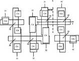
在背景技术中已经提及,静态随机存储器(SRAM)往往具有多个存储单元,且每个存储单元由不同类型的晶体管构成。在此给出典型的六晶体管静态随机存储器(6T-SRAM)单元的构成情况(如图1所示),以便于理解本发明。As mentioned in the background art, a static random access memory (SRAM) often has multiple storage units, and each storage unit is composed of different types of transistors. The composition of a typical six-transistor static random access memory (6T-SRAM) unit (as shown in FIG. 1 ) is given here to facilitate understanding of the present invention.
请参考图1,该6T-SRAM单元包括四个有源区11、21、31和41以及四个栅极12、22、32和42,其形成六个金属氧化物半导体(MOS)晶体管10、20、30、40、50和60,且每个晶体管上均设有金属触点CA以连接其它元件。其中,MOS晶体管10与20为传送门晶体管(PG);MOS晶体管30与40为下拉晶体管(PD);MOS晶体管50与60为上拉晶体管(PU)。下拉晶体管40和上拉晶体管50共用栅极22,且下拉晶体管30和上拉晶体管60共用栅极32。通常,传送门晶体管10和20、下拉晶体管30和40为N沟道金属氧化物半导体(NMOS)晶体管;而上拉晶体管50与60为P沟道金属氧化物半导体(PMOS)晶体管。Please refer to FIG. 1, the 6T-SRAM cell includes four
在现有技术中,为了获得更好的器件性能,往往需对下拉晶体管和上拉晶体管进行阈值电压调整(Vt)注入,而在对下拉晶体管进行Vt注入时,需利用光掩膜遮住上拉晶体管所在区域,完成注入后,去除光掩膜;而后形成新的光掩膜来遮住下拉晶体管所在的区域,完成对上拉晶体管的Vt注入后,去除光掩膜。如此,便需要两次光掩膜的形成与去除过程。本实施例充分考虑到下拉晶体管和上拉晶体管的结构特征,即其具有共用的栅极,从而在对下拉晶体管或上拉晶体管进行栅极刻蚀前注入(pre-gate doping)或后续的阈值电压调整(Vt)注入、晕(halo)注入、轻掺杂漏(LDD)注入、源漏(S/D)注入等时,将会产生注入离子的后续扩散的情况。由于下拉晶体管和上拉晶体管的沟道类型完全相反,注入离子的后续扩散将在彼此的栅极中产生耗尽情况,如此便可影响下拉晶体管或上拉晶体管的阈值电压。故,充分利用离子的后续扩散将可以实现阈值电压的调整。In the prior art, in order to obtain better device performance, it is often necessary to perform threshold voltage adjustment (Vt) injection on the pull-down transistor and the pull-up transistor, and when performing Vt injection on the pull-down transistor, it is necessary to use a photomask to cover the upper After the region where the pull-down transistor is located, the photomask is removed after the injection is completed; then a new photomask is formed to cover the region where the pull-down transistor is located, and the photomask is removed after the Vt implantation of the pull-up transistor is completed. Thus, two photomask formation and removal processes are required. This embodiment fully takes into account the structural characteristics of the pull-down transistor and the pull-up transistor, that is, they have a common gate, so that the pre-gate doping or subsequent threshold value is injected before the gate etching of the pull-down transistor or the pull-up transistor. During voltage adjustment (Vt) implantation, halo (halo) implantation, lightly doped drain (LDD) implantation, source-drain (S/D) implantation, etc., the subsequent diffusion of implanted ions will occur. Since the pull-down and pull-up transistors have opposite channel types, the subsequent diffusion of the implanted ions will create a depletion situation in each other's gate, which can affect the threshold voltage of either the pull-down or pull-up transistor. Therefore, making full use of the subsequent diffusion of ions will enable the adjustment of the threshold voltage.
另外,在对下拉晶体管或上拉晶体管进行栅极刻蚀前注入或后续的Vt注入、晕注入、LDD注入、S/D注入时,下拉晶体管(NMOS)所需的注入离子为N型离子,上拉晶体管(PMOS)所需的注入离子为P型离子;且下拉晶体管的注入离子剂量与能量往往大于上拉晶体管。于是,在这种现有工艺注入条件下作进一步的研究发现,P型注入离子的后续扩散对于下拉晶体管的阈值电压的影响可以忽略不计,而N型注入离子对上拉晶体管阈值电压的影响程度与注入区域至上拉晶体管有源区的距离有关,即改变注入区域与上拉晶体管有源区的距离,将可以调整上拉晶体管的阈值电压。故本实施例利用下拉晶体管的N型离子注入来调整上拉晶体管的阈值电压,从而无需专门针对上拉晶体管进行阈值调整注入,减少了光掩膜的形成与去除过程。In addition, when the pull-down transistor or pull-up transistor is implanted before gate etching or subsequent Vt implantation, halo implantation, LDD implantation, and S/D implantation, the implanted ions required for the pull-down transistor (NMOS) are N-type ions, The implanted ions required by the pull-up transistor (PMOS) are P-type ions; and the implanted ion dose and energy of the pull-down transistor are often greater than those of the pull-up transistor. Therefore, further research under the implantation conditions of this existing process found that the subsequent diffusion of P-type implanted ions has negligible influence on the threshold voltage of the pull-down transistor, while the influence of N-type implanted ions on the threshold voltage of the pull-up transistor is negligible. It is related to the distance from the injection region to the active region of the pull-up transistor, that is, changing the distance between the injection region and the active region of the pull-up transistor can adjust the threshold voltage of the pull-up transistor. Therefore, in this embodiment, the N-type ion implantation of the pull-down transistor is used to adjust the threshold voltage of the pull-up transistor, so that threshold adjustment implantation for the pull-up transistor is not required, and the process of forming and removing the photomask is reduced.
以下将以下拉晶体管40和上拉晶体管50为例,详述如何利用下拉晶体管的N型离子注入来调整上拉晶体管的阈值电压。通常,在进行离子注入前,要利用光掩膜定义离子注入区,同时要设定好离子注入的能量与剂量。而在此能量与剂量确定后,离子的扩散能力也就得以确定,故此时影响扩散入上拉晶体管50栅极的离子数量的主要因素便是离子注入区距离上拉晶体管50的距离。从而,根据上拉晶体管50的阈值电压大小合理设定下拉晶体管40的N型离子注入区距离上拉晶体管50的距离,便可以有效调整上拉晶体管50的阈值电压。The following will take the pull-
基于以上分析,本实施例给出了一种SRAM上拉晶体管阈值电压调整方法,即利用与上拉晶体管共用栅极的下拉晶体管的N型离子注入来调整上拉晶体管的阈值电压,而下拉晶体管的N型离子注入往往包括栅极刻蚀前注入、Vt注入、晕注入、LDD注入或S/D注入等。其详细描述如下:Based on the above analysis, this embodiment provides a method for adjusting the threshold voltage of the SRAM pull-up transistor, that is, using N-type ion implantation of the pull-down transistor that shares the gate with the pull-up transistor to adjust the threshold voltage of the pull-up transistor, and the pull-up transistor N-type ion implantation often includes implantation before gate etching, Vt implantation, halo implantation, LDD implantation or S/D implantation, etc. Its detailed description is as follows:
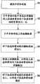
请合并参考图1与图2,该方法包括如下步骤:Please refer to Figure 1 and Figure 2 together, the method includes the following steps:
S1:提供半导体衬底;S1: Provide semiconductor substrate;
S2:于半导体衬底中形成共用栅极的上拉晶体管50与下拉晶体管40的有源区31、41;S2: forming the
S3:于半导体衬底上形成栅极层;S3: forming a gate layer on the semiconductor substrate;
S4:对下拉晶体管40进行栅极刻蚀前注入;S4: Implanting the pull-down
S5:刻蚀上述栅极层,以形成上拉晶体管50与下拉晶体管40的共用栅极22;S5: Etching the above gate layer to form the
S6:对下拉晶体管40进行后续离子注入,以形成下拉晶体管的源漏区。S6: performing subsequent ion implantation on the pull-
进一步参考图3,在进行步骤S4或S6中的离子注入前,包括以下步骤:Further referring to FIG. 3, before performing the ion implantation in step S4 or S6, the following steps are included:
S10:设定相应离子注入区的边缘L与上拉晶体管有源区31的距离,其中该边缘L位于上拉晶体管有源区31与下拉晶体管有源区41之间;S10: setting the distance between the edge L of the corresponding ion implantation region and the
S20:利用光掩膜为下拉晶体管40定义具有边缘L的离子注入区。S20: Define an ion implantation region with an edge L for the pull-
其中上述步骤S4与S6中的注入离子为N型离子。另外,后续离子注入包括阈值电压调整注入、晕注入、轻掺杂漏注入或源漏注入。且通过改变离子注入区的边缘L与上拉晶体管有源区31的距离S可实现不同程度的上拉晶体管阈值电压调整。例如,减少距离S,扩散到上拉晶体管有源区31的N型离子就变多,于是可提高上拉晶体管的阈值电压;相反的,增加距离S可降低上拉晶体管的阈值电压;当距离S增加到一定程度时,扩散到上拉晶体管有源区31的N型离子可忽略,其对上拉晶体管的阈值电压的影响变可以忽略。故在以上方法中可以利用栅极刻蚀前注入、Vt注入、晕注入、LDD注入与S/D注入中的一种注入来实现上拉晶体管阈值电压调整,也可以利用其中几种的组合来实现。Wherein the implanted ions in the above steps S4 and S6 are N-type ions. In addition, the subsequent ion implantation includes threshold voltage adjustment implantation, halo implantation, lightly doped drain implantation or source-drain implantation. And by changing the distance S between the edge L of the ion implantation region and the
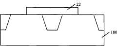
为了更好的理解以上过程,图4至图8通过图1中下拉晶体管40和上拉晶体管50所在区域的I-I方向的截面示意图给出了以上方法于SRAM制造过程中的一种实现过程。In order to better understand the above process, FIG. 4 to FIG. 8 show an implementation process of the above method in the SRAM manufacturing process through the schematic cross-sectional diagrams in the I-I direction of the region where the pull-
如图4,首先,提供半导体衬底100;而后在其中形成多个隔离结构101,从而于两相邻的隔离结构之间定义出有源区;对于上拉晶体管50所在的区域利用N型离子进行阱注入,形成上拉晶体管有源区31;对于下拉晶体管40利用P型离子进行阱注入,形成下拉晶体管有源区41。As shown in Figure 4, at first, a
接着,如图5所示,在半导体衬底100上形成栅极层200,而该栅极层200往往包括栅氧层和栅层,其为本领域技术人员所熟知,故在此不再详述。Next, as shown in FIG. 5 , a
而后,如图6,对所述下拉晶体管40进行栅极刻蚀前注入;以实现下拉晶体管40的栅极电阻的调整,而其注入离子为N型离子,在此步骤中,若合理调整栅极刻蚀前注入区D1的边缘L1与上拉晶体管50有源区31的距离S1,便可以利用其注入离子的后续扩散来调整上拉晶体管50的阈值电压。具体包括:设定栅极刻蚀前注入区D1边缘L1与上拉晶体管有源区31的距离S1,其中该边缘L1位于上拉晶体管有源区31与下拉晶体管有源区41之间;利用光掩膜300为下拉晶体管定义具有该边缘L1的栅极刻蚀前注入区D1;对所述下拉晶体管进行栅极刻蚀前注入。当然也可以将此距离S1设置的足够大,使得此过程中注入的N型离子扩散入有源区31的数量可以忽略,从而只利用后续的N型离子注入来实现调整。Then, as shown in Figure 6, the pull-
如图7,进行栅极层200的刻蚀,以形成所述上拉晶体管50与下拉晶体管40的共用栅极22。As shown in FIG. 7 , the
如图8,对下拉晶体管40进行后续离子注入,其包括Vt注入、晕注入、LDD注入或S/D注入等,以形成下拉晶体管的源漏区500。其注入过程同栅极刻蚀前注入一样,可以通过设置后续离子注入区D2边缘L2与上拉晶体管有源区31的距离S2来决定是否利用其进行上拉晶体管阈值电压调整。如果利用,则包括:设定后续离子注入区D2边缘L2与上拉晶体管有源区31的距离S2,其中该边缘L2位于上拉晶体管有源区31与下拉晶体管有源区41之间;利用光掩膜400为下拉晶体管定义具有边缘L2的后续离子注入区D2;对下拉晶体管进行后续离子注入。以上设定方法适用于Vt注入、晕注入、LDD注入及S/D注入。如果仅利用栅极刻蚀前注入完成上拉晶体管阈值电压调整,则可将距离S2设置的足够大,使得此过程中注入的N型离子扩散入有源区31的数量可以忽略。另外,在此过程中,需于栅极22上形成阻挡层以保护栅极,其为本领域技术人员所熟知,在此不再赘述,故图中也未示出。As shown in FIG. 8 , subsequent ion implantation is performed on the pull-
最后,栅极刻蚀前注入或后续离子注入中注入的离子将进行后续扩散,而实现上拉晶体管的阈值电压调整。Finally, the ions implanted before the gate etching or implanted in the subsequent ion implantation will undergo subsequent diffusion, so as to realize the adjustment of the threshold voltage of the pull-up transistor.
可见,采用以上方法不仅可以避免专门针对上拉晶体管50的Vt调整注入,而减少光掩膜的形成与去除步骤,还可以灵活选择下拉晶体管40的N型离子注入过程来实现上拉晶体管50的阈值电压调整,提高了阈值电压调整的灵活性。It can be seen that using the above method can not only avoid the Vt adjustment implantation specifically for the pull-up
以上是以上拉晶体管50与下拉晶体管40为例进行描述的,而利用下拉晶体管30的N型离子注入调整上拉晶体管60的阈值电压的情况与之类似,在此不再赘述。The pull-up
Claims (4)
Translated fromChinesePriority Applications (1)
| Application Number | Priority Date | Filing Date | Title |
|---|---|---|---|
| CN2008100415697ACN101651121B (en) | 2008-08-11 | 2008-08-11 | Method for adjusting voltage threshold of pull up transistor of static random access memory |
Applications Claiming Priority (1)
| Application Number | Priority Date | Filing Date | Title |
|---|---|---|---|
| CN2008100415697ACN101651121B (en) | 2008-08-11 | 2008-08-11 | Method for adjusting voltage threshold of pull up transistor of static random access memory |
Publications (2)
| Publication Number | Publication Date |
|---|---|
| CN101651121A CN101651121A (en) | 2010-02-17 |
| CN101651121Btrue CN101651121B (en) | 2011-06-15 |
Family
ID=41673310
Family Applications (1)
| Application Number | Title | Priority Date | Filing Date |
|---|---|---|---|
| CN2008100415697AActiveCN101651121B (en) | 2008-08-11 | 2008-08-11 | Method for adjusting voltage threshold of pull up transistor of static random access memory |
Country Status (1)
| Country | Link |
|---|---|
| CN (1) | CN101651121B (en) |
Families Citing this family (4)
| Publication number | Priority date | Publication date | Assignee | Title |
|---|---|---|---|---|
| US8482990B2 (en)* | 2011-02-11 | 2013-07-09 | Taiwan Semiconductor Manufacturing Company, Ltd. | Memory edge cell |
| CN107919327B (en)* | 2016-10-10 | 2020-09-08 | 中芯国际集成电路制造(上海)有限公司 | Semiconductor structure and forming method thereof |
| US10964705B2 (en)* | 2018-09-10 | 2021-03-30 | Semiconductor Components Industries, Llc | Method of forming a semiconductor device |
| CN112038295B (en)* | 2020-11-04 | 2021-02-09 | 晶芯成(北京)科技有限公司 | Semiconductor device and manufacturing method thereof |
Citations (3)
| Publication number | Priority date | Publication date | Assignee | Title |
|---|---|---|---|---|
| US5376577A (en)* | 1994-06-30 | 1994-12-27 | Micron Semiconductor, Inc. | Method of forming a low resistive current path between a buried contact and a diffusion region |
| JPH11265944A (en) | 1998-03-17 | 1999-09-28 | Sanyo Electric Co Ltd | Static semiconductor memory device and method of manufacturing the same |
| CN1901203A (en)* | 2005-07-21 | 2007-01-24 | 台湾积体电路制造股份有限公司 | Semiconductor device and method of forming a semiconductor structure |
- 2008
- 2008-08-11CNCN2008100415697Apatent/CN101651121B/enactiveActive
Patent Citations (3)
| Publication number | Priority date | Publication date | Assignee | Title |
|---|---|---|---|---|
| US5376577A (en)* | 1994-06-30 | 1994-12-27 | Micron Semiconductor, Inc. | Method of forming a low resistive current path between a buried contact and a diffusion region |
| JPH11265944A (en) | 1998-03-17 | 1999-09-28 | Sanyo Electric Co Ltd | Static semiconductor memory device and method of manufacturing the same |
| CN1901203A (en)* | 2005-07-21 | 2007-01-24 | 台湾积体电路制造股份有限公司 | Semiconductor device and method of forming a semiconductor structure |
Also Published As
| Publication number | Publication date |
|---|---|
| CN101651121A (en) | 2010-02-17 |
Similar Documents
| Publication | Publication Date | Title |
|---|---|---|
| US7750416B2 (en) | Modifying work function in PMOS devices by counter-doping | |
| KR960009994B1 (en) | Semiconductor memory device and manufacturing method thereof | |
| US20080283922A1 (en) | Semiconductor device and manufacturing method thereof | |
| CN101651121B (en) | Method for adjusting voltage threshold of pull up transistor of static random access memory | |
| US5986314A (en) | Depletion mode MOS capacitor with patterned Vt implants | |
| US6268250B1 (en) | Efficient fabrication process for dual well type structures | |
| CN112635403B (en) | Preparation method of static random access memory | |
| KR100212173B1 (en) | Manufacturing method of semiconductor device | |
| US7429512B2 (en) | Method for fabricating flash memory device | |
| US7691700B2 (en) | Multi-stage implant to improve device characteristics | |
| JP2001185627A (en) | Semiconductor device and manufacturing method thereof | |
| US20240266173A1 (en) | Method for manufacturing transistor device, and transistor device | |
| KR100387258B1 (en) | Method of manufacturing a transistor in a semiconductor device | |
| US6380594B1 (en) | Semiconductor device | |
| CN111092120A (en) | Field effect transistor device and method of making the same | |
| CN112103189B (en) | Semiconductor device and method for manufacturing the same | |
| KR100308653B1 (en) | Method of forming BILLI well of semiconductor device | |
| US7588991B2 (en) | Method for fabricating embedded static random access memory | |
| KR20040102417A (en) | Pmos elements and manufacture method thereof | |
| US20080090359A1 (en) | Semiconductor device having a p-mos transistor with source-drain extension counter-doping | |
| KR100358571B1 (en) | Manufacturing method of semiconductor device | |
| JPH0778984A (en) | Semiconductor device and manufacturing method thereof | |
| KR100680488B1 (en) | Manufacturing Method of Flash Memory Device | |
| KR20000000625A (en) | Method for manufacturing semiconductor device | |
| KR20010060718A (en) | Method of fabricating cmos transistor for protecting interdiffusion between gate electrodes of that |
Legal Events
| Date | Code | Title | Description |
|---|---|---|---|
| C06 | Publication | ||
| PB01 | Publication | ||
| C10 | Entry into substantive examination | ||
| SE01 | Entry into force of request for substantive examination | ||
| C14 | Grant of patent or utility model | ||
| GR01 | Patent grant |