Movatterモバイル変換


[0]ホーム

URL:


CN101644847B - Liquid-crystal display device and method of manufacturing same - Google Patents

Liquid-crystal display device and method of manufacturing same
Download PDF

Info

Publication number
CN101644847B
CN101644847BCN2009101611406ACN200910161140ACN101644847BCN 101644847 BCN101644847 BCN 101644847BCN 2009101611406 ACN2009101611406 ACN 2009101611406ACN 200910161140 ACN200910161140 ACN 200910161140ACN 101644847 BCN101644847 BCN 101644847B
Authority
CN
China
Prior art keywords
liquid crystal
substrate
layer
crystal display
display device
Prior art date
Legal status (The legal status is an assumption and is not a legal conclusion. Google has not performed a legal analysis and makes no representation as to the accuracy of the status listed.)
Active
Application number
CN2009101611406A
Other languages
Chinese (zh)
Other versions
CN101644847A (en
Inventor
小系健夫
永泽耕一
林宗治
小坂英宽
Current Assignee (The listed assignees may be inaccurate. Google has not performed a legal analysis and makes no representation or warranty as to the accuracy of the list.)
Japan Display Inc
Original Assignee
Sony Corp
Priority date (The priority date is an assumption and is not a legal conclusion. Google has not performed a legal analysis and makes no representation as to the accuracy of the date listed.)
Filing date
Publication date
Application filed by Sony CorpfiledCriticalSony Corp
Publication of CN101644847ApublicationCriticalpatent/CN101644847A/en
Application grantedgrantedCritical
Publication of CN101644847BpublicationCriticalpatent/CN101644847B/en
Activelegal-statusCriticalCurrent
Anticipated expirationlegal-statusCritical

Links

Images

Classifications

Landscapes

Abstract

The invention relates to a liquid-crystal display device and a method of manufacturing the same. The liquid-crystal display device includes a first substrate; a second substrate formed so as to oppose the first substrate; a liquid-crystal layer with a predetermined thickness, the liquid-crystal layer being formed between the first substrate and the second substrate; a planarization film for planarizing the surface of the liquid-crystal layer, the planarization film being formed on the surface of at least one of the first substrate and the second substrate, the surface facing the liquid-crystal layer; and projecting parts that are integrally formed with the planarization film.

Description

Translated fromChinese
液晶显示装置及其制造方法Liquid crystal display device and manufacturing method thereof

技术领域technical field

本发明涉及液晶显示装置和制造液晶显示装置的方法。The present invention relates to a liquid crystal display device and a method of manufacturing a liquid crystal display device.

背景技术Background technique

液晶显示装置具有诸如外形小、重量轻和功耗低之类的优点。因此,液晶显示装置常用于诸如移动电话或数码相机之类的移动电子设备中。液晶显示装置包括具有封在一对基板之间的液晶层的液晶面板,使得从设在液晶面板的背面上的平面光源(例如背光)发出的光由液晶面板所调制。然后,经调制的光使得图像能够显示在液晶面板的正面上。Liquid crystal display devices have advantages such as small size, light weight, and low power consumption. Therefore, liquid crystal display devices are often used in mobile electronic devices such as mobile phones or digital cameras. A liquid crystal display device includes a liquid crystal panel having a liquid crystal layer sealed between a pair of substrates such that light emitted from a planar light source (eg, backlight) provided on the back of the liquid crystal panel is modulated by the liquid crystal panel. The modulated light then enables an image to be displayed on the front side of the liquid crystal panel.

近年来,已经使用包括触摸板的液晶显示装置,其中通过该触摸板,用户可通过直接触摸液晶显示装置的屏幕上所显示的图标来输入用户指定的内容。In recent years, a liquid crystal display device including a touch panel through which a user can input user-designated content by directly touching an icon displayed on a screen of the liquid crystal display device has been used.

该触摸板设置在液晶显示装置的最上侧,从而可通过利用人的手或者利用物体直接触摸来选择液晶显示装置的屏幕上所显示的指定内容。在触摸板中,检测手或物体与其所接触的位置,并且通过将接触位置处所指定的内容用作输入信号,来驱动液晶显示装置。在包括触摸板的液晶显示装置用于计算机等、用于诸如键盘或鼠标之类的输入装置或者用于诸如移动电话之类的移动产品的情况下,包括触摸板的液晶显示装置不必单独具有输入装置。结果,在越来越多地使用触摸板。The touch panel is provided at the uppermost side of the liquid crystal display device so that specified content displayed on the screen of the liquid crystal display device can be selected by directly touching with a human hand or with an object. In the touch panel, a position where a hand or an object is in contact with is detected, and a liquid crystal display device is driven by using what is specified at the contact position as an input signal. In the case where a liquid crystal display device including a touch panel is used for a computer or the like, for an input device such as a keyboard or a mouse, or for a mobile product such as a mobile phone, the liquid crystal display device including a touch panel does not necessarily have an input device. As a result, touchpads are being used more and more.

另一方面,在通过将触摸板布置在液晶显示装置上而包括触摸板的产品中,由于装置厚度或尺寸的增大并且由于折射面的影响而发生光学特性的降低。此外,存在由于除液晶显示装置之外还需要触摸板的事实所引起的制造成本升高的问题,并且已建议将液晶显示装置和触摸板一体地形成。On the other hand, in a product including a touch panel by arranging it on a liquid crystal display device, degradation of optical characteristics occurs due to an increase in thickness or size of the device and due to the influence of a refractive surface. Furthermore, there is a problem of increased manufacturing cost due to the fact that a touch panel is required in addition to the liquid crystal display device, and it has been proposed to integrally form the liquid crystal display device and the touch panel.

近年来,已提出了具有所谓传感器功能的液晶显示装置,其中液晶显示装置和触摸板一体地形成。在下面描述的日本未审查专利申请公开No.2007-95044中的一种具有传感器功能的液晶显示装置中,描述了一种方法,其中在手或物体接触液晶显示装置的液晶面板时产生的外部压力通过形成液晶面板的一对基板之间的电接触来检测。In recent years, a liquid crystal display device having a so-called sensor function in which the liquid crystal display device and a touch panel are integrally formed has been proposed. In a liquid crystal display device with a sensor function in Japanese Unexamined Patent Application Publication No. 2007-95044 described below, a method is described in which an external The pressure is detected by electrical contact between a pair of substrates forming the liquid crystal panel.

图10示出了现有技术的具有传感器功能的液晶显示装置100的示意构造。现有技术的具有传感器功能的液晶显示装置100配置为包括阵列基板101、与阵列基板101相对(oppose)地设置的对向基板102以及设在阵列基板101与对向基板102之间的液晶层103。FIG. 10 shows a schematic configuration of a conventional liquidcrystal display device 100 with a sensor function. A conventional liquidcrystal display device 100 having a sensor function is configured to include anarray substrate 101, anopposing substrate 102 disposed opposite to thearray substrate 101, and a liquid crystal layer disposed between thearray substrate 101 and theopposing substrate 102. 103.

首先将描述阵列基板101。First, thearray substrate 101 will be described.

阵列基板101配置为具有绝缘基板104和薄膜晶体管(下面称为TFT)107,绝缘基板104由透明矩形平板状的玻璃形成,TFT 107由多个与绝缘基板104上的像素相对应的开关元件形成。然后,在TFT 107上,在用于覆盖TFT 107以便实现平坦化的平坦化膜105上按图案形成(pattern-formed)像素电极106,像素电极106通过平坦化膜105上形成的接触部分118而连接到TFT 107。此外,定向膜108设在像素电极106上。Thearray substrate 101 is configured to have aninsulating substrate 104 and a thin film transistor (hereinafter referred to as TFT) 107, theinsulating substrate 104 is formed of transparent rectangular plate-shaped glass, and the TFT 107 is formed by a plurality of switching elements corresponding to pixels on theinsulating substrate 104 . Then, on theTFT 107, apixel electrode 106 is pattern-formed on theplanarization film 105 for covering theTFT 107 so as to achieve planarization, and thepixel electrode 106 is connected through thecontact portion 118 formed on theplanarization film 105. Connect to TFT 107. In addition, analignment film 108 is provided on thepixel electrode 106 .

接下来将给出对对向基板102的描述。Next, a description will be given of thecounter substrate 102 .

对向基板102包括透明绝缘基板109(例如玻璃或者聚碳酸酯(PC))、在绝缘基板109的一个主面上形成的滤色层110和在滤色层110上形成的平坦化膜111。此外,突起状的传感器调整层115和在包括传感器调整层115的整个表面上形成的公共电极112设置在平坦化膜111上。此外,为了保持液晶层103的厚度而形成的定距器层(spacer layer)114和在整个表面上除定距器层114之外的地方形成的定向膜113设置在公共电极112的预定位置处。Thecounter substrate 102 includes atransparent insulating substrate 109 such as glass or polycarbonate (PC), acolor filter layer 110 formed on one main surface of theinsulating substrate 109 , and aplanarization film 111 formed on thecolor filter layer 110 . In addition, a protrusion-shapedsensor adjustment layer 115 and acommon electrode 112 formed on the entire surface including thesensor adjustment layer 115 are provided on theplanarization film 111 . In addition, aspacer layer 114 formed to maintain the thickness of theliquid crystal layer 103 and analignment film 113 formed on the entire surface except for thespacer layer 114 are provided at predetermined positions of thecommon electrode 112 .

滤色层110由树脂膜形成,其中包含具有红(R)、绿(G)和蓝(B)三基色的染料或颜料。Thecolor filter layer 110 is formed of a resin film containing dyes or pigments having three primary colors of red (R), green (G) and blue (B).

平坦化膜111用于使滤色层110的表面平坦化,并且由发光材料形成。Theplanarization film 111 is used to planarize the surface of thecolor filter layer 110, and is formed of a light emitting material.

传感器调整层115以突起状的形式形成于平坦化膜111上的预定位置处,并且形成为具有小于单元厚度(液晶层103的厚度)的值。公共电极112形成于包含该传感器调整层115的整个表面上。在现有技术的示例中,由在该传感器调整层115上所形成的公共电极112形成传感器电极116。Thesensor adjustment layer 115 is formed in a protrusion shape at a predetermined position on theplanarizing film 111 and formed to have a value smaller than the cell thickness (thickness of the liquid crystal layer 103 ). Thecommon electrode 112 is formed on the entire surface including thesensor adjustment layer 115 . In the related art example, thesensor electrode 116 is formed by thecommon electrode 112 formed on thesensor adjustment layer 115 .

此外,定距器层114以隔开的方式等间隔地形成在公共电极112上,并且按单元厚度的预定高度以柱状形成。这些定距器层114使得能够保持阵列基板101与对向基板102之间的单元厚度。In addition, thespacer layer 114 is formed at equal intervals on thecommon electrode 112 in a spaced manner, and is formed in a columnar shape at a predetermined height of a cell thickness. Thesespacer layers 114 enable maintaining the cell thickness between thearray substrate 101 and thecounter substrate 102 .

对向基板102和阵列基板101形成为保持预定的单元厚度,并且以各定向膜108和113向内面对的方式彼此相对。该单元厚度通过定距器层114的高度而在表面上保持恒定,并且通过封在该单元厚度内的预定液晶材料,形成了液晶层103。Theopposite substrate 102 and thearray substrate 101 are formed to maintain a predetermined cell thickness, and are opposed to each other with therespective alignment films 108 and 113 facing inward. The cell thickness is kept constant over the surface by the height of thespacer layer 114, and theliquid crystal layer 103 is formed by a predetermined liquid crystal material enclosed within the cell thickness.

在具有以上构造的液晶显示装置100中,传感器电极116和在与该传感器电极116相对的位置处的像素电极106构成触摸传感器。In the liquidcrystal display device 100 having the above configuration, thesensor electrode 116 and thepixel electrode 106 at a position opposed to thesensor electrode 116 constitute a touch sensor.

在图10所示的液晶显示装置100中,通过利用诸如手或手指之类的触摸体117按压对向基板102而施加压力。于是,使得传感器电极116经由定向膜108和113而接触与传感器电极116相对的阵列基板101的像素电极106。通过检测传感器电极116与像素电极106之间的接触,可以检测触摸体所触摸的位置。In the liquidcrystal display device 100 shown in FIG. 10 , pressure is applied by pressing thecounter substrate 102 with atouch body 117 such as a hand or a finger. Thus, thesensor electrode 116 is brought into contact with thepixel electrode 106 of thearray substrate 101 opposite to thesensor electrode 116 via thealignment films 108 and 113 . By detecting the contact between thesensor electrode 116 and thepixel electrode 106, the position touched by the touch body can be detected.

在这种现有技术的具有传感器功能的液晶显示装置100中,传感器电极116和像素电极106的电连接使得检测到触摸体117所触摸的位置。因此,这两个电极之间的距离越小,对施加小外部压力的触摸位置的检测越容易。因此,对于现有技术的具有传感器功能的液晶显示装置100,如图10所示,可以看到许多示例,其中在平坦化膜111上形成以突起状形式形成的传感器调整层115,并且调整传感器电极116的高度。In this conventional liquidcrystal display device 100 with a sensor function, the electrical connection between thesensor electrode 116 and thepixel electrode 106 enables detection of the position touched by thetouch body 117 . Therefore, the smaller the distance between these two electrodes, the easier the detection of the touch position where a small external pressure is applied. Therefore, for the related art liquidcrystal display device 100 having a sensor function, as shown in FIG. The height of theelectrode 116.

然而,对于这种突起状的传感器调整层115与作为传感器调整层115下的层的平坦化膜111之间的接合面积,确保接合强度是困难的,这是因为接合区域通常是直径在数微米量级上的非常小的区域。However, it is difficult to secure the bonding strength for the bonding area between such a protrudingsensor adjustment layer 115 and theplanarizing film 111 as a layer below thesensor adjustment layer 115 because the bonding area is usually several microns in diameter. A very small area of magnitude.

此外,柱状的定距器层114通常形成在公共电极113上。一般而言,公共电极113与定距器层114之间的接触程度较弱,并且定距器层114容易剥离。In addition, acolumnar spacer layer 114 is generally formed on thecommon electrode 113 . Generally speaking, the contact degree between thecommon electrode 113 and thespacer layer 114 is weak, and thespacer layer 114 is easy to peel off.

发明内容Contents of the invention

如上所述,在从液晶显示装置100的显示屏上直接施加外部压力以检测外部压力所施加的位置的构造中,由于液晶显示装置100直接接收外部压力,有必要使得液晶显示装置100能够抗外部压力。然而,如上所述,在现有技术的液晶显示装置100中,对向基板102上所形成的结构体(例如定距器层114、传感器调整层115等)容易剥离。特别地,在执行要求物理强度的测试(例如按键测试(keying test)、滑动测试等)的情况下,存在以下情况:在作为触摸传感器而工作的传感器电极116之下的层中形成的突起状的传感器调整层115从对向基板102的表面剥离。于是,在所显示的图像中出现亮点或暗点,并且出现显示缺陷和传感器灵敏度缺陷。此外,由于定距器层114的剥离而发生的间隙变更和由于结构体的剥离而在单元内发生的异物都成为问题。As described above, in the configuration in which external pressure is directly applied from the display screen of the liquidcrystal display device 100 to detect the position to which the external pressure is applied, since the liquidcrystal display device 100 directly receives the external pressure, it is necessary to make the liquidcrystal display device 100 resistant to external pressure. pressure. However, as mentioned above, in the conventional liquidcrystal display device 100 , the structures formed on the counter substrate 102 (for example, thespacer layer 114 , thesensor adjustment layer 115 , etc.) are easily peeled off. In particular, in the case of performing a test requiring physical strength (such as a keying test, a slide test, etc.), there are cases where protrusions formed in the layer below thesensor electrodes 116 functioning as a touch sensor Thesensor adjustment layer 115 is peeled off from the surface of thecounter substrate 102 . Then, bright or dark spots appear in the displayed image, and display defects and sensor sensitivity defects occur. In addition, changes in the gap due to the peeling of thespacer layer 114 and foreign matter generated in the cell due to the peeling of the structure are problems.

另外,近年来,在以下环境中的使用增加:其中,由于使用FF(膜-膜)触摸板所引起的液晶显示装置的小外形和轻重量,对液晶显示装置的显示屏的压力和冲击比以前所施加的更大。此外,目前,当使用液晶显示装置的电子设备扩展时,需要可以耐受对显示屏的压力和冲击的液晶显示装置。In addition, in recent years, use has increased in environments where pressure and impact on the display screen of a liquid crystal display device are greater than What was previously imposed is greater. In addition, at present, when electronic equipment using liquid crystal display devices expands, liquid crystal display devices that can withstand pressure and impact to a display screen are required.

希望提供一种具有抗外部压力的单元结构的液晶显示装置和制造该液晶显示装置的方法。It is desirable to provide a liquid crystal display device having a cell structure resistant to external pressure and a method of manufacturing the liquid crystal display device.

根据本发明的一个实施例,提供了一种液晶显示装置,包括:第一基板;与第一基板相对地形成的第二基板;具有预定厚度的液晶层,该液晶层形成在第一基板和第二基板之间;用于使液晶层的表面平坦化的平坦化膜,该平坦化膜形成在第一基板和第二基板中的至少一者的面对液晶层的表面上;以及与平坦化膜一体地形成的突起部分。According to one embodiment of the present invention, a liquid crystal display device is provided, comprising: a first substrate; a second substrate formed opposite to the first substrate; a liquid crystal layer having a predetermined thickness formed on the first substrate and the liquid crystal layer between the second substrates; a planarizing film for planarizing the surface of the liquid crystal layer, the planarizing film being formed on a surface of at least one of the first substrate and the second substrate facing the liquid crystal layer; The protruding part formed integrally with the chemical film.

在根据本发明实施例的液晶显示装置中,突起部分与平坦化膜一体地形成。结果,突起部分与第一基板或第二基板之间的接合表面增大,并且突起部分从第一基板或第二基板的剥离强度增大。In the liquid crystal display device according to the embodiment of the present invention, the protruding portion is integrally formed with the planarizing film. As a result, the bonding surface between the protruding portion and the first substrate or the second substrate increases, and the peel strength of the protruding portion from the first substrate or the second substrate increases.

根据本发明的另一实施例,提供了一种制造液晶显示装置的方法,该方法包括以下步骤:制备第一基板,其中该第一基板上形成多个薄膜晶体管;制备与第一基板相层压的第二基板,其中具有预定厚度的液晶层插入第一基板与第二基板之间;以及在第一基板和第二基板中的至少一者的面对液晶层的表面上形成平坦化膜,并且以与平坦化膜一体地形成的形式形成突起状的突起部分。According to another embodiment of the present invention, a method for manufacturing a liquid crystal display device is provided, the method including the following steps: preparing a first substrate, wherein a plurality of thin film transistors are formed on the first substrate; a pressed second substrate, wherein a liquid crystal layer having a predetermined thickness is interposed between the first substrate and the second substrate; and a planarization film is formed on a surface facing the liquid crystal layer of at least one of the first substrate and the second substrate , and a protruding protruding portion is formed integrally with the planarizing film.

在根据本发明实施例的制造液晶显示装置的方法中,突起部分与平坦化膜一体地形成。结果,突起部分与第一基板或第二基板之间的接合表面增大,并且突起部分从第一基板或第二基板的剥离强度增大。此外,在本发明的实施例中,由于突起部分与平坦化膜一体地形成,因此突起部分的形成和平坦化膜的形成可同时执行,从而可以减少步骤数。In the method of manufacturing a liquid crystal display device according to an embodiment of the present invention, the protruding portion is integrally formed with the planarizing film. As a result, the bonding surface between the protruding portion and the first substrate or the second substrate increases, and the peel strength of the protruding portion from the first substrate or the second substrate increases. Furthermore, in the embodiments of the present invention, since the protruding portion is integrally formed with the planarizing film, the formation of the protruding portion and the forming of the planarizing film can be performed simultaneously, so that the number of steps can be reduced.

根据本发明的实施例,可以获得一种抗外部压力并且具有高可靠性的液晶显示装置。According to the embodiments of the present invention, a liquid crystal display device resistant to external pressure and having high reliability can be obtained.

附图说明Description of drawings

图1是根据本发明第一实施例的液晶显示装置的示意截面图;图2A、2B、2C和2D是根据本发明第一实施例的液晶显示装置的制造步骤图;图3示出本发明的液晶显示装置和现有技术的液晶显示装置中的按键测试结果;图4是根据本发明第二实施例的液晶显示装置的示意截面图;图5是根据本发明第三实施例的液晶显示装置的示意截面图;图6是根据本发明第四实施例的液晶显示装置的示意截面图;图7是根据本发明第五实施例的液晶显示装置的示意截面图;图8是根据本发明第六实施例的液晶显示装置的示意截面图;图9是根据本发明第七实施例的液晶显示装置的示意截面图;以及图10是现有技术的液晶显示装置的示意截面图。Fig. 1 is a schematic sectional view of a liquid crystal display device according to a first embodiment of the present invention; Fig. 2A, 2B, 2C and 2D are manufacturing step diagrams of a liquid crystal display device according to a first embodiment of the present invention; Fig. 3 shows the present invention The key test results in the liquid crystal display device of the present invention and the liquid crystal display device of prior art; Fig. 4 is the schematic sectional view of the liquid crystal display device according to the second embodiment of the present invention; Fig. 5 is the liquid crystal display device according to the third embodiment of the present invention A schematic sectional view of the device; FIG. 6 is a schematic sectional view of a liquid crystal display device according to a fourth embodiment of the present invention; FIG. 7 is a schematic sectional view of a liquid crystal display device according to a fifth embodiment of the present invention; FIG. 8 is a schematic sectional view according to thepresent invention 9 is a schematic cross-sectional view of a liquid crystal display device according to a seventh embodiment of the present invention; and FIG. 10 is a schematic cross-sectional view of a prior art liquid crystal display device.

具体实施方式Detailed ways

下面将参考附图来描述本发明的实施例。Embodiments of the present invention will be described below with reference to the drawings.

第一实施例first embodiment

图1示出了根据本发明第一实施例的液晶显示装置1的示意构造。根据本示例性实施例的液晶显示装置1是具有传感器功能的液晶显示装置,该传感器功能能够检测显示屏被触摸的位置。FIG. 1 shows a schematic configuration of a liquidcrystal display device 1 according to a first embodiment of the present invention. The liquidcrystal display device 1 according to the present exemplary embodiment is a liquid crystal display device having a sensor function capable of detecting a position where the display screen is touched.

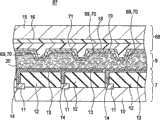
根据本示例性实施例的液晶显示装置1具有阵列基板7和对向基板8,阵列基板7是在一侧上形成有多个薄膜晶体管(下面称为TFT)11的第一基板,对向基板8是与阵列基板7相对地设置的第二基板。然后,液晶显示装置1由阵列基板7、对向基板8和形成在这两个基板之间且具有预定厚度的液晶层9构成。下面,将以该顺序来描述阵列基板7、对向基板8和液晶层9。The liquidcrystal display device 1 according to the present exemplary embodiment has anarray substrate 7 which is a first substrate on which a plurality of thin film transistors (hereinafter referred to as TFTs) 11 are formed on one side, and an opposingsubstrate 8 . 8 is a second substrate provided opposite to thearray substrate 7 . Then, the liquidcrystal display device 1 is composed of anarray substrate 7, acounter substrate 8, and aliquid crystal layer 9 formed between these two substrates and having a predetermined thickness. Hereinafter, thearray substrate 7, thecounter substrate 8, and theliquid crystal layer 9 will be described in this order.

阵列基板7配置为包括由透明矩形平板状的玻璃形成的绝缘基板10和形成在绝缘基板10的面对液晶层9的表面上的多个TFT 11。多个TFT11以对应于像素的方式按阵列设置,并且用作开关元件。然后,以覆盖TFT 11的方式在绝缘基板10的整个表面上形成平坦化膜12。该平坦化膜12形成有接触部分14,TFT 11的一部分从每个接触部分14露出。该平坦化膜12形成为使得阵列基板7的面对液晶层9的表面上除了接触部分14之外的部分平坦化。此外,在平坦化膜12上,以对应于相应一个像素的方式按图案形成像素电极13。各像素电极13经由平坦化膜12上所形成的接触部分14而连接到作为开关元件的TFT 11。这些像素电极13形成为透明电极并且例如利用ITO(氧化铟锡)形成。Thearray substrate 7 is configured to include an insulatingsubstrate 10 formed of transparent rectangular flat glass and a plurality ofTFTs 11 formed on a surface of the insulatingsubstrate 10 facing theliquid crystal layer 9. A plurality ofTFTs 11 are arranged in an array corresponding to pixels, and function as switching elements. Then, aplanarizing film 12 is formed on the entire surface of the insulatingsubstrate 10 so as to cover theTFT 11. Theplanarizing film 12 is formed withcontact portions 14 each of which a part of theTFT 11 is exposed. Theplanarizing film 12 is formed to planarize a portion of the surface of thearray substrate 7 facing theliquid crystal layer 9 except for thecontact portion 14 . Further, on theplanarizing film 12 , thepixel electrodes 13 are patterned in such a manner as to correspond to a corresponding one pixel. Eachpixel electrode 13 is connected to aTFT 11 as a switching element via acontact portion 14 formed on theplanarizing film 12. Thesepixel electrodes 13 are formed as transparent electrodes and are formed using ITO (Indium Tin Oxide), for example.

此外,在像素电极13上,在覆盖像素电极13的整个表面上形成定向膜20。Further, on thepixel electrode 13 , analignment film 20 is formed covering the entire surface of thepixel electrode 13 .

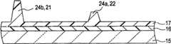
对向基板8由透明绝缘基板15(例如玻璃或者聚碳酸酯(PC))、在绝缘基板15的面对液晶层9的表面上形成的滤色层16以及在滤色层16上形成的平坦化膜17构成。然后,对向基板8具有与平坦化膜17一体地形成的突起部分24a和24b。在本示例性实施例中,突起部分24a和24b分别构成传感器调整层22和定距器层21。在整个表面上除该定距器层21之外的地方形成公共电极18,并且在公共电极18上形成定向膜19。Theopposite substrate 8 is made of a transparent insulating substrate 15 (such as glass or polycarbonate (PC)), acolor filter layer 16 formed on the surface of the insulatingsubstrate 15 facing theliquid crystal layer 9, and a flat surface formed on thecolor filter layer 16.Chemical film 17 constitutes. Then, thecounter substrate 8 has the protrudingportions 24 a and 24 b integrally formed with theplanarization film 17 . In the present exemplary embodiment, the protrudingportions 24a and 24b constitute thesensor adjustment layer 22 and thespacer layer 21, respectively. Thecommon electrode 18 is formed on the entire surface except for thespacer layer 21 , and thealignment film 19 is formed on thecommon electrode 18 .

滤色层16由树脂膜形成,其中包含具有红(R)、绿(G)和蓝(B)三基色的染料或颜料。Thecolor filter layer 16 is formed of a resin film containing dyes or pigments having three primary colors of red (R), green (G), and blue (B).

平坦化膜17形成为使得对向基板8的面对液晶层9的表面平坦化。特别地,使得除与平坦化膜17一体地形成的突起部分24a和24b之外的表面平坦。分别有突起部分24a和24b形成的定距器层21和传感器调整层22优选地形成在如下位置:在该位置处,它们由液晶显示装置1中的遮光膜(未示出)等所遮光。定距器层21形成为使得液晶层9的厚度(即,单元厚度)得以保持以便在在平面内恒定,并且形成为一高度,其中单元厚度在该高度时达到预定厚度。Theplanarizing film 17 is formed to planarize the surface of thecounter substrate 8 facing theliquid crystal layer 9 . In particular, the surface other than the protrudingportions 24 a and 24 b integrally formed with theplanarizing film 17 is made flat. Thespacer layer 21 and thesensor adjustment layer 22 respectively formed with the protrudingportions 24a and 24b are preferably formed at positions where they are shielded from light by a light shielding film (not shown) or the like in the liquidcrystal display device 1 . Thespacer layer 21 is formed so that the thickness of the liquid crystal layer 9 (ie, cell thickness) is maintained so as to be constant in a plane, and is formed to a height at which the cell thickness reaches a predetermined thickness.

传感器调整层22形成为低于定距器层21,并且在传感器调整层22上所形成的像素电极18形成为传感器电极25。即,传感器调整层22用于实现在对向基板8的一侧上形成的传感器电极25的高度。Thesensor adjustment layer 22 is formed lower than thespacer layer 21 , and thepixel electrodes 18 formed on thesensor adjustment layer 22 are formed assensor electrodes 25 . That is, thesensor adjustment layer 22 is used to realize the height of thesensor electrodes 25 formed on the side of the opposingsubstrate 8 .

下面将参考图2A至2D来给出对制造具有以上构造的对向基板8的方法的描述。A description will be given below of a method ofmanufacturing counter substrate 8 having the above configuration with reference to FIGS. 2A to 2D .

首先,如图2A所示,在绝缘基板15上形成滤色层16,并且在滤色层16上形成具有预定厚度的感光树脂膜17a。至于感光树脂膜17a的材料,可以使用正或负感光树脂材料。在本示例性实施例中,使用正感光树脂材料。然后,用掩模80对以上述方式形成的感光树脂膜17a内成为上述定距器层21和传感器调整层22的部分遮光,并且将其暴露于光。First, as shown in FIG. 2A , acolor filter layer 16 is formed on an insulatingsubstrate 15 , and aphotosensitive resin film 17 a having a predetermined thickness is formed on thecolor filter layer 16 . As for the material of thephotosensitive resin film 17a, positive or negative photosensitive resin materials can be used. In this exemplary embodiment, a positive photosensitive resin material is used. Then, the portion to be thespacer layer 21 and thesensor adjustment layer 22 in thephotosensitive resin film 17a formed in the above manner is shielded from light with themask 80 and exposed to light.

接下来,如图2B所示,利用掩模81仅对感光树脂膜17a内用作传感器调整层22的部分遮光并将其暴露于光。此后,在经过显影步骤之后,如图2C所示,形成平坦化膜17以及与平坦化膜17一体地形成且分别用作传感器调整层22和定距器层21的突起部分24a和24b。如上所述,通过对感光树脂膜17a曝光两次,可以形成具有不同高度的突起部分24a和24b,并且可以将传感器调整层22和定距器层21形成为达到所需的各自高度。Next, as shown in FIG. 2B , only a portion serving as thesensor adjustment layer 22 within thephotosensitive resin film 17 a is shielded from light using amask 81 and exposed to light. Thereafter, after passing through the developing step, as shown in FIG. 2C , aplanarization film 17 andprotrusions 24 a and 24 b integrally formed with theplanarization film 17 and serving as thesensor adjustment layer 22 and thespacer layer 21 , respectively, are formed. As described above, by exposing thephotosensitive resin film 17a twice, the protrudingportions 24a and 24b having different heights can be formed, and thesensor adjustment layer 22 and thespacer layer 21 can be formed to desired respective heights.

一般而言,存在对易于控制到以下程度的要求:影响传感器灵敏度的突起部分24a略低于用作定距器层21的突起部分24b,并且其高度约为0.2至0.5μm。根据本示例性实施例,可以控制通过仅调整曝光量所形成的突起部分24a和24b的高度,并且可以高精度地形成突起部分24a和24b。In general, there is a demand for easy control to the extent that the protrudingportion 24a affecting sensor sensitivity is slightly lower than the protrudingportion 24b serving as thespacer layer 21 and its height is about 0.2 to 0.5 μm. According to the present exemplary embodiment, the heights of the protrudingportions 24a and 24b formed by only adjusting the exposure amount can be controlled, and the protrudingportions 24a and 24b can be formed with high precision.

此后,如图2D所示,在整个表面上除成为定距器层21的部分之外的地方形成公共电极18和定向膜19。公共电极18形成为透明电极;例如可以使用ITO。Thereafter, as shown in FIG. 2D , thecommon electrode 18 and thealignment film 19 are formed on the entire surface except for the portion to be thespacer layer 21 . Thecommon electrode 18 is formed as a transparent electrode; for example, ITO can be used.

通过以上步骤,完成了对向基板8,其中一体地形成了突起部分24a和24b以及平坦化膜17。在本示例性实施例的制造方法中,描述了如下示例:其中在经历两次曝光步骤之后,形成具有不同高度的突起部分24a和24b。或者,在曝光步骤中,通过使用半色调掩模(halftone mask)来控制对所投射的光的曝光量,也可以形成具有不同高度的突起部分24a和24b。在使用半色调掩模的情况下,可以减少掩模数,并且可以缩短制造时间。Through the above steps, thecounter substrate 8 in which the protrudingportions 24 a and 24 b and theplanarizing film 17 are integrally formed is completed. In the manufacturing method of the present exemplary embodiment, an example is described in which the protrudingportions 24 a and 24 b having different heights are formed after undergoing two exposure steps. Alternatively, in the exposure step, by using a halftone mask to control the exposure amount to the projected light, it is also possible to form the protrudingportions 24a and 24b having different heights. In the case of using a halftone mask, the number of masks can be reduced, and the manufacturing time can be shortened.

在本示例性实施例的制造液晶显示装置1的方法中,由于平坦化膜17以及突起部分24a和24b一体地形成,因此与现有技术不同,不必在单独的步骤中形成突起部分24a和24b以及平坦化膜17,从而减少了步骤数。In the method of manufacturing the liquidcrystal display device 1 of this exemplary embodiment, since the flatteningfilm 17 and the protrudingparts 24a and 24b are integrally formed, it is not necessary to form the protrudingparts 24a and 24b in a separate step unlike the related art and theplanarization film 17, thereby reducing the number of steps.

上述阵列基板7和对向基板8在以下状态用密封剂(未示出)层压:与定距器层21的高度相对应的量的单元厚度得以保持,使得它们各自的定向膜20和19向内面对。Thearray substrate 7 and thecounter substrate 8 described above are laminated with a sealant (not shown) in a state where the cell thickness of an amount corresponding to the height of thespacer layer 21 is maintained so that theirrespective alignment films 20 and 19 Face inward.

液晶层9以如下方式形成:在布置为使得它们各自的定向膜20和19彼此面对的阵列基板7与对向基板8之间,密封液晶。阵列基板7与对向基板8之间的距离(即,单元厚度)由定距器层21的高度指定,并且单元厚度达到液晶层9的厚度。在本示例性实施例的液晶显示装置1中,通过对阵列基板7一侧上的像素电极13进行图案化,未引起短路。或者,对向电极9一侧上的公共电极18可按图案形成。Theliquid crystal layer 9 is formed in such a manner that the liquid crystal is sealed between thearray substrate 7 and thecounter substrate 8 arranged such that theirrespective alignment films 20 and 19 face each other. The distance between thearray substrate 7 and the counter substrate 8 (ie, the cell thickness) is specified by the height of thespacer layer 21 , and the cell thickness reaches the thickness of theliquid crystal layer 9 . In the liquidcrystal display device 1 of the present exemplary embodiment, by patterning thepixel electrodes 13 on thearray substrate 7 side, no short circuit is caused. Alternatively, thecommon electrode 18 on thecounter electrode 9 side may be formed in a pattern.

在本示例性实施例的液晶显示装置1中,对向基板8的与液晶层9的表面相反的表面用作显示屏。此外,在本示例性实施例中,在与传感器电极25相对的位置处的像素电极13构成根据本发明一实施例的对向电极。然后,在本示例性实施例的液晶显示装置1中,对向基板8上所形成的传感器电极25和阵列基板7上在与传感器电极25相对的位置处形成的像素电极13(对向电极)构成触摸传感器。In the liquidcrystal display device 1 of the present exemplary embodiment, the surface of thecounter substrate 8 opposite to the surface of theliquid crystal layer 9 functions as a display screen. Furthermore, in the present exemplary embodiment, thepixel electrode 13 at a position opposed to thesensor electrode 25 constitutes a counter electrode according to an embodiment of the present invention. Then, in the liquidcrystal display device 1 of the present exemplary embodiment, thesensor electrodes 25 formed on thecounter substrate 8 and the pixel electrodes 13 (counter electrodes) formed on thearray substrate 7 at positions opposed to thesensor electrodes 25 Constitutes a touch sensor.

触摸传感器用于检测施加到显示屏上的外部压力,并且能够在压力由诸如手或手指之类的触摸体施加到显示屏上时检测触摸位置。The touch sensor is used to detect external pressure applied to the display screen, and is capable of detecting a touch position when pressure is applied to the display screen by a touch body such as a hand or a finger.

在具有以上构造的液晶显示装置1中,通过在公共电极18与像素电极13之间施加电压,改变了液晶层9的液晶的取向状态。然后,从阵列基板7发出的来自光源(未示出)的光由液晶层9所调制,从而使得所需图像显示在显示屏上。In the liquidcrystal display device 1 having the above configuration, by applying a voltage between thecommon electrode 18 and thepixel electrode 13, the alignment state of the liquid crystal of theliquid crystal layer 9 is changed. Then, light from a light source (not shown) emitted from thearray substrate 7 is modulated by theliquid crystal layer 9, so that desired images are displayed on the display screen.

此外,在本示例性实施例的液晶显示装置1中,例如在由诸如手或手指之类的触摸体从对向基板8外部施加压力的情况下,对向基板8朝阵列基板7弯曲。然后,在施加了压力的位置处的传感器电极25电连接到存在于与传感器电极25相对的位置处的像素电极13。通过检测彼此电连接的传感器电极25和像素电极13的位置,可以检测触摸体所触摸的显示屏的位置。在本示例性实施例的液晶显示装置1中,像素电极13与形成在公共电极18上的传感器电极25之间的接触使得能够检测所触摸的显示屏的位置。或者,可以设置传感器电极来代替公共电极18。此外,虽然与传感器电极25相对的像素电极13用作根据本发明一实施例的对向电极,但是也可以使用其他对向电极。Further, in the liquidcrystal display device 1 of the present exemplary embodiment, the opposingsubstrate 8 bends toward thearray substrate 7 when, for example, pressure is applied from the outside of the opposingsubstrate 8 by a touch body such as a hand or a finger. Then, thesensor electrode 25 at the position where the pressure is applied is electrically connected to thepixel electrode 13 existing at the position opposite to thesensor electrode 25 . By detecting the positions of thesensor electrode 25 and thepixel electrode 13 electrically connected to each other, the position of the display screen touched by the touch body can be detected. In the liquidcrystal display device 1 of the present exemplary embodiment, the contact between thepixel electrode 13 and thesensor electrode 25 formed on thecommon electrode 18 enables detection of the position of the touched display screen. Alternatively, sensor electrodes may be provided instead of thecommon electrode 18 . In addition, although thepixel electrode 13 opposite to thesensor electrode 25 is used as a counter electrode according to an embodiment of the present invention, other counter electrodes may also be used.

第一实施例的优点Advantages of the first embodiment

根据本示例性实施例的液晶显示装置1,在对向基板8上所形成的分别用作传感器调整层22和定距器层21的突起部分24a和24b与平坦化膜17一体地形成。因此,对向基板8、定距器层21和传感器调整层22之间的接触程度增大,使得由于对液晶显示装置1施加压力所引起的定距器层21和传感器调整层22的剥离被降低。According to the liquidcrystal display device 1 of the present exemplary embodiment, the protrudingportions 24 a and 24 b formed on thecounter substrate 8 and serving as thesensor adjustment layer 22 and thespacer layer 21 , respectively, are integrally formed with theplanarizing film 17 . Therefore, the degree of contact between the opposingsubstrate 8, thespacer layer 21, and thesensor adjustment layer 22 increases, so that the peeling of thespacer layer 21 and thesensor adjustment layer 22 due to pressure applied to the liquidcrystal display device 1 is suppressed. reduce.

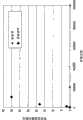
图3示出了对现有技术的液晶显示装置和本示例性实施例的液晶显示装置1所执行的按键测试的结果。通过使用直径为0.8mm的由聚缩醛(polyacetal)构成的手写笔并且通过以2.5N的力在液晶显示装置的表面上按键来执行按键测试。图3示出了基于按键次数来测量定距器层的受损个数的结果。FIG. 3 shows the results of a key test performed on the liquid crystal display device of the related art and the liquidcrystal display device 1 of the present exemplary embodiment. The key test was performed by using a stylus pen composed of polyacetal with a diameter of 0.8 mm and by pressing a key with a force of 2.5 N on the surface of the liquid crystal display device. FIG. 3 shows the results of measuring the number of damaged spacer layers based on the number of key presses.

从图3可见,在现有技术的液晶显示装置中,看到了大约一千次按键时定距器层的损坏。然而,在本示例性实施例的液晶显示装置1中,即使在一百万次按键的情况下也未看到定距器层的损坏。As can be seen from FIG. 3, in the prior art liquid crystal display device, damage to the spacer layer was seen at approximately one thousand key presses. However, in the liquidcrystal display device 1 of the present exemplary embodiment, damage to the spacer layer was not seen even in the case of one million key presses.

在现有技术的液晶显示装置中,由于定距器层和传感器调整层以非常小的接合表面与下面的层的表面紧密接触,因此剥离表面的接合表面小并且这些层容易剥离。相比之下,根据本示例性实施例的液晶显示装置1,由于分别用作定距器层21和传感器调整层22的突起部分24a和24b与平坦化膜17一体地形成,因此突起部分24a和24b与突起部分24a和24b之下的层之间的接合表面是基板的整个表面,并且剥离表面是整个表面,从而使得液晶显示装置能够抗外部压力。In the prior art liquid crystal display device, since the spacer layer and the sensor adjustment layer are in close contact with the surface of the underlying layer with a very small bonding surface, the bonding surface of the peeling surface is small and the layers are easily peeled off. In contrast, according to the liquidcrystal display device 1 of the present exemplary embodiment, since the protrudingportions 24 a and 24 b serving as thespacer layer 21 and thesensor adjustment layer 22 are integrally formed with theplanarizing film 17 , the protrudingportions 24 a The bonding surface between and 24b and the layer below the protrudingportions 24a and 24b is the entire surface of the substrate, and the peeling surface is the entire surface, thereby making the liquid crystal display device resistant to external pressure.

此外,在本示例性实施例的制造方法中,在对向基板8上,突起部分24a和24b在形成平坦化膜17的同时形成。因此,当与现有技术中分别形成平坦化膜和突起部分的方法相比,可以减少步骤数,并且本示例性实施例的制造方法在生产量和成品率方面是有利的。Furthermore, in the manufacturing method of the present exemplary embodiment, on thecounter substrate 8 , the protrudingportions 24 a and 24 b are formed simultaneously with the formation of theplanarizing film 17 . Therefore, the number of steps can be reduced when compared with the method of separately forming the planarizing film and the protruding portion in the related art, and the manufacturing method of the present exemplary embodiment is advantageous in terms of throughput and yield.

在本示例性实施例的液晶显示装置1中,使用了形成传感器电极25以用作具有传感器功能的液晶显示装置1的示例。另外,本示例性实施例可用于不具有传感器功能的液晶显示装置。此外,在本示例性实施例的液晶显示装置1中,使用了在对向基板8上形成突起部分24a和24b的示例。或者,本示例性实施例可适当地应用于以下结构:突起部分形成于面对液晶层9的表面侧上,并且也可以形成于阵列基板7的表面侧上。此外,在突起部分将要形成在阵列基板7的表面侧的情况下,与上述在对向基板8上形成突起部分24a和24b类似,可通过对由感光树脂材料形成的平坦化膜17进行曝光和显影来形成突起部分。In the liquidcrystal display device 1 of the present exemplary embodiment, an example in which thesensor electrodes 25 are formed to function as the liquidcrystal display device 1 having a sensor function is used. In addition, the present exemplary embodiment can be applied to a liquid crystal display device that does not have a sensor function. Furthermore, in the liquidcrystal display device 1 of the present exemplary embodiment, an example in which the protrudingportions 24 a and 24 b are formed on thecounter substrate 8 is used. Alternatively, the present exemplary embodiment may be suitably applied to a structure in which the protruding portion is formed on the surface side facing theliquid crystal layer 9 , and may also be formed on the surface side of thearray substrate 7 . In addition, in the case where the protruding portions are to be formed on the surface side of thearray substrate 7, similarly to the above-described formation of the protrudingportions 24a and 24b on thecounter substrate 8, it is possible to expose theplanarizing film 17 formed of a photosensitive resin material and Develop to form protrusions.

如上所述,在对向基板8或者在阵列基板7上形成的突起部分使得光在黑色显示时泄漏,并且对透射对比度比(transmission contrast ratio)具有影响。因此,通过在对向基板8或者阵列基板7中像素的非开口部分(遮光部分)中形成突起部分,可以防止对比度降低。此外,在阵列基板7的情况下,像素的非开口部分可形成在信号线上,并且在对向基板8的情况下,像素的非开口部分可形成在相邻像素之间。在信号线或者相邻像素之间的情况下,一般而言,形成信号线的金属线是0.3至1μm,因此表面升高。因此,可以使用定距器层21和传感器调整层22的高度上的表面升高部分,从而使得可以降低处理负荷。即,可以使用突起部分24a和24b的高度和阵列基板7上形成的信号线的厚度。As described above, the protruding portion formed on theopposite substrate 8 or thearray substrate 7 causes light to leak at the time of black display, and has an influence on the transmission contrast ratio. Therefore, by forming the protruding portion in the non-opening portion (light shielding portion) of the pixel in thecounter substrate 8 or thearray substrate 7, it is possible to prevent a decrease in contrast. Furthermore, in the case of thearray substrate 7 , the non-aperture portion of the pixel may be formed on the signal line, and in the case of thecounter substrate 8 , the non-aperture portion of the pixel may be formed between adjacent pixels. In the case of a signal line or between adjacent pixels, in general, the metal line forming the signal line is 0.3 to 1 μm, so the surface is raised. Therefore, a surface raised portion in the height of thespacer layer 21 and thesensor adjustment layer 22 can be used, thereby making it possible to reduce the processing load. That is, the height of the protrudingportions 24a and 24b and the thickness of the signal line formed on thearray substrate 7 can be used.

此外,通过在信号线上形成用作定距器层21的突起部分24b并且通过在除信号线之外的地方形成用作辅助定距器层22的突起部分24a,可以在同一处理中形成具有不同高度的定距器层21和辅助定距器层22。此外,当将要形成平坦化膜12时,在另一绝缘层被夹持在平坦化膜12与平坦化膜17之间的情况下形成平坦化膜12,或者在绝缘层被形成的阶段形成所需的突起部分24a和24b,从而使得可以适当地调整突起部分24a和24b的高度。In addition, by forming the protrudingportion 24b serving as thespacer layer 21 on the signal line and by forming the protrudingportion 24a serving as theauxiliary spacer layer 22 at a place other than the signal line, it is possible to form, in the same process, a Spacer layers 21 and auxiliary spacer layers 22 of different heights. Furthermore, when theplanarizing film 12 is to be formed, theplanarizing film 12 is formed with another insulating layer sandwiched between theplanarizing film 12 and theplanarizing film 17, or formed at the stage where the insulating layer is formed. Theprotrusions 24a and 24b are required so that the heights of theprotrusions 24a and 24b can be appropriately adjusted.

第二实施例second embodiment

图4示出了根据本发明第二实施例的液晶显示装置2的示意构造。本示例性实施例的液晶显示装置2是具有能够检测触摸位置的传感器功能的液晶显示装置。在本示例性实施例中,用相同的附图标记来指代与图1中相应的组件,并且省略其重复描述。FIG. 4 shows a schematic configuration of a liquidcrystal display device 2 according to a second embodiment of the present invention. The liquidcrystal display device 2 of the present exemplary embodiment is a liquid crystal display device having a sensor function capable of detecting a touched position. In this exemplary embodiment, components corresponding to those in FIG. 1 are denoted by the same reference numerals, and repeated descriptions thereof are omitted.

液晶显示装置2包括在一侧上形成有多个TFT 11的阵列基板7以及与阵列基板7相对地设置的对向基板61。然后,液晶显示装置2由阵列基板7、对向基板61和形成在这两个基板之间且具有预定厚度的液晶层9构成。The liquidcrystal display device 2 includes anarray substrate 7 formed with a plurality ofTFTs 11 on one side, and an opposingsubstrate 61 disposed opposite to thearray substrate 7. Then, the liquidcrystal display device 2 is composed of thearray substrate 7, thecounter substrate 61, and theliquid crystal layer 9 formed between these two substrates and having a predetermined thickness.

本示例性实施例的液晶显示装置2中的对向基板61除了具有分别用作定距器层21和传感器调整层22的突起部分24a和24b之外,还具有用作辅助定距器层23的突起部分24c,这些突起部分24a、24b和24c与平坦化膜17一体地形成。然后,在整个表面上除定距器层21和辅助定距器层23之外的地方顺次形成公共电极18和定向膜19。Thecounter substrate 61 in the liquidcrystal display device 2 of the present exemplary embodiment hasprotrusions 24 a and 24 b serving as thespacer layer 21 and thesensor adjustment layer 22 , respectively, and has anauxiliary spacer layer 23 . These protrudingportions 24 a , 24 b and 24 c are integrally formed with theplanarizing film 17 . Then, thecommon electrode 18 and thealignment film 19 are sequentially formed on the entire surface except for thespacer layer 21 and theauxiliary spacer layer 23 .

辅助定距器层23以略小于定距器层21的高度形成,并且用作对限定单元厚度的定距器层21的辅助。在仅增大定距器层23以防止由于施加到阵列基板7和对向基板61上的垂直外部压力而引起的液晶显示装置1的不必要的变形的构造中,形成液晶层9的液晶材料的返回将不再遵循与用于对向基板61上的绝缘层15的玻璃的变形有关的返回。如果玻璃的变形返回到原始状态的速度较快并且液晶材料返回的速度较慢,则出现在液晶层9中产生气泡的问题。相比之下,通过以小于定距器层21的高度来形成辅助定距器层23,可以获得防止在阵列基板7与对向基板61之间施加外部力时的不必要的变形的强度。此外,可以抑制由于形成绝缘基板15的玻璃和液晶层9的返回速度的差异而引起的气泡的发生。Theauxiliary spacer layer 23 is formed at a height slightly smaller than thespacer layer 21 and serves as an aid to thespacer layer 21 defining the cell thickness. In a configuration in which only thespacer layer 23 is enlarged to prevent unnecessary deformation of the liquidcrystal display device 1 due to vertical external pressure applied to thearray substrate 7 and thecounter substrate 61, the liquid crystal material forming theliquid crystal layer 9 The return of will no longer follow the return associated with the deformation of the glass used for the insulatinglayer 15 on thecounter substrate 61 . If the deformation of the glass returns to the original state faster and the return of the liquid crystal material is slower, a problem arises that air bubbles are generated in theliquid crystal layer 9 . In contrast, by forming theauxiliary spacer layer 23 at a height smaller than that of thespacer layer 21 , strength to prevent unnecessary deformation when an external force is applied between thearray substrate 7 and thecounter substrate 61 can be obtained. In addition, it is possible to suppress the occurrence of air bubbles due to the difference in the return speeds of the glass forming the insulatingsubstrate 15 and theliquid crystal layer 9 .

可通过在形成第一实施例中所述的突起部分24a和24b的步骤中将曝光步骤数增大1来在对向基板61上形成辅助定距器层23的突起部分24c。如第一实施例中所述,在通过涂布正感光树脂材料来形成感光树脂膜17a和通过对感光树脂膜17a执行曝光和显影来形成突起部分24a、24b和24c的情况下,可通过仅调整曝光量来控制突起部分24a、24b和24c的高度,从而使得更够高精度地进行控制。如上所述,在利用正感光树脂材料形成突起部分24a、24b和24c的情况下,可以独立于厚度不易控制的涂布膜来形成定距器层21、辅助定距器层23和传感器调整层22。然后,如上所述,在通过仅调整曝光量来控制突起部分24a、24b和24c的高度的情况下,在用作定距器层21和辅助定距器层23的突起部分24b和24c的高度彼此接近的情况下,也可以高精度地形成突起部分24a、24b和24c。The protrudingportion 24c of theauxiliary spacer layer 23 can be formed on thecounter substrate 61 by increasing the number of exposure steps by 1 in the step of forming the protrudingportions 24a and 24b described in the first embodiment. As described in the first embodiment, in the case of forming thephotosensitive resin film 17a by coating a positive photosensitive resin material and forming the protrudingportions 24a, 24b, and 24c by performing exposure and development on thephotosensitive resin film 17a, it is possible to The exposure amount is adjusted to control the heights of the protrudingportions 24a, 24b, and 24c, so that the control can be performed with sufficiently high precision. As described above, in the case of forming the protrudingportions 24a, 24b, and 24c using a positive photosensitive resin material, thespacer layer 21, theauxiliary spacer layer 23, and the sensor adjustment layer can be formed independently of the coating film whose thickness is not easily controlled. twenty two. Then, as described above, in the case of controlling the heights of theprotrusions 24a, 24b, and 24c by only adjusting the exposure amount, the heights of theprotrusions 24b and 24c serving as thespacer layer 21 and theauxiliary spacer layer 23 Also in the case of being close to each other, the protrudingportions 24a, 24b, and 24c can be formed with high precision.

在本示例性实施例的液晶显示装置2中,对向基板61的与液晶层9的表面相反的表面用作显示屏。此外,在本示例性实施例中,在与传感器电极25相对的位置处的像素电极13构成根据本发明一实施例的对向电极。然后,在本示例性实施例的液晶显示装置2中,对向基板61上形成的传感器电极25和阵列基板7上在与传感器电极25相对的位置处形成的像素电极13(对向电极)构成触摸传感器。In the liquidcrystal display device 2 of the present exemplary embodiment, the surface of thecounter substrate 61 opposite to the surface of theliquid crystal layer 9 functions as a display screen. Furthermore, in the present exemplary embodiment, thepixel electrode 13 at a position opposed to thesensor electrode 25 constitutes a counter electrode according to an embodiment of the present invention. Then, in the liquidcrystal display device 2 of the present exemplary embodiment, thesensor electrodes 25 formed on thecounter substrate 61 and the pixel electrodes 13 (counter electrodes) formed on thearray substrate 7 at positions opposed to thesensor electrodes 25 constitute touch sensor.

在具有以上构造的液晶显示装置2中,通过在公共电极18与像素电极13之间施加电压,改变了液晶层9的液晶的取向状态。然后,例如,从阵列基板7发出的来自光源(未示出)的光由液晶层9所调制,从而使得所需图像显示在显示屏上。In the liquidcrystal display device 2 having the above configuration, by applying a voltage between thecommon electrode 18 and thepixel electrode 13, the alignment state of the liquid crystal of theliquid crystal layer 9 is changed. Then, for example, light from a light source (not shown) emitted from thearray substrate 7 is modulated by theliquid crystal layer 9 so that desired images are displayed on the display screen.

此外,在本示例性实施例的液晶显示装置2中,例如在由诸如手或手指之类的触摸体从对向基板61外部施加压力的情况下,对向基板61朝阵列基板7弯曲。然后,在施加了压力的位置处的传感器电极25和在与传感器电极25相对的位置处的像素电极13彼此电连接。通过检测所电连接的传感器电极25和像素电极13的位置,可以检测触摸体所触摸的显示屏的位置。Further, in the liquidcrystal display device 2 of the present exemplary embodiment, the opposingsubstrate 61 bends toward thearray substrate 7 when, for example, pressure is applied from the outside of the opposingsubstrate 61 by a touch body such as a hand or a finger. Then, thesensor electrode 25 at the position where the pressure is applied and thepixel electrode 13 at the position opposed to thesensor electrode 25 are electrically connected to each other. By detecting the positions of the electrically connectedsensor electrodes 25 and thepixel electrodes 13 , the position of the display screen touched by the touch body can be detected.

第二实施例的优点Advantages of the second embodiment

根据本示例性实施例,通过与第一实施例中所描述的定距器层21和传感器调整层22类似,也与平坦化膜17一体地形成辅助定距器层23,所形成的液晶显示装置可以抗外部压力。According to this exemplary embodiment, by forming theauxiliary spacer layer 23 also integrally with theplanarizing film 17 similarly to thespacer layer 21 and thesensor adjustment layer 22 described in the first embodiment, the formed liquid crystal display The device is resistant to external pressure.

如上所述,在除了定距器层21之外还形成高度小于定距器层21的辅助定距器层23的情况下,通过也与平坦化膜17一体地形成辅助定距器层23,可以获得与第一实施例相同的优点,例如能够改善定距器层21、辅助定距器层23和传感器调整层22的剥离强度。As described above, in the case where theauxiliary spacer layer 23 having a height smaller than thespacer layer 21 is formed in addition to thespacer layer 21, by also forming theauxiliary spacer layer 23 integrally with theplanarizing film 17, The same advantages as those of the first embodiment can be obtained, for example, the peel strength of thespacer layer 21 , theauxiliary spacer layer 23 and thesensor adjustment layer 22 can be improved.

第三实施例third embodiment

图5示出了根据本发明第三实施例的液晶显示装置3的示意构造。本示例性实施例的液晶显示装置3是具有能够检测触摸位置的传感器功能的液晶显示装置。在本示例性实施例中,用相同的附图标记来指代与图1中相应的组件,并且省略其重复描述。FIG. 5 shows a schematic configuration of a liquidcrystal display device 3 according to a third embodiment of the present invention. The liquidcrystal display device 3 of the present exemplary embodiment is a liquid crystal display device having a sensor function capable of detecting a touched position. In this exemplary embodiment, components corresponding to those in FIG. 1 are denoted by the same reference numerals, and repeated descriptions thereof are omitted.

液晶显示装置3包括在一侧上形成有多个TFT 11的阵列基板7以及与阵列基板7相对地设置的对向基板26。然后,液晶显示装置3由阵列基板7、对向基板26和形成在这两个基板之间且具有预定厚度的液晶层9构成。The liquidcrystal display device 3 includes anarray substrate 7 formed with a plurality ofTFTs 11 on one side, and an opposingsubstrate 26 disposed opposite to thearray substrate 7. Then, the liquidcrystal display device 3 is constituted by thearray substrate 7, thecounter substrate 26, and theliquid crystal layer 9 formed between these two substrates and having a predetermined thickness.

在本示例性实施例的液晶显示装置3中的对向基板26上,在滤色器层16上形成具有不同高度的突起状的第一间隙调整层28、第二间隙调整层27和传感器调整层31。在本示例性实施例中,第一间隙调整层28以最高高度形成,并且第二间隙调整层27和传感器调整层31以小于第一间隙调整层28的高度形成。On theopposite substrate 26 in the liquidcrystal display device 3 of this exemplary embodiment, the protrusion-shaped firstgap adjustment layer 28 , the secondgap adjustment layer 27 and thesensor adjustment layer 28 having different heights are formed on thecolor filter layer 16 .Layer 31. In the present exemplary embodiment, the firstgap adjustment layer 28 is formed at the highest height, and the secondgap adjustment layer 27 and thesensor adjustment layer 31 are formed at a height smaller than the firstgap adjustment layer 28 .

然后,在整个表面上涂布并形成平坦化膜29以覆盖第一间隙调整层28、第二间隙调整层27和传感器调整层31。在本示例性实施例中,如上所述,各自具有预定高度的第一间隙调整层28、第二间隙调整层27和传感器调整层31由平坦化膜29所覆盖,并且与平坦化膜29一体地形成,从而形成分别具有预定高度的突起部分30a、30b和30c。即,在本示例性实施例中,第一间隙调整层28、第二间隙调整层27和传感器调整层31用作分别用于调整突起部分30a、30b和30c的高度的调整层。Then, aplanarization film 29 is coated and formed on the entire surface to cover the firstgap adjustment layer 28 , the secondgap adjustment layer 27 and thesensor adjustment layer 31 . In the present exemplary embodiment, as described above, the firstgap adjustment layer 28 , the secondgap adjustment layer 27 , and thesensor adjustment layer 31 each having a predetermined height are covered with theplanarization film 29 and are integrated with theplanarization film 29 are formed so that the protrudingportions 30a, 30b, and 30c each having a predetermined height are formed. That is, in the present exemplary embodiment, the firstgap adjustment layer 28 , the secondgap adjustment layer 27 , and thesensor adjustment layer 31 serve as adjustment layers for adjusting the heights of the protrudingportions 30 a , 30 b , and 30 c , respectively.

通过第一间隙调整层28由平坦化膜29覆盖而形成的突起部分30b用作用于保持预定单元厚度的隔离层33。此外,通过第二间隙调整层27由平坦化膜29覆盖而形成的突起部分30c用作辅助定距器层32,以便作为对减轻施加到定距器层33的外部压力的辅助。The protrudingportion 30 b formed by covering the firstgap adjustment layer 28 with theplanarizing film 29 serves as aspacer layer 33 for maintaining a predetermined cell thickness. In addition, the protrudingportion 30 c formed by covering the secondgap adjustment layer 27 with theplanarizing film 29 serves as theauxiliary spacer layer 32 as an aid for relieving external pressure applied to thespacer layer 33 .

此外,在本示例性实施例中也类似于第一和第二实施例,在整个表面上除定距器层33和辅助定距器层32之外的地方形成公共电极18和定向膜19。结果,在本示例性实施例中,通过将传感器调整层传感器调整层31由平坦化膜29所覆盖而在突起部分30a上形成的公共电极18用作传感器电极34。Further, also in this exemplary embodiment, similarly to the first and second embodiments, thecommon electrode 18 and thealignment film 19 are formed on the entire surface except for thespacer layer 33 and theauxiliary spacer layer 32 . As a result, in the present exemplary embodiment, thecommon electrode 18 formed on the protrudingportion 30 a by covering thesensor adjustment layer 31 with theplanarization film 29 is used as thesensor electrode 34 .

在本示例性实施例中,由与平坦化膜29一体地形成的传感器调整层31所形成的突起部分30a构成根据本发明一实施例的传感器调整层。In the present exemplary embodiment, the protrudingportion 30a formed by thesensor adjustment layer 31 integrally formed with theplanarization film 29 constitutes a sensor adjustment layer according to an embodiment of the present invention.

在本示例性实施例的液晶显示装置3中,对向基板26的与液晶层9的表面相反的表面用作显示屏。此外,在本示例性实施例中,在与传感器电极34相对的位置处的像素电极13构成根据本发明一实施例的对向电极。然后,在本示例性实施例的液晶显示装置3中,在对向基板26上形成的传感器电极34和在阵列基板7上在与传感器电极34相对的位置处形成的像素电极13(对向电极)构成触摸传感器。这里,触摸传感器用于检测施加到显示屏的外部压力。例如,在由诸如手或手指之类的触摸体对显示屏施加压力的情况下,可以检测触摸位置。In the liquidcrystal display device 3 of the present exemplary embodiment, the surface of thecounter substrate 26 opposite to the surface of theliquid crystal layer 9 functions as a display screen. Furthermore, in the present exemplary embodiment, thepixel electrode 13 at a position opposed to thesensor electrode 34 constitutes a counter electrode according to an embodiment of the present invention. Then, in the liquidcrystal display device 3 of the present exemplary embodiment, thesensor electrodes 34 formed on thecounter substrate 26 and the pixel electrodes 13 (thecounter electrodes 34 formed on thearray substrate 7 at positions opposite to the sensor electrodes 34 ) form the touch sensor. Here, the touch sensor is used to detect external pressure applied to the display screen. For example, in the case where pressure is applied to the display screen by a touch body such as a hand or a finger, a touch position can be detected.

在具有以上构造的液晶显示装置3中,通过在公共电极18与像素电极13之间施加电压,改变了液晶层9的液晶的取向状态。然后,例如,从阵列基板7发出的来自光源(未示出)的光由液晶层9所调制,从而使得所需图像显示在显示屏上。In the liquidcrystal display device 3 having the above configuration, by applying a voltage between thecommon electrode 18 and thepixel electrode 13, the alignment state of the liquid crystal of theliquid crystal layer 9 is changed. Then, for example, light from a light source (not shown) emitted from thearray substrate 7 is modulated by theliquid crystal layer 9 so that desired images are displayed on the display screen.

此外,在本示例性实施例的液晶显示装置3中,例如在由诸如手或手指之类的触摸体从对向基板26外部施加压力的情况下,对向基板26朝阵列基板7弯曲。然后,在施加了压力的位置处的传感器电极34和在与传感器电极34相对的位置处的像素电极13彼此电连接。通过检测所电连接的传感器电极34和像素电极13的位置,可以检测触摸体所触摸的显示屏的位置。Further, in the liquidcrystal display device 3 of the present exemplary embodiment, the opposingsubstrate 26 bends toward thearray substrate 7 when, for example, pressure is applied from the outside of the opposingsubstrate 26 by a touch body such as a hand or a finger. Then, thesensor electrode 34 at the position where the pressure is applied and thepixel electrode 13 at the position opposed to thesensor electrode 34 are electrically connected to each other. By detecting the positions of the electrically connectedsensor electrodes 34 and thepixel electrodes 13 , the position of the display screen touched by the touch body can be detected.

第三实施例的优点Advantages of the third embodiment

根据本示例性实施例的液晶显示装置3,突起部分30a、30b和30c由传感器调整层31、第一间隙调整层28、第二间隙调整层27和覆盖这些调整层形成的平坦化膜29形成。如上所述,由于突起部分30a、30b和30c由在基板的整个表面上形成的平坦化膜29所覆盖并且与平坦化膜29一体地形成,因此突起部分30a、30b和30c与突起部分30a、30b和30c之下的层的表面相接合的区域是基板的整个表面。因此,由于突起部分30a、30b和30c的剥离表面是基板的整个表面,因此获得与第一实施例相同的优点,例如能够改善突起部分30a、30b和30c的剥离强度。According to the liquidcrystal display device 3 of the present exemplary embodiment, the protrudingportions 30a, 30b, and 30c are formed of thesensor adjustment layer 31, the firstgap adjustment layer 28, the secondgap adjustment layer 27, and theplanarization film 29 formed to cover these adjustment layers . As described above, since the protrudingportions 30a, 30b, and 30c are covered by theplanarizing film 29 formed on the entire surface of the substrate and integrally formed with theplanarizing film 29, the protrudingportions 30a, 30b, and 30c are closely related to the protrudingportions 30a, 30a, and 30c. The area where the surfaces of the layers below 30b and 30c join is the entire surface of the substrate. Therefore, since the peeling surface of theprotrusions 30a, 30b, and 30c is the entire surface of the substrate, the same advantages as those of the first embodiment are obtained, for example, the peeling strength of theprotrusions 30a, 30b, and 30c can be improved.

此外,在本示例性实施例中,虽然突起部分30a、30b和30c与平坦化膜29一体地形成,但是突起部分30a、30b和30c不是共同形成的。因此,对于用于调整突起部分30a、30b和30c的高度的传感器调整层31、第一间隙调整层28和第二间隙调整层27,可以使用不透明材料,例如,诸如信号线之类的金属材料、诸如彩色抗蚀剂(colored resist)之类的负抗蚀剂、酚醛正抗蚀剂或者丙烯酸抗蚀剂。此外,因为平坦化膜29在上部单独形成,所以平坦性的问题和对离子进行脱气(degass)的问题并不十分重要。因此,形成第一间隙调整层28、第二间隙调整层27和传感器调整层31的材料的选择数增多。Furthermore, in the present exemplary embodiment, although the protrudingportions 30 a , 30 b , and 30 c are formed integrally with theplanarizing film 29 , the protrudingportions 30 a , 30 b , and 30 c are not commonly formed. Therefore, for thesensor adjustment layer 31, the firstgap adjustment layer 28, and the secondgap adjustment layer 27 for adjusting the heights of the protrudingportions 30a, 30b, and 30c, an opaque material such as a metal material such as a signal line can be used. , a negative resist such as a colored resist, a phenolic positive resist, or an acrylic resist. In addition, since theplanarizing film 29 is formed separately on the upper portion, the problem of flatness and the problem of degassing ions are not so important. Therefore, the number of choices of materials for forming the firstgap adjustment layer 28 , the secondgap adjustment layer 27 , and thesensor adjustment layer 31 increases.

可通过在整个表面上涂布相同材料并且通过改变曝光次数来形成第一间隙调整层28、第二间隙调整层27和传感器调整层31。或者,也可以通过使用不同材料来形成第一间隙调整层28、第二间隙调整层27和传感器调整层31。此外,也可以在不同层上形成第一间隙调整层28、第二间隙调整层27和传感器调整层31。在第一间隙调整层28、第二间隙调整层27和传感器调整层31用相同材料形成的情况下,可以减少步骤数。The firstgap adjustment layer 28, the secondgap adjustment layer 27, and thesensor adjustment layer 31 may be formed by coating the same material on the entire surface and by changing the number of exposures. Alternatively, the firstgap adjustment layer 28 , the secondgap adjustment layer 27 , and thesensor adjustment layer 31 may also be formed by using different materials. In addition, the firstgap adjustment layer 28, the secondgap adjustment layer 27, and thesensor adjustment layer 31 may be formed on different layers. In the case where the firstgap adjustment layer 28 , the secondgap adjustment layer 27 , and thesensor adjustment layer 31 are formed of the same material, the number of steps can be reduced.

第四实施例Fourth embodiment

图6示出了根据本发明第四实施例的液晶显示装置4的示意构造。本示例性实施例的液晶显示装置4是具有能够检测触摸位置的传感器功能的液晶显示装置。在本示例性实施例中,用相同的附图标记来指代与图1中相应的组件,并且省略其重复描述。FIG. 6 shows a schematic configuration of a liquid crystal display device 4 according to a fourth embodiment of the present invention. The liquid crystal display device 4 of the present exemplary embodiment is a liquid crystal display device having a sensor function capable of detecting a touched position. In this exemplary embodiment, components corresponding to those in FIG. 1 are denoted by the same reference numerals, and repeated descriptions thereof are omitted.

液晶显示装置4包括在一侧上形成有多个TFT 11的阵列基板35以及与阵列基板35相对地设置的对向基板36。然后,液晶显示装置4由阵列基板35、对向基板36和形成在这两个基板之间且具有预定厚度的液晶层9构成。The liquid crystal display device 4 includes anarray substrate 35 formed with a plurality ofTFTs 11 on one side, and an opposingsubstrate 36 disposed opposite to thearray substrate 35. Then, the liquid crystal display device 4 is constituted by anarray substrate 35 , acounter substrate 36 , and aliquid crystal layer 9 formed between these two substrates and having a predetermined thickness.

阵列基板35配置为包括由透明矩形平板状玻璃形成的绝缘基板10和在绝缘基板10的面对液晶层9的表面上形成的多个TFT 11。此外,在绝缘基板10的面对液晶层9的表面上与传感器电极(稍后描述)相对的位置处形成突起状的第一传感器调整层37。然后,以覆盖TFT 11和第一传感器调整层37的方式在绝缘基板10的整个表面上形成平坦化膜62,并且在平坦化膜62上形成接触部分14,TFT 11的一部分从各个接触部分14露出。平坦化膜62形成为使得阵列基板35的面对液晶层9的表面上除接触部分14和第一传感器调整层37的部分平坦化。第一传感器调整层37和其上形成的平坦化膜62构成突起部分41。Thearray substrate 35 is configured to include an insulatingsubstrate 10 formed of transparent rectangular flat glass and a plurality ofTFTs 11 formed on a surface of the insulatingsubstrate 10 facing theliquid crystal layer 9. Further, a protrusion-shaped firstsensor adjustment layer 37 is formed at a position opposed to a sensor electrode (described later) on the surface of the insulatingsubstrate 10 facing theliquid crystal layer 9 . Then, aplanarizing film 62 is formed on the entire surface of the insulatingsubstrate 10 in such a manner as to cover theTFT 11 and the firstsensor adjustment layer 37, andcontact portions 14 are formed on theplanarizing film 62, and a part of theTFT 11 is connected from eachcontact portion 14. exposed. Theplanarizing film 62 is formed to planarize a portion of the surface of thearray substrate 35 facing theliquid crystal layer 9 except for thecontact portion 14 and the firstsensor adjustment layer 37 . The firstsensor adjustment layer 37 and theplanarization film 62 formed thereon constitute the protrudingportion 41 .

然后,以对应于平坦化膜62上各像素的方式按图案形成像素电极13。各像素电极13通过平坦化膜62上形成的接触部分14连接到作为开关元件的TFT 11。像素电极13用作透明电极并且例如由ITO(氧化铟锡)形成。在本示例性实施例中,在突起部分41上形成的像素电极13用作第一传感器电极43a。Then, thepixel electrodes 13 are patterned to correspond to the respective pixels on theplanarizing film 62 . Eachpixel electrode 13 is connected to aTFT 11 as a switching element through acontact portion 14 formed on theplanarizing film 62. Thepixel electrode 13 serves as a transparent electrode and is formed of, for example, ITO (Indium Tin Oxide). In the present exemplary embodiment, thepixel electrode 13 formed on the protrudingportion 41 serves as thefirst sensor electrode 43a.

此外,在像素电极13上的预定位置处形成定距器层44。该定距器层44形成为保持液晶层9的厚度(即,单元厚度)以便在平面内恒定,并且以单元厚度达到预定厚度的高度形成。In addition, aspacer layer 44 is formed at a predetermined position on thepixel electrode 13 . Thespacer layer 44 is formed to maintain the thickness of the liquid crystal layer 9 (ie, cell thickness) so as to be constant in a plane, and is formed at a height at which the cell thickness reaches a predetermined thickness.

此外,在像素电极13上,在覆盖像素电极13的整个表面上形成定向膜20。Further, on thepixel electrode 13 , analignment film 20 is formed covering the entire surface of thepixel electrode 13 .

对向基板36由透明绝缘基板15(例如玻璃或者聚碳酸酯(PC))、在绝缘基板15的面对液晶层9的表面上形成的滤色层16、在滤色层16上的预定位置处形成的第二传感器调整层38和平坦化膜39构成。Theopposite substrate 36 is made of a transparent insulating substrate 15 (such as glass or polycarbonate (PC)), acolor filter layer 16 formed on the surface of the insulatingsubstrate 15 facing theliquid crystal layer 9, and a predetermined position on thecolor filter layer 16. The secondsensor adjustment layer 38 and theplanarization film 39 formed therein are formed.

第二传感器调整层38以突起状的形式形成。The secondsensor adjustment layer 38 is formed in a protrusion shape.

平坦化膜39形成在整个表面上以覆盖第二传感器调整层38,并且该平坦化膜39使得像素的开口部分能够平坦化。然后,第二传感器调整层38和其上形成的平坦化膜39构成突起部分42。Aplanarization film 39 is formed on the entire surface to cover the secondsensor adjustment layer 38 , and thisplanarization film 39 enables the opening portion of the pixel to be planarized. Then, the secondsensor adjustment layer 38 and theplanarization film 39 formed thereon constitute the protrudingportion 42 .

然后,在平坦化膜39的整个表面上形成公共电极18,并且在公共电极18上形成定向膜19。在本示例性实施例中,突起部分42上形成的公共电极18用作第二传感器电极43b。Then, thecommon electrode 18 is formed on the entire surface of theplanarizing film 39 , and thealignment film 19 is formed on thecommon electrode 18 . In the present exemplary embodiment, thecommon electrode 18 formed on the protrudingportion 42 serves as thesecond sensor electrode 43b.

在本示例性实施例中,由分别与平坦化膜62和39一体地形成的第一传感器调整层37和第二传感器调整层38所形成的突起部分41和42构成根据本发明一实施例的传感器调整层。In the present exemplary embodiment, the protrudingportions 41 and 42 formed by the firstsensor adjustment layer 37 and the secondsensor adjustment layer 38 formed integrally with theplanarization films 62 and 39 respectively constitute a sensor according to an embodiment of the present invention. Sensor adjustment layer.

此外,在本示例性实施例中,液晶层9以如下方式形成:层压阵列基板35和对向基板36,并且在阵列基板35和对向基板36之间密封液晶,其中使用定距器层44来保持预定的单元厚度并且定向膜19和20向内面对。Furthermore, in this exemplary embodiment, theliquid crystal layer 9 is formed by laminating thearray substrate 35 and thecounter substrate 36 and sealing the liquid crystal between thearray substrate 35 and thecounter substrate 36 using aspacer layer 44 to maintain a predetermined cell thickness and theorientation films 19 and 20 face inwardly.

第一传感器调整层37和第二传感器调整层38形成为分别用于调整突起部分41和42的高度的调整层,即,设置为用于调整第一传感器电极43a与第二传感器电极43b之间的距离的层。在未将外部压力施加到液晶显示装置4的状态下,有必要使得第一传感器电极43a和第二传感器电极43b不连接。因此,第一传感器调整层37和第二传感器调整层38以如下高度设定:在这些高度,第一传感器电极43a在定距器层44所保持的单元厚度下不接触与第一传感器电极相对的第二传感器电极43b。The firstsensor adjustment layer 37 and the secondsensor adjustment layer 38 are formed as adjustment layers for adjusting the heights of the protrudingportions 41 and 42, respectively, that is, provided for adjusting the height between thefirst sensor electrode 43a and thesecond sensor electrode 43b. layer of distance. In a state where no external pressure is applied to the liquid crystal display device 4 , it is necessary for thefirst sensor electrode 43 a and thesecond sensor electrode 43 b to be disconnected. Therefore, the firstsensor adjustment layer 37 and the secondsensor adjustment layer 38 are set at heights at which thefirst sensor electrodes 43a do not contact the opposite first sensor electrodes under the unit thickness maintained by thespacer layer 44. Thesecond sensor electrode 43b.

在本示例性实施例中,第二传感器电极43b构成根据本发明一实施例的对向电极。In this exemplary embodiment, thesecond sensor electrode 43b constitutes a counter electrode according to an embodiment of the present invention.

在本示例性实施例的液晶显示装置4中,对向基板35的与液晶层9的表面相反的表面用作显示屏。此外,在本示例性实施例中,在与另一传感器电极相对的位置处的一个传感器电极构成根据本发明一实施例的对向电极。此外,在本示例性实施例的液晶显示装置4中,阵列基板35上形成的第一传感器电极43a和对向基板36上在与第一传感器电极43a相对的位置处形成的第二传感器电极43b(对向电极)构成触摸传感器。这里,触摸传感器用于检测施加到显示屏的外部压力。例如,在由诸如手或手指之类的触摸体对显示屏施加压力的情况下,触摸传感器可以检测触摸位置。In the liquid crystal display device 4 of the present exemplary embodiment, the surface of thecounter substrate 35 opposite to the surface of theliquid crystal layer 9 functions as a display screen. Furthermore, in the present exemplary embodiment, one sensor electrode at a position opposed to another sensor electrode constitutes a counter electrode according to an embodiment of the present invention. Furthermore, in the liquid crystal display device 4 of the present exemplary embodiment, thefirst sensor electrode 43 a formed on thearray substrate 35 and thesecond sensor electrode 43 b formed on thecounter substrate 36 at a position opposite to thefirst sensor electrode 43 a (Counter electrode) constitutes a touch sensor. Here, the touch sensor is used to detect external pressure applied to the display screen. For example, in a case where pressure is applied to the display screen by a touch body such as a hand or a finger, the touch sensor can detect a touch position.

在具有以上构造的液晶显示装置4中,通过在公共电极18与像素电极13之间施加电压,改变了液晶层9的液晶的取向状态。然后,例如,调制从阵列基板35发出的来自光源(未示出)的光,从而使得所需图像显示在显示屏上。In the liquid crystal display device 4 having the above configuration, by applying a voltage between thecommon electrode 18 and thepixel electrode 13, the alignment state of the liquid crystal of theliquid crystal layer 9 is changed. Then, for example, light from a light source (not shown) emitted from thearray substrate 35 is modulated so that a desired image is displayed on the display screen.

此外,在本示例性实施例的液晶显示装置4中,例如在由诸如手或手指之类的触摸体从对向基板36外部施加压力的情况下,对向基板36朝阵列基板35弯曲。然后,在施加了压力的位置处的第一传感器电极43a和在与第一传感器电极43a相对的位置处的第二传感器电极43b电连接。通过检测电连接的第一传感器电极43a和第二传感器电极43b的位置,可以检测触摸体所触摸的显示屏的位置。Furthermore, in the liquid crystal display device 4 of the present exemplary embodiment, the opposingsubstrate 36 bends toward thearray substrate 35 when, for example, pressure is applied from the outside of the opposingsubstrate 36 by a touch body such as a hand or a finger. Then, thefirst sensor electrode 43a at the position where the pressure is applied and thesecond sensor electrode 43b at the position opposite to thefirst sensor electrode 43a are electrically connected. By detecting the positions of thefirst sensor electrode 43 a and thesecond sensor electrode 43 b that are electrically connected, the position of the display screen touched by the touch body can be detected.

第四实施例的优点Advantages of the fourth embodiment

在本示例性实施例的液晶显示装置4中,通过在对向基板36和阵列基板35二者上形成突起部分41和42,即使在由于平坦化膜62和39的材料特性而难以充分实现突起部分41和42的高度的情况下,也可以形成能够高精度地呈现传感器功能的液晶显示装置4。In the liquid crystal display device 4 of the present exemplary embodiment, by forming the protrudingportions 41 and 42 on both thecounter substrate 36 and thearray substrate 35, even when it is difficult to sufficiently realize the protruding parts due to the material characteristics of the planarizingfilms 62 and 39 Even when the height of theparts 41 and 42 is lower, the liquid crystal display device 4 capable of exhibiting the sensor function with high precision can be formed.

然后,在本示例性实施例中,与第三实施例类似,由第一传感器调整层37、第二传感器调整层38以及覆盖这些调整层形成的平坦化膜62和39形成突起部分41和42。如上所述,由于突起部分41和42分别由基板的整个表面上形成的平坦化膜62和39所覆盖并且与平坦化膜62和39一体地形成,因此突起部分41和42与突起部分41和42之下的层的表面相接合的区域是基板的整个表面。因此,由于突起部分41和42的剥离表面是基板的整个表面,因此获得诸如能够改善突起部分41和42的剥离强度之类的优点。Then, in the present exemplary embodiment, similarly to the third embodiment, theprotrusions 41 and 42 are formed by the firstsensor adjustment layer 37, the secondsensor adjustment layer 38, and theplanarization films 62 and 39 formed to cover these adjustment layers. . As described above, since the protrudingparts 41 and 42 are respectively covered by the planarizingfilms 62 and 39 formed on the entire surface of the substrate and integrally formed with the planarizingfilms 62 and 39, the protrudingparts 41 and 42 are closely related to the protrudingparts 41 and 39. The area where the surfaces of the layers below 42 are joined is the entire surface of the substrate. Therefore, since the peeling surface of theprotrusions 41 and 42 is the entire surface of the substrate, an advantage is obtained such that the peeling strength of theprotrusions 41 and 42 can be improved.

在本示例性实施例中,描述了如下示例:形成突起状的第一传感器调整层37和第二传感器调整层38,此后形成平坦化膜62和39以分别形成突起部分41和42。另外,与第一实施例类似,通过对感光树脂膜进行曝光和显影,可以提供与第一传感器调整层37、第二传感器调整层38以及平坦化膜62和39一体地形成的突起部分41和42。如上所述,在由于厚膜而应用太多步进节拍(stepper tact)的情况下,将第一传感器调整层37和第二传感器调整层38分别与平坦化膜62和39共同形成的方法是有效的。此外,该方法也有效地用于以下情况:难以将用作平坦化膜62和39的涂敷材料很好地涂布成第一传感器调整层37和第二传感器调整层38的形状。此外,该方法对于难以通过回流来很好地形成突起部分41和42的形状的情况也是有效的。In this exemplary embodiment, an example is described in which the protrusion-shaped firstsensor adjustment layer 37 and the secondsensor adjustment layer 38 are formed, and thereafter theplanarization films 62 and 39 are formed to form theprotrusion portions 41 and 42 , respectively. In addition, similarly to the first embodiment, by exposing and developing a photosensitive resin film, it is possible to provide the protrudingportion 41 and the protrudingportion 41 integrally formed with the firstsensor adjustment layer 37, the secondsensor adjustment layer 38, and the planarizingfilms 62 and 39. 42. As described above, in the case where too much stepper tact is applied due to thick films, the method of forming the firstsensor adjustment layer 37 and the secondsensor adjustment layer 38 together with theplanarization films 62 and 39, respectively, is Effective. In addition, this method is also effective for the case where it is difficult to coat the coating material serving as theplanarization films 62 and 39 well into the shapes of the firstsensor adjustment layer 37 and the secondsensor adjustment layer 38 . Furthermore, this method is also effective for cases where it is difficult to form the shapes of the protrudingportions 41 and 42 well by reflow.

第五实施例fifth embodiment

图7示出了根据本发明第五实施例的液晶显示装置5的示意构造。本示例性实施例的液晶显示装置5是具有能够检测触摸位置的传感器功能的液晶显示装置。在本示例性实施例中,用相同的附图标记来指代与图1中相应的组件,并且省略其重复描述。FIG. 7 shows a schematic configuration of a liquidcrystal display device 5 according to a fifth embodiment of the present invention. The liquidcrystal display device 5 of the present exemplary embodiment is a liquid crystal display device having a sensor function capable of detecting a touched position. In this exemplary embodiment, components corresponding to those in FIG. 1 are denoted by the same reference numerals, and repeated descriptions thereof are omitted.

液晶显示装置5包括在一侧上形成有多个TFT 11的阵列基板45以及与阵列基板45相对地设置的对向基板46。然后,液晶显示装置5由阵列基板45、对向基板46和形成在这两个基板之间且具有预定厚度的液晶层9构成。The liquidcrystal display device 5 includes an array substrate 45 formed with a plurality ofTFTs 11 on one side, and an opposing substrate 46 disposed opposite to the array substrate 45. Then, the liquidcrystal display device 5 is constituted by an array substrate 45, a counter substrate 46, and aliquid crystal layer 9 formed between these two substrates and having a predetermined thickness.

阵列基板45配置为包括由透明矩形平板状玻璃形成的绝缘基板10和在绝缘基板10的面对液晶层9的表面上形成的多个TFT 11。多个TFT 11以对应于像素的方式按阵列状设置。The array substrate 45 is configured to include an insulatingsubstrate 10 formed of transparent rectangular flat glass and a plurality ofTFTs 11 formed on a surface of the insulatingsubstrate 10 facing theliquid crystal layer 9. A plurality ofTFTs 11 are arranged in an array corresponding to pixels.

然后,以覆盖TFT 11方式在绝缘基板10的整个表面上形成平坦化膜72。在平坦化膜72上形成接触部分14(TFT 11的一部分从各个接触部分14露出),并且还在与对向基板46上形成的传感器电极(稍后描述)相对应的位置处形成具有预定深度的凹槽部分48。平坦化膜72形成为使得阵列基板45的面对液晶层9的表面上除接触部分14和凹槽部分48(即,像素的开口部分)之外的部分平坦化。Then, a planarizing film 72 is formed on the entire surface of the insulatingsubstrate 10 so as to cover theTFT 11. The contact portions 14 (a part of theTFT 11 is exposed from each contact portion 14) are formed on the planarizing film 72, and a sensor electrode having a predetermined depth is also formed at a position corresponding to a sensor electrode (described later) formed on the counter substrate 46. The groove part 48. The planarizing film 72 is formed to planarize the portion on the surface of the array substrate 45 facing theliquid crystal layer 9 except thecontact portion 14 and the groove portion 48 (ie, the opening portion of the pixel).

此外,在平坦化膜72上以对应于各像素的方式按图案形成像素电极58。此时,在平坦化膜72上形成的凹槽部分48内也形成像素电极58。各像素电极58通过在平坦化膜72上形成的接触部分14而连接到作为开关元件的TFT 11。这些像素电极58形成为透明电极,并且例如利用ITO(氧化铟锡)形成。In addition, the pixel electrodes 58 are formed in a pattern corresponding to each pixel on the planarization film 72 . At this time, the pixel electrode 58 is also formed in the groove portion 48 formed on the planarizing film 72 . Each pixel electrode 58 is connected to theTFT 11 as a switching element through thecontact portion 14 formed on the planarizing film 72. These pixel electrodes 58 are formed as transparent electrodes, and are formed using ITO (Indium Tin Oxide), for example.

然后,以覆盖像素电极58的方式在像素电极58的整个表面上形成定向膜49。然后,凹槽部分48的深度使得当形成像素电极58和定向膜49时,这些不被完全掩埋。Then, an alignment film 49 is formed on the entire surface of the pixel electrode 58 so as to cover the pixel electrode 58 . Then, the depth of the groove portion 48 is such that when the pixel electrode 58 and the alignment film 49 are formed, these are not completely buried.

对向基板46由透明绝缘基板15(例如玻璃或者聚碳酸酯(PC))、在绝缘基板15的面对液晶层9的表面上形成的滤色层16和在滤色层16上形成的平坦化膜47构成。然后,对向基板46具有与平坦化膜47一体地形成的突起部分50a和50b。在本示例性实施例中,突起部分50a和50b分别构成传感器调整层51和定距器层52。在整个表面上除定距器层52之外的地方形成公共电极59,并且在公共电极59上形成定向膜60。The opposite substrate 46 is made of a transparent insulating substrate 15 (such as glass or polycarbonate (PC)), acolor filter layer 16 formed on the surface of the insulatingsubstrate 15 facing theliquid crystal layer 9, and a flat surface formed on thecolor filter layer 16. Chemical film 47 constitutes. Then, the counter substrate 46 has protruding portions 50 a and 50 b integrally formed with the planarization film 47 . In the present exemplary embodiment, the protruding portions 50 a and 50 b constitute thesensor adjustment layer 51 and thespacer layer 52 , respectively. Thecommon electrode 59 is formed on the entire surface except thespacer layer 52 , and the alignment film 60 is formed on thecommon electrode 59 .

定距器层52形成为使得液晶层9的厚度(即,单元厚度)得以保持以便在平面内恒定,并且以单元厚度达到预定厚度的高度形成。Thespacer layer 52 is formed such that the thickness of the liquid crystal layer 9 (ie, cell thickness) is maintained so as to be constant in a plane, and is formed at a height at which the cell thickness reaches a predetermined thickness.

然后,在本示例性实施例中,传感器调整层51也以与定距器层52相同的高度形成,并且在传感器调整层51上形成的公共电极59用作传感器电极53。此外,关于在与传感器电极53(利用在传感器调整层51上形成的公共电极59所形成)相对的位置处的阵列基板45,在平坦化膜72上形成凹槽部分48并且以进入凹槽部分48的方式形成像素电极58。因此,在未施加外部力的状态下,传感器电极53和像素电极58彼此并不连接。此外,在本示例性实施例中,在与传感器电极53相对的位置处的像素电极58构成根据本发明一实施例的对向电极。在本示例性实施例中,传感器电极53和在与传感器电极53相对的阵列基板45的凹槽部分48中所形成的像素电极58(对向电极)构成触摸传感器。Then, in the present exemplary embodiment, thesensor adjustment layer 51 is also formed at the same height as thespacer layer 52 , and thecommon electrode 59 formed on thesensor adjustment layer 51 serves as thesensor electrode 53 . Further, with respect to the array substrate 45 at a position opposed to the sensor electrode 53 (formed with thecommon electrode 59 formed on the sensor adjustment layer 51), the groove portion 48 is formed on the planarizing film 72 and to enter the groove portion 48 to form the pixel electrode 58 . Therefore, in a state where no external force is applied, thesensor electrode 53 and the pixel electrode 58 are not connected to each other. Furthermore, in the present exemplary embodiment, the pixel electrode 58 at a position opposed to thesensor electrode 53 constitutes a counter electrode according to an embodiment of the present invention. In the present exemplary embodiment, thesensor electrodes 53 and the pixel electrodes 58 (counter electrodes) formed in the groove portions 48 of the array substrate 45 opposite to thesensor electrodes 53 constitute a touch sensor.

在具有以上构造的液晶显示装置5中,通过在公共电极59与像素电极58之间施加电压,改变了液晶层9的液晶的取向状态,并且显示所需图像。此外,在本示例性实施例的液晶显示装置5中,例如在由诸如手或手指之类的触摸体从对向基板46外部施加压力的情况下,对向基板46朝阵列基板45弯曲,并且在施加了压力的位置处的传感器电极53进入阵列基板45上形成的凹槽部分48并与凹槽部分48中形成的像素电极58电连接。通过检测电连接的传感器电极53和像素电极58的位置,可以检测触摸体所触摸的触摸位置。In the liquidcrystal display device 5 having the above configuration, by applying a voltage between thecommon electrode 59 and the pixel electrode 58, the alignment state of the liquid crystal of theliquid crystal layer 9 is changed, and a desired image is displayed. Furthermore, in the liquidcrystal display device 5 of the present exemplary embodiment, for example, in the case where pressure is applied from the outside of the opposing substrate 46 by a touch body such as a hand or a finger, the opposing substrate 46 is bent toward the array substrate 45, and Thesensor electrode 53 at the position where the pressure is applied enters the groove portion 48 formed on the array substrate 45 and is electrically connected to the pixel electrode 58 formed in the groove portion 48 . By detecting the positions of the electrically connectedsensor electrodes 53 and the pixel electrodes 58 , it is possible to detect the touch position touched by the touch body.

第五实施例的优点Advantages of the fifth embodiment

在本示例性实施例的液晶显示装置5中,在对向基板46上形成的分别用作传感器调整层51和定距器层52的突起部分50a和50b与平坦化膜47一体地形成。因此,对向基板46与定距器层52和传感器调整层51的接触程度增大,使得由于对液晶显示装置5施加压力所引起的定距器层52和传感器调整层51的剥离被降低。In the liquidcrystal display device 5 of the present exemplary embodiment, the protruding portions 50 a and 50 b formed on the counter substrate 46 and serving as thesensor adjustment layer 51 and thespacer layer 52 , respectively, are integrally formed with the planarizing film 47 . Therefore, the degree of contact of the counter substrate 46 with thespacer layer 52 and thesensor adjustment layer 51 is increased, so that peeling of thespacer layer 52 and thesensor adjustment layer 51 due to pressure applied to the liquidcrystal display device 5 is reduced.

此外,根据本示例性实施例的液晶显示装置5,由于传感器调整层51以与用于定义单元厚度的定距器层52相同的高度形成,因此不必要诸如两次曝光之类的步骤。因此,可以在不增加步骤数的情况下形成传感器调整层51。Furthermore, according to the liquidcrystal display device 5 of the present exemplary embodiment, since thesensor adjustment layer 51 is formed at the same height as thespacer layer 52 for defining the cell thickness, steps such as double exposure are unnecessary. Therefore, thesensor adjustment layer 51 can be formed without increasing the number of steps.

第六实施例Sixth embodiment

图8示出了根据本发明第六实施例的液晶显示装置6的示意构造。本示例性实施例的液晶显示装置6是具有能够检测触摸位置的传感器功能的液晶显示装置。在本示例性实施例中,用相同的附图标记来指代与图1中相应的组件,并且省略其重复描述。FIG. 8 shows a schematic configuration of a liquidcrystal display device 6 according to a sixth embodiment of the present invention. The liquidcrystal display device 6 of the present exemplary embodiment is a liquid crystal display device having a sensor function capable of detecting a touched position. In this exemplary embodiment, components corresponding to those in FIG. 1 are denoted by the same reference numerals, and repeated descriptions thereof are omitted.

液晶显示装置6包括在一侧上形成有多个TFT 11的阵列基板51以及与阵列基板51相对地设置的对向基板50。然后,液晶显示装置6由阵列基板51、对向基板50和形成在这两个基板之间且具有预定厚度的液晶层9构成。The liquidcrystal display device 6 includes anarray substrate 51 formed with a plurality ofTFTs 11 on one side, and an opposingsubstrate 50 disposed opposite to thearray substrate 51. Then, the liquidcrystal display device 6 is constituted by anarray substrate 51 , acounter substrate 50 , and aliquid crystal layer 9 formed between these two substrates and having a predetermined thickness.

阵列基板51配置为包括由透明矩形平板状玻璃形成的绝缘基板10和在绝缘基板10的面对液晶层9的表面上形成的多个TFT 11。多个TFT 11以对应于像素的方式按阵列状设置。然后,以覆盖TFT 11方式在绝缘基板10的整个表面上形成平坦化膜63,并且形成与平坦化膜63一体地形成的突起部分67a和67b。突起部分67a用作传感器调整层64,并且突起部分67b用作定距器层54。在平坦化膜63上除定距器层54之外的地方形成公共电极56。然后,在公共电极56的整个表面上除定距器层54之外的地方形成中间层绝缘膜59,并且在中间层绝缘膜59上形成与各像素相对应的像素电极57。通过形成为经过中间层绝缘膜59和平坦化膜63的接触部分14,像素电极57连接到TFT 11。此外,此时为了使像素电极57和公共电极56在接触部分14中不短路,在平坦化膜63和传感器调整层64上除接触部分14之外的地方形成公共电极56。然后,以覆盖像素电极57的方式形成定向膜20。此外,与本示例性实施例的平坦化膜63一体地形成的突起部分67a和在突起部分67a上形成的中间层绝缘膜59构成突起部分66(由多层形成)。Thearray substrate 51 is configured to include an insulatingsubstrate 10 formed of transparent rectangular flat glass and a plurality ofTFTs 11 formed on a surface of the insulatingsubstrate 10 facing theliquid crystal layer 9. A plurality ofTFTs 11 are arranged in an array corresponding to pixels. Then, aplanarizing film 63 is formed on the entire surface of the insulatingsubstrate 10 in such a manner as to cover theTFT 11, and protruding portions 67a and 67b integrally formed with theplanarizing film 63 are formed. The protruding portion 67 a serves as the sensor adjustment layer 64 , and the protruding portion 67 b serves as the spacer layer 54 . Thecommon electrode 56 is formed on theplanarizing film 63 except for the spacer layer 54 . Then, aninterlayer insulating film 59 is formed on the entire surface of thecommon electrode 56 except for the spacer layer 54 , and apixel electrode 57 corresponding to each pixel is formed on theinterlayer insulating film 59 . Thepixel electrode 57 is connected to theTFT 11 through thecontact portion 14 formed through theinterlayer insulating film 59 and theplanarizing film 63. Also, at this time, in order not to short-circuit thepixel electrode 57 and thecommon electrode 56 in thecontact portion 14 , thecommon electrode 56 is formed on theplanarizing film 63 and the sensor adjustment layer 64 except for thecontact portion 14 . Then, thealignment film 20 is formed so as to cover thepixel electrodes 57 . Further, the protruding portion 67a formed integrally with theplanarizing film 63 of this exemplary embodiment and theinterlayer insulating film 59 formed on the protruding portion 67a constitute the protruding portion 66 (formed of multiple layers).

定距器层54形成为使得厚度(即,单元厚度)得以保持以便在平面内恒定,并且以单元厚度达到预定厚度的高度形成。因此,与平坦化膜63一体地形成的定距器层54以如下高度以突起状的形式形成:该高度使得当在平坦化膜63上形成公共电极56、中间层绝缘膜59、像素电极57和定向膜20时,足以具有作为液晶层9的单元厚度的充分高度。此外,传感器调整层64形成为低于定距器层54,并且在传感器调整层64和包括中间层绝缘膜在内的突起部分66上形成的像素电极57用作传感器电极65。即,传感器调整层64用于实现传感器电极65的高度。在本示例性实施例中,突起部分66构成根据本发明一实施例的传感器调整层。The spacer layer 54 is formed such that the thickness (ie, cell thickness) is maintained so as to be constant in a plane, and is formed at a height at which the cell thickness reaches a predetermined thickness. Therefore, the spacer layer 54 formed integrally with theplanarizing film 63 is formed in the form of a protrusion at a height such that when thecommon electrode 56 , theinterlayer insulating film 59 , thepixel electrode 57 are formed on theplanarizing film 63 When combined with thealignment film 20, it is sufficient to have a sufficient height as the cell thickness of theliquid crystal layer 9. Further, the sensor adjustment layer 64 is formed lower than the spacer layer 54 , and thepixel electrode 57 formed on the sensor adjustment layer 64 and the protrudingportion 66 including the interlayer insulating film serves as thesensor electrode 65 . That is, the sensor adjustment layer 64 is used to realize the height of thesensor electrode 65 . In the present exemplary embodiment, the protrudingportion 66 constitutes a sensor adjustment layer according to an embodiment of the present invention.

对向基板50由透明绝缘基板15(例如玻璃或者聚碳酸酯(PC))、在绝缘基板15的面对液晶层9的表面上形成的滤色层16和在滤色层16上形成的平坦化膜52构成。然后,在平坦化膜52的整个表面上形成定向膜53,并且在定向膜53上与阵列基板51的传感器电极65相对的部分中形成对向电极55。Theopposite substrate 50 is made of a transparent insulating substrate 15 (such as glass or polycarbonate (PC)), acolor filter layer 16 formed on the surface of the insulatingsubstrate 15 facing theliquid crystal layer 9, and a flat surface formed on thecolor filter layer 16.chemical film 52. Then, analignment film 53 is formed on the entire surface of theplanarization film 52 , and acounter electrode 55 is formed in a portion of thealignment film 53 that is opposed to thesensor electrode 65 of thearray substrate 51 .

此外,在本示例性实施例中,液晶层9是以如下方式形成的:层压阵列基板51和对向基板50以使用定距器层54来保持预定的单元厚度(定向膜20和53向内面对),并且在阵列基板51和对向基板50之间密封液晶。此外,本示例性实施例的液晶显示装置6是FFS(边缘场切换)模式的液晶显示装置。Furthermore, in this exemplary embodiment, theliquid crystal layer 9 is formed in such a manner that thearray substrate 51 and thecounter substrate 50 are laminated to maintain a predetermined cell thickness using the spacer layer 54 (orientation films 20 and 53 to facing inside), and the liquid crystal is sealed between thearray substrate 51 and theopposite substrate 50 . In addition, the liquidcrystal display device 6 of the present exemplary embodiment is a liquid crystal display device of FFS (Fringe Field Switching) mode.

在本示例性实施例的液晶显示装置6中,对向基板50的与液晶层9的表面相反的表面用作显示屏。此外,在本示例性实施例的液晶显示装置6中,在阵列电极51上形成的传感器电极65和在对向基板50上与传感器电极65相对的位置处形成的对向电极55构成触摸传感器。这里,触摸传感器用于检测施加到显示屏的外部压力,并且在例如由诸如手或手指之类的触摸体对显示屏施加压力的情况下,触摸传感器可以检测触摸位置。In the liquidcrystal display device 6 of the present exemplary embodiment, the surface of thecounter substrate 50 opposite to the surface of theliquid crystal layer 9 functions as a display screen. Further, in the liquidcrystal display device 6 of the present exemplary embodiment, thesensor electrodes 65 formed on thearray electrodes 51 and thecounter electrodes 55 formed on thecounter substrate 50 at positions opposite to thesensor electrodes 65 constitute a touch sensor. Here, the touch sensor is used to detect external pressure applied to the display screen, and may detect a touch position in a case where pressure is applied to the display screen by a touch body such as a hand or a finger, for example.

在具有以上构造的液晶显示装置6中,通过在公共电极56与像素电极57之间施加电压,改变了液晶层9的液晶的取向状态。然后,例如,从阵列基板51发出的来自光源(未示出)的光由液晶层9所调制,从而使得所需图像显示在显示屏上。In the liquidcrystal display device 6 having the above configuration, by applying a voltage between thecommon electrode 56 and thepixel electrode 57, the alignment state of the liquid crystal of theliquid crystal layer 9 is changed. Then, for example, light from a light source (not shown) emitted from thearray substrate 51 is modulated by theliquid crystal layer 9 so that desired images are displayed on the display screen.

此外,在本示例性实施例的液晶显示装置6中,例如在由诸如手或手指之类的触摸体从对向基板50外部施加压力的情况下,对向基板50朝阵列基板51弯曲。然后,在施加了压力的位置处的传感器电极65电连接到在与传感器电极65相对的位置处的对向电极55。通过检测电连接的传感器电极65和对向电极55的位置,可以检测触摸体所触摸的显示屏的位置。Further, in the liquidcrystal display device 6 of the present exemplary embodiment, the opposingsubstrate 50 bends toward thearray substrate 51 when, for example, pressure is applied from the outside of the opposingsubstrate 50 by a touch body such as a hand or a finger. Then, thesensor electrode 65 at the position where the pressure is applied is electrically connected to thecounter electrode 55 at the position opposed to thesensor electrode 65 . By detecting the positions of the electrically connectedsensor electrode 65 and thecounter electrode 55 , the position of the display screen touched by the touch body can be detected.

第六实施例的优点Advantages of the sixth embodiment

在本示例性实施例的液晶显示装置6中,在阵列基板51上形成的分别用作传感器调整层64和定距器层54的突起部分67a和67b与平坦化膜63一体地形成。因此,阵列基板51与定距器层54和传感器调整层64之间的接触程度增大,使得由于对阵列基板51施加压力所引起的定距器层54和传感器调整层64的剥离被降低。In the liquidcrystal display device 6 of the present exemplary embodiment, the protruding portions 67 a and 67 b formed on thearray substrate 51 serving as the sensor adjustment layer 64 and the spacer layer 54 , respectively, are integrally formed with theplanarizing film 63 . Therefore, the degree of contact between thearray substrate 51 and the spacer layer 54 and the sensor adjustment layer 64 is increased, so that peeling of the spacer layer 54 and the sensor adjustment layer 64 due to pressure applied to thearray substrate 51 is reduced.

此外,根据本示例性实施例的液晶显示装置6,即使多个层(例如公共电极56、像素电极57和中间层绝缘膜59)层压在与平坦化膜63一体地形成的传感器调整层64上,也可以获得可耐受外部压力的强度。此外,在依赖于层的类型而有必要考虑因外部压力引起的损坏的情况下,可通过图案化来防止对传感器调整层64的层压。Furthermore, according to the liquidcrystal display device 6 of the present exemplary embodiment, even if a plurality of layers such as thecommon electrode 56 , thepixel electrode 57 and theinterlayer insulating film 59 are laminated on the sensor adjustment layer 64 formed integrally with theplanarizing film 63 On the other hand, it is also possible to obtain strength that can withstand external pressure. Furthermore, in the case where it is necessary to consider damage due to external pressure depending on the type of layer, lamination of the sensor adjustment layer 64 can be prevented by patterning.

在上述第一至第六实施例中,描述了将突起部分用于定距器层和传感器调整层的示例。如上所述,在形成传感器电极并设置触摸传感器的液晶显示装置中,使得通过向显示屏施加外部压力而进行的操作成为可能。如上所述,即使在施加由于外部压力所产生的负荷的情况下,也可以有效地使用上述实施例。In the first to sixth embodiments described above, examples in which the protruding portions are used for the spacer layer and the sensor adjustment layer have been described. As described above, in a liquid crystal display device in which sensor electrodes are formed and a touch sensor is provided, operations by applying external pressure to the display screen are enabled. As described above, the above-described embodiments can be effectively used even in the case where a load due to external pressure is applied.

本发明不限于具有上述方式的触摸传感器的液晶显示装置。例如,本发明可用于如下液晶显示装置:该液晶显示装置具有与平坦化膜一体地形成的突起部分,作为用于控制液晶的定向模式的定向控制器。The present invention is not limited to a liquid crystal display device having the touch sensor of the above aspect. For example, the present invention can be applied to a liquid crystal display device having a protruding portion integrally formed with a planarizing film as an orientation controller for controlling an orientation mode of liquid crystal.

第七实施例Seventh embodiment

图9示出了根据本发明第七实施例的液晶显示装置67的示意构造。本示例性实施例的液晶显示装置67是其中形成用于控制液晶的定向模式的定向控制器的示例。这里所指的定向控制器是在垂直定向模式等中称为VAP(垂直对准凸起)的定向控制器。用相同的附图标记来指代图9中与图1相对应的组件,并且省略其重复描述。FIG. 9 shows a schematic configuration of a liquidcrystal display device 67 according to a seventh embodiment of the present invention. The liquidcrystal display device 67 of the present exemplary embodiment is an example in which an orientation controller for controlling the orientation mode of liquid crystals is formed. The orientation controller referred to here is an orientation controller called VAP (Vertical Alignment Protrusion) in the vertical orientation mode or the like. Components in FIG. 9 corresponding to those in FIG. 1 are denoted by the same reference numerals, and repeated descriptions thereof are omitted.

液晶显示装置67包括在一侧上形成有多个TFT 11的阵列基板7以及与阵列基板7相对地设置的对向基板68。然后,液晶显示装置67由阵列基板7、对向基板68和形成在这两个基板之间且具有预定厚度的液晶层9构成。The liquidcrystal display device 67 includes anarray substrate 7 formed with a plurality ofTFTs 11 on one side, and acounter substrate 68 provided opposite to thearray substrate 7. Then, the liquidcrystal display device 67 is constituted by thearray substrate 7, thecounter substrate 68, and theliquid crystal layer 9 formed between these two substrates and having a predetermined thickness.

本示例性实施例的液晶显示装置67中的对向基板68具有突起部分70,突起部分70用作与平坦化膜71一体地形成的定向控制器69。然后,在包括用作定向控制器69的突起部分70的平坦化膜71的整个表面上顺次形成公共电极18和定向膜19。Thecounter substrate 68 in the liquidcrystal display device 67 of the present exemplary embodiment has a protruding portion 70 serving as an orientation controller 69 integrally formed with aplanarizing film 71 . Then, thecommon electrode 18 and theorientation film 19 are sequentially formed on the entire surface of theplanarizing film 71 including the protruding portion 70 serving as the orientation controller 69 .

定向控制器69用于以如下方式控制取向:在没有磁场期间和在施加电压期间倾斜液晶,基于电力线的失真而产生倾斜电场,并且在定向控制器69为中心的每个方向上来定向液晶。即,定向控制器69作为定向因子而工作。The orientation controller 69 is used to control orientation in such a manner that the liquid crystal is tilted during no magnetic field and during voltage application, an oblique electric field is generated based on distortion of electric force lines, and the liquid crystal is aligned in each direction centered on the orientation controller 69 . That is, the orientation controller 69 works as an orientation factor.

在本示例性实施例的液晶显示装置67中,对向基板68的与液晶层9的表面相反的表面用作显示屏。In the liquidcrystal display device 67 of the present exemplary embodiment, the surface of thecounter substrate 68 opposite to the surface of theliquid crystal layer 9 functions as a display screen.

在具有以上构造的液晶显示装置67中,通过在公共电极18与像素电极13之间施加电压,改变了液晶层9的液晶的取向状态。然后,例如,从阵列基板7发出的来自光源(未示出)的光由液晶层9所调制,从而使得所需图像显示在显示屏上。然后,在将电压施加在公共电极18与像素电极13之间的情况下,利用作为核心的定向控制器来定向液晶。结果,液晶的取向成为放射形式。结果,在液晶显示装置67中,当从方位角方向来查看显示屏时,可见的亮度改变减小并且获得宽视角性能。In the liquidcrystal display device 67 having the above configuration, by applying a voltage between thecommon electrode 18 and thepixel electrode 13, the alignment state of the liquid crystal of theliquid crystal layer 9 is changed. Then, for example, light from a light source (not shown) emitted from thearray substrate 7 is modulated by theliquid crystal layer 9 so that desired images are displayed on the display screen. Then, with a voltage applied between thecommon electrode 18 and thepixel electrode 13, the liquid crystal is aligned using the alignment controller as a core. As a result, the alignment of the liquid crystal becomes radial. As a result, in the liquidcrystal display device 67, when the display screen is viewed from the azimuth direction, visible luminance changes are reduced and wide viewing angle performance is obtained.

第七实施例的优点Advantages of the Seventh Embodiment

根据本示例性实施例的液晶显示装置67,在对向基板68上形成的用作定向控制器69的突起部分70与平坦化膜71一体地形成。因此,对向基板68与定向控制器69之间的接触程度增大,使得由于对对向基板69施加压力所引起的定向控制器69的剥离被降低。According to the liquidcrystal display device 67 of the present exemplary embodiment, the protruding portion 70 serving as the orientation controller 69 formed on thecounter substrate 68 is integrally formed with theplanarizing film 71 . Therefore, the degree of contact between the opposingsubstrate 68 and the orientation controller 69 is increased, so that peeling of the orientation controller 69 due to pressure applied to the opposing substrate 69 is reduced.

在上述第一至第七实施例的液晶显示装置中,可以抑制由于外部压力而引起的突起部分的剥离并且改善了抗外部压力的可靠性。这不但对于包括触摸传感器的液晶显示装置是有效的,而且对于存在由于外部压力所引起的接收改变的概率的环境中使用的所有液晶显示装置(例如附有感测外部压力的传感器的液晶显示装置、薄型液晶显示装置或者用于无线条件下的液晶显示装置等)都是有效的。这些液晶显示装置例如可应用于移动电子设备,例如移动电话或者数码相机。此外,在本发明中,相同的构造可用于安装在液晶显示装置外侧的电阻膜型触摸板。在该情况下,这对于防止定距器层被剥离同样是有效的。In the liquid crystal display devices of the first to seventh embodiments described above, it is possible to suppress the peeling of the protrusion portion due to external pressure and improve the reliability against external pressure. This is effective not only for a liquid crystal display device including a touch sensor, but also for all liquid crystal display devices used in an environment where there is a probability of reception change due to external pressure (for example, a liquid crystal display device with a sensor for sensing external pressure attached). , thin liquid crystal display devices or liquid crystal display devices used under wireless conditions, etc.) are all effective. These liquid crystal display devices can be applied to mobile electronic equipment, such as mobile phones or digital cameras, for example. Furthermore, in the present invention, the same configuration can be used for a resistive film type touch panel mounted outside a liquid crystal display device. In this case, it is also effective in preventing the spacer layer from being peeled off.

本发明包含与2008年8月6日于日本特许厅提交的日本优先权专利申请JP 2008-203433中所公开的主题有关的主题,该申请的全部内容通过引用结合于此。The present invention contains subject matter related to that disclosed in Japanese Priority Patent Application JP 2008-203433 filed in the Japan Patent Office on Aug. 6, 2008, the entire content of which is hereby incorporated by reference.

本领域技术人员应当了解,根据设计要求和其他因素可以进行各种修改、组合、子组合和变更,只要这些修改、组合、子组合和变更在所附权利要求或其等同物的范围内。It should be understood by those skilled in the art that various modifications, combinations, sub-combinations and alterations may be made depending on design requirements and other factors as long as these modifications, combinations, sub-combinations and alterations are within the scope of the appended claims or their equivalents.

Claims (8)

CN2009101611406A2008-08-062009-08-06Liquid-crystal display device and method of manufacturing sameActiveCN101644847B (en)

Applications Claiming Priority (3)

Application NumberPriority DateFiling DateTitle
JP2008203433AJP4683090B2 (en)2008-08-062008-08-06 Liquid crystal display device and manufacturing method thereof
JP2008-2034332008-08-06
JP20082034332008-08-06

Publications (2)

Publication NumberPublication Date
CN101644847A CN101644847A (en)2010-02-10
CN101644847Btrue CN101644847B (en)2011-11-16

Family

ID=41652592

Family Applications (1)

Application NumberTitlePriority DateFiling Date
CN2009101611406AActiveCN101644847B (en)2008-08-062009-08-06Liquid-crystal display device and method of manufacturing same

Country Status (3)

CountryLink
US (1)US8355108B2 (en)
JP (1)JP4683090B2 (en)
CN (1)CN101644847B (en)

Families Citing this family (24)

* Cited by examiner, † Cited by third party
Publication numberPriority datePublication dateAssigneeTitle
TWI372267B (en)*2008-04-282012-09-11Au Optronics CorpTouch panel, color filter substrate and fabricating method thereof
JP5571298B2 (en)*2008-08-072014-08-13株式会社ジャパンディスプレイ Liquid crystal display
EP2515162A4 (en)*2009-12-172013-05-29Sharp KkLiquid-crystal display panel and method for manufacturing liquid-crystal display panel
KR101621027B1 (en)*2009-12-302016-05-16삼성디스플레이 주식회사Display apparatus and method for manufacturing the same
WO2011148690A1 (en)*2010-05-242011-12-01シャープ株式会社Liquid crystal display panel
CN102269897A (en)*2010-06-022011-12-07京东方科技集团股份有限公司Color film substrate and manufacturing method thereof, liquid crystal panel and liquid crystal display (LCD)
KR101677747B1 (en)2010-06-242016-11-21삼성디스플레이 주식회사Liquid crystal display apparatus
CN103140797B (en)*2010-10-052015-05-20夏普株式会社Method for producing substrate for liquid crystal display panel, and photomask
KR101820661B1 (en)2011-07-192018-01-23엘지디스플레이 주식회사Liquid crystal display device
CN102654688A (en)*2011-11-082012-09-05京东方科技集团股份有限公司Color-film substrate, manufacturing method and liquid crystal display device thereof
US9307204B1 (en)*2012-11-132016-04-05Amazon Technologies, Inc.Enhancement of media sink compatibility
TWI498797B (en)*2012-12-132015-09-01Au Optronics CorpTouch panel and touch display panel
JP2014174319A (en)*2013-03-082014-09-22Sony CorpDisplay device and method for manufacturing display device, and electronic apparatus
CN103257772B (en)*2013-04-272016-03-02北京京东方光电科技有限公司A kind of touch-screen, display device and preparation method thereof realizing 3D display
TWI539217B (en)*2014-07-032016-06-21友達光電股份有限公司Display panel
CN104330926A (en)*2014-12-022015-02-04合肥京东方光电科技有限公司Display substrate as well as manufacturing method and display panel
CN104503622B (en)*2015-01-042017-03-29京东方科技集团股份有限公司Touch-control display panel and preparation method thereof, driving method and touch control display apparatus
CN104898884B (en)*2015-06-162018-03-13合肥鑫晟光电科技有限公司A kind of monolithic glass formula contact panel and preparation method thereof
CN104898329A (en)*2015-06-242015-09-09深圳市华星光电技术有限公司Method for manufacturing liquid crystal panel
CN106054468A (en)*2016-07-292016-10-26厦门天马微电子有限公司Display panel and display device comprising same
CN106154651A (en)*2016-09-142016-11-23厦门天马微电子有限公司A kind of touch-control display panel
JP6887259B2 (en)2017-01-302021-06-16パナソニック液晶ディスプレイ株式会社 Liquid crystal display device and manufacturing method of liquid crystal display device
CN111610655B (en)*2020-06-042022-09-13厦门天马微电子有限公司Display panel, preparation method thereof and electronic equipment
CN117539086B (en)*2023-11-082024-07-02浙江大学 Light-controlled color-changing structure, device, system and method

Citations (2)

* Cited by examiner, † Cited by third party
Publication numberPriority datePublication dateAssigneeTitle
JP2008058844A (en)*2006-09-042008-03-13Hitachi Displays Ltd Liquid crystal display
CN101174047A (en)*2006-10-312008-05-07三星电子株式会社Display device and method for manufacturing the same

Family Cites Families (25)

* Cited by examiner, † Cited by third party
Publication numberPriority datePublication dateAssigneeTitle
JPH08114809A (en)*1994-10-141996-05-07Sony CorpLiquid crystal panel and its production
TW509808B (en)*1997-06-122002-11-11Sharp KkLiquid crystal display device
JPH11264968A (en)*1998-03-171999-09-28Hitachi Ltd Liquid crystal display
JP4362882B2 (en)*1999-01-132009-11-11ソニー株式会社 Liquid crystal panel, liquid crystal panel manufacturing method, and liquid crystal display device
JP4298055B2 (en)*1999-04-282009-07-15東芝松下ディスプレイテクノロジー株式会社 Liquid crystal panel and manufacturing method thereof
JP3285011B2 (en)*1999-07-142002-05-27日本電気株式会社 Liquid crystal display
JP2001075074A (en)*1999-08-182001-03-23Internatl Business Mach Corp <Ibm>Touch sensor type liquid crystal display device
JP2001084100A (en)*1999-08-272001-03-30Internatl Business Mach Corp <Ibm>Touch sensor type liquid crystal display device and liquid crystal display device
JP2001296530A (en)*2000-04-122001-10-26Seiko Epson Corp Electro-optical device and method of manufacturing the same
JP2001305557A (en)*2000-04-212001-10-31Nec CorpLiquid crystal display device
JP2003186023A (en)*2001-12-192003-07-03Hitachi Ltd Liquid crystal display
JP4292829B2 (en)*2003-03-052009-07-08カシオ計算機株式会社 Liquid crystal display element
US7081888B2 (en)*2003-04-242006-07-25Eastman Kodak CompanyFlexible resistive touch screen
KR101057859B1 (en)*2003-11-082011-08-19엘지디스플레이 주식회사 LCD panel and manufacturing method
US7671833B2 (en)*2004-11-222010-03-02Samsung Electronics Co., Ltd.Touch sensible display device
KR101226440B1 (en)2005-09-262013-01-28삼성디스플레이 주식회사Display panel and display device having the same and method of detecting touch position of the display device
JP2007128091A (en)*2005-11-032007-05-24Samsung Electronics Co Ltd Display substrate, manufacturing method thereof, and display panel including the same
JP4775113B2 (en)*2006-05-262011-09-21凸版印刷株式会社 Color filter manufacturing method, color filter, and liquid crystal display device
JP2008102303A (en)*2006-10-192008-05-01Sekisui Chem Co LtdManufacturing method of display device and display device
US7990481B2 (en)*2006-10-302011-08-02Samsung Electronics Co., Ltd.Display device having particular touch sensor protrusion facing sensing electrode
KR101349096B1 (en)*2006-12-272014-01-09삼성디스플레이 주식회사Display device
KR101383708B1 (en)*2007-03-272014-04-10삼성디스플레이 주식회사Display device and manufactuing method of the same
TWI362544B (en)*2007-11-072012-04-21Au Optronics CorpLiquid crystal display panel and manufacturing method thereof
US8184256B2 (en)*2007-12-282012-05-22Samsung Electronics Co., Ltd.Display panel and method for manufacturing the same
KR20090100639A (en)*2008-03-202009-09-24삼성전자주식회사 Display panel and manufacturing method thereof

Patent Citations (2)

* Cited by examiner, † Cited by third party
Publication numberPriority datePublication dateAssigneeTitle
JP2008058844A (en)*2006-09-042008-03-13Hitachi Displays Ltd Liquid crystal display
CN101174047A (en)*2006-10-312008-05-07三星电子株式会社Display device and method for manufacturing the same

Also Published As

Publication numberPublication date
US20100033668A1 (en)2010-02-11
JP2010039302A (en)2010-02-18
JP4683090B2 (en)2011-05-11
US8355108B2 (en)2013-01-15
CN101644847A (en)2010-02-10

Similar Documents

PublicationPublication DateTitle
CN101644847B (en)Liquid-crystal display device and method of manufacturing same
US10031601B2 (en)Black electrode, method of manufacturing black electrode substrate and display device
CN105308542B (en)Base board for display device and display device
CN101794046B (en)Display device, touch sensor, and method for manufacturing display device
CN101644841B (en)Liquid crystal display device and a method of manufacturing the same
TWI440943B (en)Liquid crystal display device and a method of manufacturing the same
WO2015068406A1 (en)Liquid crystal display device
WO2010026682A1 (en)Liquid crystal display device
JP5202987B2 (en) Liquid crystal device, method for manufacturing liquid crystal device, and electronic apparatus
CN106062619A (en)LCD device
JP4513027B2 (en) Manufacturing method of display device
JP6232769B2 (en) Display device substrate manufacturing method, display device substrate, and display device
JP5311299B2 (en) Liquid crystal display
KR20150058629A (en)Liquid crystal display device with a built-in touch screen
CN101261392B (en)Touch display panel, color filter substrate and manufacturing method thereof
JP2011039406A (en)Liquid crystal display device, display device having built-in touch sensor, and electronic equipment
JP2014002195A (en)Color filter substrate with touch panel function and display device including the same
CN112987362A (en)Liquid crystal display substrate and forming method thereof, liquid crystal display panel and forming method thereof
JP2008116550A (en) Liquid crystal device, method for manufacturing liquid crystal device, and electronic device
JP2003262718A (en) Color filter substrate, electro-optical device and electronic apparatus, and method of manufacturing color filter substrate and method of manufacturing electro-optical device
KR20070052867A (en) Display substrate and display device including same

Legal Events

DateCodeTitleDescription
C06Publication
PB01Publication
C10Entry into substantive examination
SE01Entry into force of request for substantive examination
C14Grant of patent or utility model
GR01Patent grant
ASSSuccession or assignment of patent right

Owner name:NIPPON DISPLAY CO., LTD.

Free format text:FORMER OWNER: SONY CORPORATION

Effective date:20121115

C41Transfer of patent application or patent right or utility model
TR01Transfer of patent right

Effective date of registration:20121115

Address after:Aichi

Patentee after:Japan display West Co.,Ltd.

Address before:Tokyo, Japan

Patentee before:Sony Corporation

TR01Transfer of patent right

Effective date of registration:20211021

Address after:Tokyo, Japan

Patentee after:JAPAN DISPLAY Inc.

Address before:Aichi

Patentee before:Japan display West Co.,Ltd.


[8]ページ先頭

©2009-2025 Movatter.jp