CN101641780B - Semiconductor device and method for manufacturing the same - Google Patents
Semiconductor device and method for manufacturing the sameDownload PDFInfo
- Publication number
- CN101641780B CN101641780BCN2008800091111ACN200880009111ACN101641780BCN 101641780 BCN101641780 BCN 101641780BCN 2008800091111 ACN2008800091111 ACN 2008800091111ACN 200880009111 ACN200880009111 ACN 200880009111ACN 101641780 BCN101641780 BCN 101641780B
- Authority
- CN
- China
- Prior art keywords
- stress
- film
- type transistor
- semiconductor substrate
- semiconductor device
- Prior art date
- Legal status (The legal status is an assumption and is not a legal conclusion. Google has not performed a legal analysis and makes no representation as to the accuracy of the status listed.)
- Active
Links
Images


Classifications
- H—ELECTRICITY
- H10—SEMICONDUCTOR DEVICES; ELECTRIC SOLID-STATE DEVICES NOT OTHERWISE PROVIDED FOR
- H10D—INORGANIC ELECTRIC SEMICONDUCTOR DEVICES
- H10D84/00—Integrated devices formed in or on semiconductor substrates that comprise only semiconducting layers, e.g. on Si wafers or on GaAs-on-Si wafers
- H10D84/80—Integrated devices formed in or on semiconductor substrates that comprise only semiconducting layers, e.g. on Si wafers or on GaAs-on-Si wafers characterised by the integration of at least one component covered by groups H10D12/00 or H10D30/00, e.g. integration of IGFETs
- H10D84/82—Integrated devices formed in or on semiconductor substrates that comprise only semiconducting layers, e.g. on Si wafers or on GaAs-on-Si wafers characterised by the integration of at least one component covered by groups H10D12/00 or H10D30/00, e.g. integration of IGFETs of only field-effect components
- H10D84/83—Integrated devices formed in or on semiconductor substrates that comprise only semiconducting layers, e.g. on Si wafers or on GaAs-on-Si wafers characterised by the integration of at least one component covered by groups H10D12/00 or H10D30/00, e.g. integration of IGFETs of only field-effect components of only insulated-gate FETs [IGFET]
- H10D84/85—Complementary IGFETs, e.g. CMOS
- H10D84/856—Complementary IGFETs, e.g. CMOS the complementary IGFETs having different architectures than each other, e.g. high-voltage and low-voltage CMOS
- H—ELECTRICITY
- H01—ELECTRIC ELEMENTS
- H01L—SEMICONDUCTOR DEVICES NOT COVERED BY CLASS H10
- H01L21/00—Processes or apparatus adapted for the manufacture or treatment of semiconductor or solid state devices or of parts thereof
- H01L21/02—Manufacture or treatment of semiconductor devices or of parts thereof
- H01L21/04—Manufacture or treatment of semiconductor devices or of parts thereof the devices having potential barriers, e.g. a PN junction, depletion layer or carrier concentration layer
- H01L21/18—Manufacture or treatment of semiconductor devices or of parts thereof the devices having potential barriers, e.g. a PN junction, depletion layer or carrier concentration layer the devices having semiconductor bodies comprising elements of Group IV of the Periodic Table or AIIIBV compounds with or without impurities, e.g. doping materials
- H—ELECTRICITY
- H01—ELECTRIC ELEMENTS
- H01L—SEMICONDUCTOR DEVICES NOT COVERED BY CLASS H10
- H01L21/00—Processes or apparatus adapted for the manufacture or treatment of semiconductor or solid state devices or of parts thereof
- H01L21/02—Manufacture or treatment of semiconductor devices or of parts thereof
- H01L21/02104—Forming layers
- H01L21/02107—Forming insulating materials on a substrate
- H01L21/02109—Forming insulating materials on a substrate characterised by the type of layer, e.g. type of material, porous/non-porous, pre-cursors, mixtures or laminates
- H01L21/02112—Forming insulating materials on a substrate characterised by the type of layer, e.g. type of material, porous/non-porous, pre-cursors, mixtures or laminates characterised by the material of the layer
- H01L21/02123—Forming insulating materials on a substrate characterised by the type of layer, e.g. type of material, porous/non-porous, pre-cursors, mixtures or laminates characterised by the material of the layer the material containing silicon
- H01L21/0217—Forming insulating materials on a substrate characterised by the type of layer, e.g. type of material, porous/non-porous, pre-cursors, mixtures or laminates characterised by the material of the layer the material containing silicon the material being a silicon nitride not containing oxygen, e.g. SixNy or SixByNz
- H—ELECTRICITY
- H01—ELECTRIC ELEMENTS
- H01L—SEMICONDUCTOR DEVICES NOT COVERED BY CLASS H10
- H01L21/00—Processes or apparatus adapted for the manufacture or treatment of semiconductor or solid state devices or of parts thereof
- H01L21/02—Manufacture or treatment of semiconductor devices or of parts thereof
- H01L21/02104—Forming layers
- H01L21/02107—Forming insulating materials on a substrate
- H01L21/02109—Forming insulating materials on a substrate characterised by the type of layer, e.g. type of material, porous/non-porous, pre-cursors, mixtures or laminates
- H01L21/02205—Forming insulating materials on a substrate characterised by the type of layer, e.g. type of material, porous/non-porous, pre-cursors, mixtures or laminates the layer being characterised by the precursor material for deposition
- H01L21/02208—Forming insulating materials on a substrate characterised by the type of layer, e.g. type of material, porous/non-porous, pre-cursors, mixtures or laminates the layer being characterised by the precursor material for deposition the precursor containing a compound comprising Si
- H01L21/02211—Forming insulating materials on a substrate characterised by the type of layer, e.g. type of material, porous/non-porous, pre-cursors, mixtures or laminates the layer being characterised by the precursor material for deposition the precursor containing a compound comprising Si the compound being a silane, e.g. disilane, methylsilane or chlorosilane
- H—ELECTRICITY
- H01—ELECTRIC ELEMENTS
- H01L—SEMICONDUCTOR DEVICES NOT COVERED BY CLASS H10
- H01L21/00—Processes or apparatus adapted for the manufacture or treatment of semiconductor or solid state devices or of parts thereof
- H01L21/02—Manufacture or treatment of semiconductor devices or of parts thereof
- H01L21/02104—Forming layers
- H01L21/02107—Forming insulating materials on a substrate
- H01L21/02225—Forming insulating materials on a substrate characterised by the process for the formation of the insulating layer
- H01L21/0226—Forming insulating materials on a substrate characterised by the process for the formation of the insulating layer formation by a deposition process
- H01L21/02263—Forming insulating materials on a substrate characterised by the process for the formation of the insulating layer formation by a deposition process deposition from the gas or vapour phase
- H01L21/02271—Forming insulating materials on a substrate characterised by the process for the formation of the insulating layer formation by a deposition process deposition from the gas or vapour phase deposition by decomposition or reaction of gaseous or vapour phase compounds, i.e. chemical vapour deposition
- H01L21/02274—Forming insulating materials on a substrate characterised by the process for the formation of the insulating layer formation by a deposition process deposition from the gas or vapour phase deposition by decomposition or reaction of gaseous or vapour phase compounds, i.e. chemical vapour deposition in the presence of a plasma [PECVD]
- H—ELECTRICITY
- H01—ELECTRIC ELEMENTS
- H01L—SEMICONDUCTOR DEVICES NOT COVERED BY CLASS H10
- H01L21/00—Processes or apparatus adapted for the manufacture or treatment of semiconductor or solid state devices or of parts thereof
- H01L21/02—Manufacture or treatment of semiconductor devices or of parts thereof
- H01L21/04—Manufacture or treatment of semiconductor devices or of parts thereof the devices having potential barriers, e.g. a PN junction, depletion layer or carrier concentration layer
- H01L21/18—Manufacture or treatment of semiconductor devices or of parts thereof the devices having potential barriers, e.g. a PN junction, depletion layer or carrier concentration layer the devices having semiconductor bodies comprising elements of Group IV of the Periodic Table or AIIIBV compounds with or without impurities, e.g. doping materials
- H01L21/28—Manufacture of electrodes on semiconductor bodies using processes or apparatus not provided for in groups H01L21/20 - H01L21/268
- H01L21/283—Deposition of conductive or insulating materials for electrodes conducting electric current
- H01L21/285—Deposition of conductive or insulating materials for electrodes conducting electric current from a gas or vapour, e.g. condensation
- H01L21/28506—Deposition of conductive or insulating materials for electrodes conducting electric current from a gas or vapour, e.g. condensation of conductive layers
- H01L21/28512—Deposition of conductive or insulating materials for electrodes conducting electric current from a gas or vapour, e.g. condensation of conductive layers on semiconductor bodies comprising elements of Group IV of the Periodic Table
- H01L21/28518—Deposition of conductive or insulating materials for electrodes conducting electric current from a gas or vapour, e.g. condensation of conductive layers on semiconductor bodies comprising elements of Group IV of the Periodic Table the conductive layers comprising silicides
- H—ELECTRICITY
- H01—ELECTRIC ELEMENTS
- H01L—SEMICONDUCTOR DEVICES NOT COVERED BY CLASS H10
- H01L21/00—Processes or apparatus adapted for the manufacture or treatment of semiconductor or solid state devices or of parts thereof
- H01L21/02—Manufacture or treatment of semiconductor devices or of parts thereof
- H01L21/04—Manufacture or treatment of semiconductor devices or of parts thereof the devices having potential barriers, e.g. a PN junction, depletion layer or carrier concentration layer
- H01L21/18—Manufacture or treatment of semiconductor devices or of parts thereof the devices having potential barriers, e.g. a PN junction, depletion layer or carrier concentration layer the devices having semiconductor bodies comprising elements of Group IV of the Periodic Table or AIIIBV compounds with or without impurities, e.g. doping materials
- H01L21/30—Treatment of semiconductor bodies using processes or apparatus not provided for in groups H01L21/20 - H01L21/26
- H01L21/31—Treatment of semiconductor bodies using processes or apparatus not provided for in groups H01L21/20 - H01L21/26 to form insulating layers thereon, e.g. for masking or by using photolithographic techniques; After treatment of these layers; Selection of materials for these layers
- H01L21/3105—After-treatment
- H01L21/31051—Planarisation of the insulating layers
- H01L21/31053—Planarisation of the insulating layers involving a dielectric removal step
- H—ELECTRICITY
- H01—ELECTRIC ELEMENTS
- H01L—SEMICONDUCTOR DEVICES NOT COVERED BY CLASS H10
- H01L21/00—Processes or apparatus adapted for the manufacture or treatment of semiconductor or solid state devices or of parts thereof
- H01L21/02—Manufacture or treatment of semiconductor devices or of parts thereof
- H01L21/04—Manufacture or treatment of semiconductor devices or of parts thereof the devices having potential barriers, e.g. a PN junction, depletion layer or carrier concentration layer
- H01L21/18—Manufacture or treatment of semiconductor devices or of parts thereof the devices having potential barriers, e.g. a PN junction, depletion layer or carrier concentration layer the devices having semiconductor bodies comprising elements of Group IV of the Periodic Table or AIIIBV compounds with or without impurities, e.g. doping materials
- H01L21/30—Treatment of semiconductor bodies using processes or apparatus not provided for in groups H01L21/20 - H01L21/26
- H01L21/31—Treatment of semiconductor bodies using processes or apparatus not provided for in groups H01L21/20 - H01L21/26 to form insulating layers thereon, e.g. for masking or by using photolithographic techniques; After treatment of these layers; Selection of materials for these layers
- H01L21/3205—Deposition of non-insulating-, e.g. conductive- or resistive-, layers on insulating layers; After-treatment of these layers
- H01L21/321—After treatment
- H01L21/32115—Planarisation
- H01L21/3212—Planarisation by chemical mechanical polishing [CMP]
- H—ELECTRICITY
- H10—SEMICONDUCTOR DEVICES; ELECTRIC SOLID-STATE DEVICES NOT OTHERWISE PROVIDED FOR
- H10D—INORGANIC ELECTRIC SEMICONDUCTOR DEVICES
- H10D30/00—Field-effect transistors [FET]
- H10D30/01—Manufacture or treatment
- H10D30/021—Manufacture or treatment of FETs having insulated gates [IGFET]
- H10D30/0212—Manufacture or treatment of FETs having insulated gates [IGFET] using self-aligned silicidation
- H—ELECTRICITY
- H10—SEMICONDUCTOR DEVICES; ELECTRIC SOLID-STATE DEVICES NOT OTHERWISE PROVIDED FOR
- H10D—INORGANIC ELECTRIC SEMICONDUCTOR DEVICES
- H10D30/00—Field-effect transistors [FET]
- H10D30/01—Manufacture or treatment
- H10D30/021—Manufacture or treatment of FETs having insulated gates [IGFET]
- H10D30/0223—Manufacture or treatment of FETs having insulated gates [IGFET] having source and drain regions or source and drain extensions self-aligned to sides of the gate
- H10D30/0227—Manufacture or treatment of FETs having insulated gates [IGFET] having source and drain regions or source and drain extensions self-aligned to sides of the gate having both lightly-doped source and drain extensions and source and drain regions self-aligned to the sides of the gate, e.g. lightly-doped drain [LDD] MOSFET or double-diffused drain [DDD] MOSFET
- H—ELECTRICITY
- H10—SEMICONDUCTOR DEVICES; ELECTRIC SOLID-STATE DEVICES NOT OTHERWISE PROVIDED FOR
- H10D—INORGANIC ELECTRIC SEMICONDUCTOR DEVICES
- H10D30/00—Field-effect transistors [FET]
- H10D30/60—Insulated-gate field-effect transistors [IGFET]
- H10D30/601—Insulated-gate field-effect transistors [IGFET] having lightly-doped drain or source extensions, e.g. LDD IGFETs or DDD IGFETs
- H—ELECTRICITY
- H10—SEMICONDUCTOR DEVICES; ELECTRIC SOLID-STATE DEVICES NOT OTHERWISE PROVIDED FOR
- H10D—INORGANIC ELECTRIC SEMICONDUCTOR DEVICES
- H10D30/00—Field-effect transistors [FET]
- H10D30/60—Insulated-gate field-effect transistors [IGFET]
- H10D30/791—Arrangements for exerting mechanical stress on the crystal lattice of the channel regions
- H10D30/792—Arrangements for exerting mechanical stress on the crystal lattice of the channel regions comprising applied insulating layers, e.g. stress liners
- H—ELECTRICITY
- H10—SEMICONDUCTOR DEVICES; ELECTRIC SOLID-STATE DEVICES NOT OTHERWISE PROVIDED FOR
- H10D—INORGANIC ELECTRIC SEMICONDUCTOR DEVICES
- H10D30/00—Field-effect transistors [FET]
- H10D30/60—Insulated-gate field-effect transistors [IGFET]
- H10D30/791—Arrangements for exerting mechanical stress on the crystal lattice of the channel regions
- H10D30/797—Arrangements for exerting mechanical stress on the crystal lattice of the channel regions being in source or drain regions, e.g. SiGe source or drain
- H—ELECTRICITY
- H10—SEMICONDUCTOR DEVICES; ELECTRIC SOLID-STATE DEVICES NOT OTHERWISE PROVIDED FOR
- H10D—INORGANIC ELECTRIC SEMICONDUCTOR DEVICES
- H10D62/00—Semiconductor bodies, or regions thereof, of devices having potential barriers
- H10D62/01—Manufacture or treatment
- H10D62/021—Forming source or drain recesses by etching e.g. recessing by etching and then refilling
- H—ELECTRICITY
- H10—SEMICONDUCTOR DEVICES; ELECTRIC SOLID-STATE DEVICES NOT OTHERWISE PROVIDED FOR
- H10D—INORGANIC ELECTRIC SEMICONDUCTOR DEVICES
- H10D64/00—Electrodes of devices having potential barriers
- H10D64/01—Manufacture or treatment
- H10D64/017—Manufacture or treatment using dummy gates in processes wherein at least parts of the final gates are self-aligned to the dummy gates, i.e. replacement gate processes
- H—ELECTRICITY
- H10—SEMICONDUCTOR DEVICES; ELECTRIC SOLID-STATE DEVICES NOT OTHERWISE PROVIDED FOR
- H10D—INORGANIC ELECTRIC SEMICONDUCTOR DEVICES
- H10D64/00—Electrodes of devices having potential barriers
- H10D64/60—Electrodes characterised by their materials
- H10D64/62—Electrodes ohmically coupled to a semiconductor
- H—ELECTRICITY
- H10—SEMICONDUCTOR DEVICES; ELECTRIC SOLID-STATE DEVICES NOT OTHERWISE PROVIDED FOR
- H10D—INORGANIC ELECTRIC SEMICONDUCTOR DEVICES
- H10D84/00—Integrated devices formed in or on semiconductor substrates that comprise only semiconducting layers, e.g. on Si wafers or on GaAs-on-Si wafers
- H10D84/01—Manufacture or treatment
- H10D84/0123—Integrating together multiple components covered by H10D12/00 or H10D30/00, e.g. integrating multiple IGBTs
- H10D84/0126—Integrating together multiple components covered by H10D12/00 or H10D30/00, e.g. integrating multiple IGBTs the components including insulated gates, e.g. IGFETs
- H10D84/0165—Integrating together multiple components covered by H10D12/00 or H10D30/00, e.g. integrating multiple IGBTs the components including insulated gates, e.g. IGFETs the components including complementary IGFETs, e.g. CMOS devices
- H10D84/0167—Manufacturing their channels
- H—ELECTRICITY
- H10—SEMICONDUCTOR DEVICES; ELECTRIC SOLID-STATE DEVICES NOT OTHERWISE PROVIDED FOR
- H10D—INORGANIC ELECTRIC SEMICONDUCTOR DEVICES
- H10D84/00—Integrated devices formed in or on semiconductor substrates that comprise only semiconducting layers, e.g. on Si wafers or on GaAs-on-Si wafers
- H10D84/01—Manufacture or treatment
- H10D84/0123—Integrating together multiple components covered by H10D12/00 or H10D30/00, e.g. integrating multiple IGBTs
- H10D84/0126—Integrating together multiple components covered by H10D12/00 or H10D30/00, e.g. integrating multiple IGBTs the components including insulated gates, e.g. IGFETs
- H10D84/0165—Integrating together multiple components covered by H10D12/00 or H10D30/00, e.g. integrating multiple IGBTs the components including insulated gates, e.g. IGFETs the components including complementary IGFETs, e.g. CMOS devices
- H10D84/017—Manufacturing their source or drain regions, e.g. silicided source or drain regions
- H—ELECTRICITY
- H10—SEMICONDUCTOR DEVICES; ELECTRIC SOLID-STATE DEVICES NOT OTHERWISE PROVIDED FOR
- H10D—INORGANIC ELECTRIC SEMICONDUCTOR DEVICES
- H10D84/00—Integrated devices formed in or on semiconductor substrates that comprise only semiconducting layers, e.g. on Si wafers or on GaAs-on-Si wafers
- H10D84/01—Manufacture or treatment
- H10D84/0123—Integrating together multiple components covered by H10D12/00 or H10D30/00, e.g. integrating multiple IGBTs
- H10D84/0126—Integrating together multiple components covered by H10D12/00 or H10D30/00, e.g. integrating multiple IGBTs the components including insulated gates, e.g. IGFETs
- H10D84/0165—Integrating together multiple components covered by H10D12/00 or H10D30/00, e.g. integrating multiple IGBTs the components including insulated gates, e.g. IGFETs the components including complementary IGFETs, e.g. CMOS devices
- H10D84/0172—Manufacturing their gate conductors
- H—ELECTRICITY
- H10—SEMICONDUCTOR DEVICES; ELECTRIC SOLID-STATE DEVICES NOT OTHERWISE PROVIDED FOR
- H10D—INORGANIC ELECTRIC SEMICONDUCTOR DEVICES
- H10D84/00—Integrated devices formed in or on semiconductor substrates that comprise only semiconducting layers, e.g. on Si wafers or on GaAs-on-Si wafers
- H10D84/01—Manufacture or treatment
- H10D84/0123—Integrating together multiple components covered by H10D12/00 or H10D30/00, e.g. integrating multiple IGBTs
- H10D84/0126—Integrating together multiple components covered by H10D12/00 or H10D30/00, e.g. integrating multiple IGBTs the components including insulated gates, e.g. IGFETs
- H10D84/0165—Integrating together multiple components covered by H10D12/00 or H10D30/00, e.g. integrating multiple IGBTs the components including insulated gates, e.g. IGFETs the components including complementary IGFETs, e.g. CMOS devices
- H10D84/0184—Manufacturing their gate sidewall spacers
- H—ELECTRICITY
- H10—SEMICONDUCTOR DEVICES; ELECTRIC SOLID-STATE DEVICES NOT OTHERWISE PROVIDED FOR
- H10D—INORGANIC ELECTRIC SEMICONDUCTOR DEVICES
- H10D84/00—Integrated devices formed in or on semiconductor substrates that comprise only semiconducting layers, e.g. on Si wafers or on GaAs-on-Si wafers
- H10D84/01—Manufacture or treatment
- H10D84/0123—Integrating together multiple components covered by H10D12/00 or H10D30/00, e.g. integrating multiple IGBTs
- H10D84/0126—Integrating together multiple components covered by H10D12/00 or H10D30/00, e.g. integrating multiple IGBTs the components including insulated gates, e.g. IGFETs
- H10D84/0165—Integrating together multiple components covered by H10D12/00 or H10D30/00, e.g. integrating multiple IGBTs the components including insulated gates, e.g. IGFETs the components including complementary IGFETs, e.g. CMOS devices
- H10D84/0186—Manufacturing their interconnections or electrodes, e.g. source or drain electrodes
- H—ELECTRICITY
- H10—SEMICONDUCTOR DEVICES; ELECTRIC SOLID-STATE DEVICES NOT OTHERWISE PROVIDED FOR
- H10D—INORGANIC ELECTRIC SEMICONDUCTOR DEVICES
- H10D84/00—Integrated devices formed in or on semiconductor substrates that comprise only semiconducting layers, e.g. on Si wafers or on GaAs-on-Si wafers
- H10D84/01—Manufacture or treatment
- H10D84/02—Manufacture or treatment characterised by using material-based technologies
- H10D84/03—Manufacture or treatment characterised by using material-based technologies using Group IV technology, e.g. silicon technology or silicon-carbide [SiC] technology
- H10D84/038—Manufacture or treatment characterised by using material-based technologies using Group IV technology, e.g. silicon technology or silicon-carbide [SiC] technology using silicon technology, e.g. SiGe
- H—ELECTRICITY
- H10—SEMICONDUCTOR DEVICES; ELECTRIC SOLID-STATE DEVICES NOT OTHERWISE PROVIDED FOR
- H10D—INORGANIC ELECTRIC SEMICONDUCTOR DEVICES
- H10D84/00—Integrated devices formed in or on semiconductor substrates that comprise only semiconducting layers, e.g. on Si wafers or on GaAs-on-Si wafers
- H10D84/80—Integrated devices formed in or on semiconductor substrates that comprise only semiconducting layers, e.g. on Si wafers or on GaAs-on-Si wafers characterised by the integration of at least one component covered by groups H10D12/00 or H10D30/00, e.g. integration of IGFETs
- H10D84/82—Integrated devices formed in or on semiconductor substrates that comprise only semiconducting layers, e.g. on Si wafers or on GaAs-on-Si wafers characterised by the integration of at least one component covered by groups H10D12/00 or H10D30/00, e.g. integration of IGFETs of only field-effect components
- H10D84/83—Integrated devices formed in or on semiconductor substrates that comprise only semiconducting layers, e.g. on Si wafers or on GaAs-on-Si wafers characterised by the integration of at least one component covered by groups H10D12/00 or H10D30/00, e.g. integration of IGFETs of only field-effect components of only insulated-gate FETs [IGFET]
- H10D84/85—Complementary IGFETs, e.g. CMOS
Landscapes
- Engineering & Computer Science (AREA)
- Physics & Mathematics (AREA)
- Microelectronics & Electronic Packaging (AREA)
- General Physics & Mathematics (AREA)
- Manufacturing & Machinery (AREA)
- Computer Hardware Design (AREA)
- Condensed Matter Physics & Semiconductors (AREA)
- Power Engineering (AREA)
- Plasma & Fusion (AREA)
- Chemical & Material Sciences (AREA)
- Chemical Kinetics & Catalysis (AREA)
- Metal-Oxide And Bipolar Metal-Oxide Semiconductor Integrated Circuits (AREA)
- Insulated Gate Type Field-Effect Transistor (AREA)
- Electrodes Of Semiconductors (AREA)
- Thin Film Transistor (AREA)
Abstract
Description
Translated fromChinese技术领域technical field
本发明涉及具有施加到晶体管沟道的应力的半导体器件及其制造方法。The present invention relates to a semiconductor device having stress applied to a channel of a transistor and a method of manufacturing the same.
背景技术Background technique
这些年来,半导体集成电路在集成度、高速以及能耗方面已经达到了较高水平,并且已经对改善晶体管的质量方面提出了更多要求。增强晶体管的能力存在许多方法。具体而言,在半导体器件的表面上层叠受应力薄膜的情况下通过在半导体器件上施加适当的应力而提高载流子的迁移率的方法已经广泛使用,因为其在100nm或更短的栅极长度的晶体管中没有副作用(例如,参考JP-A-2002-198368,JP-A-2005-57301,JP-A-2006-165335,and JP-A-2006-269768)。Over the years, semiconductor integrated circuits have reached higher levels in terms of integration, high speed, and power consumption, and more demands have been placed on improving the quality of transistors. Many methods exist for enhancing the capabilities of transistors. Specifically, a method of increasing the mobility of carriers by applying an appropriate stress on a semiconductor device in the case of laminating a stressed thin film on the surface of the semiconductor device has been widely used, because it has been used in a gate of 100 nm or less. There are no side effects in transistors of the same length (for example, refer to JP-A-2002-198368, JP-A-2005-57301, JP-A-2006-165335, and JP-A-2006-269768).
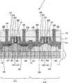
参考图26-28中的制造工艺描述使用应力施加膜来制造晶体管的传统方法。A conventional method of manufacturing a transistor using a stressor film is described with reference to the manufacturing process in FIGS. 26-28.
如图26(1)所示,在半导体衬底111上形成STI(浅沟槽隔离)结构的元件隔离区域114。As shown in FIG. 26(1), an
接着,如图26(2)所示,通过表面氧化形成氧化硅膜(未示出)作为当在硅衬底11中离子注入杂质时保护沟道的保护膜。然后,分别在n型晶体管区域和p型晶体管区域离子注入杂质,由此形成p型阱区域115和n型阱区域116。Next, as shown in FIG. 26(2), a silicon oxide film (not shown) is formed by surface oxidation as a protective film for protecting the channel when impurities are ion-implanted in the
然后,如图26(3)所示,移除保护性的氧化硅,以约1-3nm的厚度形成新的栅极氧化物膜141。Then, as shown in FIG. 26(3), the protective silicon oxide is removed, and a new
接着,如图26(4)所示,在栅极氧化物膜141上以约100-150nm的厚度形成多晶硅膜后,使用光刻技术和干法蚀刻技术,用多晶硅膜形成栅电极143和163。Next, as shown in FIG. 26(4), after forming a polysilicon film with a thickness of about 100-150 nm on the
接着,如图27(5)所示,通过杂质注入,在n型晶体管区域通过注入n型杂质(注入As离子、P离子等)形成n型延伸区域131和132,通过注入p型杂质(诸如B离子等)在p型晶体管区域形成p型延伸区域151和152。Next, as shown in FIG. 27(5), n-
接着,如图27(6)所示,在利用CVD方法和干法蚀刻方法形成包括约20nm-50nm厚度的氮化硅膜或氧化物膜的栅极侧壁绝缘膜133和153后,注入杂质离子,以形成n型晶体管区域中的源极/漏极区域135和136以及p型晶体管区域中的源极/漏极区域155和156。然后,通过瞬间在约1050℃温度下加热,活化杂质。Next, as shown in FIG. 27(6), after forming gate
接着,如图27(7)所示,按照硅化物工艺技术,使用钴(Co)、镍(Ni)等在源极/漏极区域135、136、155和156以及栅电极143和163上形成厚度为20nm-50nm的硅化物电极137、138、157、158、139和159。Next, as shown in FIG. 27 (7), according to the silicide process technology, cobalt (Co), nickel (Ni), etc. are used to form
接着,如图28(8)所示,利用CVD方法、光刻方法和干法蚀刻方法,在p型晶体管103上形成厚度为约20nm-60nm、压应力为约1GPa-3GPa的氮化硅膜的压应力线性膜122。Next, as shown in FIG. 28(8), a silicon nitride film with a thickness of about 20nm-60nm and a compressive stress of about 1GPa-3GPa is formed on the p-
此外,如图28(9)所示,利用CVD方法、光刻方法和干法蚀刻方法,在n型晶体管102上形成张应力为约1GPa-2GPa由氮化硅膜形成的张应力线性膜121。由于此线性膜的效应,压应力沿沟道的方向被施加到p型晶体管的沟道,以提高空穴的迁移率,张应力施加到n型晶体管的沟道,以提高电子的迁移率。In addition, as shown in FIG. 28 (9), a tensile stress linear film 121 formed of a silicon nitride film with a tensile stress of about 1 GPa-2 GPa is formed on the n-type transistor 102 by using the CVD method, the photolithography method, and the dry etching method. . Due to the effect of this linear film, compressive stress is applied to the channel of the p-type transistor along the direction of the channel to increase the mobility of holes, and tensile stress is applied to the channel of the n-type transistor to increase the mobility of electrons.
接着,如图28(10)所示,通过CVD方法形成由氧化硅(SiO2)等形成的层间绝缘膜171。此外,在利用干法蚀刻技术钻出接触孔后,嵌入钨(W)等金属,以形成接触电极144、145、164和165,其连接到源极/漏极区域135、136、155和156,从而完成晶体管101。Next, as shown in FIG. 28(10), an interlayer insulating film 171 made of silicon oxide (SiO2 ) or the like is formed by the CVD method. In addition, metal such as tungsten (W) is embedded to form contact electrodes 144, 145, 164, and 165, which are connected to the source/
在传统晶体管结构中,通过在完成的晶体管器件上形成应力薄膜,可以将应力施加到器件上并且比较容易地提高晶体管的迁移率;但是,存在这样的一个问题,与薄膜的应力相比,由于来自栅电极的排斥力,仅较小的应力被强加到晶体管的沟道。为了施加较大的应力,必须使得膜变厚或使得膜的内部应力自身变大。但是,当膜变厚时,存在一些问题,即,其与相邻晶体管部分开始接触,这降低了应力效应,并且因为氮化硅膜的一部分变厚而使得钻出接触孔变难。此外,当膜的内部应力变大时,存在产生膜的缺陷(诸如裂纹)的问题。In the conventional transistor structure, by forming a stressed film on the completed transistor device, stress can be applied to the device and the mobility of the transistor can be improved relatively easily; however, there is a problem that, compared with the stress of the film, due to From the repulsive force of the gate electrode, only a small stress is imposed on the channel of the transistor. In order to apply a large stress, it is necessary to make the film thick or make the internal stress of the film itself large. However, when the film becomes thick, there are problems that it comes into contact with adjacent transistor parts, which reduces the stress effect, and makes it difficult to drill a contact hole because a part of the silicon nitride film becomes thick. In addition, when the internal stress of the film becomes large, there is a problem that defects of the film such as cracks are generated.
要解决的问题是,在在晶体管器件上形成具有应力的薄膜结构中,与薄膜的应力相比,由于来自栅电极的排斥力,仅较小的应力被施加到晶体管的沟道上。The problem to be solved is that in forming a thin film structure with stress on a transistor device, only a small stress is applied to the channel of the transistor due to the repulsive force from the gate electrode compared to the stress of the film.
本发明的目的在于通过提高施加在晶体管沟道区域的应力而增强电流提高效应。The object of the present invention is to enhance the current enhancing effect by increasing the stress applied to the channel region of the transistor.
发明内容Contents of the invention
根据权利要求1的本发明的特征在于包括:侧壁绝缘膜,其形成在半导体衬底上,具有通过移除牺牲栅极而形成的沟槽;栅电极,其经由栅极绝缘膜而形成于所述半导体衬底上的所述沟槽内;应力施加膜,其沿所述侧壁绝缘膜形成于所述半导体衬底上方;以及源极/漏极区域,其在所述半导体衬底中形成于所述栅电极的两侧,其特征还在于:所述应力施加膜在形成所述沟槽之前形成。The invention according to
在根据权利要求1的发明中,因为应力施加膜在形成所述沟槽之前形成,所述牺牲栅极是在以下状态下移除的:由于所述应力施加膜而有应力施加在所述半导体衬底上。因此,已经施加到所述牺牲栅极上的应力开始施加到半导体衬底上移除所述牺牲栅极的区域,即,晶体管沟道区域,由此提高施加到所述沟道区域的应力。In the invention according to
根据权利要求5的本发明包括n型晶体管和p型晶体管,其特征在于:所述n型晶体管在所述半导体衬底的n型晶体管形成区域中具有:侧壁绝缘膜,其形成在所述半导体衬底上,具有通过移除第一牺牲栅极而形成的第一沟槽;栅电极,其经由栅极绝缘膜在所述半导体衬底上形成于所述第一沟槽内;具有张应力的第一应力施加膜,沿所述侧壁绝缘膜形成于所述半导体衬底上方;以及源极/漏极区域,其在所述半导体衬底中形成于所述栅电极的两侧;并且所述p型晶体管在所述半导体衬底的p型晶体管形成区域中,具有:侧壁绝缘膜,其形成在所述半导体衬底上,具有通过移除第二牺牲栅极而形成的第二沟槽;栅电极,其在所述半导体衬底上经由栅极绝缘膜形成于所述第二沟槽内;具有压应力的第二应力施加膜,其沿所述侧壁绝缘膜形成于所述半导体衬底上方,以及源极/漏极区域,其在所述半导体衬底中形成于所述栅电极的两侧,其特征还在于:所述第一应力施加膜在形成所述第一沟槽之前形成;所述第二应力施加膜在形成所述第二沟槽之前形成。The present invention according to
在根据权利要求5的发明中,因为所述第一应力施加膜在形成所述第一沟槽之前形成并且所述第二应力施加膜在形成所述第二沟槽之前形成,所以在应力由于所述应力施加膜而已施加在所述半导体衬底的状态下移除所述牺牲栅极。因此,已经施加到所述牺牲栅极上的应力开始施加到半导体衬底上移除所述牺牲栅极的区域,即,晶体管沟道区域,由此提高施加到所述沟道区域的应力。In the invention according to
根据权利要求17的发明的特征在于包括:在半导体衬底上形成牺牲栅极、接着在所述牺牲栅极的每个侧壁上形成侧壁绝缘膜以及在所述半导体衬底中在各个所述牺牲栅极的两侧形成源极/漏极区域的步骤;沿所述侧壁绝缘膜而在所述半导体衬底上方形成应力施加膜的步骤;通过移除所述牺牲栅极形成沟槽的步骤;以及经由栅极绝缘膜而在所述半导体衬底上所述沟槽内形成栅电极的步骤。The invention according to claim 17 is characterized by comprising: forming a sacrificial gate on a semiconductor substrate, followed by forming a sidewall insulating film on each side wall of the sacrificial gate, and forming each of the sacrificial gates in the semiconductor substrate A step of forming source/drain regions on both sides of the sacrificial gate; a step of forming a stress application film above the semiconductor substrate along the sidewall insulating film; forming a trench by removing the sacrificial gate and a step of forming a gate electrode in the trench on the semiconductor substrate via a gate insulating film.
在根据权利要求17的发明中,因为应力施加膜在形成所述沟槽之前形成,所以在应力由于所述应力施加膜而已施加在所述半导体衬底的状态下移除所述牺牲栅极。因此,已经施加到所述牺牲栅极上的应力开始施加到半导体衬底上移除所述牺牲栅极的区域,即,晶体管沟道区域,由此提高施加到所述沟道区域的应力。In the invention according to claim 17, since the stress applying film is formed before forming the trench, the sacrificial gate is removed in a state where stress has been applied to the semiconductor substrate due to the stress applying film. Accordingly, the stress already applied to the sacrificial gate starts to be applied to the region of the semiconductor substrate from which the sacrificial gate was removed, ie, the transistor channel region, thereby increasing the stress applied to the channel region.
在根据权利要求19的发明中,提供了一种制造半导体器件的方法,其特征在于包括:在半导体衬底上在n型晶体管形成区域和p型晶体管形成区域中均形成牺牲栅极、接着在各个所述牺牲栅极的侧壁上形成侧壁绝缘膜以及在所述半导体衬底中在各个所述牺牲栅极的两侧形成源极/漏极区域的步骤;沿所述侧壁绝缘膜而在所述半导体衬底上方的所述n型晶体管形成区域中形成第一应力施加膜的步骤;沿所述侧壁绝缘膜而在所述半导体衬底上方的所述p型晶体管形成区域中形成第二应力施加膜的步骤;通过移除各个所述牺牲栅极形成沟槽的步骤;以及经由栅极绝缘膜而在所述半导体衬底上的各个所述沟槽内形成栅电极的步骤。In the invention according to claim 19, there is provided a method of manufacturing a semiconductor device characterized by comprising: forming a sacrificial gate in both an n-type transistor formation region and a p-type transistor formation region on a semiconductor substrate, followed by a step of forming a sidewall insulating film on the sidewall of each of the sacrificial gates and forming a source/drain region on both sides of each of the sacrificial gates in the semiconductor substrate; and a step of forming a first stress applying film in the n-type transistor formation region above the semiconductor substrate; in the p-type transistor formation region above the semiconductor substrate along the side wall insulating film a step of forming a second stress applying film; a step of forming a trench by removing each of the sacrificial gates; and a step of forming a gate electrode in each of the trenches on the semiconductor substrate via a gate insulating film .
在根据权利要求19的发明中,因为所述第一应力施加膜在形成所述第一沟槽之前形成并且所述第二应力施加膜在形成所述第二沟槽之前形成,所以在应力由于所述应力施加膜而已经施加在所述半导体衬底的状态下移除所述牺牲栅极。因此,已经施加到所述牺牲栅极上的应力开始施加到半导体衬底上移除所述牺牲栅极的区域,即,晶体管沟道区域,由此提高施加到所述沟道区域的应力。In the invention according to claim 19, since the first stress applying film is formed before forming the first groove and the second stress applying film is formed before forming the second groove, when the stress due to The sacrificial gate is removed in a state where the stress applying film has been applied to the semiconductor substrate. Accordingly, the stress already applied to the sacrificial gate starts to be applied to the region of the semiconductor substrate from which the sacrificial gate was removed, ie, the transistor channel region, thereby increasing the stress applied to the channel region.
根据本发明,因为施加到晶体管的沟道区域的应力增大,所以可以急剧增大迁移率,由此有利地提高晶体管的响应性能。According to the present invention, since the stress applied to the channel region of the transistor increases, the mobility can be sharply increased, thereby advantageously improving the response performance of the transistor.
附图说明Description of drawings
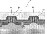
图1是示出根据本发明的半导体器件的一个实施例(第一实施例)的示意性剖面结构视图。FIG. 1 is a schematic sectional structural view showing one embodiment (first embodiment) of a semiconductor device according to the present invention.
图2是示出根据本发明的制造半导体器件的方法的一个实施例(第一实施例)的制造工艺的剖面图。2 is a sectional view showing a manufacturing process of one embodiment (first embodiment) of the method of manufacturing a semiconductor device according to the present invention.
图3是示出根据本发明的制造半导体器件的方法的一个实施例(第一实施例)的制造工艺的剖面图。3 is a sectional view showing a manufacturing process of one embodiment (first embodiment) of the method of manufacturing a semiconductor device according to the present invention.
图4是示出根据本发明的制造半导体器件的方法的一个实施例(第一实施例)的制造工艺的剖面图。4 is a sectional view showing a manufacturing process of one embodiment (first embodiment) of the method of manufacturing a semiconductor device according to the present invention.
图5是示出根据本发明的制造半导体器件的方法的一个实施例(第一实施例)的制造工艺的剖面图。5 is a sectional view showing a manufacturing process of one embodiment (first embodiment) of the method of manufacturing a semiconductor device according to the present invention.
图6是示出根据本发明的制造半导体器件的方法的一个实施例(第一实施例)的制造工艺的剖面图。6 is a sectional view showing a manufacturing process of one embodiment (first embodiment) of the method of manufacturing a semiconductor device according to the present invention.
图7是示出根据本发明的制造半导体器件的方法的一个实施例(第一实施例)的制造工艺的剖面图。7 is a sectional view showing a manufacturing process of one embodiment (first embodiment) of the method of manufacturing a semiconductor device according to the present invention.
图8是用于描述根据第一实施例的n型晶体管的应力增加效应的示意图。FIG. 8 is a schematic diagram for describing the stress increase effect of the n-type transistor according to the first embodiment.
图9是用于描述根据第一实施例的p型晶体管的应力增加效应的示意图。FIG. 9 is a schematic diagram for describing the stress increase effect of the p-type transistor according to the first embodiment.
图10是用于描述根据第一实施例的n型和p型晶体管的迁移率增强效应的示意图。FIG. 10 is a schematic diagram for describing the mobility enhancement effect of n-type and p-type transistors according to the first embodiment.
图11是示出根据本发明的半导体器件的另一个实施例(第二实施例)的示意性剖面结构视图。11 is a schematic cross-sectional structural view showing another embodiment (second embodiment) of the semiconductor device according to the present invention.
图12是示出根据本发明的制造半导体器件的方法的实施例(第二实施例)的制造工艺的剖面图。12 is a sectional view showing a manufacturing process of the embodiment (second embodiment) of the method of manufacturing a semiconductor device according to the present invention.
图13是示出根据本发明的制造半导体器件的方法的实施例(第二实施例)的制造工艺的剖面图。13 is a sectional view showing a manufacturing process of the embodiment (second embodiment) of the method of manufacturing a semiconductor device according to the present invention.
图14是用于描述根据第二实施例的n型晶体管的应力增加效应的示意图。FIG. 14 is a schematic diagram for describing the stress increase effect of the n-type transistor according to the second embodiment.
图15是用于描述根据第二实施例的p型晶体管的应力增加效应的示意图。FIG. 15 is a schematic diagram for describing the stress increase effect of the p-type transistor according to the second embodiment.
图16是用于描述根据第二实施例的n型和p型晶体管的迁移率增强效应的示意图。FIG. 16 is a schematic diagram for describing the mobility enhancement effect of n-type and p-type transistors according to the second embodiment.
图17是示出根据本发明的半导体器件的另一个实施例(第三实施例)的示意性剖面结构视图。17 is a schematic cross-sectional structural view showing another embodiment (third embodiment) of the semiconductor device according to the present invention.
图18是示出根据本发明的半导体器件的另一个实施例(第四实施例)的示意性剖面结构视图。18 is a schematic cross-sectional structural view showing another embodiment (fourth embodiment) of the semiconductor device according to the present invention.
图19是用于描述根据第三和第四实施例的p型晶体管的应力增加效应的示意图。FIG. 19 is a schematic diagram for describing the stress increase effect of the p-type transistors according to the third and fourth embodiments.
图20是用于描述根据第三和第四实施例的p型晶体管的迁移率增强效应的示意图。FIG. 20 is a schematic diagram for describing the mobility enhancement effect of the p-type transistor according to the third and fourth embodiments.
图21是示出根据本发明的半导体器件的另一个实施例(第五实施例)的示意性剖面结构视图。21 is a schematic cross-sectional structural view showing another embodiment (fifth embodiment) of the semiconductor device according to the present invention.
图22是示出根据本发明的半导体器件的另一个实施例(第六实施例)的示意性剖面结构视图。FIG. 22 is a schematic sectional structural view showing another embodiment (sixth embodiment) of the semiconductor device according to the present invention.
图23是用于描述根据第五和第六实施例的p型晶体管的应力增加效应的示意图。FIG. 23 is a schematic diagram for describing the stress increase effect of the p-type transistors according to the fifth and sixth embodiments.
图24是用于描述根据第五和第六实施例的p型晶体管的迁移率增强效应的示意图。FIG. 24 is a schematic diagram for describing the mobility enhancement effect of the p-type transistor according to the fifth and sixth embodiments.
图25是示出根据本发明的半导体器件的另一个实施例(第七实施例)的示意性剖面结构视图。25 is a schematic cross-sectional structural view showing another embodiment (seventh embodiment) of the semiconductor device according to the present invention.
图26是示出根据传统技术的制造半导体器件的方法的一个示例的制造工艺的剖面图。FIG. 26 is a cross-sectional view illustrating a manufacturing process of one example of a method of manufacturing a semiconductor device according to the conventional art.
图27是示出根据传统技术的制造半导体器件的方法的示例的制造工艺的剖面图。27 is a cross-sectional view illustrating a manufacturing process of an example of a method of manufacturing a semiconductor device according to a conventional art.
图28是示出根据传统技术的制造半导体器件的方法的示例的制造工艺的剖面图。28 is a sectional view illustrating a manufacturing process of an example of a method of manufacturing a semiconductor device according to a conventional art.
具体实施方式Detailed ways
参考图1的示意性剖面结构视图,描述根据本发明的半导体器件的一个实施例(第一实施例)。One embodiment (first embodiment) of the semiconductor device according to the present invention will be described with reference to the schematic sectional structural view of FIG. 1 .
如图1所示,在半导体衬底11上形成分别隔开n型晶体管形成区域12和p型晶体管形成区域13的元件隔离区域14。例如,硅衬底用作半导体衬底11,并且例如元件隔离区域14形成在包括氧化物膜的STI(浅沟槽隔离)结构中。As shown in FIG. 1 ,
具有p型杂质引入的p型阱区域15形成在半导体衬底11的n型晶体管形成区域12中,具有n型杂质引入的n型阱区域16形成在半导体衬底11的p型晶体管形成区域13中。A p-
在半导体衬底11上,具有通过移除第一牺牲栅极(未示出)而形成的第一沟槽39的侧壁绝缘膜33形成在n型晶体管形成区域12中,而具有通过移除第二牺牲栅极(未示出)而形成的第二沟槽59的侧壁绝缘膜53形成在p型晶体管形成区域13中。侧壁绝缘膜33和53的厚度例如形成为约20nm-50nm。On the
栅电极43经由栅极绝缘膜41而形成于半导体衬底11上的第一沟槽39内,栅电极63经由栅极绝缘膜41而形成于半导体衬底11上的第二沟槽59内。The
例如,栅极绝缘膜41由氧化铪(HfO2)膜、高介电常数(高k)的绝缘膜形成,其厚度为约2nm-3nm。虽然此实施例采用HfO2,但是可以使用另外的高k材料,诸如HfSiO、氧化钽(Ta2O5)、氧化铝铪(HfAlOx)等,或者,半导体材料的表面(例如,硅表面)可以简单地被氧化作为栅极绝缘膜41。或者,高介电常数(高k)绝缘膜可以预先形成于半导体衬底11的表面上并且可以作为栅极绝缘膜。For example, the
例如,栅电极43和63由金属化合物层或金属层形成。作为示例,这里使用氮化钛(TiN)。作为金属层,可以选择钨(W)、钛(Ti)、氮化钛(TiN)、铪(Hf)、硅化铪(HfSi)、钌(Ru)、铱(Ir)、钴(Co)等。虽然本实施例采用单层,但是可以层叠多层金属膜,以降低阻抗和调节阈值电压。For example, the
延伸区域31和32在半导体衬底11中形成于n型晶体管形成区域12中的第一沟槽39的两侧。此外,源极/漏极区域35和36在半导体衬底11中经由各个延伸区域31和32形成于第一沟槽39的两侧。作为n型杂质,磷(P)或砷(As)被引入到延伸区域31和32以及源极/漏极区域35和36。The
此外,在p型晶体管形成区域13中,延伸区域51和52在半导体衬底11中形成于第二沟槽59的两侧。此外,源极/漏极区域55和56经由各个延伸区域51和52在半导体衬底11中形成于第二沟槽59的两侧。作为p型杂质,硼(B)、铟(In)等被引入到延伸区域51和52以及源极/漏极区域55和56中。Furthermore, in the p-type
硅化物电极37和38形成在源极/漏极区域35和36上,硅化物电极57和58形成在源极/漏极区域55和56上,由此降低各个源极/漏极区域的阻抗。各个硅化物电极37、38、57和58由例如含钴(Co)、镍(Ni)、铂(Pt)或其化合物的硅化物层形成,其厚度为20nm-30nm。
在n型晶体管形成区域12中,具有张应力的第一应力施加膜21沿着侧壁绝缘膜33形成在半导体衬底11上,在p型晶体管形成区域13中,具有压应力的第二应力施加膜22沿着侧壁绝缘膜53形成在半导体衬底11上。这样,在形成第一沟槽39之前形成第一应力施加膜21,在形成第二沟槽59之前形成第二应力施加膜22。In the n-type
例如第一应力施加膜21由具有张应力的氮化硅膜形成,膜厚度为约40nm。虽然在本实施例中形成具有约1.2GPa的张应力的膜,但是应力并不局限于此值。膜厚度并不局限于本实施例中的上述膜厚度。For example, the first
此外,例如第二应力施加膜22由具有压应力的氮化硅膜形成,膜厚度为约40nm。虽然在本实施例中形成具有约1.2GPa的压应力的膜,但是应力并不局限于此值。膜厚度并不局限于本实施例中的上述膜厚度。In addition, for example, the second
此外,第一层间绝缘膜71和第二层间绝缘膜72形成在半导体衬底11的整个表面上。例如,这些第一和第二层间绝缘膜71和72由氧化硅(SiO2)膜形成。Furthermore, a first
与源极/漏极区域35、36、55和56连通的接触空73、74、75和76形成于第二层间绝缘膜72和第一层间绝缘膜71中,形成嵌入钨(W)等的源/漏电极44、45、64和65。这样就构造成包括n型晶体管Tr1和p型晶体管Tr2的半导体器件1。Contact holes 73, 74, 75, and 76 communicating with the source/
接着,参考图2-7中的制造工艺的剖视图描述制造半导体衬底的制造方法的实施例(第一实施例)。这里,描述根据第一实施例的制造半导体器件的方法。Next, an embodiment (first embodiment) of a manufacturing method for manufacturing a semiconductor substrate is described with reference to sectional views of the manufacturing process in FIGS. 2-7. Here, a method of manufacturing a semiconductor device according to the first embodiment is described.
如图2(1)所示,电隔离n型晶体管形成区域12和p型晶体管形成区域13的元件隔离区域14形成于半导体衬底11上。例如,上述半导体衬底11采用硅衬底,并且元件隔离区域14形成在例如由氧化物膜形成的STI(浅沟槽隔离)结构中。As shown in FIG. 2(1), an
接着,如图2(2)所示,用于在离子注入时保护沟道的保护膜80形成在半导体衬底11上。例如,保护膜80由氧化硅膜形成,其厚度为约5nm-10nm。例如,其形成方法采用表面氧化。接着,在形成覆盖p型晶体管形成区域13的离子注入掩膜(未示出)之后,按照离子注入方法,在半导体衬底11的n型晶体管形成区域12中引入p型杂质,以形成p型阱区域15。Next, as shown in FIG. 2(2), a
此后,移除上述离子注入掩膜。Thereafter, the above ion implantation mask is removed.
接着,在形成覆盖n型晶体管形成区域12的离子注入掩膜(未示出)之后,按照离子注入方法,在半导体衬底11的p型晶体管形成区域13中引入n型杂质,以形成n型阱区域16。Next, after forming an ion implantation mask (not shown) covering the n-type
此后,移除上述离子注入掩膜。此外,移除保护膜18。Thereafter, the above ion implantation mask is removed. Furthermore, the protective film 18 is removed.
可以首先形成p型阱区域15和n型阱区域16中的任何一个。Either one of p-
接着,如图2(3)所示,在半导体衬底11上顺序地形成牺牲栅极绝缘膜81、牺牲栅极形成膜82和硬掩膜层83。Next, as shown in FIG. 2(3), a sacrificial
例如,牺牲栅极绝缘膜81由氧化硅膜形成,其厚度为约1nm-3nm。例如,形成膜的方法采用热氧化工艺。For example, sacrificial
例如,牺牲栅极形成膜82由多晶硅膜形成,其厚度为约100nm-150nm。其形成方法例如采用CVD方法等。虽然,在本实施例的后续工艺中移除牺牲栅极绝缘膜,但是,在某些情况下可以在此阶段形成栅极绝缘膜。例如,栅极绝缘膜可以使用氧化铪(HfO2)等的高介电常数(高k)绝缘膜。牺牲栅极形成膜82可以采用无定形硅膜。For example, sacrificial
硬掩膜83例如使用氮化硅膜,其厚度为约30nm-100nm。膜形成方法例如采用CVD方法。For the
然后,在硬掩膜层83上通过光刻技术或电子束光刻技术图案化光刻胶(未示出),以形成用于形成晶体管的栅电极的光刻胶掩膜图案(未示出)。使用光刻胶掩膜图案作为掩膜,通过干法蚀刻方法等蚀刻硬掩膜层83。在蚀刻之后,移除光刻胶掩膜图案,在剩余的硬掩膜层83作为蚀刻掩膜的情况下,使用干法蚀刻方法等蚀刻牺牲栅极形成膜82和牺牲栅极绝缘膜81。Then, a photoresist (not shown) is patterned on the
由此,如图3(4)所示,在半导体衬底11上形成牺牲栅极84和85。Thus,
优选地,在几乎不导致蚀刻硬掩膜层83的选择比的情况下进行干法蚀刻。Preferably, dry etching is performed with little resulting in a selectivity of etching the
接着,如图3(5)所示,在n型晶体管形成区域12中,延伸区域31和32在半导体衬底11中形成于n型晶体管形成区域12中的牺牲栅极84的两侧。Next, as shown in FIG. 3(5), in n-type
在p型晶体管形成区域13中,延伸区域51和52在半导体衬底11中形成于p型晶体管形成区域13中的牺牲栅极85的两侧。In the p-type
更具体而言,在形成覆盖p型晶体管形成区域13的离子注入掩膜(未示出)之后,根据离子注入方法,在半导体衬底11的n型晶体管形成区域12中的牺牲栅极84的两侧引入n型杂质,由此形成延伸区域31和32。在此离子注入中,例如使用磷(P)、砷(As)等作为n型杂质。此外,例如,使用光刻胶膜作为n型杂质的离子注入掩膜。此后,移除上述离子注入掩膜。More specifically, after forming an ion implantation mask (not shown) covering the p-type
然后,在形成覆盖n型晶体管形成区域12的离子注入掩膜(未示出)之后,根据离子注入方法,在半导体衬底11的p型晶体管形成区域13中的牺牲栅极85的两侧引入p型杂质,由此形成延伸区域51和52。在此离子注入中,例如使用硼(B)、铟(In)等作为p型杂质。此外,例如,使用光刻胶膜作为p型杂质的离子注入掩膜。Then, after forming an ion implantation mask (not shown) covering the n-type
此后,移除离子注入掩膜。Thereafter, the ion implantation mask is removed.
在各个延伸区域31、32、51和52中注入杂质之前,可以由侧壁保护膜(诸如氮化硅膜、氧化硅膜等)保护各个牺牲栅极84和85的侧壁。Before impurity is implanted in the
接着,如图3(6)所示,在牺牲栅极84和85的各个侧壁上分别形成侧壁绝缘膜33和53。侧壁绝缘膜33和53的厚度例如形成为约20nm-50nm。Next, as shown in FIG. 3(6), side
此后,源极/漏极区域35和36经由各个延伸区域31和32而在半导体衬底11中形成于牺牲栅极84的两侧。Thereafter, source/
同样,源极/漏极区域55和56经由各个延伸区域51和52而在半导体衬底11中形成于牺牲栅极85的两侧。Also, source/
在p型晶体管形成区域中形成离子注入掩膜(未示出)之后,例如在半导体衬底11中通过离子注入n型杂质形成源极/漏极区域35和36。After forming an ion implantation mask (not shown) in the p-type transistor formation region, source/
接着,移除上述离子注入掩膜。Next, the above-mentioned ion implantation mask is removed.
此外,在n型晶体管形成区域中形成离子注入掩膜(未示出)之后,例如在半导体衬底11中通过离子注入p型杂质形成源极/漏极区域55和56。Further, source/
接着,移除上述离子注入掩膜。Next, the above-mentioned ion implantation mask is removed.
此后,进行活化退火,以活化延伸区域31、32、51和52以及源极/漏极区域35、36、55和56中所注入的杂质。例如通过在约1000℃-1100℃下快速热退火(RTA)进行活化退火。Thereafter, activation annealing is performed to activate the implanted impurities in the
接着,如图4(7)所示,根据硅化物工艺技术,硅化物电极37和38形成在源极/漏极区域35和36上,硅化物电极57和58形成在源极/漏极区域55和56上,由此降低各个源极/漏极区域的阻抗。在硅化物工艺技术中,厚度为约20nm-50nm的硅化物层由钴(Co)、镍(Ni)、铂(Pt)或其化合物形成。Next, as shown in FIG. 4 (7), according to the silicide process technology,
接着,如图4(8)所示,具有压应力的第二应力施加膜(压应力线性膜)22形成在整个表面上。此应力施加膜按照等离子体CVD方法由具有1.2GPa的压应力的氮化硅膜形成,其膜厚度为40nm。Next, as shown in FIG. 4(8), a second stress applying film (compressive stress linear film) 22 having compressive stress is formed on the entire surface. This stress applying film is formed of a silicon nitride film having a compressive stress of 1.2 GPa in accordance with the plasma CVD method, and its film thickness is 40 nm.
通过在400℃-600℃的衬底温度、0.13kPa-0.67kPa的压力以及50W-500W的RF功率条件下,提供用于化学反应的氢气(H2)(1000cm3/min-5000cm3/min)、氮气(N2)(500cm3/min-2500cm3/min)、氩气(Ar)(1000cm3/min-5000cm3/min)、氨气(NH3)(50cm3/min-200cm3/min)以及三甲基硅烷气体(10cm3/min-50cm3/min),形成第二应力施加膜22。Provide hydrogen (H2 ) (1000cm3 /min-5000cm3 /min ), nitrogen (N2 ) (500cm3 /min-2500cm3 /min), argon (Ar) (1000cm3 /min-5000cm3 /min), ammonia (NH3 ) (50cm3 /min-200cm3 /min) and trimethylsilane gas (10cm3 /min-50cm3 /min) to form the second
虽然在本实施例中形成具有约1.2GPa的压应力的膜,但是应力并不局限于此值。同样,膜厚度也并不局限于本实施例中的上述膜厚度。Although a film having a compressive stress of about 1.2 GPa was formed in this embodiment, the stress is not limited to this value. Also, the film thickness is not limited to the above-mentioned film thickness in this embodiment.
此后,将光刻技术和干法蚀刻技术用于处理第二应力施加膜22,使得仅在p型晶体管形成区域13上的第二应力施加膜22保留下来。Thereafter, a photolithography technique and a dry etching technique are used to process the second
接着,如图4(9)所示,具有张应力的第一应力施加膜(张应力线性膜)21形成在整个表面上。此第一应力施加膜21按照等离子体CVD方法由具有1.2GPa的张应力的氮化硅膜形成,其膜厚度为40nm。Next, as shown in FIG. 4(9), a first stress applying film (tensile stress linear film) 21 having a tensile stress is formed on the entire surface. This first
通过在200℃-400℃的衬底温度、0.67kPa-2.0kPa的压力以及50W-500W的RF功率条件下,提供用于化学反应的氮气(N2)(500cm3/min-2000cm3/min)、氨气(NH3)(500cm3/min-1500cm3/min)、硅烷(SiH4)气体(50cm3/min-300cm3/min),形成第一应力施加膜21。此外,在膜形成之后,在400℃-600℃的温度、0.67kPa-2.0kPa的压力下以及1kW-10kW紫外线(UV)灯功率的条件下,供应氦气(He)(10L/min-20L/min)并进行紫外照射处理。Nitrogen (N2 ) (500cm3 /min-2000cm3 /min ), ammonia gas (NH3 ) (500cm3 /min-1500cm3 /min), silane (SiH4 ) gas (50cm3 /min-300cm3 /min), to form the first
虽然在本实施例中形成具有约1.2GPa的张应力的膜,但是应力并不局限于此值。此外,膜厚度不并局限于本实施例中的上述膜厚度。Although a film having a tensile stress of about 1.2 GPa was formed in this embodiment, the stress is not limited to this value. In addition, the film thickness is not limited to the above-mentioned film thickness in this embodiment.
此后,将光刻技术和干法蚀刻技术用于处理第一应力施加膜21,使得仅在n型晶体管形成区域12上的第一应力施加膜21保留下来。可以首先形成第一和第二应力施加膜21和22中的任何一个。Thereafter, a photolithography technique and a dry etching technique are used to process the first
接着,如图5(10)所示,第一层间绝缘膜71形成在半导体衬底11的整个表面上。第一层间绝缘膜71例如由氧化硅(SiO2)膜形成。Next, as shown in FIG. 5(10), a first
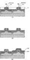
接着,如图5(11)所示,移除第一层间绝缘膜71的表面部分,以暴露各个牺牲栅极84和85的顶部。在此移除工艺中,例如按照CMP方法抛光第一层间绝缘膜71的表面。然后,暴露各个牺牲栅极84和85的顶部。Next, as shown in FIG. 5(11), the surface portion of the first
接着,如图5(12)所示,移除牺牲栅极84和85(参考图5(11))。此移除工艺通过干法蚀刻进行。继续地,通过湿法蚀刻使用氢氟酸移除牺牲栅极绝缘膜81的氧化硅膜,以形成沟槽39和59。由此,在侧壁绝缘膜33和53内形成沟槽39和59。Next, as shown in FIG. 5(12), the
接着,如图6(13)所示,栅极绝缘膜41形成在包括沟槽39和49的内表面在内的第一层间绝缘膜71的表面上。例如,栅极绝缘膜41按照CVD方法等由氧化铪(HfO2)膜、高介电常数(高k)的绝缘膜形成,其厚度为约2nm-3nm。虽然此实施例采用HfO2,但是可以使用其它高k材料,诸如HfSiO、氧化钽(Ta2O5)、氧化铝铪(HfAlOx)等,或者,半导体衬底11的表面(例如,硅表面)可以简单地被氧化作为栅极绝缘膜41。或者,高介电常数(高k)绝缘膜可以预先形成于半导体衬底11的表面上并且可以作为栅极绝缘膜。Next, as shown in FIG. 6(13), a
如图6(14)所示,栅电极形成层42经由栅极绝缘膜41而嵌入在沟槽39和59中。此栅电极形成层42例如使用金属化合物层或金属层。这里,作为示例,使用氮化钛(TiN)。形成栅电极形成层42的方法例如采用ALD方法(原子层沉积)或PVD方法(物理气相沉积)。本实施例通过PVD方法采用具有压应力的氮化钛(TiN)膜。作为金属层,可以选择钨(W)、钛(Ti)、氮化钛(TiN)、铪(Hf)、硅化铪(HfSi)、钌(Ru)、铱(Ir)、钴(Co)等。虽然本实施例采用单层膜,但是可以层叠多层金属膜,以降低阻抗和调节阈值电压。As shown in FIG. 6 ( 14 ), the gate
如图6(15)所示,移除第一层间绝缘膜71上的剩余栅电极形成膜42和栅极绝缘膜41,使得栅电极形成层42嵌入在沟槽39和59中,由此形成栅电极43和63。此移除工艺例如采用CMP,其中,抛光上层使得暴露第一层间绝缘膜71的表面。As shown in FIG. 6 (15), the remaining gate electrode-forming
接着,如图7(16)所示,第二层间绝缘膜72形成在第一层间绝缘膜71上。第二层间绝缘膜72例如由氧化硅(SiO2)膜形成。使用干法蚀刻技术在第二层间绝缘膜72和第一层间绝缘膜71中钻出与源极/漏极区域35、36、55和56连通的接触孔73、74、75和76之后,嵌入包括钨(W)等的金属,以形成源/漏电极44、45、64和65,由此完成了包括n型晶体管Tr1和p型晶体管Tr2的半导体器件1。Next, as shown in FIG. 7(16), a second
接着,参考图8-10描述上述第一实施例中的应力增加效应。图8-10示出根据上述第一实施例的结构形成的应力模拟结果。Next, the stress increasing effect in the first embodiment described above will be described with reference to FIGS. 8-10. 8-10 show stress simulation results for the formation of the structure according to the first embodiment described above.
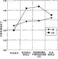
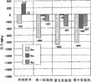
图8示出传统技术和本发明第一实施例的各个工艺的n型晶体管的沟道中的应力。此模拟假设栅极长度为60nm。另外,在此模拟中,x轴限定为从源极到漏极的方向(晶体管栅极长度(L)的方向),y轴限定为从栅电极开始的衬底深度方向,z轴限定为从前方向后方的方向(晶体管栅极宽度(W)的方向),标号Sxx、Syy和Szz表示朝向各个方向的主应力分量。沟道中的应力表示在栅极的中间部分从硅衬底的表面到深度1nm处的值。在图8-10中,“传统技术”示出图28(10)状态下的应力值,“移除牺牲栅极后”示出根据实施例刚移除牺牲栅极后的应力值;“移除牺牲栅极和牺牲氧化物膜之后”示出根据实施例刚移除牺牲栅极和牺牲栅极绝缘层(图5(12))后的应力值;以及“形成栅电极后”示出刚形成栅电极43和63(图6(15))后的应力值,并且在每种情况下,示出Sxx、Syy和Szz的值。正(+)应力值表示张应力,负(-)应力值表示压应力。FIG. 8 shows the stress in the channel of the n-type transistor of the respective processes of the conventional technology and the first embodiment of the present invention. This simulation assumes a gate length of 60nm. Also, in this simulation, the x-axis is defined as the direction from the source to the drain (the direction of the transistor gate length (L)), the y-axis is defined as the substrate depth direction from the gate electrode, and the z-axis is defined as the direction from the front In the direction of the rear direction (the direction of the gate width (W) of the transistor), the symbols Sxx, Syy, and Szz denote principal stress components toward the respective directions. The stress in the channel represents a value at a depth of 1 nm from the surface of the silicon substrate at the middle portion of the gate. In FIGS. 8-10 , “conventional technology” shows the stress value in the state of FIG. After removing the sacrificial gate and the sacrificial oxide film" shows the stress value just after removing the sacrificial gate and the sacrificial gate insulating layer ( FIG. 5 ( 12 )) according to the embodiment; Stress values after forming the
根据上述模拟结果,发现与传统技术相比,Sxx的值在刚移除牺牲栅极后急剧增大。这说明,在传统技术中,由于来自栅电极的排出功率,从受压(应力线性)膜施加的应力没有有效地施加到半导体衬底(硅衬底)上,但是在移除多晶硅牺牲栅极后张应力有效地沿x方向施加。但是发现,在传统技术中,压应力作为Syy施加,而其在刚移除牺牲栅极之后消失。此外,相对于Szz,在传统技术中只发现极小的应力,但是在移除牺牲栅极后施加张应力。此外,在移除牺牲栅极绝缘膜后,发现Sxx通过移除牺牲栅极绝缘膜而进一步增大。应力的趋势不发生变化,即使在形成栅电极43和63之后。According to the above simulation results, it is found that the value of Sxx increases sharply just after removing the sacrificial gate compared with the conventional technology. This shows that in the conventional technology, the stress applied from the stressed (stress linear) film is not effectively applied to the semiconductor substrate (silicon substrate) due to the draining power from the gate electrode, but after removing the polysilicon sacrificial gate Post-tensile stress is effectively applied in the x-direction. However, it was found that in the conventional technique, compressive stress was applied as Syy, which disappeared just after the sacrificial gate was removed. Furthermore, relative to Szz, only minimal stress is found in conventional techniques, but tensile stress is applied after removal of the sacrificial gate. Furthermore, after removing the sacrificial gate insulating film, it was found that Sxx was further increased by removing the sacrificial gate insulating film. The tendency of the stress does not change even after the
图9示出p型晶体管的应力变化。因为p型晶体管使用具有压应力的受应力(应力线性)膜,与n型晶体管相反,正/负应力值颠倒,但是与在n型晶体管的情况下趋势是相同的。即,通过移除牺牲栅极,Sxx和Szz值增加,但是Syy值减小。此外发现,即使在形成栅电极43和63之后,值仍具有相同的趋势。FIG. 9 shows the stress variation of a p-type transistor. Since p-type transistors use a stressed (stress-linear) film with compressive stress, contrary to n-type transistors, positive/negative stress values are reversed, but the tendency is the same as in the case of n-type transistors. That is, by removing the sacrificial gate, the Sxx and Szz values increase, but the Syy value decreases. Furthermore, it was found that the values had the same tendency even after the
作为估计根据这些应力值的迁移率的变化的方法,已知使用压阻系数的方法。根据在C.S.Smith所著的Phys.Rev.vo.94,pp42-49(1954)中所公开的压阻系数,n型和p型晶体管中的每种迁移率增强因子如下所述。As a method of estimating changes in mobility according to these stress values, a method using a piezoresistive coefficient is known. According to the piezoresistive coefficient disclosed in Phys. Rev. vo. 94 by C.S. Smith, pp42-49 (1954), each mobility enhancement factor in n-type and p-type transistors is as follows.
N型:(μxx/μ0)=1+0.316Sxx-0.534Syy+0.176SzzType N: (μxx/μ0)=1+0.316Sxx-0.534Syy+0.176Szz
P型:(μxx/μ0)=1-0.718Sxx+0.011Syy+0.663SzzP type: (μxx/μ0)=1-0.718Sxx+0.011Syy+0.663Szz
图10中示出根据上述公式在各个状态下的每种迁移率增强因子的图。图8和9中示出了用于计算的Sxx、Syy和Szz值。迁移率增强因子是当没有施加应力的状态下的迁移率被定义为1时的相对值。A graph of each mobility enhancement factor in each state according to the above formula is shown in FIG. 10 . The Sxx, Syy and Szz values used for the calculation are shown in FIGS. 8 and 9 . The mobility enhancement factor is a relative value when the mobility in a state where no stress is applied is defined as 1.
如图10所示,发现通过移除牺牲栅极84和85急剧提高迁移率。通过移除牺牲栅极绝缘膜81进一步提高迁移率。由于这个,发现移除牺牲栅极绝缘膜81优于在牺牲栅极84和85下方预先形成高k绝缘膜。形成嵌入栅极后的迁移率增强因子在p型晶体管Tr2中减小一些,因为栅电极形成层42的TiN具有压应力。但是,与传统技术相比,发现根据第一实施例的晶体管在n型和p型中都比传统技术更多地提高迁移率增强因子。As shown in FIG. 10 , it was found that the mobility was drastically improved by removing the
下面参考图11的示意性剖面结构图描述根据本发明的半导体器件的另一个实施例(第二实施例)。Another embodiment (second embodiment) of the semiconductor device according to the present invention will be described below with reference to the schematic sectional structural view of FIG. 11 .
如图11所示,电隔离n型晶体管形成区域12和p型晶体管形成区域13的元件隔离区域14形成于半导体衬底11上。例如,硅衬底用作半导体衬底11,并且元件隔离区域14形成在包括例如氧化物膜的STI(浅沟槽隔离)结构中。As shown in FIG. 11 , an
具有p型杂质引入的p型阱区域15形成在半导体衬底11的n型晶体管形成区域12中,具有n型杂质引入的n型阱区域16形成在半导体衬底11的p型晶体管形成区域13中。A p-
在半导体衬底11上,具有通过移除第一牺牲栅极(未示出)而形成的第一沟槽39的侧壁绝缘膜33形成在n型晶体管形成区域12中,而具有通过移除第二牺牲栅极(未示出)而形成的第二沟槽59的侧壁绝缘膜形成在p型晶体管形成区域13中。侧壁绝缘膜33和53的厚度例如形成为约20nm-50nm。On the
栅电极43经由栅极绝缘膜41形成在第一沟槽39中,栅电极63经由栅极绝缘膜41形成在第二沟槽59中。The
例如,栅极绝缘膜41由氧化铪(HfO2)膜、高介电常数(高k)的绝缘膜形成,其厚度为约2nm-3nm。虽然此实施例采用HfO2,但是可以使用另外的高k材料,诸如HfSiO、氧化钽(Ta2O5)、氧化铝铪(HfAlOx)等,或者,半导体衬底11的表面(例如,硅表面)可以简单地被氧化,或者预先形成在半导体衬底11的表面上的高介电常数膜可以用作栅极绝缘膜41。For example, the
例如,栅电极43和63采用金属化合物层或金属层。这里,作为示例,使用氮化钛(TiN)。作为金属层,可以选择钨(W)、钛(Ti)、氮化钛(TiN)、铪(Hf)、硅化铪(HfSi)、钌(Ru)、铱(Ir)、钴(Co)等。虽然本实施例采用单层膜,但是可以层叠多层金属膜,以降低阻抗和调节阈值电压。For example, the
在n型晶体管形成区域12中,延伸区域31和32在半导体衬底11中形成于第一沟槽39的两侧。此外,源极/漏极区域35和36经由各个延伸区域31和32而在半导体衬底11中形成于第一沟槽39的两侧。作为n型杂质,磷(P)或砷(As)被引入到延伸区域31和32以及源极/漏极区域35和36。In the n-type
此外,在p型晶体管形成区域13中,延伸区域51和52在半导体衬底11中形成于第二沟槽59的两侧。此外,源极/漏极区域55和56经由各个延伸区域51和52而在半导体衬底11中形成于第二沟槽59的两侧。作为p型杂质,硼(B)、铟(In)等被引入到延伸区域51和52以及源极/漏极区域55和56中。Furthermore, in the p-type
硅化物电极37和38形成在源极/漏极区域35和36上,硅化物电极57和58形成在源极/漏极区域55和56上,由此降低各个源极/漏极区域的阻抗。各个硅化物电极37、38、57和58由例如含钴(Co)、镍(Ni)、铂(Pt)或其化合物的硅化物层形成,其厚度为20nm-30nm。
在n型晶体管形成区域12中,具有张应力的第一应力施加膜21从侧壁绝缘膜33之上起形成在半导体衬底11上,在p型晶体管形成区域13中,具有压应力的第二应力施加膜22从侧壁绝缘膜53之上起形成在半导体衬底11上。这样,在形成第一沟槽39之前形成第一应力施加膜21,在形成第二沟槽59之前形成第二应力施加膜22。In the n-type
例如第一应力施加膜21由具有张应力的氮化硅膜形成,膜厚度为约40nm。虽然本实施例形成具有约1.2GPa的张应力的膜,但是应力并不局限于此值。膜厚度不并局限于本实施例中的上述膜厚度。此外,例如第二应力施加膜22由具有压应力的氮化硅膜形成,膜厚度为约40nm。虽然在本实施例中形成具有约1.2GPa的压应力的膜,但是应力并不局限于此值。膜厚度不并局限于本实施例中的上述膜厚度。For example, the first
此外,具有张应力的第三应力施加膜23形成在第一应力施加膜21上,具有压应力的第四应力施加膜24形成在第二应力施加膜22上。In addition, a third
例如第三应力施加膜23由具有张应力的氮化硅膜形成,膜厚度为约40nm。虽然在本实施例中形成具有约1.2GPa的张应力的膜,但是应力并不局限于此值。膜厚度不并局限于本实施例中的上述膜厚度。For example, the third
例如第四应力施加膜24由具有压应力的氮化硅膜形成,膜厚度为约40nm。虽然在本实施例中形成具有约1.2GPa的压应力的膜,但是应力并不局限于此值。膜厚度不并局限于本实施例中的膜厚度。For example, the fourth
此外,第一层间绝缘膜71和第二层间绝缘膜72形成在半导体衬底11的整个表面上。例如,第一和第二层间绝缘膜71和72由氧化硅(SiO2)膜形成。Furthermore, a first
与源极/漏极区域35、36、55和56连通的接触孔73、74、75和76形成于第二层间绝缘膜72和第一层间绝缘膜71中,形成嵌入钨(W)等的源/漏电极44、45、64和65。这样就构造成包括n型晶体管Tr1和p型晶体管Tr2的半导体器件2。Contact holes 73, 74, 75, and 76 communicating with the source/
接着,参考图12-13中的制造步骤的剖视图描述制造半导体衬底的制造方法的另一实施例(第二实施例)。这里,描述根据第二实施例的制造半导体器件的方法。Next, another embodiment (second embodiment) of a manufacturing method for manufacturing a semiconductor substrate is described with reference to sectional views of manufacturing steps in FIGS. 12-13. Here, a method of manufacturing a semiconductor device according to a second embodiment is described.
下面进行根据第二实施例的制造方法。The manufacturing method according to the second embodiment is performed below.
首先,通过进行根据图2(1)-6(15)所描述的工艺,移除第一层间绝缘膜71上的剩余栅电极形成膜42和栅极绝缘膜41,使得栅电极形成层42嵌入在沟槽39和59中,由此形成图12(1)中所示的栅电极43和63。此移除工艺例如采用CMP,其中,抛光上层使得暴露第一层间绝缘膜71的表面。First, the remaining gate electrode-forming
接着,如图12(2)所示,按照干法蚀刻方法移除第一层间绝缘膜71(参考图12(1))。Next, as shown in FIG. 12(2), the first
接着,如图12(3)所示,仅在p型晶体管形成区域13上形成具有压应力的第四应力施加膜24。例如,膜厚度为40nm的具有压应力的氮化硅膜(压应力线性膜)按照等离子体方法形成在整个表面上,按照光刻技术和干法蚀刻技术,仅在p型晶体管形成区域13上留下氮化硅膜,由此形成第四应力施加膜24。虽然在本实施例中,其形成有膜厚度为40nm,并且具有与预先形成的具有压应力的第二应力施加膜22相同的压应力1.2GPa,但是并不局限于此应力和膜厚度。Next, as shown in FIG. 12( 3 ), the fourth
接着,如图13(4)所示,具有张应力的第三应力施加膜23仅形成在n型晶体管形成区域12上。例如,膜厚度为40nm的具有张应力的氮化硅膜(张应力线性膜)按照等离子体方法形成在整个表面上,按照光刻技术和干法蚀刻技术,仅在n型晶体管形成区域12上留下氮化硅膜,由此形成第三应力施加膜23。虽然在本实施例中,其形成有膜厚度为40nm,并且具有与预先形成的具有张应力的第一应力施加膜21相同的张应力1.2GPa,但是并不局限于此应力和膜厚度。Next, as shown in FIG. 13( 4 ), the third
接着,如图13(5)所示,形成层间绝缘膜77。此层间绝缘膜77例如由氧化硅(SiO2)形成。Next, as shown in FIG. 13(5), an
接着,如图13(6)所示,使用干法蚀刻技术在层间绝缘膜77中钻出与源极/漏极区域35、36、55和56连通的接触孔73、74、75和76之后,然后嵌入包括钨(W)等的金属,以形成源/漏电极44、45、64和65,由此完成了包括n型晶体管Tr1和p型晶体管Tr2的半导体器件2。Next, as shown in FIG. 13(6), contact holes 73, 74, 75 and 76 communicating with the source/
接着,参考图14-16描述上述第二实施例中的应力增加效应。图14示出根据传统技术、第一实施例和第二实施例的n型晶体管中的应力模拟值。Next, the stress increasing effect in the second embodiment described above will be described with reference to FIGS. 14-16. FIG. 14 shows simulated values of stress in n-type transistors according to the conventional technique, the first embodiment and the second embodiment.
如图14所示,发现,在第二实施例中,沿深度方向的压应力回复到一定程度,因为具有张应力的第三应力施加膜形成在通过嵌入工艺所制造的栅电极上,而在第一实施例中,沿深度方向的压应力(Syy)减小,因为具有张应力的第一应力施加膜顶部通过CMP移除并且牺牲栅极通过蚀刻移除。根据第一实施例中所示的迁移率增强因子的公式,发现,在n型晶体管中,随着压应力(即,沿深度方向的应力(Syy)的负值)变的越大,所述迁移率提高的越多。因此,具有张应力的第三应力施加膜对于提高迁移率而言是有效的。As shown in FIG. 14, it was found that, in the second embodiment, the compressive stress in the depth direction recovers to some extent because the third stress applying film having tensile stress is formed on the gate electrode manufactured by the embedded process, while in In the first embodiment, the compressive stress (Syy) in the depth direction is reduced because the top of the first stress applying film with tensile stress is removed by CMP and the sacrificial gate is removed by etching. According to the formula of the mobility enhancement factor shown in the first embodiment, it is found that, in the n-type transistor, as the compressive stress (ie, the negative value of the stress (Syy) in the depth direction) becomes larger, the The more the mobility increases. Therefore, the third stress-applying film having tensile stress is effective for improving mobility.
如图15所示,通过甚至在p型晶体管中形成具有压应力的第四应力施加膜,Syy值变得更大。但是,在p型晶体管的情况下,因为Syy的系数在迁移率增强因子的公式中较小,所以效应受到限制。As shown in FIG. 15 , by forming the fourth stress applying film having compressive stress even in the p-type transistor, the value of Syy becomes larger. However, in the case of p-type transistors, the effect is limited because the coefficient of Syy is small in the formula for the mobility enhancement factor.
如表示基于各个应力值计算的迁移率的提高比例的图16中所示,第二实施例比第一实施例在n型和p型晶体管中都可以获得更大的迁移率提高。As shown in FIG. 16 showing the ratio of improvement in mobility calculated based on the respective stress values, the second embodiment can achieve greater mobility improvement in both n-type and p-type transistors than the first embodiment.
下面参考图17的示意性剖面结构图描述根据本发明的半导体器件的另一个实施例(第三实施例),Another embodiment (third embodiment) of the semiconductor device according to the present invention will be described below with reference to the schematic sectional structure diagram of FIG. 17,
如图17所示,根据第三实施例的半导体器件3的构造在于:具有张应力的第三应力施加膜23形成于第一和第二应力施加膜21和22上,以覆盖基于已经参考图1所描述的第一实施例中的半导体器件1中的各个栅电极43和63。其它部件与第一实施例中的半导体器件1中相同。在附图中,省略源/漏电极的图示。As shown in FIG. 17, the
接着,描述相对于本发明的制造半导体器件的方法的另一实施例(第三实施例)。这里,描述根据制造半导体器件3的方法。Next, another embodiment (third embodiment) of the method of manufacturing a semiconductor device relative to the present invention is described. Here, a method according to manufacturing the
根据第三实施例中的制造方法,进行到图12(2)的工艺,然后在整个表面上形成具有张应力的第三应力施加膜23,如图17所示。此后,进行图12(5)之后的工艺。According to the manufacturing method in the third embodiment, proceed to the process of FIG. 12(2), and then form the third
在根据第三实施例的半导体器件3中,第一层中具有张应力的第一应力施加膜21和具有压应力的第二应力施加膜22与第一和第二实施例中相同,而在第二层中,仅存在具有张应力的第三应力施加膜23。据此,不需要像第二实施例中在第二层中分别地在n型和p型中形成应力施加膜,由此减少工艺并提高生产率。虽然在第三实施例中,具有张应力的第三应力施加膜23采用具有张应力1.2GPa的氮化硅膜,其厚度为40nm,但是膜厚度和内部应力并不局限于此。在本实施例中,因为p型晶体管具有张应力的第三应力施加膜23,其性能向不利的方向变化,但是这种不利的影响不大。In the
接着,参考图18的示意性剖面图描述根据本发明的半导体器件的另一个实施例(第四实施例)。Next, another embodiment (fourth embodiment) of the semiconductor device according to the present invention will be described with reference to the schematic sectional view of FIG. 18 .
如图18所示,在根据第四实施例的半导体器件4中,p型晶体管的源极/漏极区域55和56由基于已经参考图17所描述的第三实施例的半导体器件3中的应力施加源形成。此应力施加源例如由硅锗(SiGe)形成。其它部件与半导体器件3中的相同。As shown in FIG. 18, in the
接着,描述根据本发明的制造半导体器件的方法的另一实施例(第四实施例)。这里,描述根据制造半导体器件4的方法。Next, another embodiment (fourth embodiment) of the method of manufacturing a semiconductor device according to the present invention is described. Here, a method according to manufacturing the
下面进行根据第四实施例的制造方法。The manufacturing method according to the fourth embodiment is performed below.
首先,进行根据图2(1)-3(6)所述的工艺。此时,通过应力施加源形成p型晶体管的源极/漏极区域55和56。应力施加源例如通过锗注入而形成。或者,通过蚀刻移除源极/漏极的形成区域,以形成沟槽,在沟槽部分中选择性地外延生长硅锗(SiGe)层。在此情况下,其他部分由绝缘膜覆盖,以保护其免于外延生长。在外延生长之后移除绝缘膜。在第四实施例中,通过外延生长的硅锗(SiGe)用作具有压应力的应力施加源。锗(Ge)浓度例如为18%,但是锗浓度不限于此。虽然本实施例采用SiGe,但是不限于SiGe,只要其可以向沟道区域施加压应力。First, the processes described with reference to Figs. 2(1)-3(6) are carried out. At this time, the source/
此外,例如,在JP-A-2006-186240、由T.Ghani等人所著的“IEDM2003Technical Digest”以及“A 90nm High Volume ManufacturingLogic Technology Featuring Novel 45nm Gate Length Strained Silicon CMOSTransistors”(p.987(US),2003)中,描述了通过在源极/漏极区域中使用SiGe而在p型晶体管上施加压应力的方法。Also, for example, in JP-A-2006-186240, "IEDM2003 Technical Digest" by T. Ghani et al., and "A 90nm High Volume Manufacturing Logic Technology Featuring Novel 45nm Gate Length Strained Silicon CMOS Transistors" (p.987 (US) , 2003), a method of applying compressive stress on p-type transistors by using SiGe in the source/drain regions is described.
然后,进行根据图4(7)-16(15)所述的工艺。在图12(2)中所示工艺之后,具有张应力的第三应力施加膜23形成在整个表面上,如图17所示。进行图12(5)之后的工艺。Then, the processes described with reference to Figs. 4(7)-16(15) are carried out. After the process shown in FIG. 12( 2 ), a third
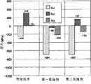
使用图19和20中所示的模拟结果描述第三和第四实施例的效果。对于n型晶体管,结果与第二实施例中相同,因此其描述省略。图19示出根据传统技术、第一实施例、第三实施例和第四实施例的p型晶体管中的应力模拟结果。此外,图20示出各种情况下的迁移率增强因子的比较。Effects of the third and fourth embodiments are described using the simulation results shown in FIGS. 19 and 20 . For the n-type transistor, the result is the same as in the second embodiment, so its description is omitted. FIG. 19 shows stress simulation results in p-type transistors according to the conventional technique, the first embodiment, the third embodiment, and the fourth embodiment. In addition, FIG. 20 shows a comparison of mobility enhancement factors in various cases.
如图19所示,形成在p型晶体管中的第二层中的第三应力施加膜23在第三实施例中是具有张应力的膜,根据此效应,Syy的压应力值变得比第一实施例的大。根据迁移率增强因子的公式,p型晶体管中的迁移率随着压应力Syy变大而变小。在第四实施例中,因为压应力源形成在源极/漏极区域中,所以沿沟道方向的压应力(Sxx)增大很多。As shown in FIG. 19, the third
如图20所示,在第三实施例中,因为沿深度方向的压应力(Syy)增大,与第一实施例相比,迁移率增强因子变小,但是与传统技术相比,迁移率提高。因为在第四实施例中沿沟道方向的压应力(Sxx)提高很大,所以可以获得较大的迁移率增强因子。在第三和第四实施例中,第二层中的应力施加膜由具有张应力的氮化硅膜形成,以不恶化n型晶体管中的迁移率增强;但是,当p晶体管中的迁移率增强重要时,第二层中的应力施加膜可以由具有压应力的压应力线性膜形成。As shown in Fig. 20, in the third embodiment, because the compressive stress (Syy) along the depth direction increases, the mobility enhancement factor becomes smaller compared with the first embodiment, but the mobility improve. Since the compressive stress (Sxx) in the channel direction is greatly improved in the fourth embodiment, a large mobility enhancement factor can be obtained. In the third and fourth embodiments, the stressor film in the second layer is formed of a silicon nitride film having tensile stress so as not to deteriorate the mobility enhancement in the n-type transistor; however, when the mobility in the p-transistor When reinforcement is important, the stress-applying film in the second layer may be formed of a compressively linear film having compressive stress.
参考图21的示意性剖面图描述根据本发明的半导体器件的另一个实施例(第五实施例)。Another embodiment (fifth embodiment) of the semiconductor device according to the present invention will be described with reference to the schematic sectional view of FIG. 21 .
如图21所示,根据第五实施例的半导体器件5的构造在于,基于已经参考图18所描述的第四实施例的半导体器件4中的p型晶体管中没有形成应力施加膜。即,作为应力施加膜,在n型晶体管中仅存在具有张应力的第一应力施加膜21和第三应力施加膜23。其它部件与半导体器件4中的相同。As shown in FIG. 21 , the
接着,描述根据本发明的制造半导体器件的方法的另一实施例(第五实施例)。这里,描述根据制造半导体器件5的方法。Next, another embodiment (fifth embodiment) of the method of manufacturing a semiconductor device according to the present invention is described. Here, a method according to manufacturing the
根据第五实施例的制造方法,在具有张应力的第一应力施加膜21上不形成具有压应力的第二应力施加膜,而是形成具有张应力的第三应力施加膜23,并且基于第四实施例的制造方法移除p型晶体管区域的第三应力施加膜23。其它工艺与第四实施例中的制造方法中相同。According to the manufacturing method of the fifth embodiment, the second
在第五实施例中,工艺比第四实施例中可以进一步缩短。此外,在n型晶体管中仅形成具有应力的应力施加膜(即具有张应力的第一应力施加膜21和第三应力施加膜23)。但是,在p型晶体管中,源极/漏极区域55和56通过外延生长由SiGe层形成,使得与第四实施例类似,源极/漏极区域55和56可以是应力施加源。据此,因为p型晶体管的沟道区域接受沿SiGe层沿沟道方向的压应力,所以在没有形成具有压应力的应力施加膜的情况下可以增强迁移率且提高晶体管性能。虽然第五实施例采用SiGe,但是不限于SiGe,只要其可以向沟道区域施加压应力。In the fifth embodiment, the process can be further shortened than in the fourth embodiment. In addition, only stress applying films having stress (ie, first
下面参考图22的示意性剖面结构图描述根据本发明的半导体器件的另一个实施例(第六实施例)。Another embodiment (sixth embodiment) of the semiconductor device according to the present invention will be described below with reference to the schematic sectional structural view of FIG. 22 .
如图22所示,第六实施例的半导体器件6构造在于,基于第五实施例的半导体器件5,具有张应力的第三应力施加膜23形成在整个表面上。其它部件与第五实施例中的半导体器件5中相同。As shown in FIG. 22 , the
接着,描述根据本发明的制造半导体器件的方法的另一实施例(第六实施例)。这里,描述半导体器件6的制造方法。Next, another embodiment (sixth embodiment) of the method of manufacturing a semiconductor device according to the present invention is described. Here, a method of manufacturing the
根据第六实施例的制造方法,基于第五实施例的制造方法,具有张应力的第三应力施加膜23形成在整个表面上,并且在p型晶体管区域中不移除第三应力施加膜23而保留。其它制造工艺与第五实施例中的制造方法中相同。According to the manufacturing method of the sixth embodiment, based on the manufacturing method of the fifth embodiment, the third
在第六实施例的半导体器件6,虽然具有张应力的第三应力施加膜以恶化p型晶体管的晶体管能力的方式工作,但是在栅电极形成之后形成第三应力施加膜,因此类似于第三实施例,其效果不大。此外,虽然具有张应力的第一应力施加膜和第三应力施加膜形成在n型晶体管的第一层和第二层中,但是为了缩短工艺的目的,第二层中的第三应力施加膜可以省略。In the
使用图23和24中所示的模拟结果描述第五和第六实施例的效果。n型晶体管与第二实施例中的情况下相同,因此其描述省略。图23示出根据传统技术、第一实施例、第五实施例和第六实施例的p型晶体管中的应力模拟结果。图24示出各种情况下的迁移率增强因子的比较。Effects of the fifth and sixth embodiments are described using the simulation results shown in FIGS. 23 and 24 . The n-type transistor is the same as in the case of the second embodiment, so its description is omitted. FIG. 23 shows stress simulation results in p-type transistors according to the conventional technique, the first embodiment, the fifth embodiment, and the sixth embodiment. Figure 24 shows a comparison of mobility enhancement factors for various cases.
如图23所示,根据第五实施例,因为包括SiGe的压应力源用在源极/漏极区域中,代替p型晶体管中的具有压应力的应力施加膜,它们与第一实施例取大致相同的值。因为在第六实施例中形成具有张应力的第三应力施加膜,压应力Sxx减小一定程度,并且压应力Syy增大许多。As shown in FIG. 23, according to the fifth embodiment, since a compressive stressor including SiGe is used in the source/drain region instead of the stressor film having compressive stress in the p-type transistor, they are the same as those of the first embodiment. roughly the same value. Since the third stress applying film having tensile stress is formed in the sixth embodiment, the compressive stress Sxx decreases to some extent, and the compressive stress Syy increases much.
如图24所示,在第五实施例中,因为沿横向方向的压应力(Sxx)增大,与第一实施例相比,迁移率增强因子变大。另一方面,在第六实施例中,因为压应力Syy由于具有张应力的第三应力施加膜23的效应而增大,迁移率增强因子基本与第一实施例的增强因子相同。与传统技术相比,两种情况都可以获得更高的迁移率增强因子。在第五和第六实施例中,p型晶体管中的源极/漏极区域55和56由SiGe形成,因此在沟道中施加压应力,而在n型晶体管中,n型晶体管中的源极/漏极区域35和36由具有张应力的层(诸如SiC等)形成,由此类似地得到源极/漏极区域35和36中具有应力施加源的结构。As shown in FIG. 24, in the fifth embodiment, since the compressive stress (Sxx) in the lateral direction increases, the mobility enhancement factor becomes larger compared with the first embodiment. On the other hand, in the sixth embodiment, since the compressive stress Syy increases due to the effect of the third
参考图25的示例性剖视结构图描述根据本发明的半导体器件的另一实施例(第七实施例)。Another embodiment (seventh embodiment) of the semiconductor device according to the present invention will be described with reference to an exemplary cross-sectional structural view of FIG. 25 .
如图25所示,根据第七实施例的半导体器件7构造在于,基于已经根据图11所述的第二实施例的半导体器件2,p型晶体管中的源极/漏极区域55和56由应力施加源形成。应力施加源例如由硅锗(SiGe)层形成。其他部件与半导体器件2中相同。As shown in FIG. 25, the
接着,描述根据本发明的制造半导体器件的方法的另一实施例(第七实施例)。这里,描述半导体器件7的制造方法。Next, another embodiment (seventh embodiment) of the method of manufacturing a semiconductor device according to the present invention is described. Here, a method of manufacturing the
根据第七实施例的制造方法,基于第二实施例的制造方法,p型晶体管中的源极/漏极区域55和56由应力施加源形成。应力施加源例如通过锗注入形成。或者,源极/漏极区域通过蚀刻移除,以形成沟槽,在沟槽部分中选择性地外延生长硅锗(SiGe)层。在此情况下,其他区域被绝缘膜覆盖,以保护其免于外延生长。绝缘膜在外延生长后移除。在第四实施例中,外延生长硅锗(SiGe)层用作具有压应力的应力施加源。锗(Ge)浓度例如为18%,但是锗浓度不限于此。虽然本实施例中采用SiGe,但是不限于SiGe,只要其能够向沟道区域施加压应力。According to the manufacturing method of the seventh embodiment, the source/
在第七实施例的半导体器件7中,与第三和第四实施例类似,通过外延生长而制造的SiGe层形成在p型晶体管的源极/漏极区域55和56中,并且与第二实施例类似,形成具有压应力的第二应力施加膜和第四应力施加膜。因此,来自SiGe层的压应力和来自第二和第三应力施加膜的压应力施加在p型晶体管下方的沟道区域,由此将较大的应力施加到沟道区域。此外,在n型晶体管中采用与第二实施例相同的结构,由此急剧增强n型晶体管和p型晶体管两者中的迁移率。In the
此外,在第七实施例中,诸如SiC等具有张应力的层形成在n型晶体管的源极/漏极区域中,由此得到源极/漏极区域中具有应力施加源的结构。Furthermore, in the seventh embodiment, a layer having tensile stress such as SiC is formed in the source/drain region of the n-type transistor, thereby obtaining a structure having a stress applying source in the source/drain region.
Claims (16)
Translated fromChineseApplications Claiming Priority (5)
| Application Number | Priority Date | Filing Date | Title |
|---|---|---|---|
| JP2007072968 | 2007-03-20 | ||
| JP072968/2007 | 2007-03-20 | ||
| JP2008018513AJP5003515B2 (en) | 2007-03-20 | 2008-01-30 | Semiconductor device |
| JP018513/2008 | 2008-01-30 | ||
| PCT/JP2008/053424WO2008126490A1 (en) | 2007-03-20 | 2008-02-27 | Semiconductor device and method for manufacturing the same |
Related Child Applications (1)
| Application Number | Title | Priority Date | Filing Date |
|---|---|---|---|
| CN2011100418396ADivisionCN102136429B (en) | 2007-03-20 | 2008-02-27 | Semiconductor device and method for manufacturing same |
Publications (2)
| Publication Number | Publication Date |
|---|---|
| CN101641780A CN101641780A (en) | 2010-02-03 |
| CN101641780Btrue CN101641780B (en) | 2011-12-21 |
Family
ID=39863646
Family Applications (2)
| Application Number | Title | Priority Date | Filing Date |
|---|---|---|---|
| CN2011100418396AActiveCN102136429B (en) | 2007-03-20 | 2008-02-27 | Semiconductor device and method for manufacturing same |
| CN2008800091111AActiveCN101641780B (en) | 2007-03-20 | 2008-02-27 | Semiconductor device and method for manufacturing the same |
Family Applications Before (1)
| Application Number | Title | Priority Date | Filing Date |
|---|---|---|---|
| CN2011100418396AActiveCN102136429B (en) | 2007-03-20 | 2008-02-27 | Semiconductor device and method for manufacturing same |
Country Status (6)
| Country | Link |
|---|---|
| US (8) | US9070783B2 (en) |
| JP (1) | JP5003515B2 (en) |
| KR (1) | KR101396422B1 (en) |
| CN (2) | CN102136429B (en) |
| TW (2) | TWI416635B (en) |
| WO (1) | WO2008126490A1 (en) |
Families Citing this family (23)
| Publication number | Priority date | Publication date | Assignee | Title |
|---|---|---|---|---|
| JP5003515B2 (en)* | 2007-03-20 | 2012-08-15 | ソニー株式会社 | Semiconductor device |
| US8030197B2 (en)* | 2009-05-04 | 2011-10-04 | Intel Corporation | Recessed channel array transistor (RCAT) in replacement metal gate (RMG) logic flow |
| JP5668277B2 (en)* | 2009-06-12 | 2015-02-12 | ソニー株式会社 | Semiconductor device |
| JP5456150B2 (en)* | 2010-02-17 | 2014-03-26 | パナソニック株式会社 | Semiconductor device and manufacturing method thereof |
| CN102214576A (en)* | 2010-04-09 | 2011-10-12 | 中国科学院微电子研究所 | Semiconductor device and method for manufacturing the same |
| JP5569173B2 (en)* | 2010-06-18 | 2014-08-13 | ソニー株式会社 | Semiconductor device manufacturing method and semiconductor device |
| JP5531812B2 (en) | 2010-06-23 | 2014-06-25 | 富士通セミコンダクター株式会社 | MOS transistor, method for manufacturing the same, and semiconductor integrated circuit device |
| JP5569243B2 (en) | 2010-08-09 | 2014-08-13 | ソニー株式会社 | Semiconductor device and manufacturing method thereof |
| CN102376575A (en)* | 2010-08-16 | 2012-03-14 | 中国科学院微电子研究所 | Method for forming source-drain stress region of MOS transistor and method for manufacturing MOS transistor |
| CN102386095B (en)* | 2010-08-31 | 2014-05-07 | 中国科学院微电子研究所 | Method for manufacturing semiconductor structure |
| CN102446726B (en)* | 2010-10-13 | 2013-10-09 | 中芯国际集成电路制造(上海)有限公司 | Method for forming metal gate |
| CN102487015A (en)* | 2010-12-03 | 2012-06-06 | 中国科学院微电子研究所 | A kind of semiconductor structure and its manufacturing method |
| CN102646588B (en)* | 2011-02-17 | 2015-06-24 | 中芯国际集成电路制造(上海)有限公司 | Manufacturing method of semiconductor device |
| US8421132B2 (en)* | 2011-05-09 | 2013-04-16 | International Business Machines Corporation | Post-planarization UV curing of stress inducing layers in replacement gate transistor fabrication |
| US8765561B2 (en)* | 2011-06-06 | 2014-07-01 | United Microelectronics Corp. | Method for fabricating semiconductor device |
| CN103681498B (en)* | 2012-09-12 | 2016-03-30 | 中芯国际集成电路制造(上海)有限公司 | A kind of manufacture method of semiconductor device |
| CN103107240B (en)* | 2012-12-06 | 2016-08-03 | 杭州赛昂电力有限公司 | Multi-crystal silicon film solar battery and preparation method thereof |
| JP2015032661A (en)* | 2013-08-01 | 2015-02-16 | ルネサスエレクトロニクス株式会社 | Semiconductor device, method for manufacturing the same, and method for mounting the semiconductor device |
| KR102302073B1 (en) | 2015-07-28 | 2021-09-14 | 삼성전자주식회사 | A semiconductor device and methods of manufacturing the same |
| US10026818B1 (en)* | 2017-01-19 | 2018-07-17 | Globalfoundries Inc. | Field effect transistor structure with recessed interlayer dielectric and method |
| US10276442B1 (en)* | 2018-05-30 | 2019-04-30 | Globalfoundries Inc. | Wrap-around contacts formed with multiple silicide layers |
| JP2021009971A (en)* | 2019-07-03 | 2021-01-28 | ソニーセミコンダクタソリューションズ株式会社 | Semiconductor device and manufacturing method |
| US12113131B2 (en)* | 2019-08-09 | 2024-10-08 | Hitachi Energy Ltd | Strain enhanced SiC power semiconductor device and method of manufacturing |
Citations (4)
| Publication number | Priority date | Publication date | Assignee | Title |
|---|---|---|---|---|
| CN1505839A (en)* | 2000-12-08 | 2004-06-16 | ������������ʽ���� | Semiconductor device |
| JP2005259945A (en)* | 2004-03-11 | 2005-09-22 | Sanyo Electric Co Ltd | Semiconductor device and manufacturing method thereof |
| US20070023795A1 (en)* | 2005-07-15 | 2007-02-01 | Kabushiki Kaisha Toshiba | Semiconductor device and method of fabricating the same |
| CN1925159A (en)* | 2005-08-30 | 2007-03-07 | 株式会社东芝 | Semiconductor device and method of fabricating same |
Family Cites Families (58)
| Publication number | Priority date | Publication date | Assignee | Title |
|---|---|---|---|---|
| JP2005057301A (en) | 2000-12-08 | 2005-03-03 | Renesas Technology Corp | Semiconductor device and method of manufacturing same |
| JP2002198368A (en)* | 2000-12-26 | 2002-07-12 | Nec Corp | Method for manufacturing semiconductor device |
| JP3974507B2 (en)* | 2001-12-27 | 2007-09-12 | 株式会社東芝 | Manufacturing method of semiconductor device |
| JP4173672B2 (en)* | 2002-03-19 | 2008-10-29 | 株式会社ルネサステクノロジ | Semiconductor device and manufacturing method thereof |
| US6573172B1 (en)* | 2002-09-16 | 2003-06-03 | Advanced Micro Devices, Inc. | Methods for improving carrier mobility of PMOS and NMOS devices |
| JP4557508B2 (en) | 2003-06-16 | 2010-10-06 | パナソニック株式会社 | Semiconductor device |
| US6939814B2 (en)* | 2003-10-30 | 2005-09-06 | International Business Machines Corporation | Increasing carrier mobility in NFET and PFET transistors on a common wafer |
| US7078282B2 (en)* | 2003-12-30 | 2006-07-18 | Intel Corporation | Replacement gate flow facilitating high yield and incorporation of etch stop layers and/or stressed films |
| US7154118B2 (en)* | 2004-03-31 | 2006-12-26 | Intel Corporation | Bulk non-planar transistor having strained enhanced mobility and methods of fabrication |
| JP2006093242A (en) | 2004-09-21 | 2006-04-06 | Sanyo Electric Co Ltd | Method of manufacturing semiconductor device |
| US7135724B2 (en)* | 2004-09-29 | 2006-11-14 | International Business Machines Corporation | Structure and method for making strained channel field effect transistor using sacrificial spacer |
| US7268049B2 (en)* | 2004-09-30 | 2007-09-11 | International Business Machines Corporation | Structure and method for manufacturing MOSFET with super-steep retrograded island |
| KR20070069160A (en) | 2004-10-29 | 2007-07-02 | 어드밴스드 마이크로 디바이시즈, 인코포레이티드 | Semiconductor device comprising semiconductor regions having different strained channel regions and method of manufacturing same |
| DE102004052617B4 (en)* | 2004-10-29 | 2010-08-05 | Advanced Micro Devices, Inc., Sunnyvale | A method of manufacturing a semiconductor device and semiconductor device having semiconductor regions having differently deformed channel regions |
| US7479684B2 (en)* | 2004-11-02 | 2009-01-20 | International Business Machines Corporation | Field effect transistor including damascene gate with an internal spacer structure |
| US7190036B2 (en)* | 2004-12-03 | 2007-03-13 | Taiwan Semiconductor Manufacturing Company, Ltd. | Transistor mobility improvement by adjusting stress in shallow trench isolation |
| JP2006165335A (en)* | 2004-12-08 | 2006-06-22 | Toshiba Corp | Semiconductor device |
| JP2006165355A (en) | 2004-12-09 | 2006-06-22 | Matsushita Electric Ind Co Ltd | Multilayer wiring board and manufacturing method thereof |
| JP4369379B2 (en)* | 2005-02-18 | 2009-11-18 | 富士通マイクロエレクトロニクス株式会社 | Semiconductor device |
| JP2006253317A (en)* | 2005-03-09 | 2006-09-21 | Fujitsu Ltd | Semiconductor integrated circuit device and p-channel MOS transistor |
| JP4426988B2 (en)* | 2005-03-09 | 2010-03-03 | 富士通マイクロエレクトロニクス株式会社 | Method for manufacturing p-channel MOS transistor |
| WO2006094835A1 (en) | 2005-03-11 | 2006-09-14 | Ryco Book Protection Services Limited | Method and apparatus for indirectly coating a substrate with a hot flowable viscous adhesive |
| JP4982958B2 (en)* | 2005-03-24 | 2012-07-25 | 富士通セミコンダクター株式会社 | Semiconductor device and manufacturing method thereof |
| JP4630728B2 (en)* | 2005-05-26 | 2011-02-09 | 株式会社東芝 | Semiconductor device and manufacturing method thereof |
| JP4605463B2 (en) | 2005-07-12 | 2011-01-05 | スズキ株式会社 | Canister piping structure |
| JP2007103654A (en) | 2005-10-04 | 2007-04-19 | Toshiba Corp | Semiconductor device and manufacturing method thereof |
| JP5114881B2 (en)* | 2005-07-26 | 2013-01-09 | 富士通セミコンダクター株式会社 | Semiconductor device and manufacturing method thereof |
| JP4997752B2 (en)* | 2005-12-13 | 2012-08-08 | ソニー株式会社 | Manufacturing method of semiconductor device |
| CN101366104B (en)* | 2006-02-08 | 2010-11-10 | 富士通半导体股份有限公司 | P channel MOS transistor and semiconductor integrated circuit equipment |
| US20070222035A1 (en)* | 2006-03-23 | 2007-09-27 | Taiwan Semiconductor Manufacturing Company, Ltd. | Stress intermedium engineering |
| US20070281405A1 (en)* | 2006-06-02 | 2007-12-06 | International Business Machines Corporation | Methods of stressing transistor channel with replaced gate and related structures |
| US7618866B2 (en)* | 2006-06-09 | 2009-11-17 | International Business Machines Corporation | Structure and method to form multilayer embedded stressors |
| JP5076388B2 (en)* | 2006-07-28 | 2012-11-21 | 富士通セミコンダクター株式会社 | Semiconductor device and manufacturing method thereof |
| WO2008038346A1 (en) | 2006-09-27 | 2008-04-03 | Fujitsu Limited | Semiconductor device and its manufacturing method |
| JP4501965B2 (en)* | 2006-10-16 | 2010-07-14 | ソニー株式会社 | Manufacturing method of semiconductor device |
| JP5380827B2 (en)* | 2006-12-11 | 2014-01-08 | ソニー株式会社 | Manufacturing method of semiconductor device |
| US20080157200A1 (en)* | 2006-12-27 | 2008-07-03 | International Business Machines Corporation | Stress liner surrounded facetless embedded stressor mosfet |
| DE102007004824A1 (en)* | 2007-01-31 | 2008-08-07 | Advanced Micro Devices, Inc., Sunnyvale | Improved stress transfer in an interlayer dielectric by using an additional stress layer over a dual strain layer in a semiconductor device |
| US20080191285A1 (en)* | 2007-02-09 | 2008-08-14 | Chih-Hsin Ko | CMOS devices with schottky source and drain regions |
| US20080217686A1 (en)* | 2007-03-09 | 2008-09-11 | International Business Machines Corporation | Ultra-thin soi cmos with raised epitaxial source and drain and embedded sige pfet extension |
| JP5003515B2 (en)* | 2007-03-20 | 2012-08-15 | ソニー株式会社 | Semiconductor device |
| US7534678B2 (en)* | 2007-03-27 | 2009-05-19 | Samsung Electronics Co., Ltd. | Methods of forming CMOS integrated circuit devices having stressed NMOS and PMOS channel regions therein and circuits formed thereby |
| US7989901B2 (en)* | 2007-04-27 | 2011-08-02 | Taiwan Semiconductor Manufacturing Company, Ltd. | MOS devices with improved source/drain regions with SiGe |
| US7867893B2 (en)* | 2007-06-28 | 2011-01-11 | International Business Machines Corporation | Method of forming an SOI substrate contact |
| JP2009016706A (en)* | 2007-07-09 | 2009-01-22 | Sony Corp | Semiconductor device and manufacturing method thereof |
| US20090050972A1 (en)* | 2007-08-20 | 2009-02-26 | Richard Lindsay | Strained Semiconductor Device and Method of Making Same |
| US7923321B2 (en)* | 2008-11-03 | 2011-04-12 | Taiwan Semiconductor Manufacturing Company, Ltd. | Method for gap filling in a gate last process |
| DE102008059648B4 (en)* | 2008-11-28 | 2011-12-22 | Advanced Micro Devices, Inc. | Greater ε gate electrode structure formed after transistor fabrication using a spacer |
| JP5434360B2 (en)* | 2009-08-20 | 2014-03-05 | ソニー株式会社 | Semiconductor device and manufacturing method thereof |
| US9087741B2 (en)* | 2011-07-11 | 2015-07-21 | International Business Machines Corporation | CMOS with dual raised source and drain for NMOS and PMOS |
| US8865595B2 (en)* | 2012-01-05 | 2014-10-21 | Taiwan Semiconductor Manufacturing Company, Ltd. | Device and methods for forming partially self-aligned trenches |
| US8841181B2 (en)* | 2012-03-07 | 2014-09-23 | United Microelectronics Corp. | Method for fabricating semiconductor device and PMOS device fabricated by the method |
| US9064948B2 (en)* | 2012-10-22 | 2015-06-23 | Globalfoundries Inc. | Methods of forming a semiconductor device with low-k spacers and the resulting device |
| US9064891B2 (en)* | 2013-07-16 | 2015-06-23 | Globalfoundries Inc. | Gate encapsulation achieved by single-step deposition |
| US9190272B1 (en)* | 2014-07-15 | 2015-11-17 | Samsung Electronics Co., Ltd. | Semiconductor device and method of fabricating the same |
| US20160268256A1 (en)* | 2015-03-13 | 2016-09-15 | Qualcomm Incorporated | Complementary metal-oxide semiconductor (cmos) transistor and tunnel field-effect transistor (tfet) on a single substrate |
| US10163704B2 (en)* | 2015-12-29 | 2018-12-25 | Taiwan Semiconductor Manufacturing Co., Ltd. | Semiconductor device and a method for fabricating the same |
| US9917082B1 (en)* | 2017-01-17 | 2018-03-13 | International Business Machines Corporation | Approach to fabrication of an on-chip resistor with a field effect transistor |
- 2008
- 2008-01-30JPJP2008018513Apatent/JP5003515B2/enactiveActive
- 2008-02-27WOPCT/JP2008/053424patent/WO2008126490A1/enactiveApplication Filing
- 2008-02-27USUS12/530,797patent/US9070783B2/enactiveActive
- 2008-02-27CNCN2011100418396Apatent/CN102136429B/enactiveActive
- 2008-02-27KRKR1020097015816Apatent/KR101396422B1/ennot_activeExpired - Fee Related
- 2008-02-27CNCN2008800091111Apatent/CN101641780B/enactiveActive
- 2008-03-11TWTW101109489Apatent/TWI416635B/enactive
- 2008-03-11TWTW097108537Apatent/TWI392029B/enactive
- 2015
- 2015-03-26USUS14/669,803patent/US9449974B2/enactiveActive
- 2016
- 2016-05-13USUS15/154,365patent/US9881920B2/enactiveActive
- 2017
- 2017-12-22USUS15/852,041patent/US10269801B2/enactiveActive
- 2019
- 2019-01-07USUS16/241,395patent/US10559567B2/enactiveActive
- 2019-12-26USUS16/727,218patent/US11011518B2/enactiveActive
- 2021
- 2021-04-30USUS17/245,638patent/US11664376B2/enactiveActive
- 2023
- 2023-04-06USUS18/296,793patent/US12342615B2/enactiveActive
Patent Citations (4)
| Publication number | Priority date | Publication date | Assignee | Title |
|---|---|---|---|---|
| CN1505839A (en)* | 2000-12-08 | 2004-06-16 | ������������ʽ���� | Semiconductor device |
| JP2005259945A (en)* | 2004-03-11 | 2005-09-22 | Sanyo Electric Co Ltd | Semiconductor device and manufacturing method thereof |
| US20070023795A1 (en)* | 2005-07-15 | 2007-02-01 | Kabushiki Kaisha Toshiba | Semiconductor device and method of fabricating the same |
| CN1925159A (en)* | 2005-08-30 | 2007-03-07 | 株式会社东芝 | Semiconductor device and method of fabricating same |
Also Published As
| Publication number | Publication date |
|---|---|
| US20200144262A1 (en) | 2020-05-07 |
| US9449974B2 (en) | 2016-09-20 |
| TWI416635B (en) | 2013-11-21 |
| US10559567B2 (en) | 2020-02-11 |
| US11011518B2 (en) | 2021-05-18 |
| US20230246032A1 (en) | 2023-08-03 |
| US12342615B2 (en) | 2025-06-24 |
| US10269801B2 (en) | 2019-04-23 |
| CN101641780A (en) | 2010-02-03 |
| CN102136429B (en) | 2013-10-30 |
| JP2008263168A (en) | 2008-10-30 |
| US20210265347A1 (en) | 2021-08-26 |
| US11664376B2 (en) | 2023-05-30 |
| US9070783B2 (en) | 2015-06-30 |
| US20180138179A1 (en) | 2018-05-17 |
| WO2008126490A1 (en) | 2008-10-23 |
| US20190157271A1 (en) | 2019-05-23 |
| KR20100014343A (en) | 2010-02-10 |
| US20160254259A1 (en) | 2016-09-01 |
| US20150200193A1 (en) | 2015-07-16 |
| TWI392029B (en) | 2013-04-01 |
| US9881920B2 (en) | 2018-01-30 |
| JP5003515B2 (en) | 2012-08-15 |
| TW201230209A (en) | 2012-07-16 |
| KR101396422B1 (en) | 2014-05-20 |
| CN102136429A (en) | 2011-07-27 |
| US20100102394A1 (en) | 2010-04-29 |
| TW200847300A (en) | 2008-12-01 |
Similar Documents
| Publication | Publication Date | Title |
|---|---|---|
| CN101641780B (en) | Semiconductor device and method for manufacturing the same | |
| TWI438867B (en) | CMOS device with different types and thicknesses of gate insulating layer and forming method thereof | |
| JP5326274B2 (en) | Semiconductor device and manufacturing method of semiconductor device | |
| TWI411109B (en) | Semiconductor device and method of manufacturing the same | |
| CN101207086B (en) | Formation method of semiconductor structure | |
| CN101924134B (en) | Semiconductor device and manufacturing method thereof | |
| JP2009500823A (en) | Techniques for forming contact insulation layers and silicide regions with different properties | |
| JP4771024B2 (en) | Manufacturing method of semiconductor device | |
| JP5092340B2 (en) | Semiconductor device and manufacturing method thereof | |
| JP5387700B2 (en) | Manufacturing method of semiconductor device | |
| JP2007294811A (en) | Semiconductor integrated circuit, and manufacturing method therefor | |
| JP2015084440A (en) | Semiconductor device |
Legal Events
| Date | Code | Title | Description |
|---|---|---|---|
| C06 | Publication | ||
| PB01 | Publication | ||
| C10 | Entry into substantive examination | ||
| SE01 | Entry into force of request for substantive examination | ||
| C14 | Grant of patent or utility model | ||
| GR01 | Patent grant |