CN101634770B - In-plane switching mode liquid crystal display device - Google Patents
In-plane switching mode liquid crystal display deviceDownload PDFInfo
- Publication number
- CN101634770B CN101634770BCN200910139978.5ACN200910139978ACN101634770BCN 101634770 BCN101634770 BCN 101634770BCN 200910139978 ACN200910139978 ACN 200910139978ACN 101634770 BCN101634770 BCN 101634770B
- Authority
- CN
- China
- Prior art keywords
- liquid crystal
- crystal layer
- comb
- molecules
- electrode
- Prior art date
- Legal status (The legal status is an assumption and is not a legal conclusion. Google has not performed a legal analysis and makes no representation as to the accuracy of the status listed.)
- Active
Links
- 239000004973liquid crystal related substanceSubstances0.000titleclaimsabstractdescription167
- 239000000758substrateSubstances0.000claimsabstractdescription96
- 230000005684electric fieldEffects0.000claimsabstractdescription54
- 239000010408filmSubstances0.000description98
- 239000011229interlayerSubstances0.000description39
- 239000011159matrix materialSubstances0.000description30
- 239000011521glassSubstances0.000description20
- 238000002834transmittanceMethods0.000description15
- 230000001681protective effectEffects0.000description14
- 238000000034methodMethods0.000description13
- 239000010410layerSubstances0.000description10
- 230000000087stabilizing effectEffects0.000description10
- 239000004065semiconductorSubstances0.000description9
- 239000010409thin filmSubstances0.000description8
- 230000005540biological transmissionEffects0.000description7
- 239000004988Nematic liquid crystalSubstances0.000description6
- 238000002347injectionMethods0.000description6
- 239000007924injectionSubstances0.000description6
- 238000004519manufacturing processMethods0.000description6
- 238000003825pressingMethods0.000description6
- 244000126211Hericium coralloidesSpecies0.000description4
- 229910004205SiNXInorganic materials0.000description4
- 229920000620organic polymerPolymers0.000description4
- 230000008569processEffects0.000description4
- 238000007789sealingMethods0.000description4
- 125000006850spacer groupChemical group0.000description4
- 229910021417amorphous siliconInorganic materials0.000description3
- 239000004020conductorSubstances0.000description3
- 230000006872improvementEffects0.000description3
- 239000004925Acrylic resinSubstances0.000description2
- 229920000178Acrylic resinPolymers0.000description2
- 239000004642PolyimideSubstances0.000description2
- NIXOWILDQLNWCW-UHFFFAOYSA-Nacrylic acid groupChemical groupC(C=C)(=O)ONIXOWILDQLNWCW-UHFFFAOYSA-N0.000description2
- 239000003990capacitorSubstances0.000description2
- 230000008859changeEffects0.000description2
- 230000008878couplingEffects0.000description2
- 238000010168coupling processMethods0.000description2
- 238000005859coupling reactionMethods0.000description2
- 230000007423decreaseEffects0.000description2
- 238000006073displacement reactionMethods0.000description2
- 230000000694effectsEffects0.000description2
- 230000001976improved effectEffects0.000description2
- 230000003071parasitic effectEffects0.000description2
- 229920001721polyimidePolymers0.000description2
- 230000009467reductionEffects0.000description2
- 238000003860storageMethods0.000description2
- VYZAMTAEIAYCRO-UHFFFAOYSA-NChromiumChemical compound[Cr]VYZAMTAEIAYCRO-UHFFFAOYSA-N0.000description1
- 229910052581Si3N4Inorganic materials0.000description1
- 230000009471actionEffects0.000description1
- 230000009286beneficial effectEffects0.000description1
- 230000001413cellular effectEffects0.000description1
- 239000003086colorantSubstances0.000description1
- 238000004040coloringMethods0.000description1
- 230000002950deficientEffects0.000description1
- 238000009826distributionMethods0.000description1
- 238000005516engineering processMethods0.000description1
- 230000002349favourable effectEffects0.000description1
- 238000003384imaging methodMethods0.000description1
- AMGQUBHHOARCQH-UHFFFAOYSA-Nindium;oxotinChemical compound[In].[Sn]=OAMGQUBHHOARCQH-UHFFFAOYSA-N0.000description1
- 230000005693optoelectronicsEffects0.000description1
- HQVNEWCFYHHQES-UHFFFAOYSA-Nsilicon nitrideChemical compoundN12[Si]34N5[Si]62N3[Si]51N64HQVNEWCFYHHQES-UHFFFAOYSA-N0.000description1
Images


Classifications
- G—PHYSICS
- G02—OPTICS
- G02F—OPTICAL DEVICES OR ARRANGEMENTS FOR THE CONTROL OF LIGHT BY MODIFICATION OF THE OPTICAL PROPERTIES OF THE MEDIA OF THE ELEMENTS INVOLVED THEREIN; NON-LINEAR OPTICS; FREQUENCY-CHANGING OF LIGHT; OPTICAL LOGIC ELEMENTS; OPTICAL ANALOGUE/DIGITAL CONVERTERS
- G02F1/00—Devices or arrangements for the control of the intensity, colour, phase, polarisation or direction of light arriving from an independent light source, e.g. switching, gating or modulating; Non-linear optics
- G02F1/01—Devices or arrangements for the control of the intensity, colour, phase, polarisation or direction of light arriving from an independent light source, e.g. switching, gating or modulating; Non-linear optics for the control of the intensity, phase, polarisation or colour
- G02F1/13—Devices or arrangements for the control of the intensity, colour, phase, polarisation or direction of light arriving from an independent light source, e.g. switching, gating or modulating; Non-linear optics for the control of the intensity, phase, polarisation or colour based on liquid crystals, e.g. single liquid crystal display cells
- G02F1/133—Constructional arrangements; Operation of liquid crystal cells; Circuit arrangements
- G02F1/1333—Constructional arrangements; Manufacturing methods
- G02F1/1343—Electrodes
- G02F1/134309—Electrodes characterised by their geometrical arrangement
- G02F1/134363—Electrodes characterised by their geometrical arrangement for applying an electric field parallel to the substrate, i.e. in-plane switching [IPS]
Landscapes
- Physics & Mathematics (AREA)
- Nonlinear Science (AREA)
- Geometry (AREA)
- Mathematical Physics (AREA)
- Chemical & Material Sciences (AREA)
- Crystallography & Structural Chemistry (AREA)
- General Physics & Mathematics (AREA)
- Optics & Photonics (AREA)
- Liquid Crystal (AREA)
Abstract
Description
Translated fromChinese本申请基于并要求于2008年7月22日提交的日本专利申请No.2008-188243的优先权,其公开内容通过引用全文合并于此。This application is based on and claims priority from Japanese Patent Application No. 2008-188243 filed on July 22, 2008, the disclosure of which is hereby incorporated by reference in its entirety.
技术领域technical field
本发明设计液晶显示(LCD)装置,更具体地,涉及面内切换(IPS)模式LCD装置。The present invention relates to liquid crystal display (LCD) devices, and more particularly, to in-plane switching (IPS) mode LCD devices.
背景技术Background technique
通常,LCD装置具有薄、重量轻和低功耗的特点。In general, LCD devices are characterized by thinness, light weight, and low power consumption.
具体地,利用有源元件驱动按照矩阵阵列布置的各个像素的有源矩阵寻址LCD(AM-LCD)曾经被认为是具有高图像质量的平板显示装置。特别是,使用薄膜晶体管(TFT)作为有源元件的AM-LCD装置被广泛地用作TFT-LCD装置。In particular, an Active Matrix Addressed LCD (AM-LCD), which uses active elements to drive individual pixels arranged in a matrix array, has been considered as a flat panel display device with high image quality. In particular, AM-LCD devices using thin film transistors (TFTs) as active elements are widely used as TFT-LCD devices.
利用夹在两个基板之间的TN(扭转向列)类型的液晶的电光效应的大多数TFT-LCD装置通过向液晶施加近似垂直于基板表面的电场从而引起液晶(LC)分子的位移,来显示图像。这些LCD装置被称作“垂直电场类型”。Most TFT-LCD devices that utilize the electro-optic effect of TN (twisted nematic) type liquid crystals sandwiched between two substrates induce displacement of liquid crystal (LC) molecules by applying an electric field to the liquid crystals approximately perpendicular to the surface of the substrates. Display the image. These LCD devices are called "vertical electric field type".
另一方面,一些LCD装置通过施加近似平行于基板表面的电场从而引起LC分子在平行于基板表面的平面中的位移,来进行成像。这些LCD装置被称作“横向电场类型”或“面内切换(IPS)模式”。同样也对IPS模式LCD装置进行了各种改进。下面将举例说明一些改进。On the other hand, some LCD devices perform imaging by applying an electric field approximately parallel to the substrate surface, thereby causing displacement of LC molecules in a plane parallel to the substrate surface. These LCD devices are called "lateral electric field type" or "in-plane switching (IPS) mode". Various improvements have also been made to the IPS mode LCD device as well. Some improvements are illustrated below.
在1974年公布的美国专利No.3,807,831(专利文献1)中公开了一种结构,在IPS模式LCD装置中使用彼此匹配的梳齿状电极(参见权利要求1、图1-4和图11)。In U.S. Patent No. 3,807,831 (Patent Document 1) published in 1974, a structure is disclosed using comb-tooth electrodes matched to each other in an IPS mode LCD device (see claim 1, FIGS. 1-4 and FIG. 11) .
在1981年公布的日本待审专利公布No.56-091277(专利文献1)中公开了一种技术,在利用TN类型液晶的电光效应的IPS模式AM-LCD装置中使用类似于上述专利文献1中的彼此匹配的梳齿状电极(见权利要求2,图7和图9至13)。该技术降低了公共电极和漏极总线之间的寄生电容,或公共电极和栅极总线之间的寄生电容。In Japanese Unexamined Patent Publication No. 56-091277 (Patent Document 1) published in 1981, a technique is disclosed in which a liquid crystal similar to the above-mentioned Patent Document 1 is used in an IPS mode AM-LCD device utilizing the electro-optical effect of a TN type liquid crystal. Comb-shaped electrodes that match each other (see claim 2, Figure 7 and Figures 9 to 13). This technique reduces the parasitic capacitance between the common electrode and the drain bus line, or the parasitic capacitance between the common electrode and the gate bus line.
在1995年公布的日本待审专利申请No.7-036058(专利文献3)中公开了一种技术,在使用TFT的AM-LCD装置中无需梳齿状电极来实现IPS模式LCD装置(参见权利要求1和5,图1至23)。利用该技术,在不同的层上形成公共电极和图像信号电极或公共电极和LC驱动电极,并且同时将公共电极或LC驱动电极形成为环形、交叉形、T形、∏(希腊字母Pi)形、H形或梯形。A technique is disclosed in Japanese Unexamined Patent Application No. 7-036058 (Patent Document 3) published in 1995 to realize an IPS mode LCD device without comb-shaped electrodes in an AM-LCD device using TFTs (see entitlement Requirements 1 and 5, Figures 1 to 23). Using this technology, common electrodes and image signal electrodes or common electrodes and LC driving electrodes are formed on different layers, and at the same time the common electrodes or LC driving electrodes are formed in a ring shape, cross shape, T shape, ∏ (Greek letter Pi) shape , H-shaped or trapezoidal.
在2002年公布的日本待审专利公开No.2002-323706(专利文献4)中公开了一种结构,用于产生LC驱动横向电场的像素电极和公共电极(二者均是梳齿形)位于总线(即,数据线)之上(即,更接近LC层的位置),该总线向用于驱动各个像素的有源元件提供信号,在该结构中,绝缘层位于像素电极和公共电极之间(见权利要求1,第一示例实施例,图1至2)。据称,利用该结构由于可以通过形成公共电极来覆盖总线以屏蔽来自总线的电场,防止由垂直串扰引起的缺陷显示。此外,据称,通过采用透明导电材料形成公共电极来增加孔径比。In Japanese Unexamined Patent Publication No. 2002-323706 (Patent Document 4) published in 2002, a structure is disclosed in which a pixel electrode and a common electrode (both comb-shaped) for generating a lateral electric field for LC driving are located at Above (i.e. closer to the LC layer) the bus (i.e., the data line) that provides signals to the active elements used to drive the individual pixels, in this structure an insulating layer is placed between the pixel electrode and the common electrode (See claim 1, first example embodiment, Figures 1 to 2). It is said that with this structure, since it is possible to shield the electric field from the bus lines by forming the common electrode to cover the bus lines, defective display caused by vertical crosstalk can be prevented. In addition, it is said that the aperture ratio is increased by forming the common electrode using a transparent conductive material.
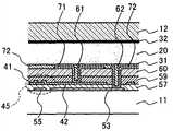
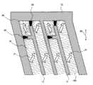
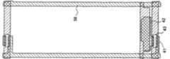
图11A至图11C是说明现有技术的普通IPS模式AM-LCD装置的结构示例的附图。图11A是装置的平面图,图11B是沿着图11A所示的I-I线的截面图,图11C是沿着图11A所示的II-II线的截面图。此外,图12A至图12D是示出了现有技术LCD装置的制造步骤的部分平面图。所有这些附图示出了一个像素区域的结构。11A to 11C are drawings illustrating a structural example of a related art general IPS mode AM-LCD device. 11A is a plan view of the device, FIG. 11B is a cross-sectional view along line I-I shown in FIG. 11A , and FIG. 11C is a cross-sectional view along line II-II shown in FIG. 11A . In addition, FIGS. 12A to 12D are partial plan views showing manufacturing steps of a related art LCD device. All these figures show the structure of one pixel region.
根据现有技术LCD装置,如图11A和图12B所示,通过沿着图11A和图12B的水平方向延伸的栅极总线55和沿着其垂直方向延伸的漏极总线56来形成矩形区域。在各个矩形区域中形成像素区域。像素整体上布置成矩阵阵列。According to the prior art LCD device, as shown in FIGS. 11A and 12B , a rectangular area is formed by
类似于栅极总线55,针对每一像素形成沿着图11A和图12B的水平方向延伸的公共总线53。在栅极总线55和漏极总线56的各个交叉点处,相对于各个像素形成TFT 45(见,图11A和图11B)。分别形成每一TFT45的漏电极41、源电极42和半导体薄膜43以具有图12B所示的图案或形状。Similar to the
产生液晶(LC)驱动电场的像素电极71和公共电极72分别配置彼此匹配或啮合的梳齿状部分(即,凸出至像素区域中的薄带形部分)。这里作为示例,像素电极71的梳齿状部分的数目为2,公共电极72的梳齿状部分的数目为1。The
如图11B所示,像素电极71通过相应的接触孔61电连接至TFT45的相应的源电极42,接触孔61穿过有机层间薄膜60和保护绝缘薄膜59。As shown in FIG. 11B , the
公共电极72通过相应的接触孔62电连接至相应的公共总线53,接触孔62穿过有机层间薄膜60、保护绝缘薄膜59和层间绝缘薄膜57。The
TFT 45的源电极42的一部分与相应的公共总线53重叠,从而通过重叠的部分形成像素区域的存储电容器。A part of the
在图11B和图11C中示出了现有技术LCD装置的截面结构,在图中,通过将有源矩阵基板和相对基板进行耦合和合并以将液晶层夹在其中来被配置该器件。A cross-sectional structure of a related art LCD device is shown in FIGS. 11B and 11C , in which the device is configured by coupling and combining an active matrix substrate and an opposing substrate to sandwich a liquid crystal layer therebetween.
有源矩阵基板包括:透明玻璃基板11、公共总线53、栅极总线55、漏极总线56、TFT 45、像素电极71和公共电极72,在玻璃基板11的内表面上形成上述所有结构。利用层间绝缘薄膜57覆盖直接形成在玻璃基板11的内表面上的公共总线53和栅极总线55。在层间薄膜57上形成TFT45的漏电极41、源电极42和半导体薄膜43以及漏极总线56。因此,公共总线53和栅极总线55通过层间绝缘薄膜57与漏电极41、电极42、半导体薄膜43和漏极总线56电绝缘。The active matrix substrate includes: a
除了形成接触孔61和62的区域以外,在玻璃基板11上形成的这些结构由保护绝缘薄膜59覆盖。通过在保护绝缘薄膜59上形成的有机层间薄膜60来找平由接触孔61和62引起的水平差。在有机层间薄膜60上形成像素电极71和公共电极72。These structures formed on the
如上所述,像素电极71通过相应的接触孔61电连接至相应的源电极42,并且公共电极72通过相应的接触孔62电连接至相应的公共总线53。此外,示意性示出了图11B和图11C的截面图,这些图不能如实地再现实际的水平差。As described above, the
利用由有机聚合物薄膜形成的取向薄膜31,覆盖其上形成了像素电极71和公共电极72的、具有上述结构的有源矩阵基板的表面。取向薄膜31的表面已经过取向处理,以使LC分子21的初始定位方向指向期望的方向(见图11A中的双向箭头30)。The surface of the active matrix substrate having the above-described structure on which the
另一方面,相对基板(即,彩色滤光器基板)包括:透明玻璃基板12;和形成使其与各个像素区域相对应的红(R)、绿(G)和蓝(B)的三原色层的彩色滤光器(未示出),以及在除了与各个像素区域相对应的那些区域以外的区域上形成遮光黑矩阵(未示出)。利用基于丙烯酸的外涂层薄膜(未示出)来覆盖在玻璃基板12的内表面上形成的彩色滤光器和黑矩阵。On the other hand, the opposite substrate (ie, the color filter substrate) includes: a
在外涂层薄膜的内表面上,形成柱状间隔区(未示出)来控制有源矩阵基板和相对基板之间的间隙。利用由有机聚合物膜形成的取向薄膜32来覆盖外涂层薄膜的内表面。取向薄膜32的表面已经过取向处理,以使LC分子21的初始定位方向指向期望的方向(见图11A的双向箭头30)。On the inner surface of the overcoat film, columnar spacers (not shown) are formed to control the gap between the active matrix substrate and the opposite substrate. The inner surface of the overcoat film is covered with an
分别具有上述结构的有源矩阵基板和相对基板以预定间隙彼此重叠,其方式使其表面朝内并且彼此相对,在其表面上分别形成取向薄膜31和32。将液晶20注入这两个基板之间的间隙。基板的周边由密封部件(未示出)密封,以封闭其中的液晶20。将一对偏振器板(未示出)分别布置在基板的外表面上。The active matrix substrate and the opposite substrate respectively having the above structures overlap each other with a predetermined gap in such a manner that their surfaces face inward and face each other, on which surfaces
如上所述,取向薄膜31和32的表面进行了一致的取向处理,其方式使得当没有施加电场时,沿着期望的方向平行地取向LC分子21。取向处理的取向方向是相对于像素和公共电极71和72的梳齿状部分延伸的方向(即,图11A中的垂直方向)顺时针地倾斜15度的方向。As described above, the surfaces of the
偏振器板对的透射轴(transmission axis)以直角相交。偏振器板对之一的透射轴与由一致取向处理确定的LC分子21的初始取向方向相同。The transmission axes of the pair of polarizer plates intersect at right angles. The transmission axis of one of the pair of polarizer plates is the same as the initial orientation direction of the
接着,以下将参照图12A至图12D来说明图11A至图11C所示的现有技术LCD装置的制造过程步骤。Next, manufacturing process steps of the prior art LCD device shown in FIGS. 11A to 11C will be described below with reference to FIGS. 12A to 12D .
以如下方式来制造有源矩阵基板。首先,在玻璃基板的表面之一上形成铬(Cr)薄膜并形成图案,从而形成具有如图12A所示的形状的公共总线53和栅极总线55。随后,在玻璃基板11的整个表面上形成由氮化硅(SiNx)薄膜形成的层间绝缘薄膜57来覆盖公共总线53和栅极总线55。The active matrix substrate was manufactured in the following manner. First, a chrome (Cr) thin film is formed and patterned on one of the surfaces of the glass substrate, thereby forming the
之后,形成半导体薄膜43(通常由非晶硅(a-Si)薄膜形成),以使层间绝缘薄膜57上的岛形图案与通过层间绝缘薄膜57相应的栅极总线55重叠。After that, a semiconductor film 43 (usually formed of an amorphous silicon (a-Si) film) is formed so that the island pattern on the
然后在层间绝缘薄膜57上形成另一Cr薄膜并形成图案,从而形成漏极总线56、漏电极41和源电极42(见图12B)。随后,由SiNx制成的保护绝缘薄膜59和由光敏丙烯酸树脂制成的有机层间薄膜61按该顺序连续层叠在层间绝缘薄膜57上,以覆盖该结构。Another Cr film is then formed and patterned on the
接着,形成穿过保护绝缘薄膜59和有机层间薄膜60的矩形接触孔61和穿过层间绝缘薄膜57、保护绝缘薄膜59和有机层间薄膜60的矩形接触孔62(见图12C)。Next, a
在有机层间薄膜60上形成透明导电材料的ITO(氧化铟锡)薄膜并形成图案,并从而在有机层间薄膜60上形成像素电极71和公共电极72。像素电极71通过相应的接触孔61与相应的源电极42接触。公共电极72通过相应的接触孔62与公共总线53接触(见图12D和图11B)。以这样的方式,制造有源矩阵基板的每一像素区域。An ITO (Indium Tin Oxide) thin film of a transparent conductive material is formed and patterned on the
以如下的方式制造相对基板(彩色滤光器基板)。首先,在玻璃基板12的表面之一上形成彩色滤光器(未示出)和遮光黑矩阵(未示出),随后,在玻璃基板12的整个表面上形成外涂层薄膜(未示出)来覆盖彩色滤光器和黑矩阵。然后,在外涂层薄膜上形成柱状间隔物(未示出)。以这样的方式,制造相对基板。The counter substrate (color filter substrate) was manufactured as follows. First, a color filter (not shown) and a light-shielding black matrix (not shown) are formed on one of the surfaces of the
分别在如上所述制造的有源矩阵基板的表面和相对基板的表面上形成由聚酰亚胺制成的取向薄膜31和32。
接着,对取向薄膜31和32的表面进行一致取向处理。然后将这两个基板重叠并具有固定间隙(例如,近似4.5μm),并且除了用于液晶的注入孔以外,通过密封部件对耦合后的基板的周边进行密封。Next, the surfaces of the
接着,在真空室内,通过注入孔将预定向列型液晶(例如,折射系数各向异性为0.067的向列型液晶)注入基板之间的间隙中,然后将注入孔密封。Next, in the vacuum chamber, a predetermined nematic liquid crystal (for example, a nematic liquid crystal having a refractive index anisotropy of 0.067) is injected into the gap between the substrates through the injection hole, and then the injection hole is sealed.
在以该方式将基板耦合并合并之后,分别将偏振器板(未示出)粘附在基板的外表面上。因此,完成具有图11A至图11C所示结构的现有技术IPS模式LCD装置。After the substrates are coupled and combined in this manner, polarizer plates (not shown) are adhered on the outer surfaces of the substrates, respectively. Thus, the prior art IPS mode LCD device having the structure shown in FIGS. 11A to 11C is completed.
对于上述现有技术IPS模式LCD装置,已知当施加LC驱动电场时,在一些区域(被称作“反向旋转域”)中LC分子被旋转至与一般旋转方向相反的方向。For the prior art IPS mode LCD device described above, it is known that when an LC driving electric field is applied, LC molecules are rotated to a direction opposite to the general rotation direction in some regions (referred to as "counter-rotation domains").
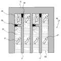
图13是示意性示出了图11-12所示的现有技术LCD装置中的反向旋转域的产生原理。为了便于说明,仅在图13中示出了像素电极71、公共电极72和LC分子21。在图13中,示意性示出了由像素电极71和公共电极72的梳齿状部分产生的LC驱动电场100(及其电力线)。FIG. 13 schematically shows the principle of generation of the reverse rotation field in the prior art LCD device shown in FIGS. 11-12. For convenience of illustration, only the
由LC分子21的初始取向方向30和LC驱动电场的方向之间的关系来限定LC分子21的旋转方向27(LC分子21的旋转在近似平行于有源矩阵基板和相对基板的平面产生)。The
因此,几乎在所有像素区域中LC分子21的旋转方向27是“顺时针”的。然而,如图13所示,在像素电极71的梳齿状部分的附近,LC驱动电场是放射状的。因此,在图中的阴影区域中LC分子21逆时针旋转。这意味着阴影区域是其中LC分子21逆时针旋转的反向旋转域80。Thus, the direction of
此外,在1998年公布的日本待审专利公布No.10-307295(专利文献5)公开了一种技术,用于产生横向电场的电极弯曲以有意地利用电极的弯曲部分使得在各个区域中LC分子的驱动(旋转)方向不同,从而降低了倾斜视角中的显示着色(见权利要求1、3和5,以及图1、2、4和6)。Furthermore, Japanese Unexamined Patent Publication No. 10-307295 (Patent Document 5) published in 1998 discloses a technique in which an electrode for generating a transverse electric field is bent to intentionally utilize the bent portion of the electrode so that in each region LC The molecules are driven (rotated) in different directions, thereby reducing display coloration in oblique viewing angles (see claims 1, 3 and 5, and Figures 1, 2, 4 and 6).
例如,提出了以下结构。具体地,使第一子区域中的LC分子的初始取向方向与第二子区域中的LC分组的初始取向方向相同。当施加电压时,第一和第二子区域中的LC分子彼此向相反的方向旋转,而同时保持LC分子的取向方向在第一和第二子区域中是对称的(见权利要求3)。采用该结构,优选地,通过平行电极对来产生驱动LC分子的横向电场,并将构成平行电极对的电极弯曲成V形(见权利要求5)。For example, the following structures are proposed. Specifically, the initial alignment direction of the LC molecules in the first subregion is the same as that of the LC groups in the second subregion. When a voltage is applied, the LC molecules in the first and second subregions rotate in opposite directions to each other while keeping the orientation directions of the LC molecules symmetrical in the first and second subregions (see claim 3). With this structure, preferably, a lateral electric field for driving LC molecules is generated by the pair of parallel electrodes, and the electrodes constituting the pair of parallel electrodes are bent into a V shape (see claim 5).
根据图13所示的传统配置,在梳齿状电极尖端部分的附近,LC驱动电场以放射形状分布,并且与液晶的初始取向方向相关联,形成(反向旋转域80),以使LC分子21与其旋转的预定方向相反地反向旋转。由于LC驱动电场在梳齿状电极尖端部分附近成平缓辐射形,在反向旋转域80和一般域70之间发生的暗域(即,边界域90)变得更大。除此以外,暗域的位置是不稳定的。According to the conventional configuration shown in FIG. 13, in the vicinity of the tip portion of the comb-shaped electrode, the LC driving electric field is distributed in a radial shape, and is associated with the initial alignment direction of the liquid crystal, forming (reverse rotation domain 80), so that the
因此,当将诸如手指按压等外部压力施加到显示表面时,反向旋转域80的状态(或,边界域90的位置)变得不稳定,并且在释放外部压力之后,留下手指按压痕迹。由于每一边界域90的宽度也变大,存在的问题是产生面板的光透射率的损耗。尽管反向旋转域80对光透射率有贡献,但是边界域90在白显示时(即,在施加电压时)仍旧是暗条件。Therefore, when an external pressure such as a finger press is applied to the display surface, the state of the reverse rotation domain 80 (or, the position of the boundary domain 90) becomes unstable, and after the external pressure is released, a finger press trace is left. Since the width of each
发明内容Contents of the invention
本发明的示例目的是提供一种ISP模式LCD装置,使得能够正确地固定反向旋转域的出现位置,并从而与传统上相比提供良好的画面质量和可靠性。An exemplary object of the present invention is to provide an ISP mode LCD device that enables correct fixing of an occurrence position of an inverse rotation domain and thereby provides good picture quality and reliability compared to conventional ones.
根据本发明示例方面的IPS模式液晶显示装置包括:An IPS mode liquid crystal display device according to an exemplary aspect of the present invention includes:
第一基板;first substrate;
第二基板,被布置成使其与第一基板相对;a second substrate arranged such that it is opposite to the first substrate;
液晶层,插入第一基板和第二基板之间;a liquid crystal layer interposed between the first substrate and the second substrate;
设置在第一基板上的第一电极部件,第一电极部件设置有梳齿状部分;a first electrode part disposed on the first substrate, the first electrode part being provided with a comb-shaped part;
设置在第一基板上的第二电极部件,以在第一电极部件与第二电极部件之间产生电场;以及a second electrode part disposed on the first substrate to generate an electric field between the first electrode part and the second electrode part; and
凸出电极部件,从梳齿状部分的靠近尖端部的部分和靠近底部的部分至少之一分支,使得在凸出电极部件与尖端部和底部之一的组合的整体平面形状中形成分支形状的L形部分。a protruding electrode member branching from at least one of a portion near the tip and a portion near the bottom of the comb-tooth-shaped portion so that a branched shape is formed in an overall planar shape of a combination of the protruding electrode member and one of the tip and the bottom L-shaped part.
附图说明Description of drawings
从以下结合附图的详细描述,本发明的示例特征和优点将变得显而易见,在附图中:Exemplary features and advantages of the present invention will become apparent from the following detailed description when taken in conjunction with the accompanying drawings, in which:
图1A是示出了根据本发明第一示例实施例的IPS模式AM-LCD装置的结构的平面图。FIG. 1A is a plan view showing the structure of an IPS mode AM-LCD device according to a first exemplary embodiment of the present invention.
图1B是沿着图1A所示的I-I线的截面图。FIG. 1B is a cross-sectional view along line I-I shown in FIG. 1A .
图1C是沿着图1A所示的II-II线的截面图。FIG. 1C is a cross-sectional view along line II-II shown in FIG. 1A .
图2A至图2D分别示出了根据第一示例实施例的IPS模式AM-LCD设备的制造方法的处理步骤的部分平面图。2A to 2D are partial plan views illustrating process steps of the method of manufacturing the IPS mode AM-LCD device according to the first exemplary embodiment, respectively.
图3是图1A所示的像素区域的上侧的放大部分平面图,指示在像素电极和公共电极之间施加电压并产生LC驱动电场时的状态。3 is an enlarged partial plan view of the upper side of the pixel region shown in FIG. 1A, indicating a state when a voltage is applied between a pixel electrode and a common electrode and an LC driving electric field is generated.
图4是图1A所示的像素区域的下侧的放大部分平面图,指示当在像素电极和公共电极之间施加电压并产生LC驱动电场时的状态。4 is an enlarged partial plan view of the lower side of the pixel region shown in FIG. 1A, indicating a state when a voltage is applied between a pixel electrode and a common electrode and an LC driving electric field is generated.
图5是示出了根据本发明第二示例实施例的IPS模式AM-LCD装置的结构的平面图。5 is a plan view showing the structure of an IPS mode AM-LCD device according to a second exemplary embodiment of the present invention.
图6是图5所示的像素区域的上侧的放大部分平面图,指示当在像素电极和公共电极之间施加电压并产生LC驱动电场时的状态。6 is an enlarged partial plan view of the upper side of the pixel region shown in FIG. 5, indicating a state when a voltage is applied between a pixel electrode and a common electrode and an LC driving electric field is generated.
图7是图5所示的像素区域的下侧的放大部分平面图,指示当在像素电极和公共电极之间施加电压并产生LC驱动电场时的状态。7 is an enlarged partial plan view of the lower side of the pixel region shown in FIG. 5, indicating a state when a voltage is applied between a pixel electrode and a common electrode and an LC driving electric field is generated.
图8是根据本发明第三示例实施例的IPS模式AM-LCD装置的像素区域的上侧的放大部分平面图,指示当在像素电极和公共电极之间施加电压并产生LC驱动电场时的状态。8 is an enlarged partial plan view of an upper side of a pixel region of an IPS mode AM-LCD device according to a third exemplary embodiment of the present invention, indicating a state when a voltage is applied between a pixel electrode and a common electrode and an LC driving electric field is generated.
图9是根据本发明第四示例实施例的IPS模式AM-LCD装置的像素区域的上侧的放大部分平面图,指示当在像素电极和公共电极之间施加电压并产生LC驱动电场时的状态。9 is an enlarged partial plan view of an upper side of a pixel region of an IPS mode AM-LCD device according to a fourth exemplary embodiment of the present invention, indicating a state when a voltage is applied between a pixel electrode and a common electrode and an LC driving electric field is generated.
图10是根据本发明第四示例实施例的IPS模式AM-LCD装置的像素区域的下侧的放大部分平面图,指示当在像素电极和公共电极之间施加电压并产生LC驱动电场时的状态。10 is an enlarged partial plan view of the lower side of a pixel region of an IPS mode AM-LCD device according to a fourth exemplary embodiment of the present invention, indicating a state when a voltage is applied between a pixel electrode and a common electrode and an LC driving electric field is generated.
图11A是示出了根据现有技术的IPS模式AM-LCD装置的结构的示例的平面图。FIG. 11A is a plan view showing an example of the structure of an IPS mode AM-LCD device according to the related art.
图11B是沿着图11A所示的I-I线的截面图。FIG. 11B is a cross-sectional view along line I-I shown in FIG. 11A .
图11C是沿着图11A所示的II-II线的截面图。FIG. 11C is a cross-sectional view along line II-II shown in FIG. 11A .
图12A至图12D是示出了图11所示的LCD装置的制造方法的处理步骤的部分平面图。12A to 12D are partial plan views showing process steps of the method of manufacturing the LCD device shown in FIG. 11 .
图13是图11所示的像素区域的上侧的放大部分平面图,指示当在像素电极和公共电极之间施加电压并产生LC驱动电场时的状态。13 is an enlarged partial plan view of the upper side of the pixel region shown in FIG. 11, indicating a state when a voltage is applied between a pixel electrode and a common electrode and an LC driving electric field is generated.
具体实施方式Detailed ways
将根据附图对本发明的示例实施例进行详细描述。Exemplary embodiments of the present invention will be described in detail with reference to the accompanying drawings.
本发明的IPS模式LCD装置的特征在于,梳齿状电极的尖端部具有分支形状,其中反向旋转域在其附近产生,使得在驱动液晶时每一分支形状围绕反向旋转域。在下文中,将参照附图对IPS模式LCD装置的具体结构进行描述。The IPS mode LCD device of the present invention is characterized in that the tip portion of the comb-teeth electrode has a branch shape in which a reverse rotation domain is generated in its vicinity so that each branch shape surrounds the reverse rotation domain when the liquid crystal is driven. Hereinafter, a specific structure of an IPS mode LCD device will be described with reference to the accompanying drawings.
[示例实施例1][Example Embodiment 1]
图1A至图1C示出了根据本发明第一示例实施例的IPS模式有源矩阵寻址LCD装置的结构。图1A是器件的部分平面图,图1B是沿着图1A所示的I-I线的部分截面图,以及图1C是沿着图1A所示的II-II线的部分截面图。图2A、图2B、图2C和图2D是分别示出了根据第一示例实施例的LCD装置的制造方法的处理步骤的部分平面图。所有这些附图均示出了一个像素区域的结构。1A to 1C illustrate the structure of an IPS mode active matrix addressing LCD device according to a first exemplary embodiment of the present invention. 1A is a partial plan view of the device, FIG. 1B is a partial cross-sectional view along line I-I shown in FIG. 1A , and FIG. 1C is a partial cross-sectional view along line II-II shown in FIG. 1A . 2A , 2B, 2C, and 2D are partial plan views respectively showing process steps of the method of manufacturing the LCD device according to the first exemplary embodiment. All of these drawings show the structure of one pixel region.
根据该LCD装置,如图1A和图2B所示,通过沿着图1A和图2B的水平方向延伸的栅极总线55和沿着图1A和图2B垂直反向延伸的漏极总线56而形成矩形区域。在各个矩形区域中形成像素区域。像素(和像素区域)整体布置成矩阵阵列。According to this LCD device, as shown in FIGS. 1A and 2B, a
类似于栅极总线55,针对每一像素形成公共总线53以沿着图1A和图2B的水平方向扩展。在栅极总线55的各个交叉点处,对应于各个像素形成漏极总线56、和TFT45(见图11A和图11b)。分别形成每一TFT45的漏电极41、源电极42和半导体薄膜43以具有图2B所示的图案或形状。Similar to the
产生LC驱动电场的像素电极71和公共电极72具有图1A所示的形状或图案。具体地,公共电极72包括:形成围绕像素区域的框架状的主要部分,以及从主要部分的上侧的中间向着主要部分的内空间中下侧延伸的梳齿状部分(即,在像素区域中向下凸出的薄带形部分)。The
公共电极72的主要部分与其它像素区域的公共电极(未示出)的主要部分一致。梳齿状部分的下(上)端不与其下侧接触。A main portion of the
另一方面,像素电极71位于公共电极72的矩形内空间中。像素电极71包括:形成与源电极42重叠的矩形板状主要部分,以及从主要部分的下侧的两端朝着主要部分的上侧延伸的两个梳齿状部分(即,在像素区域中向上凸出的两个薄带形部分)。On the other hand, the
在公共电极72的梳齿状部分的每一侧处布置这些梳齿状部分。因此,这些部分被布置为以这样的方式在像素区域中彼此匹配或啮合。These comb-tooth-shaped portions are arranged at each side of the comb-tooth-shaped portion of the
公共电极72的梳齿状部分和像素电极71的梳齿状部分在其每一侧之间的距离近似等于像素电极71的各个梳齿状部分和公共电极72的主要部分之间的距离。The distance between the comb-toothed portion of the
像素电极71的主要部分通过穿过有机层间薄膜60和保护绝缘薄膜59的相应的接触孔61连接至TFT45的相应的源电极42。The main part of the
公共电极72的主要部分通过穿过有机层间薄膜60、保护绝缘薄膜59和层间绝缘薄膜57的相应的接触孔62,电连接至相应的公共总线53。Main portions of the
它们的连接状态与图1B中所示的现有技术LCD装置的连接状态相同。TFT45的源电极42的部分通过层间绝缘薄膜57与相应的公共总线53重叠,从而通过重叠的部分形成像素区域的存储电容器。Their connection states are the same as those of the prior art LCD device shown in FIG. 1B. A portion of the
像素电极71的每一梳齿状部分在尖端部中具有分支形状。即,提供凸出部分以使其从每一梳齿状部分的靠近尖端部的部分分支,以及通过将梳齿状部分的凸出部分和尖端部组合到一起而形成的平面形状提供近似的L状形状。Each comb-tooth-shaped portion of the
仅在尖端部的所选侧上布置凸出部分,从而所选侧是这样的区域,其中,在该区域中,在没有这样分支形状(参照图13)情况下要在尖端部的附近产生的LC驱动电场引起与LC分子的一般旋转方向相反的LC分子的反向旋转。The protruding portion is arranged only on the selected side of the tip, so that the selected side is an area in which, in the absence of such a branch shape (refer to FIG. 13 ), would be produced in the vicinity of the tip The LC driving electric field induces a counter-rotation of the LC molecules that is opposite to the general direction of rotation of the LC molecules.
类似地,公共电极72的每一梳齿状部分在尖端部中具有分支形状。即,提供凸出部分以使其从公共电极72的每一梳齿状部分的靠近尖端部的部分分支,以及通过将梳齿状部分的凸出部分和尖端部组合到一起而形成的平面形状提供近似的L状形状。Similarly, each comb-tooth-shaped portion of the
仅在公共电极72的尖端部的所选侧上布置凸出部分,从而所选侧是这样的区域,其中,在该区域中,在没有这样分支形状(参照图13)情况下要在尖端部的附近产生的LC驱动电场引起与LC分子的一般旋转方向相反的LC分子的反向旋转。The protruding portion is arranged only on the selected side of the tip portion of the
此外,像素电极71的两个梳齿状部分之一还在其底端部(图1A的右侧)具有分支形状。即,提供凸出部分以使其从像素电极71的梳齿状部分的靠近右侧的底端部分的部分分支,以及通过将梳齿状部分的凸出部分和底端部组合到一起而形成的平面形状提供近似的L状形状。In addition, one of the two comb-tooth-shaped portions of the
仅在底端部的所选侧上布置凸出部分,从而所选侧是这样的区域,其中,在该区域中,在没有这样分支形状情况下要在底端部的附近产生的LC驱动电场引起与LC分子的一般旋转方向相反的LC分子的反向旋转。The protruding portion is arranged only on the selected side of the bottom end, so that the selected side is an area in which the LC drive electric field to be generated in the vicinity of the bottom end without such a branch shape A counter-rotation of the LC molecules is induced which is opposite to the general direction of rotation of the LC molecules.
对于像素电极71的两个梳齿状部分中的另一个(图1A中的左侧),由于在底端部的两侧没有产生LC分子的上述反向旋转,因此不存在具有分支形状的凸出部分。For the other of the two comb-tooth-shaped portions of the pixel electrode 71 (the left side in FIG. 1A ), since the above-mentioned reverse rotation of the LC molecules does not occur on both sides of the bottom end portion, there is no protrusion having a branched shape. out part.
对于公共电极72的梳齿状部分的底端部,尽管在其底端部的一侧处(图1A中的右侧)LC驱动电场引起LC分子的反向旋转,由于如上所述提供凸出部分以使其在公共电极72的梳齿状部分的底端部附近的那些区域处从像素电极71的梳齿状部分的靠近尖端部的部分分支,因此不存在具有分支形状的凸出部分。As for the bottom end portion of the comb-tooth-shaped portion of the
关于本发明的分支形状,可以对该分支进行构造以使得分成两个的分支部分被布置成相对于分支的起点而言是对称的关系,但是其形状无需如此。Regarding the branch shape of the present invention, the branch may be configured such that branch portions divided into two are arranged in a symmetrical relationship with respect to the starting point of the branch, but its shape need not be so.
此外,在该示例实施例中,尽管示出了公共电极72的一个梳齿状部分和像素电极71的两个梳齿状部分,但梳齿状部分的数目不限于图中所示的情况。Also, in this example embodiment, although one comb-tooth-shaped portion of the
在示出了根据本发明的示例实施例的结构的附图中,尽管指示每一电极的平面形状的轮廓是直的且角是直角,但是可以布置那些轮廓以使得按照斜方向延伸或具有曲线型式。可以使该轮廓的角的角度具有圆形。类似地,可以制成截面形状的电极,以具有包括相对基板表面斜侧边或曲线的此类形状。In the drawings showing the structure according to the exemplary embodiment of the present invention, although the outlines indicating the planar shape of each electrode are straight and the corners are right angles, those outlines may be arranged so as to extend in oblique directions or have curved lines. type. The angles of the corners of the profile can be rounded. Similarly, cross-sectionally shaped electrodes may be fabricated to have such shapes that include sloped sides or curves relative to the substrate surface.
在图1B和图1C中示出了根据第一示例实施例的LCD装置的截面结构,其中,通过将有源矩阵基板和相对基板进行耦合和合并以将液晶层夹在其间来配置该器件。A cross-sectional structure of an LCD device according to a first exemplary embodiment, in which the device is configured by coupling and merging an active matrix substrate and an opposing substrate to sandwich a liquid crystal layer therebetween, is shown in FIGS. 1B and 1C.
有源矩阵基板包括:透明玻璃基板11、公共总线53、栅极总线55、漏极总线56、TFT45、像素电极71和公共电极72,上述所有结构均在玻璃基板11的内表面上形成。利用层间绝缘薄膜57来覆盖直接在玻璃基板11的内表面上形成的公共总线53和栅极总线55。The active matrix substrate includes: a
在层间绝缘薄膜57上形成TFT45的漏电极41、源电极42和半导体薄膜43以及漏极总线56。因此,公共总线53和栅极总线55通过层间绝缘薄膜57与漏电极41、源电极42、半导体薄膜43和漏极总线56电绝缘。The
除了形成接触孔61和62的区域以外,利用保护绝缘薄膜59来覆盖在玻璃基板11上形成的这些结构。通过在保护绝缘薄膜59上形成的有机层间薄膜60对接触孔61和62引起的水平差进行找平。These structures formed on the
在有机层间薄膜60上形成像素电极71和公共电极72。如上所述,像素电极71通过相应的接触孔61与相应的源电极42电连接,并且公共电极72通过相应的接触孔62与相应的公共总线53电连接。A
示意性示出了图1B和图1C的截面图,从而不能如实地再现实际水平差。The cross-sectional views of FIGS. 1B and 1C are shown schematically, so that the actual level difference cannot be faithfully reproduced.
利用有机聚合物薄膜形成的取向薄膜31来覆盖在其上形成像素电极71和公共电极72的具有上述结构的有源矩阵基板的表面。已对取向薄膜31的表面进行取向处理,以使LC分子21的初始定向方向指向期望的方向(见图1A中的双向箭头30)。The
另一方面,相对基板包括:透明玻璃基板12;以及包括R、G和B三原色的彩色滤光器(未示出),和在除了与各个像素区域相对应的那些区域以外的区域中形成的遮光黑矩阵(未示出),上述二者均在玻璃基板12的内表面上形成。利用基于丙烯酸的外涂层薄膜(未示出)覆盖彩色滤光器和黑矩阵。On the other hand, the opposite substrate includes: a
在外涂层薄膜的内表面上,形成柱状间隔区(未示出)来控制有源矩阵基板和相对基板之间的间隙。利用由有机聚合物薄膜形成的取向薄膜32来覆盖外涂层薄膜的内表面。对取向薄膜32的表面进行取向处理,以使LC分子21的初始定位方向指向期望的方向(见图1A中的双向箭头30)。On the inner surface of the overcoat film, columnar spacers (not shown) are formed to control the gap between the active matrix substrate and the opposite substrate. The inner surface of the overcoat film is covered with an
分别具有上述结构的有源矩阵基板和相对基板以预定间隙彼此重叠,其方式为表面上的取向薄膜31和32向内并且彼此相对。将液晶20注入到两个基板之间的间隙中。基板的周边由密封部件(未示出)进行密封,以将液晶20限制在其中。将一对偏振器板分别布置在基板的外表面上。The active matrix substrate and the opposite substrate respectively having the above structures overlap each other with a predetermined gap in such a way that the
取向薄膜31和32的表面以如下的方式进行一致取向处理:如上所述,当没有施加电场时,LC分子21沿着期望的方向取向。取向处理的取向方向是相对于像素电极71和公共电极72的梳齿部分延伸的方向(即,图1A中的垂直方向)而言顺时针倾斜15度的方向。The surfaces of the
偏振器板对的光透射轴以直角相交。平行于由一致取向处理确定的LC分子的初始取向方向来布置偏振器板对之一的光透射轴。The light transmission axes of the polarizer plate pairs intersect at right angles. The light transmission axis of one of the pair of polarizer plates is arranged parallel to the initial orientation direction of the LC molecules determined by the uniform orientation process.
此外,LC分子21的初始取向方向(即,取向处理方向)是相对于像素和公共电极71和72的梳齿部分延伸的方向(即,图1A中的垂直方向)而言顺时针倾斜15度的方向。见图1A中的双向箭头30。为此,当将LC驱动电场100施加于LC分子21时,分子21将顺时针旋转(见图1A中的弯曲箭头27)。In addition, the initial alignment direction of the LC molecules 21 (i.e., the alignment treatment direction) is inclined 15 degrees clockwise with respect to the direction in which the comb-tooth portions of the pixels and
接着,以下将参照图2A至图2D来说明在图1A至图1C中所示的根据第一示例实施例的LCD装置的制造处理步骤。Next, manufacturing process steps of the LCD device according to the first exemplary embodiment shown in FIGS. 1A to 1C will be described below with reference to FIGS. 2A to 2D .
以如下方式来制造有源矩阵基板。首先,在玻璃基板11的表面上形成Cr薄膜并形成图案,从而形成分别具有图2A所示形状的公共总线53和栅极总线55。其后,在玻璃基板11的整个表面上形成由SiNx薄膜形成的层间绝缘薄膜57来覆盖公共总线53和栅极总线55。The active matrix substrate was manufactured in the following manner. First, a Cr thin film is formed and patterned on the surface of the
之后,在层间绝缘薄膜上形成半导体薄膜43(通常由a-Si薄膜形成),使其具有岛形图案,其方式使得半导体薄膜43通过层间绝缘薄膜57与相应的栅极总线55重叠。在层间绝缘薄膜57上形成另一Cr薄膜并形成图案,从而形成漏极总线56、漏电极41和源电极42(见图2B).Thereafter, a semiconductor film 43 (usually formed of an a-Si film) is formed on the interlayer insulating film to have an island pattern in such a manner that the
其后,由SiNx制成的保护绝缘薄膜59和由光敏丙烯酸树脂制成的有机层间薄膜60按照该顺序连续地层叠在层间绝缘薄膜57上。接着,形成穿过保护绝缘薄膜59和有机层间薄膜60的矩形接触孔61和穿过层间绝缘薄膜57、保护绝缘薄膜59和有机层间薄膜60的矩形接触孔62(见图2C)。Thereafter, a protective insulating
在有机层间薄膜60上形成透明导电材料的ITO薄膜并形成图案,从而在有机层间薄膜60上形成像素电极71和公共电极72。An ITO thin film of transparent conductive material is formed on the
像素电极71通过相应的接触孔61与相应的源电极42接触。公共电极72通过相应的接触孔62与公共总线53接触。以这样的方式,制造有源矩阵基板。The
以如下的方式来制造相对基板(例如,彩色滤光器基板)。首先,在玻璃基板12上形成彩色滤光器(未示出)和遮光黑矩阵(未示出),其后,在玻璃基板12的整个表面上形成外涂层薄膜(未示出)来覆盖彩色滤光器和黑矩阵。然后,在外涂层薄膜上形成柱状间隔区(未示出)。以这样的方式,制造相对基板。An opposite substrate (for example, a color filter substrate) is manufactured in the following manner. First, a color filter (not shown) and a light-shielding black matrix (not shown) are formed on the
在如上所制造的有源矩阵基板和相对基板上分别形成由聚酰亚胺制成的取向薄膜31和32。接着,对取向薄膜31和32的表面进行一致取向处理。然后使这两个基板重叠并具有固定间隙(例如,近似4.5μm),并且除了用于注入液晶的注入孔以外,通过密封部件对基板的周边进行密封。
接着,在真空室中,将预定向列液晶(例如,折射系数的各向异性为0.067的p类型向列液晶)通过注入孔注入到基板之间的间隙中,其后,将注入孔密封。Next, in a vacuum chamber, a predetermined nematic liquid crystal (eg, p-type nematic liquid crystal having a refractive index anisotropy of 0.067) was injected into the gap between the substrates through the injection hole, and thereafter, the injection hole was sealed.
在以这样的方式将基板耦合并合并后,分别将偏振器板(未示出)粘附在基板的外表面上。因此,完成了图1A至图1C所示的根据第一示例实施例的LCD装置。After the substrates are coupled and combined in this manner, polarizer plates (not shown) are respectively attached to the outer surfaces of the substrates. Thus, the LCD device according to the first exemplary embodiment shown in FIGS. 1A to 1C is completed.
可以使用n类型的向列液晶。在这种情况下,仅仅需要取向方向相对于上述角度改变90度,同时保持其它部件不变。在如下说明中,使用p类型向列液晶。An n-type nematic liquid crystal can be used. In this case, it is only necessary to change the orientation direction by 90 degrees with respect to the above-mentioned angle, while keeping other components unchanged. In the following description, a p-type nematic liquid crystal is used.
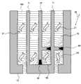
以下将参照图3和4对根据第一示例实施例的LCD装置的操作进行说明。在图3中,通过在像素电极71和公共电极72之间施加电压而产生的LC驱动电场100由表示电场电力线的虚线示出。此外,弯曲箭头27示出了由于LC驱动电场的动作而引起的LC分子21的旋转方向。在图4中,针对图1A中所示的像素区域的下侧示出了类似的状态。The operation of the LCD device according to the first exemplary embodiment will be described below with reference to FIGS. 3 and 4 . In FIG. 3 , the LC driving
如前所述,LC分子21的初始取向方向是相对于像素电极71和公共电极72的梳齿部分延伸的方向(即,图1A中的垂直方向)而言顺时针倾斜15度的方向。因此,当施加LC驱动电场时,在一般区域中分子21顺时针旋转。As previously described, the initial orientation direction of the
另一方面,如图3和图4所示,由于产生LC驱动电场,LC分子逆时针旋转并产生反向旋转域80,以使其相对于以下区域中附图的水平方向顺时针倾斜。On the other hand, as shown in FIGS. 3 and 4 , due to the generation of the LC driving electric field, the LC molecules rotate counterclockwise and generate a
第一区域(即,图3中所示的两个区域)是被在像素电极71的梳齿状部分的尖端部上提供的近似的L状形状和像素电极71的对面公共电极72(主要部分和梳齿状部分的底端部)包围的那些区域;The first region (i.e., the two regions shown in FIG. 3 ) is an approximate L-shape provided on the tip of the comb-tooth-shaped portion of the
第二区域(即,靠近图4的中心的区域)是被在公共电极72的梳齿状部分的尖端部上提供的近似的L状形状和公共电极72的对面像素电极71(即主要部分和梳齿状部分的底端部)包围的那些区域;以及The second area (i.e., the area near the center of FIG. 4 ) is an approximate L-shape provided on the tip of the comb-tooth-shaped portion of the
第三区域(即,靠近图4右侧的区域)是被在像素电极71的梳齿状部分的底端部上提供的近似的L状形状和像素电极71的对面公共电极72的主要部分包围的那些区域。The third region (i.e., the region near the right side of FIG. 4 ) is surrounded by an approximate L-shaped shape provided on the bottom end portion of the comb-tooth-shaped portion of the
在这些反向旋转域80和一般区域或一般域70之间形成边界域90,并因此甚至在向其施加电压时也产生暗条件。然而,由于在像素电极71和公共电极72上提供的分支形状的功能,那些边界域90被限制在小区域中。这是由于在作为边界的分支形状的凸出部分的两侧处极大地使LC驱动电场的倾斜方向反向,因此,在相应侧分别由强转矩引起顺时针旋转和逆时针旋转。
即,通过像素电极71和公共电极72上提供的分支形状的功能,可以在预定位置恰当地固定反向旋转域80和边界域90的产生位置。That is, by the function of the branch shape provided on the
因此,梳齿状电极尖端部附近中产生的反向旋转域80稳定,并因此由于外部压力(如手指按压)不能改变反向旋转域80的形状,手指按压痕迹很难留在显示屏幕上。Therefore, the
此外,因为可以紧密地控制在反向旋转域80和一般域70的边界部分发生的暗区域(即,边界域90),因此,可以提高作为显示要素的光透射率,并实现增加的亮度和功耗的降低。In addition, since the dark region (i.e., the boundary region 90) occurring at the boundary portion of the
以下,给出示例,并对与上述优点中提高光透射率相关的优点进行补充。当将该示例实施例应用于像素数为640像素(宽)×480像素(高)(×RGB)的10.4英寸类型LCD装置时,可以测量显示面板部分的光透射,并观察7.9%的透射率。Hereinafter, an example is given, and the advantages related to the improvement of the light transmittance among the above-mentioned advantages are supplemented. When this example embodiment is applied to a 10.4-inch type LCD device with a pixel number of 640 pixels (width)×480 pixels (height) (×RGB), the light transmission of the display panel portion can be measured, and a transmittance of 7.9% is observed .
另一方面,当使用现有技术配置的梳齿状电极但并不使用示例实施例的结构时,其光透射率为7.5%。该差值与通过本示例实施例的结构紧密控制边界域的改进效果相对应。On the other hand, when the comb-teeth electrodes configured in the prior art were used without using the structure of the example embodiment, the light transmittance thereof was 7.5%. This difference corresponds to the improved effect of tightly controlling the boundary domain by the structure of this example embodiment.
当通过日本待审专利申请No.1988-26767(专利文献6)(与包括本发明的相同发明人在内的发明人于1999年5月18日提交的美国专利No.5,905,556相对应)所示的锯片类型的电极形状完全抑制反向旋转域的发生时,所测量的面板的光透射率是7.2%。即,证实可以通过使用本示例实施例的结构来改进光投射率。As shown in Japanese Unexamined Patent Application No. 1988-26767 (Patent Document 6) (corresponding to U.S. Patent No. 5,905,556 filed on May 18, 1999 by inventors including the same inventor of the present invention) The light transmittance of the measured panel was 7.2% when the saw-blade-type electrode shape completely suppressed the occurrence of the reverse-rotation domain. That is, it was confirmed that the light projection rate can be improved by using the structure of the present exemplary embodiment.
[示例实施例2][Example Embodiment 2]
在图5中示出了根据本发明第二示例实施例的LCD装置。在该示例实施例的LCD装置的结构中,通过参照上述专利文献5中所公开的技术来将用于产生LC驱动电场的像素电极和公共电极布置成具有弯曲形状。An LCD device according to a second exemplary embodiment of the present invention is shown in FIG. 5 . In the structure of the LCD device of this example embodiment, the pixel electrode and the common electrode for generating an LC driving electric field are arranged to have a curved shape by referring to the technique disclosed in Patent Document 5 mentioned above.
该示例实施例不同于根据本发明第一示例实施例的结构之处在于如下要点:弯曲部分用于在LC驱动电场对其进行影响时有意地使LC分子的驱动方向针对每一区域而不同。This exemplary embodiment differs from the structure according to the first exemplary embodiment of the present invention in the point that the curved portion serves to intentionally make the driving direction of LC molecules different for each region when the LC driving electric field affects it.
除此以外其它要点是与第一示例实施例的相同结构。因此,利用第一示例实施例的情况中的相同参考数字来表示两个示例实施例中的相同部件,并从而省略对这些相同部件的描述。The other points are the same structure as that of the first exemplary embodiment. Therefore, the same reference numerals as in the case of the first exemplary embodiment are used to denote the same components in both example embodiments, and thus the description of these same components is omitted.
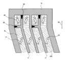
在该第二示例实施例中,如图5所示,尽管产生LC驱动电场的像素电极71和公共电极72使相互啮合的梳齿状部分类似于第一示例实施例的结构,但梳齿状部分弯曲,以具有近似的V形,其中直边界线500根据在接近像素区域的中心部分处沿着图5中的水平方向延伸。与上述相对应,同样使沿着图5的垂直方向延伸的漏极总线56弯曲,以及具有近似的V形。因此,同样使像素区域的形状弯曲以具有近似的V形。In this second exemplary embodiment, as shown in FIG. 5 , although the
在弯曲位置将像素区域分成边界线500的上侧上的第一子区域1和边界线500的下侧上的第二子区域2。以预定角度使像素电极71和公共电极72弯曲,使得它们相对于第一子区域1中附图的垂直方向逆时针弯曲,并且它们在第二子区域中以与第一子区域1相同的角度顺时针弯曲。The pixel area is divided into a first sub-area 1 on the upper side of the boundary line 500 and a second sub-area 2 on the lower side of the boundary line 500 at the curved position. The
设置LC分子21的定向处理方向,以使得在没有施加电压时沿着垂直方向(参照图5中双向箭头30)平行地确定LC分子21的方向。The orientation processing direction of the
对于每一区域中像素电极71和公共电极72的延伸方向的角度(或偏斜角)而言,期望其值在相对于定向处理方向的±10度至±25度量级范围内的值,例如,这可以使其角度为±15度量级(在第一子区域1中逆时针的15度和第二子区域2中的顺时针15度)。For the angle (or skew angle) of the extension direction of the
尽管LC驱动阈值电压降低,但如果使偏斜角较大,则用于实现最大透射率的峰值电压增加。即,相对于所施加的电压的光透射率曲线变得缓和。Although the LC driving threshold voltage decreases, if the off-angle angle is made larger, the peak voltage for achieving maximum transmittance increases. That is, the light transmittance curve with respect to the applied voltage becomes gentle.
相反地,当偏移电压小时,光透射率曲线变得陡峭。如果偏斜角变大,梳齿状电极的弯曲部分处的LC域的边界位置易于稳定固定。Conversely, when the offset voltage is small, the light transmittance curve becomes steep. If the off-angle angle becomes large, the boundary position of the LC domain at the bent portion of the comb-tooth-shaped electrode tends to be stably fixed.
当施加LC驱动电压时,沿着相对于附图中水平方向(直边界线500的方向)逆时针略微倾斜的方向,在第一子区域1中的主区域中产生LC驱动电场,而沿着相对于附图中水平方向顺时针略微倾斜方向,在第二子区域2中的主区域中产生LC驱动电场。When an LC driving voltage is applied, an LC driving electric field is generated in the main region in the first subregion 1 along a direction slightly inclined counterclockwise with respect to the horizontal direction (the direction of the straight boundary line 500) in the drawing, while along The LC driving electric field is generated in the main area in the second sub-area 2 in a slightly inclined direction clockwise relative to the horizontal direction in the drawing.
因此,通过LC驱动电场,在没有施加电压时沿着附图中垂直方向一致定向的LC分子21在第一子区域1中主要顺时针旋转,而在第二子区域2中LC分子21主要逆时针旋转。因此,通过在第一子区域1和第二子区域2中LC分子的旋转方向彼此不同,有利的是可以抑制由于视角的改变而引起的显示着色。Therefore, by the LC driving electric field, the
在第二示例实施例中,类似于第一示例实施例的结构向像素电极71和公共电极72提供分支形状。如图6和图7所示,通过分支形状的功能,可以在预定位置上恰当地固定在第一子区域1和第二子区域2中分别产生的反向旋转域80的位置和边界域90的位置。In the second exemplary embodiment, a branch shape is given to the
因此,在梳齿状电极尖端部的附近产生的反向旋转域80稳定,并因此由于外部压力(如手指按压)不能改变反向旋转域80的形状,手指按压痕迹很难留在显示屏幕上。Therefore, the
此外,由于可以紧密控制在反向旋转域80和一般域70的边界部分发生的暗区域或边界域90,因此,可能提高作为显示要素的光透射率,并实现增加的亮度和功耗的降低。In addition, since the dark region or
此外,在该第二示例实施例中,布置像素电极71和公共电极72的梳齿状部分的尖端部的分支形状,以使其中之一沿着平行于LC分子的初始取向方向的方向进行布置,而另一个沿着垂直于上述初始取向方向的方向进行布置。Furthermore, in this second exemplary embodiment, the branch shapes of the tip portions of the comb-tooth-shaped portions of the
此外,通过将该分支形状部分,和与其面对、用于产生LC驱动电场的电极进行组合,形成通过组合方括号对而布置的平面形状(即,作为由像素电极71的电极部分或公共电极72的电极部分之一组成的分支形部分的一个部分,和面对上述一个部分的其它电极的另一个部分的组合)。Furthermore, by combining this branch shape portion, and an electrode facing it for generating an LC driving electric field, a planar shape arranged by combining a pair of square brackets (that is, as an electrode portion formed by the
采用这样的形状,能够产生大致一致地向LC分子的初始取向方向倾斜的电场,并能够稳固地固定上述反向旋转域80。With such a shape, it is possible to generate an electric field inclined substantially uniformly in the direction of the initial orientation of the LC molecules, and to firmly fix the aforementioned
当假设“组合方括号对的形状”是矩形时,选择长边和短边的比值为2∶1至3∶1的量级,并且将其长边设置成使其与LC分子的初始取向方向平行,该区域中的LC分子的旋转角度将与梳齿电极(即像素电极71和公共电极72)彼此平行伸展的区域中LC分子的旋转角度几乎一致(即,相对所施加的电压的光透射率曲线几乎相同)。When it is assumed that the "shape of the pair of combined square brackets" is a rectangle, the ratio of the long side to the short side is selected to be on the order of 2:1 to 3:1, and its long side is set so that it is aligned with the initial orientation direction of the LC molecules Parallel, the rotation angle of the LC molecules in this region will be almost the same as the rotation angle of the LC molecules in the region where the comb electrodes (i.e. the
因此,所产生的电场有效地对光透射有贡献,并有利于显示装置。当长边和短边的比值小于2∶1-3∶1的关系时,该区域内的LC驱动电场的倾斜度变大,即,将出现与以下特征相对应的状态,梳齿电极的延伸方向和LC分子的初始取向方向之间的大角度(即,偏斜角)状态。Therefore, the generated electric field effectively contributes to light transmission and is beneficial to the display device. When the ratio of the long side to the short side is less than the relationship of 2:1-3:1, the inclination of the LC driving electric field in this region becomes larger, that is, a state corresponding to the following characteristics will appear, the extension of the comb-teeth electrode The state of large angles (ie, skew angles) between the orientation and the initial orientation direction of the LC molecules.
换言之,LC驱动阈值电压降低,用于实现最大透射率的峰值电压增加。相对所施加电压的透射率因子的曲线变得缓和。相反,当其比值大时,该区域中的LC驱动电场的倾斜度变小,即,将获得当偏斜角小时的相应特性。尽管如上所述大约2∶1-3∶1的上述比值是最令人期望的,但是使其处于大约1∶1至4∶1的范围内是可能的。In other words, the LC driving threshold voltage decreases and the peak voltage for achieving maximum transmittance increases. The curve of the transmittance factor versus applied voltage becomes gentler. On the contrary, when the ratio thereof is large, the inclination of the LC driving electric field in this region becomes small, that is, the corresponding characteristics when the off-angle angle is small will be obtained. It is possible to have the above ratio in the range of about 1:1 to 4:1, although as stated above about 2:1-3:1 is most desirable.
在该示例实施例中,如上所述,尽管梳齿状部分的两个尖端部的延伸方向是垂直的并分别平行于LC分子的初始取向方向,以使产生倾斜于期望方向、符合这种关系的LC驱动电场,但在尖端部的两个延伸方向和LC分子的初始取向方向之间不需要存在这样严格的关系,而是偏离上述期望关系一些也是可能的。In this exemplary embodiment, as described above, although the extension directions of the two tip portions of the comb-tooth-shaped portion are perpendicular and respectively parallel to the initial orientation directions of the LC molecules, so that the generation of an inclination to the desired direction conforms to this relationship The LC driving electric field, but there need not be such a strict relationship between the two extension directions of the tip and the initial orientation direction of the LC molecules, but some deviation from the above desired relationship is also possible.
然而,期望各自的关系被设置为小于梳齿状部分的主要部分的延伸方向和LC分子的初始取向方向之间的偏斜角(在上述示例中,15度)。However, it is desirable that the respective relationships are set to be smaller than the off angle (in the above example, 15 degrees) between the extension direction of the main portion of the comb-tooth-shaped portion and the initial alignment direction of the LC molecules.
[示例实施例3][Example Embodiment 3]
在图8中示出了本发明的第三示例实施例的特征。可以使梳齿电极尖端部的分支形状具有如图8中所示的形状。如图8所示,通过分支形状的功能,在第一子区域1和第二子区域2中的反向旋转域80和边界域90的产生位置分别可以恰当地固定在预定位置上。Features of a third exemplary embodiment of the present invention are shown in FIG. 8 . The branched shape of the tip portion of the comb-teeth electrode may be made to have a shape as shown in FIG. 8 . As shown in FIG. 8 , by the function of the branch shape, the generation positions of the
因此,在梳齿电极尖端部附近中产生的反向旋转域80稳定,并因此由于诸如手指按压的外部压力不能改变反向旋转域80的形状,手指按压痕迹很难保留在显示屏幕上。Therefore, the
除了上述内容,其它部分与第一示例实施例的结构相同。因此,两个示例实施例中的相同元件由在第一示例实施例的情况下的相同附图标记表示,并因此省略对它们的描述。Except for the above, other parts are the same as the structure of the first exemplary embodiment. Therefore, the same elements in the two exemplary embodiments are denoted by the same reference numerals in the case of the first exemplary embodiment, and thus their descriptions are omitted.
除了如图8所示的形状之外,各种形状是可能的,以使分支中的凸出部分可以被弯曲和成为曲线形。关于电极的形状,第二示例实施例所示的形状是更令人期望的。这是由于第二示例实施例在反向旋转域80中具有更高的光透射率。Various shapes are possible other than the one shown in FIG. 8 so that the protrusions in the branches can be bent and curvilinear. Regarding the shape of the electrodes, the shape shown in the second exemplary embodiment is more desirable. This is due to the higher light transmittance in the
[示例实施例4][Example Embodiment 4]
在图9和图10中示出了本发明的第四示例实施例的特征。在该示例实施例中,尽管梳齿电极自身的尖端部没有形成分支形状,但是其设置有用于使反向旋转域80稳定的T形稳定电极560,以使其与梳齿电极的尖端部重叠。通过结合稳定电极和梳齿状电极而形成的平面形状具有与第二示例实施例的梳齿电极的形状类似的特征。Features of a fourth exemplary embodiment of the present invention are shown in FIGS. 9 and 10 . In this example embodiment, although the tip portion of the comb-teeth electrode itself is not formed into a branch shape, it is provided with a T-shaped stabilizing
通过使用在相同层上形成漏极总线56(见图1C)的Cr薄膜来形成具有与像素电极71重叠部分的稳定电极560,同时通过使用在相同层上形成栅极总线55和公共总线53(见图1B)的另一Cr薄膜来形成具有与公共电极72重叠部分的稳定电极550。The stabilizing
由于在与梳齿状电极重叠部分处形成电容的作用,稳定电极具有与重叠的梳齿电极近似相同的电势,所以在这样的配置中也可以获得本发明的优点。The advantages of the present invention can also be obtained in such a configuration as the stabilizing electrode has approximately the same potential as the overlapping comb-shaped electrodes due to the effect of forming a capacitance at the overlapped portions of the comb-shaped electrodes.
如下列出本发明的应用示例。IPS-模式LCD装置和其它装置同样使用在如计算机监视器、LCD电视机、蜂窝电话、GPS(全球定位系统)终端、汽车导航系统、游戏机、银行和便利店的终端显示器和医疗诊断设备中。Application examples of the present invention are listed below. IPS-mode LCD devices and others are also used in devices such as computer monitors, LCD televisions, cellular phones, GPS (Global Positioning System) terminals, car navigation systems, game machines, terminal displays in banks and convenience stores, and medical diagnostic equipment .
根据本发明的另一示例方面的IPS模式液晶显示装置包括插入第一基板和第二基板之间的液晶层。第一基板设置有具有梳齿状部分的第一电极部件和第二电极部件从而第一电极部件和第二电极部件之间产生电场。此外,在梳齿状部分的靠近尖端部的部分和靠近底部的部分至少之一上提供用于稳定反向旋转域的稳定电极部件,以使其经由绝缘薄膜与梳齿状部分重叠。稳定电极部件的一部分设置有从梳齿状部分延伸的凸出部分,从而在稳定电极部件的凸出部分和尖端部和底部之一的组合的整体平面形状中形成分支形状的L形部分。An IPS mode liquid crystal display device according to another exemplary aspect of the present invention includes a liquid crystal layer interposed between a first substrate and a second substrate. The first substrate is provided with a first electrode part having a comb-teeth part and a second electrode part such that an electric field is generated between the first electrode part and the second electrode part. In addition, a stabilizing electrode member for stabilizing the reverse rotation domain is provided on at least one of the comb-tooth-shaped portion near the tip and the bottom so as to overlap the comb-tooth-shaped portion via the insulating film. A part of the stabilizing electrode member is provided with a protruding portion extending from the comb-shaped portion to form a branch-shaped L-shaped portion in an overall planar shape of a combination of the protruding portion and one of the tip and the bottom of the stabilizing electrode member.
由于上述电极形状的特征,可以确定在梳齿电极的尖端部和与其相对的电极之间产生的电场分布,并且可以稳定地固定一般域和在该区域产生的反向旋转域之间的边界。Due to the characteristics of the electrode shape described above, the electric field distribution generated between the tip portion of the comb-teeth electrode and the electrode opposed thereto can be determined, and the boundary between the general domain and the counter-rotation domain generated in this region can be stably fixed.
因此,在梳齿电极尖端部的附近产生的反向旋转域稳定,并从而由于诸如手指按压的外部压力不能改变反向旋转域的形状,手指按压痕迹很难保留在显示屏幕上。此外,由于可以紧密地控制在反向旋转域和一般域的边界部分发生的暗域(即,边界域),因此,可能提高作为显示元素的透射因子,并实现亮度增加或减少功耗。Therefore, the reverse rotation field generated in the vicinity of the tip portion of the comb-teeth electrode is stable, and thus since the shape of the reverse rotation field cannot be changed by external pressure such as a finger press, finger press traces hardly remain on the display screen. In addition, since the dark field (ie, boundary field) occurring at the boundary portion of the reverse rotation field and the general field can be tightly controlled, it is possible to increase the transmittance factor as a display element, and to achieve increased brightness or reduced power consumption.
根据本发明的IPS模式LCD装置,通过将具有分支形状的这种固定结构应用于反向旋转域,本发明使得能够恰当地固定反向旋转域的发生位置,并从而提供与传统器件相比良好的画面质量和可靠性。According to the IPS mode LCD device of the present invention, by applying such a fixing structure having a branched shape to the reverse rotation domain, the present invention enables to properly fix the occurrence position of the reverse rotation domain, and thus provides a favorable picture quality and reliability.
尽管参照本发明的示例实施例已具体示出并描述了本发明,但本发明不限于这些实施例。本领域普通技术人员将理解的是,在不背离权利要求所限定的本发明的精神和范围的前提下,可以在形式和细节上进行各种改变。Although the invention has been particularly shown and described with reference to exemplary embodiments of the invention, the invention is not limited to these embodiments. It will be understood by those of ordinary skill in the art that various changes in form and details may be made without departing from the spirit and scope of the present invention as defined in the claims.
此外,即使在审查中修改权利要求,发明人的目的也是保留所要求保护的本发明的所有等同物。Furthermore, it is the inventor's intent to retain all equivalents of the claimed invention even if the claims are amended during prosecution.
Claims (13)
Translated fromChineseApplications Claiming Priority (3)
| Application Number | Priority Date | Filing Date | Title |
|---|---|---|---|
| JP2008188243 | 2008-07-22 | ||
| JP2008188243AJP5266578B2 (en) | 2008-07-22 | 2008-07-22 | Horizontal electric field type liquid crystal display device |
| JP2008-188243 | 2008-07-22 |
Publications (2)
| Publication Number | Publication Date |
|---|---|
| CN101634770A CN101634770A (en) | 2010-01-27 |
| CN101634770Btrue CN101634770B (en) | 2014-07-02 |
Family
ID=41568335
Family Applications (1)
| Application Number | Title | Priority Date | Filing Date |
|---|---|---|---|
| CN200910139978.5AActiveCN101634770B (en) | 2008-07-22 | 2009-07-17 | In-plane switching mode liquid crystal display device |
Country Status (3)
| Country | Link |
|---|---|
| US (1) | US8194220B2 (en) |
| JP (1) | JP5266578B2 (en) |
| CN (1) | CN101634770B (en) |
Families Citing this family (17)
| Publication number | Priority date | Publication date | Assignee | Title |
|---|---|---|---|---|
| JP2008262006A (en)* | 2007-04-11 | 2008-10-30 | Nec Lcd Technologies Ltd | Active matrix substrate and liquid crystal panel |
| JP4911167B2 (en) | 2008-12-19 | 2012-04-04 | ソニー株式会社 | Liquid crystal panel and electronic equipment |
| JP5344253B2 (en) | 2010-01-19 | 2013-11-20 | Nltテクノロジー株式会社 | Horizontal electric field type liquid crystal display device |
| JP5695946B2 (en) | 2011-03-17 | 2015-04-08 | 株式会社ジャパンディスプレイ | Liquid crystal display |
| FR2976707B1 (en)* | 2011-06-20 | 2013-11-22 | Commissariat Energie Atomique | LIQUID CRYSTAL DISPLAY WITH ERASTING ELECTRODES |
| KR101888032B1 (en)* | 2011-07-28 | 2018-08-14 | 엘지디스플레이 주식회사 | Array substrate for In-Plane switching mode liquid crystal display device |
| CN103941485B (en)* | 2013-02-26 | 2017-03-08 | 厦门天马微电子有限公司 | The pixel cell of fringe field switching mode LCD and array base palte |
| TWI515493B (en)* | 2013-07-19 | 2016-01-01 | 友達光電股份有限公司 | Pixel structure |
| KR102211598B1 (en)* | 2014-07-10 | 2021-02-03 | 삼성디스플레이 주식회사 | Liquid crystal display |
| JP2016048276A (en) | 2014-08-27 | 2016-04-07 | 株式会社ジャパンディスプレイ | Display device |
| CN104375341A (en)* | 2014-11-18 | 2015-02-25 | 深圳市华星光电技术有限公司 | Array substrate and liquid crystal display panel |
| KR102249284B1 (en)* | 2014-12-12 | 2021-05-07 | 삼성디스플레이 주식회사 | Liquid crystal display |
| CN107153309B (en)* | 2017-07-18 | 2020-06-05 | 深圳市华星光电技术有限公司 | Array substrate, liquid crystal panel and display device |
| CN107238984B (en)* | 2017-08-04 | 2021-01-26 | 京东方科技集团股份有限公司 | Display device, liquid crystal display panel and driving method thereof |
| CN207396936U (en)* | 2017-10-24 | 2018-05-22 | 京东方科技集团股份有限公司 | A kind of array substrate and display device |
| CN112698532A (en)* | 2019-10-23 | 2021-04-23 | 群创光电股份有限公司 | Display device |
| CN114924437B (en)* | 2022-05-20 | 2024-01-12 | 北京京东方技术开发有限公司 | Array substrate, preparation method thereof and display device |
Citations (6)
| Publication number | Priority date | Publication date | Assignee | Title |
|---|---|---|---|---|
| US5905556A (en)* | 1996-07-11 | 1999-05-18 | Nec Corporation | In-plane type liquid crystal display apparatus with improved picture quality |
| JP2000330123A (en)* | 1999-05-17 | 2000-11-30 | Advanced Display Inc | Liquid crystal display device |
| US6618109B2 (en)* | 2000-07-28 | 2003-09-09 | Nec Lcd Technologies, Ltd. | Liquid crystal display apparatus |
| CN1885104A (en)* | 2005-06-24 | 2006-12-27 | Nec液晶技术株式会社 | Liquid crystal driving electrode, liquid crystal display device and manufacturing method thereof |
| US7227609B2 (en)* | 2000-09-14 | 2007-06-05 | Lg.Philips Lcd Co., Ltd | In-plane switching mode thin film transistor liquid crystal display device with wide viewing angle |
| CN101055361A (en)* | 2006-04-12 | 2007-10-17 | Nec液晶技术株式会社 | Lateral electric field type liquid-crystal display device |
Family Cites Families (8)
| Publication number | Priority date | Publication date | Assignee | Title |
|---|---|---|---|---|
| US3807831A (en) | 1972-06-20 | 1974-04-30 | Beckman Instruments Inc | Liquid crystal display apparatus |
| JPS5691277A (en) | 1979-12-25 | 1981-07-24 | Citizen Watch Co Ltd | Liquiddcrystal display panel |
| JP2701698B2 (en) | 1993-07-20 | 1998-01-21 | 株式会社日立製作所 | Liquid crystal display |
| JPH07191336A (en)* | 1993-12-27 | 1995-07-28 | Toshiba Corp | Liquid crystal display |
| JP3120751B2 (en) | 1996-11-06 | 2000-12-25 | 日本電気株式会社 | In-plane switching LCD |
| JP2002323706A (en) | 2001-02-23 | 2002-11-08 | Nec Corp | Active matrix liquid crystal display device of transverse electric field system and method for manufacturing the same |
| JP3300336B2 (en)* | 2001-04-02 | 2002-07-08 | 株式会社アドバンスト・ディスプレイ | Liquid crystal display |
| JP2008065300A (en)* | 2006-08-11 | 2008-03-21 | Nec Lcd Technologies Ltd | Liquid crystal display device |
- 2008
- 2008-07-22JPJP2008188243Apatent/JP5266578B2/enactiveActive
- 2009
- 2009-06-30USUS12/494,872patent/US8194220B2/ennot_activeExpired - Fee Related
- 2009-07-17CNCN200910139978.5Apatent/CN101634770B/enactiveActive
Patent Citations (6)
| Publication number | Priority date | Publication date | Assignee | Title |
|---|---|---|---|---|
| US5905556A (en)* | 1996-07-11 | 1999-05-18 | Nec Corporation | In-plane type liquid crystal display apparatus with improved picture quality |
| JP2000330123A (en)* | 1999-05-17 | 2000-11-30 | Advanced Display Inc | Liquid crystal display device |
| US6618109B2 (en)* | 2000-07-28 | 2003-09-09 | Nec Lcd Technologies, Ltd. | Liquid crystal display apparatus |
| US7227609B2 (en)* | 2000-09-14 | 2007-06-05 | Lg.Philips Lcd Co., Ltd | In-plane switching mode thin film transistor liquid crystal display device with wide viewing angle |
| CN1885104A (en)* | 2005-06-24 | 2006-12-27 | Nec液晶技术株式会社 | Liquid crystal driving electrode, liquid crystal display device and manufacturing method thereof |
| CN101055361A (en)* | 2006-04-12 | 2007-10-17 | Nec液晶技术株式会社 | Lateral electric field type liquid-crystal display device |
Also Published As
| Publication number | Publication date |
|---|---|
| US8194220B2 (en) | 2012-06-05 |
| US20100020283A1 (en) | 2010-01-28 |
| JP2010026287A (en) | 2010-02-04 |
| CN101634770A (en) | 2010-01-27 |
| JP5266578B2 (en) | 2013-08-21 |
Similar Documents
| Publication | Publication Date | Title |
|---|---|---|
| CN101634770B (en) | In-plane switching mode liquid crystal display device | |
| JP5344253B2 (en) | Horizontal electric field type liquid crystal display device | |
| JP5224237B2 (en) | Horizontal electric field type active matrix liquid crystal display device | |
| JP3120751B2 (en) | In-plane switching LCD | |
| US9389464B2 (en) | Liquid crystal display device | |
| CN101978314B (en) | liquid crystal display device | |
| JP2007279634A (en) | Horizontal electric field type liquid crystal display device | |
| JP2007327997A (en) | Liquid crystal device and electronic equipment | |
| US10768495B2 (en) | Display device having a first electrode with an opening overlapping with a second electrode | |
| WO2010131552A1 (en) | Liquid crystal display device | |
| CN100399164C (en) | In-plane switching mode liquid crystal display device and manufacturing method thereof | |
| JP4929432B2 (en) | Liquid crystal display device and manufacturing method thereof | |
| US7430032B2 (en) | Multi-domain liquid crystal display device and fabrication method with central and peripheral control electrodes formed on same layer and plurality of field distortion slits formed in pixel electrode | |
| US7719651B2 (en) | In-plane switching liquid crystal display device | |
| KR100627107B1 (en) | Multi-domain liquid crystal display device and manufacturing method thereof | |
| JP5532497B2 (en) | Horizontal electric field type active matrix liquid crystal display device | |
| KR101179057B1 (en) | In-Plane Switching Mode Liquid Crystal Display Device and the method of fabricating thereof | |
| US7466386B2 (en) | Multi-domain liquid crystal display device and manufacturing method thereof | |
| WO2013122184A1 (en) | Liquid crystal display manufacturing method | |
| JP5522424B2 (en) | Horizontal electric field type liquid crystal display device | |
| JP5175043B2 (en) | Liquid crystal device, manufacturing method thereof, and electronic apparatus | |
| WO2013183505A1 (en) | Liquid crystal display device | |
| JP2008175839A (en) | Liquid crystal display | |
| KR20030055930A (en) | Liquid crystal display device | |
| JP2008175838A (en) | Liquid crystal display |
Legal Events
| Date | Code | Title | Description |
|---|---|---|---|
| C06 | Publication | ||
| PB01 | Publication | ||
| C10 | Entry into substantive examination | ||
| SE01 | Entry into force of request for substantive examination | ||
| C14 | Grant of patent or utility model | ||
| GR01 | Patent grant |