CN101629945B - Device for detecting electrical signal of nerve cell - Google Patents
Device for detecting electrical signal of nerve cellDownload PDFInfo
- Publication number
- CN101629945B CN101629945BCN 200910100987CN200910100987ACN101629945BCN 101629945 BCN101629945 BCN 101629945BCN 200910100987CN200910100987CN 200910100987CN 200910100987 ACN200910100987 ACN 200910100987ACN 101629945 BCN101629945 BCN 101629945B
- Authority
- CN
- China
- Prior art keywords
- microelectrode
- microchamber
- microelectrodes
- micro
- array sensor
- Prior art date
- Legal status (The legal status is an assumption and is not a legal conclusion. Google has not performed a legal analysis and makes no representation as to the accuracy of the status listed.)
- Expired - Fee Related
Links
- 210000002569neuronAnatomy0.000titleclaimsabstractdescription45
- 239000000758substrateSubstances0.000claimsabstractdescription22
- 230000010261cell growthEffects0.000claimsabstractdescription19
- 210000005036nerveAnatomy0.000claimsabstractdescription7
- 210000000225synapseAnatomy0.000claimsdescription25
- 238000013528artificial neural networkMethods0.000abstractdescription13
- 238000000338in vitroMethods0.000abstractdescription7
- 230000012010growthEffects0.000abstractdescription2
- 230000007773growth patternEffects0.000abstractdescription2
- 210000003061neural cellAnatomy0.000abstract1
- 229920002120photoresistant polymerPolymers0.000description26
- 210000004027cellAnatomy0.000description16
- 239000004205dimethyl polysiloxaneSubstances0.000description12
- 235000013870dimethyl polysiloxaneNutrition0.000description12
- CXQXSVUQTKDNFP-UHFFFAOYSA-NoctamethyltrisiloxaneChemical compoundC[Si](C)(C)O[Si](C)(C)O[Si](C)(C)CCXQXSVUQTKDNFP-UHFFFAOYSA-N0.000description12
- 238000004987plasma desorption mass spectroscopyMethods0.000description12
- 229920000435poly(dimethylsiloxane)Polymers0.000description12
- XUIMIQQOPSSXEZ-UHFFFAOYSA-NSiliconChemical compound[Si]XUIMIQQOPSSXEZ-UHFFFAOYSA-N0.000description11
- 238000000034methodMethods0.000description11
- 229910052710siliconInorganic materials0.000description11
- 239000010703siliconSubstances0.000description11
- 230000001537neural effectEffects0.000description9
- 239000003292glueSubstances0.000description5
- IJGRMHOSHXDMSA-UHFFFAOYSA-NAtomic nitrogenChemical compoundN#NIJGRMHOSHXDMSA-UHFFFAOYSA-N0.000description4
- 238000010586diagramMethods0.000description4
- 239000000463materialSubstances0.000description4
- 238000005516engineering processMethods0.000description3
- 238000002360preparation methodMethods0.000description3
- MHAJPDPJQMAIIY-UHFFFAOYSA-NHydrogen peroxideChemical compoundOOMHAJPDPJQMAIIY-UHFFFAOYSA-N0.000description2
- KFZMGEQAYNKOFK-UHFFFAOYSA-NIsopropanolChemical compoundCC(C)OKFZMGEQAYNKOFK-UHFFFAOYSA-N0.000description2
- 239000003795chemical substances by applicationSubstances0.000description2
- 239000008367deionised waterSubstances0.000description2
- 229910021641deionized waterInorganic materials0.000description2
- 238000013461designMethods0.000description2
- 238000011161developmentMethods0.000description2
- 238000001035dryingMethods0.000description2
- PCHJSUWPFVWCPO-UHFFFAOYSA-NgoldChemical compound[Au]PCHJSUWPFVWCPO-UHFFFAOYSA-N0.000description2
- 229910052737goldInorganic materials0.000description2
- 239000010931goldSubstances0.000description2
- AMGQUBHHOARCQH-UHFFFAOYSA-Nindium;oxotinChemical compound[In].[Sn]=OAMGQUBHHOARCQH-UHFFFAOYSA-N0.000description2
- 229910052757nitrogenInorganic materials0.000description2
- BASFCYQUMIYNBI-UHFFFAOYSA-NplatinumChemical compound[Pt]BASFCYQUMIYNBI-UHFFFAOYSA-N0.000description2
- 230000000946synaptic effectEffects0.000description2
- XLYOFNOQVPJJNP-UHFFFAOYSA-NwaterChemical compoundOXLYOFNOQVPJJNP-UHFFFAOYSA-N0.000description2
- 241000252506CharaciformesSpecies0.000description1
- NRTOMJZYCJJWKI-UHFFFAOYSA-NTitanium nitrideChemical compound[Ti]#NNRTOMJZYCJJWKI-UHFFFAOYSA-N0.000description1
- 238000004458analytical methodMethods0.000description1
- 238000005266castingMethods0.000description1
- 239000011248coating agentSubstances0.000description1
- 238000000576coating methodMethods0.000description1
- 238000001514detection methodMethods0.000description1
- 238000005538encapsulationMethods0.000description1
- 238000002474experimental methodMethods0.000description1
- 210000001723extracellular spaceAnatomy0.000description1
- 239000003517fumeSubstances0.000description1
- 239000011521glassSubstances0.000description1
- 239000007788liquidSubstances0.000description1
- 230000007774longtermEffects0.000description1
- 238000005259measurementMethods0.000description1
- 239000007769metal materialSubstances0.000description1
- 239000000203mixtureSubstances0.000description1
- 238000012544monitoring processMethods0.000description1
- 238000012858packaging processMethods0.000description1
- 229910052697platinumInorganic materials0.000description1
- LLHKCFNBLRBOGN-UHFFFAOYSA-Npropylene glycol methyl ether acetateChemical compoundCOCC(C)OC(C)=OLLHKCFNBLRBOGN-UHFFFAOYSA-N0.000description1
- 238000011160researchMethods0.000description1
- 229920002379silicone rubberPolymers0.000description1
- 239000004945silicone rubberSubstances0.000description1
- 238000005507sprayingMethods0.000description1
- QAOWNCQODCNURD-UHFFFAOYSA-Nsulfuric acidSubstancesOS(O)(=O)=OQAOWNCQODCNURD-UHFFFAOYSA-N0.000description1
- 238000012360testing methodMethods0.000description1
- 210000001519tissueAnatomy0.000description1
- BPSIOYPQMFLKFR-UHFFFAOYSA-Ntrimethoxy-[3-(oxiran-2-ylmethoxy)propyl]silaneChemical compoundCO[Si](OC)(OC)CCCOCC1CO1BPSIOYPQMFLKFR-UHFFFAOYSA-N0.000description1
Images


Classifications
- C—CHEMISTRY; METALLURGY
- C12—BIOCHEMISTRY; BEER; SPIRITS; WINE; VINEGAR; MICROBIOLOGY; ENZYMOLOGY; MUTATION OR GENETIC ENGINEERING
- C12M—APPARATUS FOR ENZYMOLOGY OR MICROBIOLOGY; APPARATUS FOR CULTURING MICROORGANISMS FOR PRODUCING BIOMASS, FOR GROWING CELLS OR FOR OBTAINING FERMENTATION OR METABOLIC PRODUCTS, i.e. BIOREACTORS OR FERMENTERS
- C12M23/00—Constructional details, e.g. recesses, hinges
- C12M23/02—Form or structure of the vessel
- C12M23/12—Well or multiwell plates
Landscapes
- Health & Medical Sciences (AREA)
- Organic Chemistry (AREA)
- Life Sciences & Earth Sciences (AREA)
- Engineering & Computer Science (AREA)
- Bioinformatics & Cheminformatics (AREA)
- Chemical & Material Sciences (AREA)
- Zoology (AREA)
- Wood Science & Technology (AREA)
- Sustainable Development (AREA)
- Microbiology (AREA)
- Biotechnology (AREA)
- Biomedical Technology (AREA)
- Biochemistry (AREA)
- General Engineering & Computer Science (AREA)
- General Health & Medical Sciences (AREA)
- Genetics & Genomics (AREA)
- Clinical Laboratory Science (AREA)
- Apparatus Associated With Microorganisms And Enzymes (AREA)
Abstract
Translated fromChinese
Description
Translated fromChinese技术领域technical field
本发明涉及检测神经细胞电信号的装置,特别涉及微电极阵列传感器检测神经细胞电信号的装置。The invention relates to a device for detecting nerve cell electric signals, in particular to a device for detecting nerve cell electric signals by a microelectrode array sensor.
背景技术Background technique
神经电信号的分析是目前神经信息学的研究的主要内容之一。现在比较常用的装置是微电极阵列传感器(Micro-Electrode Array,MEA)。MEA由嵌在基底物质上的微电极组成。微电极主要由金属材料例如铂,金,钛氮化物和铟锡氧化物等构成。微电极在基底物质(通常是玻璃)上排成阵列。微电极与用金或透明的铟锡氧化物制成的导线相连,导线将微电极信号传送到外部的放大器,或将外部施加的刺激传送到微电极。在MEA设备中,被试细胞或组织直接在电极涂层物质上培养,可以允许测量到细胞外直接相邻的局部电变化,同时并行记录多个细胞的电生理信号。基于体外MEA技术的神经生物学的研究有两个突出优点,一是可以同时记录和刺激不同位点,二是非侵入式不会损伤细胞。所以MEA适用于在同一个培养样本上进行长时程记录,因而允许监视培养物对刺激的响应的较长时间的演变。但是现有MEA技术存在一个固有的瓶颈:无法使细胞定向生长,在体外培养的神经细胞的突触连接是随机的,跟实际生物体中突触的连接有很大不同,而且每一次体外培养,神经细胞的连接也是不同的。而每个神经元发放的电信号与这个神经元和周围神经元的连接方式有很大关系。现有的这种体外随机连接方式不仅让神经生理的实验无法具有精确的重复性,而且无法得到神经细胞连接的拓扑结构与神经信号对应关系。The analysis of neural electrical signals is one of the main contents of neuroinformatics research. The more commonly used device is the micro-electrode array sensor (Micro-Electrode Array, MEA). MEA consists of microelectrodes embedded in a substrate material. Microelectrodes are mainly composed of metal materials such as platinum, gold, titanium nitride and indium tin oxide. Microelectrodes are arrayed on a substrate material (usually glass). The microelectrodes are connected to wires made of gold or transparent indium tin oxide, which carry microelectrode signals to an external amplifier, or externally applied stimuli to the microelectrodes. In the MEA device, the cells or tissues to be tested are directly cultured on the electrode coating material, which allows the measurement of local electrical changes directly adjacent to the extracellular space, and simultaneously records the electrophysiological signals of multiple cells in parallel. The study of neurobiology based on in vitro MEA technology has two outstanding advantages. One is that different sites can be recorded and stimulated at the same time, and the other is that it is non-invasive and does not damage cells. MEA is therefore suitable for long-term recordings on the same culture sample, thus allowing monitoring the evolution of the culture's response to stimuli over longer periods of time. However, there is an inherent bottleneck in the existing MEA technology: cells cannot grow in a directional manner, and the synaptic connections of nerve cells cultured in vitro are random, which is very different from the synaptic connections in actual organisms, and each in vitro culture , the connections of nerve cells are also different. The electrical signal sent by each neuron has a lot to do with how this neuron is connected to surrounding neurons. The existing in vitro random connection method not only makes neurophysiological experiments unable to have precise repeatability, but also fails to obtain the corresponding relationship between the topological structure of nerve cell connections and nerve signals.
发明内容Contents of the invention
本发明所要解决的技术问题是提供一种可控制神经细胞生长的图案并获得其电信号的检测神经细胞电信号的装置。The technical problem to be solved by the present invention is to provide a device for detecting electrical signals of nerve cells that can control the growth pattern of nerve cells and obtain the electrical signals thereof.
为了克服现有技术中体外培养的神经细胞随机连接这个缺点,本发明检测神经细胞电信号的装置通过在各微室之间设置连通的微通道,使得在MEA上培养的细胞可以按照特定的方式连接,通过MEA的微电极记录细胞的电信号,这样可检测到特定连接方式下的细胞的电信号,得到细胞电信号与其连接方式的关系。微室与微通道的排列方式可以根据生物体中的神经细胞和神经突触的连接方式设置,这样培养在该装置上的神经细胞构成的网络将可以模拟实际生物体内的神经网络,因此检测到的神经电信号与生物体内真实的神经电信号接近,从而检测到的神经电信号会包含大量的生物学信息。微室与微通道的排列方式也可以按照人们想创造的神经网络的连接方式设置,这样培养在本装置上的神经细胞就可以按照人们需要的连接方式连接,从而可以得到人工神经网络,MEA的微电极可以将这个人工神经网络的电信号检测出来。In order to overcome the shortcoming of the random connection of nerve cells cultured in vitro in the prior art, the device for detecting the electrical signal of nerve cells in the present invention sets communicating microchannels between each microchamber, so that the cells cultured on the MEA can be connected in a specific way. Connection, the electrical signal of the cell is recorded through the microelectrode of the MEA, so that the electrical signal of the cell under a specific connection mode can be detected, and the relationship between the electrical signal of the cell and its connection mode can be obtained. The arrangement of microchambers and microchannels can be set according to the connection mode of nerve cells and synapses in the organism, so that the network formed by the nerve cells cultured on the device can simulate the neural network in the actual organism, so the detected The neural electrical signal of the system is close to the real neural electrical signal in the living body, so the detected neural electrical signal will contain a large amount of biological information. The arrangement of microchambers and microchannels can also be set according to the connection method of the neural network that people want to create, so that the nerve cells cultivated on this device can be connected according to the connection method that people need, so that artificial neural networks can be obtained. Microelectrodes can detect the electrical signals of this artificial neural network.
为了解决上述技术问题,本发明的技术方案如下:In order to solve the problems of the technologies described above, the technical solution of the present invention is as follows:
本发明检测神经细胞电信号的装置主要包括微电极阵列传感器和细胞生长室,所述微电极阵列传感器包括基底、设于所述基底上的大微电极和小微电极,所述细胞生长室固定在微电极阵列传感器的基底上,所述细胞生长室包括两个以上的敞口微室和对应的微通道,所述微电极阵列传感器上的大微电极对应地置于所述微室内,相邻的两个微室内的大微电极之间由对应的微通道连通,所述微电极阵列传感器上的小微电极对应地置于所述微通道内。The device for detecting electrical signals of nerve cells in the present invention mainly includes a microelectrode array sensor and a cell growth chamber. On the base of the microelectrode array sensor, the cell growth chamber includes more than two open microchambers and corresponding microchannels, and the large microelectrodes on the microelectrode array sensor are correspondingly placed in the microchambers, correspondingly The large microelectrodes in two adjacent microchambers are connected by corresponding microchannels, and the small microelectrodes on the microelectrode array sensor are correspondingly placed in the microchannels.
进一步地,本发明所述微室沿宽度方向置有一个大微电极,在所述微室内沿着微室的长度方向置有两个以上大微电极,所述相邻的两个微室之间沿长度方向有两个以上微通道,所述各微通道的宽度为仅容纳一条神经突触。Further, the microchamber of the present invention is provided with a large microelectrode along the width direction, and more than two large microelectrodes are arranged along the length direction of the microchamber in the microchamber, and between the two adjacent microchambers There are more than two microchannels along the length direction, and the width of each microchannel is such that only one synapse can be accommodated.
进一步地,本发明每个微室内仅置有一个大微电极,相邻的两个微室之间有一个微通道,所述微通道的宽度为仅容纳一条神经突触。Further, in the present invention, only one large microelectrode is placed in each microchamber, and there is a microchannel between two adjacent microchambers, and the width of the microchannel is such that only one synapse can be accommodated.
与现有技术相比,本发明的优点是:(1)由于本发明设有微室和微通道,使得体外培养的神经细胞在微室和微通道内,按照微室和微通道的排列方式进行定向生长;(2)微室与微通道的排列方式可以根据生物体中的神经细胞和神经突触的连接方式设置,这样培养在该装置上的神经细胞构成的网络将可以模拟实际生物体内的神经网络,通过微室与微通道内的微电极检测到神经电信号,因此检测到的神经电信号与生物体内真实的神经电信号接近,从而检测到的神经电信号会包含大量的生物学信息。(3)微室与微通道的排列方式也可以按照人们想创造的神经网络的连接方式设置,这样培养在本装置上的神经细胞就可以按照人们需要的连接方式连接,从而可以得到人工神经网络,微电极可以将这个人工神经网络的电信号检测出来。Compared with prior art, advantage of the present invention is: (1) because the present invention is provided with microchamber and microchannel, the nerve cell that makes in vitro culture is in microchamber and microchannel, according to the arrangement mode of microchamber and microchannel (2) The arrangement of microchambers and microchannels can be set according to the connection mode of nerve cells and synapses in the organism, so that the network formed by the nerve cells cultured on the device will be able to simulate the actual biological The neural network detects the neural electrical signal through the microelectrode in the microchamber and the microchannel, so the detected neural electrical signal is close to the real neural electrical signal in the living body, so the detected neural electrical signal will contain a large number of biological information. (3) The arrangement of microchambers and microchannels can also be set according to the connection method of the neural network that people want to create, so that the nerve cells cultivated on this device can be connected according to the connection method that people need, so that an artificial neural network can be obtained , the microelectrode can detect the electrical signal of this artificial neural network.
附图说明Description of drawings
图1是本发明检测细胞电信号装置的第一种实施方式的结构示意图;Fig. 1 is a structural schematic diagram of the first embodiment of the device for detecting cell electrical signals of the present invention;
图2是图1的A-A剖视图;Fig. 2 is A-A sectional view of Fig. 1;
图3是本发明检测细胞电信号装置的第二种实施方式的结构示意图;3 is a schematic structural view of a second embodiment of the device for detecting cell electrical signals of the present invention;
图4是图3的A-A剖视图;Fig. 4 is A-A sectional view of Fig. 3;
图5刻有微通道图案的掩膜的结构示意图;Fig. 5 is engraved with the schematic structural representation of the mask of microchannel pattern;
图6是本发明在制作细胞生长室过程中光刻胶与掩膜覆盖于硅基底上时的结构示意图;Fig. 6 is a schematic structural view of the present invention when the photoresist and the mask are covered on the silicon substrate in the process of making the cell growth chamber;
图7是本发明光刻胶微通道固定于硅基底上的结构示意图;Fig. 7 is a schematic structural view of photoresist microchannels of the present invention fixed on a silicon substrate;
图8是本发明光刻胶微室与微通道位于硅基底上时的结构示意图;Fig. 8 is a schematic structural view of a photoresist microchamber and a microchannel of the present invention when they are located on a silicon substrate;
图9是本发明PDMS浇注在光刻胶模具上的结构示意图;Fig. 9 is a structural schematic diagram of PDMS pouring on the photoresist mold of the present invention;
图10是脱模PDMS腔壁的结构示意图;Fig. 10 is a structural schematic diagram of a demolded PDMS cavity wall;
图11是本发明微电极阵列传感器的结构示意图;Fig. 11 is a structural schematic diagram of the microelectrode array sensor of the present invention;
图12是图11的俯视图。FIG. 12 is a top view of FIG. 11 .
具体实施方式Detailed ways
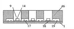
图1和图2示出了本发明检测细胞电信号装置的第一种实施方式的结构。该检测神经细胞电信号的装置包括微电极阵列传感器和细胞生长室。微电极阵列传感器包括基底1,在基底1上设有大微电极和小微电极;细胞生长室固定在基底1上。细胞生长室包括第一微室51、第二微室52、第三微室53和第一微通道7、第二微通道6。其中,第一微室51、第二微室52和第三微室53的上方均为敞口状。第一微室51、第二微室52和第三微室53平行排列。各微室之间通过腔壁46隔离。微电极阵列传感器上的大微电极对应地置于微室内,具体地说,可在第一微室51内沿着其长度方向a置有三个大微电极54,在第二微室52内沿着其长度a的方向置有三个大微电极55,在第三微室53内沿着其长度a的方向置有三个大微电极56。第一微室51内的大微电极和与第一微室51相邻的第二微室52内的大微电极之间对应地通过三个第一微通道7连通,第二微室52的大微电极和与第二微室52相邻的第三微室53的大微电极之间对应地通过三个第二微通道6连通。图1只示出了分别在第一微室51和第二微室52内且处于同一水平线上的大微电极之间由第一微通道7连通的结构形式。事实上,本发明可以通过第一微通道7将第一微室51内的任一大微电极与第二微室52内的任一大微电极连通,但各微通道之间不应交叉。同样,图1只示出了分别在第二微室52和第三微室53内且处于同一水平线上的大微电极之间由第二微通道6连通的结构形式。而本发明也可以通过第二微通道6将第二微室52内的任一大微电极与第三微室53内的任一大微电极连通,各微通道之间不交叉。微电极阵列传感器上的小微电极对应地置于微通道内,在各第一微通道7和第二微通道6内,沿着微通道长度c的方向,每个微通道内均可置有两个小微电极3。Figure 1 and Figure 2 show the structure of the first embodiment of the device for detecting cell electrical signals of the present invention. The device for detecting electrical signals of nerve cells includes a micro-electrode array sensor and a cell growth chamber. The microelectrode array sensor includes a
各第一微通道7和各第二微通道6的宽度d为仅够容纳一条神经突触。这样做的目的是:一条神经突触上的电信号仅被一个微通道中的小微电极检测到,一个微通道中的小微电极仅能检测到一条神经突触的电信号,从而使得微通道中的小微电极检测到的电信号与神经突触形成一一对应关系。The width d of each
小微电极3的直径与所要检测的神经突触的直径相等或者略小于神经突触直径,这是为了既使小微电极能构完全位于微通道中,又能检测到神经突触的电信号。否则,若小微电极过小,会导致小微电极与神经突触可能不接触,从而检测不到神经突触的电信号。The diameter of the
大微电极的直径约为所要检测的神经细胞的直径,这样做的目的是:既使大微电极能构完全位于微室中,又能检测到神经细胞的电信号。否则,若大微电极过小,只能检测到神经细胞部分表面上的电信号。The diameter of the large microelectrode is about the diameter of the nerve cell to be detected, and the purpose of doing this is: the electric signal of the nerve cell can be detected even if the large microelectrode can be completely located in the microchamber. Otherwise, if the large microelectrode is too small, only the electrical signal on the surface of part of the nerve cell can be detected.
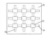
图3和图4示出了本发明检测细胞电信号装置的第二种实施方式的结构。该检测神经细胞电信号的装置包括微电极阵列传感器和细胞生长室。微电极阵列传感器包括基底1,在基底1上设有大微电极和小微电极;细胞生长室固定在基底1上。在该实施方式中,细胞生长室包括九个微室和二十四个微通道,九个微室在基底1上排列成三排三列的阵列,其中每个微室的上方均为敞口。微室之间通过腔壁46隔离。相邻的两个微室之间通过一个微通道连通。具体地说,例如,第一微室10和第二微室11通过第一微通道15连通,第二微室11与第四微室12通过第二微通道16连通,第四微室12和第三微室9通过第三微通道17连通,第三微室9与第一微室10通过第四微通道14连通,其它微室之间的连接与此类似。除了图3已示出的微室之间微通道的连接方式外,本发明还可以选择在第一微室10和第四微室12之间连通有微通道,或者是在第三微室9和第二微室11之间连通有微通道(未在图中示出),但各微通道之间不应交叉。3 and 4 show the structure of the second embodiment of the device for detecting cell electrical signals of the present invention. The device for detecting electrical signals of nerve cells includes a micro-electrode array sensor and a cell growth chamber. The microelectrode array sensor includes a
如图3所示,微电极阵列传感器上的大微电极18对应地置于微室内,微电极阵列传感器上的小微电极19对应地置于微通道内。具体地说,每个微室内置有一个大微电极18,每个微通道内沿着长度e方向可置有两个小微电极19。As shown in FIG. 3 , the
每个微室的大小为仅容纳一个神经细胞。微室的大小可略大于一个神经细胞的大小,但不能过大,否则一些较短的神经突触可能伸不进微通道内。Each microchamber is sized to accommodate only one neuron. The size of the microchamber can be slightly larger than the size of a nerve cell, but it should not be too large, otherwise some short synapses may not be able to extend into the microchannel.
每个微通道的宽度f为仅容纳一条神经突触。这样做的目的是:一条神经突触上的电信号仅被一个微通道中的小微电极检测到,一个微通道中的小微电极仅能检测到一条神经突触的电信号,使得微通道中的小微电极检测到的电信号与神经突触形成一一对应关系。The width f of each microchannel is such that only one synapse can be accommodated. The purpose of doing this is: the electrical signal on a nerve synapse is only detected by the small microelectrode in a microchannel, and the small microelectrode in a microchannel can only detect the electrical signal of a nerve synapse, so that the microchannel The electrical signals detected by the small microelectrodes in the sensor form a one-to-one correspondence with the synapses.
大微电极18的直径约为所要检测的神经细胞的直径,这样做的目的是:既使大微电极18能构完全位于微室中,又能检测到神经细胞的电信号,否则,若大微电极18过小,只能检测到神经细胞部分表面上的电信号。The diameter of
小微电极19的直径与所要检测的神经突触的直径相等或者略小于神经突触直径,这是为了既使小微电极能构完全位于微通道中,又能检测到神经突触的电信号,否则,若小微电极过小,会导致小微电极与神经突触可能不接触,从而检测不到神经突触的电信号。The diameter of the
以上是本发明的两种实施方式,在应用中,可根据所要检测的细胞的数量设置微室的数量;根据生物体中不同的神经细胞排列和连接的方式设置微室和微通道的排列方式,从而在本发明装置上培养的神经细胞的连接方式可以模拟生物体中的神经细胞的连接方式,因此培养在本装置上的神经细胞的电信号与生物体中的神经细胞的电信号类似,测到的电信号携带了更多生物学信息;也可以按照想要创造的人工神经网络的连接方式设置微室与微通道的排列方式,从而本装置上培养的细胞就会连接成想要的人工神经网络,通过MEA的微电极检测得到人工神经网络的电信号。The above are two embodiments of the present invention. In application, the number of microchambers can be set according to the number of cells to be detected; the arrangement of microchambers and microchannels can be set according to the arrangement and connection of different nerve cells in the organism , so that the connection mode of the nerve cells cultured on the device of the present invention can simulate the connection mode of the nerve cells in the organism, so the electrical signal of the nerve cells cultured on the device is similar to the electrical signal of the nerve cells in the organism, The measured electrical signal carries more biological information; the arrangement of microchambers and microchannels can also be set according to the connection method of the artificial neural network you want to create, so that the cells cultured on this device will be connected into the desired Artificial neural network, the electrical signal of the artificial neural network is obtained through the detection of the micro-electrodes of the MEA.
下面给出本发明第二种实施方式的制备方法。The preparation method of the second embodiment of the present invention is given below.
一、细胞生长室的制备1. Preparation of cell growth chamber
(1)用CAD软件设计出需要的图案,如图5所示,制作出有微通道图案23的掩膜20。(1) Design required pattern with CAD software, as shown in Figure 5, make the
(2)硅基底准备。将硅片放入Piranha溶液(16%浓硫酸∶30%双氧水=7∶3)煮沸清洗15min,用去离子水冲洗5遍后用氮气吹干,并在200℃热板上烘焙30min,如图6所示,制成硅基底22。(2) Silicon substrate preparation. Put the silicon wafer into Piranha solution (16% concentrated sulfuric acid: 30% hydrogen peroxide = 7:3) and boil it for 15 minutes, rinse it with deionized water for 5 times, blow it dry with nitrogen, and bake it on a hot plate at 200°C for 30 minutes, as shown in the figure 6, a
(3)甩涂。甩涂第一层光刻胶21,如图6所示,将光刻胶:SU-8 5胶21倒在硅基底22中央,用手握住硅片边缘使之倾斜并缓慢旋转,使SU-8 5胶21覆盖住硅基底22大部分区域。静置15min,使SU-8 5胶21初步平坦化,同时消除掉倾倒过程中产生的气泡。用旋涂机以4000rpm的速度甩涂60秒,使胶分布较为均匀,厚度大约为3μm,静置10min。(3) Spray coating. Spin and coat the first layer of
(4)软烘。将甩涂有光刻胶21的硅基底22放在热板上,以5℃/min的速率由室温逐步升到13℃,期间在65℃和13℃分别保持3min和6min。之后以0.5℃/min的速率缓慢降至室温。(4) Soft drying. Place the
(5)曝光。将刻有图案23的第一层掩膜20覆盖在光刻胶21的表面,如图6所示,然后曝光。采用I线接触式曝光机(波长365nm)。如图7所示,制作出光刻胶微通道24模具。光刻胶21在曝光后留下的部分即形成光刻胶微通道24。(5) Exposure. Cover the surface of the
(6)PEB(Post Exposure Bake,曝光后烘)烘焙。将上述模具置于热板上,以5℃/min的速率由室温逐步升到13℃,期间在65℃和13℃分别保持1min和5min。之后以0.5℃/min的速率缓慢降至室温。(6) PEB (Post Exposure Bake, post-exposure baking) baking. Place the mold above on a hot plate, and gradually raise it from room temperature to 13°C at a rate of 5°C/min, and keep at 65°C and 13°C for 1 min and 5 min, respectively. Then slowly lower to room temperature at a rate of 0.5°C/min.
(7)制作掩膜。用CAD软件设计出需要的图案,制作出微室的掩膜。(7) Make a mask. Use CAD software to design the required pattern and make the mask of the microchamber.
(8)甩涂第二层光刻胶。SU-8 50光刻胶作为第二层光刻胶,以1000rpm的速度在有微通道的硅基底上甩涂60秒。(8) Spin and coat the second layer of photoresist. SU-8 50 photoresist was used as the second layer of photoresist, and was spin-coated on the silicon substrate with microchannels for 60 seconds at a speed of 1000 rpm.
(9)软烘。(9) Soft drying.
(10)曝光。将刻有微室图案的第二层掩膜与第一层光刻图形对准,第二次曝光,如图8所示,制作出光刻胶微室25模具。由于第一层光刻胶和第二层光刻胶的材料不同,调整曝光时间和光源波长,可保证此次曝光不损坏已经制作出的微通道。(10) EXPOSURE. Align the second-layer mask engraved with the micro-chamber pattern with the first-layer photolithographic pattern, and expose for the second time, as shown in FIG. 8 , to make a
(11)PEB(Post Exposure Bake,曝光后烘)烘焙。将上述光刻胶模具进行PEB烘焙,具体方法同步骤6。(11) PEB (Post Exposure Bake, post-exposure baking) baking. The above-mentioned photoresist mold is subjected to PEB baking, and the specific method is the same as
(12)显影。显影在通风橱中进行,显影液的主要成分是PGMEA。在光刻胶模具与显影液分别静置达到室温后,将模具放入显影液中显影6min,光刻胶的非感光区溶解于显影液中,之后分别用异丙醇和去离子水清洗干净,并用氮气吹干。(12) Development. The development was carried out in a fume hood, and the main component of the developer was PGMEA. After the photoresist mold and the developer were left to stand at room temperature, the mold was put into the developer for 6 minutes to develop, and the non-photosensitive area of the photoresist was dissolved in the developer, and then cleaned with isopropanol and deionized water respectively. and blow dry with nitrogen.
(13)硬烘。将上述光刻胶模具置于热板上,缓慢加热到200℃,保持30min,再缓慢降温至室温。(13) Hard baking. The above photoresist mold was placed on a hot plate, slowly heated to 200° C., kept for 30 min, and then slowly cooled to room temperature.
(14)PDMS浇注。按照PDMS预聚体(Sylgard184硅橡胶)和PDMS固化剂(3-环氧丙氧丙基三甲氧基硅烷)的比例为10∶1,称量PDMS预聚体6.5克,PDMS固化剂0.65克置于试管中,混合均匀。分别用低真空抽30分钟,高真空抽15分钟,至无气泡生成为止。将混合液体缓慢浇注于光刻胶模具上,在70℃的环境下静置一小时使之固化,形成如图9所示的PDMS腔壁46,腔壁46中有光刻胶微室24和光刻胶微通道25。(14) PDMS casting. According to the ratio of PDMS prepolymer (Sylgard184 silicone rubber) and PDMS curing agent (3-glycidoxypropyltrimethoxysilane) is 10:1, weigh 6.5 grams of PDMS prepolymer, and place 0.65 grams of PDMS curing agent In a test tube, mix well. Use low vacuum for 30 minutes and high vacuum for 15 minutes, until no bubbles are formed. Slowly pour the mixed liquid on the photoresist mold, and let it stand for one hour in an environment of 70° C. to solidify, forming a
(15)脱模处理。将上述PDMS腔壁从光刻胶模具上剥离,这样,光刻胶模具上的图案就完好地转移到PDMS腔壁上,在PDMS腔壁中形成了微室和微通道,如图10。沿着图10虚线处切割PDMS腔壁,使微室的开口暴露出来,成为敞口的微室,即形成细胞生长室,“敞口”的目的是为了细胞可以放入。(15) Release treatment. The above-mentioned PDMS cavity wall was peeled off from the photoresist mold, so that the pattern on the photoresist mold was transferred to the PDMS cavity wall intact, and microchambers and microchannels were formed in the PDMS cavity wall, as shown in Figure 10. Cut the wall of the PDMS cavity along the dotted line in Figure 10 to expose the opening of the microchamber and become an open microchamber, that is, to form a cell growth chamber. The purpose of the "opening" is for cells to enter.
二、定制的MEA2. Customized MEA
电极的位点和大小如图11和图12所示。大微电极18和小微电极19的排列方式对应微室和微通道的排列方式。The location and size of the electrodes are shown in Figure 11 and Figure 12. The arrangement of the
三、细胞生长室与MEA的封装3. Encapsulation of cell growth chamber and MEA
将MEA水平放置,将细胞生长室的下端粘合在MEA的基底1表面,封装过程中要保证微室和微通道覆盖微电极阵列传感器上的对应电极。覆盖是指电极完全位于微室或微通道的下方而没有暴露出来。最终完成品如图3和图4。Place the MEA horizontally, glue the lower end of the cell growth chamber to the surface of the
四、本发明装置的工作过程Four, the working process of the device of the present invention
将不同的神经细胞培养在不同的微室内的大微电极上,几天以后每个细胞的突触将沿着微通道生长,在微通道内连接起来,形成了定向生长的神经网络,这时可以通过微电极将神经细胞电信号检测出来。Different nerve cells are cultured on large microelectrodes in different microchambers. After a few days, the synapses of each cell will grow along the microchannel and connect in the microchannel to form a directional growth neural network. At this time The electrical signals of nerve cells can be detected by microelectrodes.
Claims (3)
Translated fromChinesePriority Applications (1)
| Application Number | Priority Date | Filing Date | Title |
|---|---|---|---|
| CN 200910100987CN101629945B (en) | 2009-08-06 | 2009-08-06 | Device for detecting electrical signal of nerve cell |
Applications Claiming Priority (1)
| Application Number | Priority Date | Filing Date | Title |
|---|---|---|---|
| CN 200910100987CN101629945B (en) | 2009-08-06 | 2009-08-06 | Device for detecting electrical signal of nerve cell |
Publications (2)
| Publication Number | Publication Date |
|---|---|
| CN101629945A CN101629945A (en) | 2010-01-20 |
| CN101629945Btrue CN101629945B (en) | 2012-11-14 |
Family
ID=41575126
Family Applications (1)
| Application Number | Title | Priority Date | Filing Date |
|---|---|---|---|
| CN 200910100987Expired - Fee RelatedCN101629945B (en) | 2009-08-06 | 2009-08-06 | Device for detecting electrical signal of nerve cell |
Country Status (1)
| Country | Link |
|---|---|
| CN (1) | CN101629945B (en) |
Families Citing this family (6)
| Publication number | Priority date | Publication date | Assignee | Title |
|---|---|---|---|---|
| CN103901089B (en)* | 2014-04-16 | 2016-08-24 | 国家纳米科学中心 | The detection sensor of neurocyte electricity physiological signal and manufacture method and detection method |
| CN107758605B (en)* | 2016-08-16 | 2020-01-31 | 中国科学院上海微系统与信息技术研究所 | Microelectrode array chip and method of making the same |
| CN110955041A (en)* | 2020-01-10 | 2020-04-03 | 太原理工大学 | An all-solid-state variable-focus piezoelectric actuated microlens based on SEBS film |
| CN112111455B (en)* | 2020-09-27 | 2022-04-22 | 北京理工大学 | An in vitro artificial reflex arc-like structure and its construction method and application |
| TWI854167B (en)* | 2020-12-14 | 2024-09-01 | 國立中央大學 | Integrated microfluidic chip for cell imaging and biochemical detection and method using the same |
| CN113684133B (en)* | 2021-09-09 | 2023-11-24 | 中国科学院空天信息创新研究院 | A neuron NOT gate logic functional chip integrating microfluidics and microelectrode array and its preparation method |
Citations (1)
| Publication number | Priority date | Publication date | Assignee | Title |
|---|---|---|---|---|
| CN201488996U (en)* | 2009-08-06 | 2010-05-26 | 浙江大学 | A device for detecting electrical signals of nerve cells |
- 2009
- 2009-08-06CNCN 200910100987patent/CN101629945B/ennot_activeExpired - Fee Related
Patent Citations (1)
| Publication number | Priority date | Publication date | Assignee | Title |
|---|---|---|---|---|
| CN201488996U (en)* | 2009-08-06 | 2010-05-26 | 浙江大学 | A device for detecting electrical signals of nerve cells |
Also Published As
| Publication number | Publication date |
|---|---|
| CN101629945A (en) | 2010-01-20 |
Similar Documents
| Publication | Publication Date | Title |
|---|---|---|
| CN101629945B (en) | Device for detecting electrical signal of nerve cell | |
| CN102156158B (en) | Device for culturing and measuring microfluidic chip by using topological diagram type nerve cell network | |
| CN104760922B (en) | A kind of ultra micro planar electrode array sensor and preparation method thereof | |
| Hällström et al. | Gallium phosphide nanowires as a substrate for cultured neurons | |
| CN105925480B (en) | Micro-fluidic chip and preparation method for blood-brain barrier drug permeability high flux screening | |
| Claverol-Tinture et al. | Multielectrode arrays with elastomeric microstructured overlays for extracellular recordings from patterned neurons | |
| CN109894163B (en) | High-flux and high-content drug screening micro-fluidic chip and preparation method thereof | |
| Kang et al. | Agarose microwell based neuronal micro-circuit arrays on microelectrode arrays for high throughput drug testing | |
| CN201488996U (en) | A device for detecting electrical signals of nerve cells | |
| CN107118938A (en) | The unicellular arrangement of fluid enhancing dielectrophoresis and control chip and preparation method thereof | |
| CN113684133B (en) | A neuron NOT gate logic functional chip integrating microfluidics and microelectrode array and its preparation method | |
| CN115109699A (en) | Organ chip with integrated microelectrode array and method of making and using the same | |
| CN115216405A (en) | Multilayer cascade neural network micro-fluidic chip and preparation method thereof | |
| CN105460882A (en) | Graphene three-dimensional microelectrode array chip, and method and application thereof | |
| JP4370082B2 (en) | Neuron culture microchamber | |
| CN101748061B (en) | Device and method for growing connections between neurons at the single-cell level | |
| CN103630583A (en) | Multizone multifunctional nerve dual-mode detection microelectrode array chip and preparation method | |
| CN107907485B (en) | Heart chip based on structural color hydrogel and application thereof | |
| CN102337211A (en) | Cell culture device | |
| CN116237099A (en) | Microfluidic chip for in situ electrical impedance spectroscopy detection of nematodes | |
| Hammack et al. | A patterned polystyrene-based microelectrode array for in vitro neuronal recordings | |
| US20070231850A1 (en) | Patterned Cell Network Substrate Interface and Methods and Uses Thereof | |
| CN103344903B (en) | A kind of neuro chip measurement mechanism of high-spatial and temporal resolution | |
| CN117363481A (en) | Microfluidic neural chip for realizing single-cell electrical interconnection, preparation method and inspection method | |
| CN106732842B (en) | For the micro-fluidic chip and preparation method thereof without mark high content screening |
Legal Events
| Date | Code | Title | Description |
|---|---|---|---|
| C06 | Publication | ||
| PB01 | Publication | ||
| C10 | Entry into substantive examination | ||
| SE01 | Entry into force of request for substantive examination | ||
| C14 | Grant of patent or utility model | ||
| GR01 | Patent grant | ||
| CF01 | Termination of patent right due to non-payment of annual fee | Granted publication date:20121114 Termination date:20190806 | |
| CF01 | Termination of patent right due to non-payment of annual fee |