CN101620328B - Touch LCD screen - Google Patents
Touch LCD screenDownload PDFInfo
- Publication number
- CN101620328B CN101620328BCN2008100683173ACN200810068317ACN101620328BCN 101620328 BCN101620328 BCN 101620328BCN 2008100683173 ACN2008100683173 ACN 2008100683173ACN 200810068317 ACN200810068317 ACN 200810068317ACN 101620328 BCN101620328 BCN 101620328B
- Authority
- CN
- China
- Prior art keywords
- layer
- carbon nanotube
- liquid crystal
- touch
- crystal display
- Prior art date
- Legal status (The legal status is an assumption and is not a legal conclusion. Google has not performed a legal analysis and makes no representation as to the accuracy of the status listed.)
- Expired - Fee Related
Links
Images


Landscapes
- Liquid Crystal (AREA)
- Devices For Indicating Variable Information By Combining Individual Elements (AREA)
Abstract
Translated fromChinese
Description
Translated fromChinese技术领域technical field
本发明涉及一种液晶显示屏,尤其涉及一种触摸式液晶显示屏。The invention relates to a liquid crystal display screen, in particular to a touch type liquid crystal display screen.
背景技术Background technique
液晶显示因为低功耗、小型化及高质量的显示效果,成为最佳的显示方式之一。目前较为常用的液晶显示屏为TN(扭曲向列相)模式的液晶显示屏(TN-LCD)。对于TN-LCD,当电极上未施加电压时,液晶显示屏处于“OFF”状态,光能透过液晶显示屏呈通光状态;当在电极上施加一定电压时,液晶显示屏处于“ON”态,液晶分子长轴方向沿电场方向排列,光不能透过液晶显示屏,故呈遮光状态。有选择地在电极上施加电压,可以显示出不同的图案。Liquid crystal display has become one of the best display methods because of low power consumption, miniaturization and high-quality display effect. Currently, the more commonly used liquid crystal display is a TN (twisted nematic) mode liquid crystal display (TN-LCD). For TN-LCD, when no voltage is applied to the electrodes, the liquid crystal display is in the "OFF" state, and the light energy passes through the liquid crystal display in a light-transmitting state; when a certain voltage is applied to the electrodes, the liquid crystal display is in the "ON" state In the state, the long axis direction of the liquid crystal molecules is arranged along the direction of the electric field, and the light cannot pass through the liquid crystal display, so it is in a light-shielding state. By selectively applying a voltage across the electrodes, different patterns can be displayed.
近年来,伴随着移动电话、触摸导航系统、集成式电脑显示器及互动电视等各种电子设备的高性能化和多样化的发展,在液晶显示屏的显示面安装透光性的触摸屏的电子设备逐渐增加。电子设备的使用者通过触摸屏,一边对位于触摸屏背面的液晶显示屏的显示内容进行视觉确认,一边利用手指或笔等方式按压触摸屏来进行操作。由此,可以操作使用该液晶显示屏的电子设备的各种功能。In recent years, with the high-performance and diversified development of various electronic devices such as mobile phones, touch navigation systems, integrated computer monitors, and interactive TVs, electronic devices that install light-transmitting touch screens on the display surface of liquid crystal displays gradually increase. The user of the electronic device uses the touch screen to visually confirm the display content of the liquid crystal display located on the back of the touch screen, and at the same time presses the touch screen with a finger or a pen to perform operations. Thereby, various functions of electronic equipment using the liquid crystal display can be operated.
所述触摸屏可根据其工作原理和传输介质的不同,通常分为四种类型,分别为电阻式、电容感应式、红外线式以及表面声波式。其中电阻式触摸屏由于其具有高分辨率、高灵敏度及耐用等优点被广泛应用。The touch screen can be generally divided into four types according to its working principle and transmission medium, namely resistive type, capacitive sensing type, infrared type and surface acoustic wave type. Among them, the resistive touch screen is widely used due to its advantages of high resolution, high sensitivity and durability.
然而,现有技术中的电阻式触摸屏通常包括一个铟锡氧化物层(ITO层)作为透明导电层,其采用离子束溅射或蒸镀等工艺制备,Kazuhiro Noda等在文献Production of Transparent Conductive Films with Inserted SiO2 AnchorLayer,and Application to a Resistive Touch Panel(Electronics andCommunications in Japan,Part 2,Vol.84,P39-45(2001))中介绍了一种采用ITO/SiO2/聚对苯二甲酸乙二醇酯层的触摸屏。该ITO层在制备的过程,需要较高的真空环境及需要加热到200~300℃,因此,使得采用ITO作为透明导电层的触摸屏的制备成本较高。此外,现有技术中的ITO层作为透明导电层具有机械性能不够好、难以弯曲及阻值分布不均匀等缺点,不适用于柔性的触摸式液晶显示屏中。另外,ITO在潮湿的空气中透明度会逐渐下降。从而导致现有的触摸屏及使用该触摸屏的触摸式液晶显示屏在耐用性不够好,灵敏度低、线性及准确性较差等缺点。However, the resistive touch screen in the prior art usually includes an indium tin oxide layer (ITO layer) as a transparent conductive layer, which is prepared by ion beam sputtering or evaporation, Kazuhiro Noda et al. in the literature Production of Transparent Conductive Films with Inserted SiO2 AnchorLayer, and Application to a Resistive Touch Panel (Electronics and Communications in Japan, Part 2, Vol.84, P39-45 (2001)) introduces a method using ITO/SiO2 /polyethylene terephthalate Touch screen with glycol ester layer. During the preparation process of the ITO layer, a relatively high vacuum environment is required and heating to 200-300° C. is required. Therefore, the preparation cost of the touch screen using ITO as the transparent conductive layer is relatively high. In addition, as a transparent conductive layer, the ITO layer in the prior art has disadvantages such as insufficient mechanical properties, difficulty in bending, and uneven resistance distribution, and is not suitable for flexible touch-type liquid crystal displays. In addition, the transparency of ITO will gradually decrease in humid air. As a result, the existing touch screen and the touch-type liquid crystal display using the touch screen have disadvantages such as insufficient durability, low sensitivity, poor linearity and accuracy.
有鉴于此,确有必要提供一种触摸式液晶显示屏,该触摸式液晶显示屏具有耐用性好、灵敏度高、线性及准确性强的优点。In view of this, it is indeed necessary to provide a touch-type liquid crystal display, which has the advantages of good durability, high sensitivity, strong linearity and high accuracy.
发明内容Contents of the invention
一种触摸式液晶显示屏,其包括一上基板、一下基板以及一液晶层,该上基板包括一触摸屏,该下基板与上基板相对设置,该下基板包括一薄膜晶体管面板,该液晶层设置于该上基板与下基板之间,其中,该触摸屏中的导电层包括一第一碳纳米管层,该薄膜晶体管面板中的薄膜晶体管的半导体层包括一第二碳纳米管层。A touch-type liquid crystal display, which includes an upper substrate, a lower substrate and a liquid crystal layer, the upper substrate includes a touch screen, the lower substrate is arranged opposite to the upper substrate, the lower substrate includes a thin film transistor panel, and the liquid crystal layer is set Between the upper substrate and the lower substrate, the conductive layer in the touch screen includes a first carbon nanotube layer, and the semiconductor layer of the thin film transistor in the thin film transistor panel includes a second carbon nanotube layer.
与现有技术相比较,所述触摸式液晶显示屏具有以下优点:其一,由于采用碳纳米管的触摸屏可直接输入操作命令和信息,可代替传统的键盘、鼠标或按键等输入设备,从而可以简化使用该触摸式液晶显示屏的电子设备的结构。其二,碳纳米管的优异的力学特性使得透明导电层具有很好的韧性和机械强度,并且耐弯折,故,可以相应的提高触摸屏的耐用性,进而提高该触摸式液晶显示屏的耐用性,同时,与柔性基体配合,可以制备一柔性触摸式液晶显示屏。另外,采用半导体性碳纳米管层代替现有的非晶硅、多晶硅或有机半导体聚合物作为半导体层,可以相应的提高薄膜晶体管的柔性,尤其适用于柔性薄膜晶体管面板,并应用于柔性触摸式液晶显示屏中。其三,由于碳纳米管在潮湿的条件下具有良好的透明度,故采用碳纳米管层作为触摸屏的透明导电层,可以使该触摸屏具有较好的透明度,进而有利于提高该触摸式液晶显示屏的分辨率。其四,由于碳纳米管具有优异的导电性能,则由碳纳米管组成的碳纳米管层具有均匀的阻值分布,因而,采用上述碳纳米管层作透明导电层,可以相应的提高触摸屏的分辨率和精确度,进而提高该触摸式液晶显示屏的分辨率和精确度。其五,由于半导体性的碳纳米管具有优异的半导体性,因此薄膜晶体管具有较大的载流子迁移率,薄膜晶体管面板具有较快的响应速率,从而使应用该薄膜晶体管面板的触摸式液晶显示屏具有较好的显示性能。其六,采用碳纳米管层作为半导体层的薄膜晶体管尺寸较小,薄膜晶体管面板分辨率更高,可以用于提高触摸式液晶显示屏的分辨率。Compared with the prior art, the touch-type liquid crystal display has the following advantages: First, because the touch screen using carbon nanotubes can directly input operation commands and information, it can replace traditional input devices such as keyboards, mice or buttons, thereby The structure of electronic equipment using the touch-type liquid crystal display can be simplified. Second, the excellent mechanical properties of carbon nanotubes make the transparent conductive layer have good toughness and mechanical strength, and are resistant to bending. Therefore, the durability of the touch screen can be correspondingly improved, thereby improving the durability of the touch-type liquid crystal display. At the same time, a flexible touch-type liquid crystal display can be prepared by cooperating with a flexible substrate. In addition, the use of semiconducting carbon nanotube layers instead of the existing amorphous silicon, polysilicon or organic semiconducting polymers as semiconductor layers can correspondingly improve the flexibility of thin film transistors, especially suitable for flexible thin film transistor panels, and applied to flexible touch in the LCD screen. Its three, because carbon nanotube has good transparency under humid condition, so adopt carbon nanotube layer as the transparent conductive layer of touch screen, can make this touch screen have good transparency, and then help to improve this touch-type liquid crystal display screen. resolution. Its four, because carbon nanotube has excellent electrical conductivity, then the carbon nanotube layer that is made up of carbon nanotube has uniform resistance value distribution, thereby, adopt above-mentioned carbon nanotube layer to make transparent conductive layer, can correspondingly improve the touch screen. Resolution and accuracy, thereby improving the resolution and accuracy of the touch LCD display. Fifth, due to the excellent semiconductor properties of semiconducting carbon nanotubes, thin film transistors have greater carrier mobility, and thin film transistor panels have faster response rates, so that touch-type liquid crystals using the thin film transistor panels The display screen has better display performance. Sixth, the size of the thin film transistor using the carbon nanotube layer as the semiconductor layer is small, and the resolution of the thin film transistor panel is higher, which can be used to improve the resolution of the touch-type liquid crystal display.
附图说明Description of drawings
图1是本技术方案实施例触摸式液晶显示屏的侧视结构示意图。Fig. 1 is a schematic diagram of a side view structure of a touch-type liquid crystal display according to an embodiment of the technical solution.
图2是本技术方案实施例触摸式液晶显示屏中上基板的立体结构示意图。Fig. 2 is a schematic diagram of the three-dimensional structure of the upper substrate in the touch-type liquid crystal display of the embodiment of the technical solution.
图3是本技术方案实施例触摸式液晶显示屏中下基板的立体结构示意图。Fig. 3 is a schematic diagram of the three-dimensional structure of the lower substrate in the touch-type liquid crystal display of the embodiment of the technical solution.
图4是本技术方案实施例触摸式液晶显示屏中碳纳米管拉膜结构的扫描电镜照片。Fig. 4 is a scanning electron microscope photo of the carbon nanotube stretched film structure in the touch-type liquid crystal display of the embodiment of the technical solution.
图5是本技术方案实施例触摸式液晶显示屏中薄膜晶体管面板的俯视结构示意图。FIG. 5 is a schematic top view of a thin film transistor panel in a touch-type liquid crystal display according to an embodiment of the technical solution.
图6是图5的薄膜晶体管面板中薄膜晶体管的剖视图。FIG. 6 is a cross-sectional view of a thin film transistor in the thin film transistor panel of FIG. 5 .
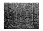
图7是图6的薄膜晶体管中的长碳纳米管薄膜结构的扫描电镜照片。FIG. 7 is a scanning electron micrograph of the long carbon nanotube film structure in the thin film transistor of FIG. 6 .
图8是本技术方案实施例触摸式液晶显示屏工作原理的示意图。Fig. 8 is a schematic diagram of the working principle of the touch-type LCD according to the embodiment of the technical solution.
具体实施方式Detailed ways
以下将结合附图详细说明本技术方案的触摸式液晶显示屏。The touch-type liquid crystal display screen of the technical solution will be described in detail below in conjunction with the accompanying drawings.
请参阅图1,本技术方案实施例提供一种触摸式液晶显示屏300,其包括一上基板100、一与上基板100相对设置的下基板200以及一设置于该上基板100与下基板200之间的液晶层310。Please refer to FIG. 1 , the embodiment of the technical solution provides a touch-type
所述液晶层310包括多个长棒状的液晶分子。所述液晶层310的液晶材料为现有技术中常用的液晶材料。所述液晶层310的厚度1~50微米,本实施例中,液晶层310的厚度为5微米。The
请参阅图2,所述上基板100从上至下依次包括一触摸屏10、一第一偏光层110及一第一配向层112。该第一偏光层110设置于该触摸屏10的下表面,用于控制通过液晶层310的偏振光的出射。该第一配向层112设置于所述第一偏光层110的下表面。进一步地,该第一配向层112的下表面包括多个平行的第一沟槽,用于使液晶层310的液晶分子定向排列。该上基板100中第一配向层112靠近液晶层310设置。Please refer to FIG. 2 , the
该触摸屏10为四线、五线或八线式结构的电阻式触摸屏。本实施例中,该触摸屏10为四线式结构,其从上至下依次包括一第一电极板12、多个透明的点状隔离物16及一第二电极板14。该第二电极板14与第一电极板12相对设置,该多个透明的点状隔离物16设置在第一电极板12与第二电极板14之间。The
该第一电极板12包括一第一基体120,一第一导电层122以及两个第一电极124。该第一基体120为平面结构,该第一导电层122与两个第一电极124均设置在第一基体120的下表面。两个第一电极124分别设置在第一导电层122沿第一方向的两端并与第一导电层122电连接。该第二电极板14包括一第二基体140,一第二导电层142以及两个第二电极144。该第二基体140为平面结构,该第二导电层142与两个第二电极144均设置在第二基体140的上表面。两个第二电极144分别设置在第二导电层142沿第二方向的两端并与第二导电层142电连接。其中第一方向垂直于第二方向,即两个第一电极124与两个第二电极144正交设置。The
所述触摸屏10的第一基体120与第二基体140均为透明的薄膜或薄板。该第一基体120具有一定柔软度,可由塑料或树脂等柔性材料形成。该第二基体140的材料可以为玻璃、石英、金刚石等硬性材料。当用于柔性触摸式液晶显示屏300中时,该第二基体140的材料也可为塑料或树脂等柔性材料。具体地,该第一基体120及第二基体140所用的材料可以为聚碳酸酯(PC)、聚甲基丙烯酸甲酯(PMMA)、聚对苯二甲酸乙二醇酯(PET)等聚酯材料,以及聚醚砜(PES)、纤维素酯、聚氯乙烯(PVC)、苯并环丁烯(BCB)及丙烯酸树脂等材料。该第一基体120和第二基体140的厚度为1毫米~1厘米。本实施例中,该第一基体120及第二基体140的材料均为PET,厚度均为2毫米。可以理解,形成所述第一基体120及第二基体140的材料并不限于上述列举的材料,只要能使第一基体120及第二基体140起到支撑的作用,并具有较好的透明度,且至少形成第一基体120的材料具有一定柔性,都在本发明保护的范围内。Both the
所述触摸屏10的第一导电层122与第二导电层142均包括一第一碳纳米管层,该碳纳米管层包括多个金属性碳纳米管。进一步地,上述的碳纳米管层可以是单个碳纳米管薄膜或是多个平行无间隙铺设的碳纳米管薄膜。可以理解,由于上述的碳纳米管层中的多个碳纳米管薄膜可以平行且无间隙的铺设,故,上述碳纳米管层的长度和宽度不限,可根据实际需要制成具有任意长度和宽度的碳纳米管层。另外,上述碳纳米管层中可进一步包括多个碳纳米管薄膜重叠设置,故,上述碳纳米管层的厚度也不限,只要能够具有理想的透明度,可根据实际需要制成具有任意厚度的碳纳米管层。Both the first
上述碳纳米管层中的碳纳米管薄膜由有序的或无序的碳纳米管组成,并且该碳纳米管薄膜具有均匀的厚度。具体地,该碳纳米管层包括无序的碳纳米管薄膜或者有序的碳纳米管薄膜。无序的碳纳米管薄膜中,碳纳米管为无序或各向同性排列。该无序排列的碳纳米管相互缠绕,该各向同性排列的碳纳米管平行于碳纳米管薄膜的表面。有序的碳纳米管薄膜中,碳纳米管为沿同一方向择优取向排列或沿不同方向择优取向。当碳纳米管层包括多层有序碳纳米管薄膜时,该多层碳纳米管薄膜可以沿任意方向重叠设置,因此,在该碳纳米管层中,碳纳米管为沿相同或不同方向择优取向排列。优选地,当该碳纳米管层中的碳纳米管薄膜为有序碳纳米管薄膜时,该有序碳纳米管薄膜为从碳纳米管阵列中直接拉取获得的碳纳米管拉膜结构。请参阅图4,所述碳纳米管拉膜结构包括多个碳纳米管首尾相连且择优取向排列。该多个碳纳米管之间通过范德华力结合。一方面,首尾相连的碳纳米管之间通过范德华力连接;另一方面,择优取向排列的碳纳米管之间部分通过范德华力结合。故,该碳纳米管拉膜结构具有较好的自支撑性及柔韧性。当该碳纳米管层中包括多层重叠设置的碳纳米管拉膜结构时,相邻两层碳纳米管薄膜中碳纳米管形成一夹角α,且0°≤α≤90°。The carbon nanotube film in the carbon nanotube layer is composed of ordered or disordered carbon nanotubes, and the carbon nanotube film has a uniform thickness. Specifically, the carbon nanotube layer includes a disordered carbon nanotube film or an ordered carbon nanotube film. In the disordered carbon nanotube film, the carbon nanotubes are arranged in a disordered or isotropic manner. The disorderly arranged carbon nanotubes are intertwined, and the isotropic arranged carbon nanotubes are parallel to the surface of the carbon nanotube film. In the ordered carbon nanotube film, the carbon nanotubes are preferentially oriented in the same direction or preferentially oriented in different directions. When the carbon nanotube layer includes a multi-layer ordered carbon nanotube film, the multi-layer carbon nanotube film can be stacked in any direction, therefore, in the carbon nanotube layer, the carbon nanotubes are preferentially arranged along the same or different directions. alignment. Preferably, when the carbon nanotube film in the carbon nanotube layer is an ordered carbon nanotube film, the ordered carbon nanotube film is a carbon nanotube film structure obtained by directly pulling from the carbon nanotube array. Please refer to FIG. 4 , the carbon nanotube stretched film structure includes a plurality of carbon nanotubes connected end to end and arranged in a preferred orientation. The plurality of carbon nanotubes are bonded by van der Waals force. On the one hand, the end-to-end carbon nanotubes are connected by van der Waals force; on the other hand, the carbon nanotubes arranged in the preferred orientation are partially bonded by van der Waals force. Therefore, the carbon nanotube stretched film structure has better self-supporting property and flexibility. When the carbon nanotube layer includes a carbon nanotube stretched film structure stacked in multiple layers, the carbon nanotubes in two adjacent layers of carbon nanotube films form an included angle α, and 0°≤α≤90°.
进一步地,所述碳纳米管层可以包括上述各种碳纳米管薄膜与一高分子材料组成的复合薄膜。所述高分子材料均匀分布于所述碳纳米管薄膜中碳纳米管之间的间隙中。所述高分子材料为一透明高分子材料,其具体材料不限,包括聚苯乙烯、聚乙烯、聚碳酸酯、聚甲基丙烯酸甲酯(PMMA)、聚碳酸酯(PC)、对苯二甲酸乙二醇酯(PET)、苯丙环丁烯(BCB)、聚环烯烃等。Further, the carbon nanotube layer may include a composite film composed of the above-mentioned various carbon nanotube films and a polymer material. The polymer material is evenly distributed in the gaps between the carbon nanotubes in the carbon nanotube film. Described macromolecular material is a transparent macromolecular material, and its specific material is not limited, comprises polystyrene, polyethylene, polycarbonate, polymethyl methacrylate (PMMA), polycarbonate (PC), terephthalmic Ethylene glycol formate (PET), benzocyclobutene (BCB), polycycloolefin, etc.
本实施例中,所述第一导电层122与第二导电层142中的碳纳米管层为一层碳纳米管拉膜结构与PMMA组成的复合薄膜。具体的,第一导电层122的碳纳米管拉膜结构中碳纳米管均沿第一方向排列,第二导电层142的碳纳米管拉膜结构中碳纳米管均沿第二方向排列。所述碳纳米管复合薄膜的厚度为0.5纳米~100微米,宽度为0.01厘米~10厘米。In this embodiment, the carbon nanotube layer in the first
所述碳纳米管层中金属性碳纳米管包括单壁碳纳米管、双壁碳纳米管以及多壁碳纳米管中的一种或几种。所述单壁碳纳米管的直径为0.5纳米~50纳米,双壁碳纳米管的直径为1纳米~50纳米,多壁碳纳米管的直径为1.5纳米~50纳米。所述碳纳米管层的厚度为0.5纳米~100微米。The metallic carbon nanotubes in the carbon nanotube layer include one or more of single-wall carbon nanotubes, double-wall carbon nanotubes and multi-wall carbon nanotubes. The single-walled carbon nanotubes have a diameter of 0.5 nm to 50 nm, the double-walled carbon nanotubes have a diameter of 1 nm to 50 nm, and the multi-walled carbon nanotubes have a diameter of 1.5 nm to 50 nm. The carbon nanotube layer has a thickness of 0.5 nanometers to 100 micrometers.
所述触摸屏10的第一电极124与第二电极144由导电材料形成,具体可以选择为金属层、导电聚合物层或碳纳米管层。所述金属层的材料可以选择为金、银或铜等导电性好的金属。所述导电聚合物层的材料可以选择为聚乙炔、聚对苯撑、聚苯胺、聚咪吩、聚毗咯、聚噻吩等。优选的,该碳纳米管层包括至少一碳纳米管拉膜结构。本实施例中,该第一电极124与第二电极144为导电的银浆层。可以理解,用于柔性触摸式液晶显示屏300上的上述电极应具有一定的韧性和易弯折度。The
进一步地,在所述触摸屏10中,该第二电极板14靠近第一电极板12的表面外围设置有一绝缘层18。上述的第一电极板12设置在该绝缘层18上,且该第一电极板12的第一导电层122正对第二电极板14的第二导电层142设置。上述多个点状隔离物16设置在第二电极板14的第二导电层142上,且该多个点状隔离物16彼此间隔设置。第一电极板12与第二电极板14之间的距离为2~10微米。该绝缘层18与点状隔离物16均可采用绝缘树脂或其他绝缘材料制成,并且,该点状隔离物16应为一透明材料制成。设置绝缘层18与点状隔离物16可使得第一电极板14与第二电极板12电绝缘。可以理解,当触摸屏10尺寸较小时,点状隔离物16为可选择的结构,只需确保第一电极板14与第二电极板12电绝缘即可。Further, in the
另外,该第一电极板12远离第二电极板14的表面进一步可设置一透明保护膜126。所述透明保护膜126可以通过粘结剂直接粘结在第一基体120上表面,也可采用热压法,与第一电极板12压合在一起。该透明保护膜126可采用一层表面硬化处理、光滑防刮的塑料层或树脂层,该树脂层可由苯丙环丁烯(BCB)、聚酯以及丙烯酸树脂等材料形成。本实施例中,形成该透明保护膜126的材料为聚对苯二甲酸乙二醇酯(PET),用于保护第一电极板12,提高耐用性。该透明保护膜126可用以提供一些附加功能,如可以减少眩光或降低反射。In addition, a transparent
所述第一偏光层110的材料可以为现有技术中常用的偏光材料,如二向色性有机高分子材料,具体可以为碘系材料或染料材料等。另外,该第一偏光层110也可为一层有序的碳纳米管薄膜,所述有序的碳纳米管薄膜中碳纳米管沿同一方向定向排列。优选的,该第一偏光层110为一碳纳米管拉膜结构。所述第一第一偏光层110的厚度为1微米~0.5毫米。The material of the first
由于碳纳米管对电磁波的吸收接近绝对黑体,碳纳米管对于各种波长的电磁波均有均一的吸收特性,故所述第一偏光层110中的有序碳纳米管薄膜对于各种波长的电磁波也有均一的偏振吸收性能。当光波入射时,振动方向平行于碳纳米管束长度方向的光被吸收,垂直于碳纳米管束长度方向的光能透过,所以透射光成为线偏振光。因此,碳纳米管薄膜可以代替现有技术中的偏振片起到偏光作用。另外,所述第一偏光层110包括沿同一方向定向排列的碳纳米管,从而所述所述第一偏光层110具有良好的导电性能,可作为触摸式液晶显示屏300中的上电极层。因此,本技术方案实施例的触摸式液晶显示器300中的第一偏光层110可以同时起到偏光及上电极的作用,无需额外增加上电极层,从而可使得触摸式液晶显示屏300具有较薄的厚度,简化触摸式液晶显示屏300的结构和制造成本,提高背光源的利用率,改善显示质量。Since the absorption of electromagnetic waves by carbon nanotubes is close to an absolute black body, carbon nanotubes have uniform absorption characteristics for electromagnetic waves of various wavelengths, so the ordered carbon nanotube film in the first
所述第一配向层112的材料可以为聚苯乙烯及其衍生物、聚酰亚胺、聚乙烯醇、聚酯、环氧树脂、聚胺酯、聚硅烷等。所述第一配向层112的第一沟槽可以采用现有技术的膜磨擦法,倾斜蒸镀SiOx膜法和对膜进行微沟槽处理法等方法形成,该第一沟槽可使液晶分子定向排列。本实施例中,所述第一配向层112的材料为聚酰亚胺,厚度为1~50微米。The material of the
请参阅图3,所述下基板200从上至下依次包括一第二配向层212、一薄膜晶体管面板220及一第二偏光层210。该第二配向层212设置在该薄膜晶体管面板220的上表面。进一步地,第二配向层212的上表面可包括多个平行的第二沟槽,所述第一配向层112的第一沟槽的排列方向与第二配向层212的第二沟槽的排列方向垂直。该第二偏光层210设置在该薄膜晶体管面板220的下表面。该下基板200中第二配向层212靠近所述液晶层310设置。Please refer to FIG. 3 , the lower substrate 200 sequentially includes a
所述第二偏光层210的材料与第一偏光层110的材料相同。所述第二偏光层210的厚度为1微米~0.5毫米。所述第二偏光层210的作用为将从设置于触摸式液晶显示屏300下表面的导光板发出的光进行起偏,从而得到沿单一方向偏振的光线。所述第二偏光层210的偏振方向与第一偏光层110的偏振方向垂直。The material of the second
所述第二配向层212与第一配向层112的材料相同,所述第二配向层212的第二沟槽可使液晶分子定向排列。由于所述第一配向层112的第一沟槽与第二配向层212的第二沟槽的排列方向垂直,故第一配向层112与第二配向层212之间的液晶分子在两个配向层之间的排列角度产生90度旋转,从而起到旋光的作用,将第二偏光层210起偏后的光线的偏振方向旋转90度。本实施例中,所述第二配向层212的材料为聚酰亚胺,厚度为1~50微米。The material of the
请参阅图5,所述薄膜晶体管面板220包括一个第三基体240以及设置在第三基体240上表面的多个薄膜晶体管222、多个像素电极224、多个源极线226及多个栅极线228。Referring to FIG. 5 , the thin
上述多个源极线226按行相互平行设置,上述多个栅极线228按列相互平行设置,并与源极线226交叉并绝缘设置,从而将第三基体240划分成多个网格区域242。上述多个像素电极224及多个薄膜晶体管222分别设置于上述网格区域242中,上述多个像素电极224之间以及上述多个薄膜晶体管222之间间隔设置。每一网格区域242设置一个薄膜晶体管222及一个像素电极224,该像素电极224与该薄膜晶体管222的漏极电连接。该薄膜晶体管222的源极与一源极线226电连接。具体地,上述网格区域242以矩阵方式按行及按列排列。上述每行网格区域242中的薄膜晶体管222的源极均与其所在行的源极线226电连接。上述薄膜晶体管222的栅极与一栅极线228电连接。具体地,上述每列网格区域242中的薄膜晶体管222的栅极均与其所在列的栅极线228电连接。The plurality of
进一步地,所述薄膜晶体管面板220还可以包括一显示屏驱动电路(未示出),所述源极线226与栅极线228与显示屏驱动电路相连接,显示屏驱动电路通过源极线226与栅极线228控制薄膜晶体管222的的开关。所述显示屏驱动电路集成设置于第三基体240之上,形成一集成电路板。Further, the thin
所述第三基体240为透明基体,起支撑作用,其材料可选择为玻璃、石英、陶瓷、金刚石、硅片等硬性材料或塑料、树脂等柔性材料。本实施例中,所述第三基体240的材料为PET。所述第三基体240也可选用大规模集成电路中的印刷线路板。The
所述像素电极224为一导电薄膜,该导电薄膜的材料为一导电材料,当用于液晶显示器中时,该像素电极224可选择为铟锡氧化物(ITO)层、锑锡氧化物(ATO)层、铟锌氧化物(IZO)层或金属性碳纳米管薄膜等透明导电层。所述像素电极224的面积为10平方微米~0.1平方毫米。本实施例中,所述像素电极224的材料为ITO,面积为0.05平方毫米。The
所述栅极线228及源极线226的材料为导电材料,如金属、合金、导电聚合物。该金属或合金材料可以为铝、铜、钨、钼、金、钛、钕、钯、铯及其任意组合的合金。所述栅极线228及源极线226也可以为金属性碳纳米管长线结构。所述栅极线228及源极线226的宽度为0.5纳米~100微米。本实施例中,所述栅极线228及源极线226的材料为铝,宽度为10微米。The materials of the
请参阅图6,所述薄膜晶体管222可为顶栅型或底栅型结构,具体包括一半导体层2220、一源极2222、一漏极2224、一绝缘层2226及一栅极2228。该半导体层2220与该源极2222和漏极2224电连接,该栅极2228通过该绝缘层2226与该半导体层2220、源极2222及漏极2224绝缘设置。Please refer to FIG. 6 , the
本实施例中,所述薄膜晶体管222为底栅型结构。上述栅极2228设置于所述第三基体240上表面,上述绝缘层2226设置于该栅极2228上表面,上述半导体层2220设置于该绝缘层2226上表面,通过绝缘层2226与栅极2228绝缘设置,上述源极2222及漏极2224间隔设置并与上述半导体层2220电接触。In this embodiment, the
所述半导体层2220包括一第二碳纳米管层。该第二碳纳米管层中包括多个碳纳米管。该碳纳米管为单壁或双壁的半导体性碳纳米管。所述单壁的半导体性碳纳米管的直径为0.5纳米~50纳米;所述双壁的半导体性碳纳米管的直径为1.0纳米~50纳米。优选地,所述半导体性碳纳米管的直径小于10纳米。所述半导体层2220的长度为1微米~100微米,宽度为1微米~1毫米,厚度为0.5纳米~100微米。The semiconductor layer 2220 includes a second carbon nanotube layer. The second carbon nanotube layer includes a plurality of carbon nanotubes. The carbon nanotubes are single-wall or double-wall semiconducting carbon nanotubes. The single-wall semiconducting carbon nanotubes have a diameter of 0.5 nanometers to 50 nanometers; the double-wall semiconducting carbon nanotubes have a diameter of 1.0 nanometers to 50 nanometers. Preferably, the diameter of the semiconducting carbon nanotubes is less than 10 nanometers. The semiconductor layer 2220 has a length of 1 micrometer to 100 micrometers, a width of 1 micrometer to 1 millimeter, and a thickness of 0.5 nanometers to 100 micrometers.
具体地,所述第二碳纳米管层可以包括无序或有序的碳纳米管薄膜。无序的碳纳米管薄膜中,碳纳米管为无序或各向同性排列。该无序排列的碳纳米管相互缠绕,该各向同性排列的碳纳米管平行于碳纳米管薄膜的表面。有序的碳纳米管薄膜中,碳纳米管为沿同一方向择优取向排列或沿不同方向择优取向。优选地,该第二碳纳米管层包括至少一层由长碳纳米管组成的有序的长碳纳米管薄膜结构。如图7所示,该长碳纳米管薄膜结构中的碳纳米管相互平行且并排设置,相邻两个碳纳米管之间通过范德华力紧密结合。此时,该第二碳纳米管层的长度等于其中的碳纳米管的长度。Specifically, the second carbon nanotube layer may include a disordered or ordered carbon nanotube film. In the disordered carbon nanotube film, the carbon nanotubes are arranged in a disordered or isotropic manner. The disorderly arranged carbon nanotubes are intertwined, and the isotropic arranged carbon nanotubes are parallel to the surface of the carbon nanotube film. In the ordered carbon nanotube film, the carbon nanotubes are preferentially oriented in the same direction or preferentially oriented in different directions. Preferably, the second carbon nanotube layer includes at least one layer of ordered long carbon nanotube film structure composed of long carbon nanotubes. As shown in FIG. 7 , the carbon nanotubes in the long carbon nanotube film structure are parallel to each other and arranged side by side, and two adjacent carbon nanotubes are closely combined by van der Waals force. At this time, the length of the second carbon nanotube layer is equal to the length of the carbon nanotubes therein.
当上述第二碳纳米管层包括多个重叠设置的有序碳纳米管薄膜时,该多个有序碳纳米管薄膜可以沿任意方向重叠设置,因此,在该第二碳纳米管层中,相邻的碳纳米管薄膜中的碳纳米管形成一夹角α,且0°≤α≤90°。优选地,所述第二碳纳米管层中的碳纳米管均沿薄膜晶体管的源极至漏极方向排列。When the above-mentioned second carbon nanotube layer includes a plurality of ordered carbon nanotube films arranged overlappingly, the plurality of ordered carbon nanotube films can be arranged overlappingly along any direction, therefore, in the second carbon nanotube layer, The carbon nanotubes in the adjacent carbon nanotube films form an included angle α, and 0°≤α≤90°. Preferably, the carbon nanotubes in the second carbon nanotube layer are all arranged along the direction from the source to the drain of the thin film transistor.
本技术方案实施例中,所述半导体层2220包括一层由长碳纳米管组成的有序碳纳米管薄膜,该半导体层的长度为50微米,宽度为300微米,厚度为5纳米。所述半导体层2220位于所述源极2222和漏极2224之间的区域形成一沟道。所述沟道的长度为5微米,宽度为40~100微米。所述碳纳米管两个端部连接源极2222与漏极2224。In the embodiment of this technical solution, the semiconductor layer 2220 includes a layer of ordered carbon nanotube film composed of long carbon nanotubes. The length of the semiconductor layer is 50 microns, the width is 300 microns, and the thickness is 5 nanometers. A region of the semiconductor layer 2220 between the source 2222 and the drain 2224 forms a channel. The channel has a length of 5 microns and a width of 40-100 microns. Two ends of the carbon nanotubes are connected to the source 2222 and the drain 2224 .
该薄膜晶体管面板220在触摸式液晶显示屏300中作为液晶像素点的驱动元件,当通过所述显示屏驱动电路对像素电极224与第一偏光片110之间施加一电压时,第一配向层112与第二配向层212之间的液晶层310中的液晶分子定向排列,从而使经由第二偏光层210起偏的光线不经旋光直接照射至第一偏光层110,此时光线将不能通过第一偏光层110。当在像素电极224及第一偏光层110之间未施加电压时,光线经过液晶分子旋光后可以通过第一偏光层110出射。The thin
请参阅图8,该触摸式液晶显示屏300进一步包括一触摸屏控制器40、一中央处理器50及一显示设备控制器60。其中,该触摸屏控制器40、该中央处理器50及该显示设备控制器60三者通过电路相互连接,该触摸屏控制器40与该触摸屏10电连接,该显示设备控制器60连接所述下基板200的薄膜晶体管面板220的显示屏驱动电路。该触摸屏控制器30通过手指等触摸物60触摸的图标或菜单位置来定位选择信息输入,并将该信息传递给中央处理器40。该中央处理器40通过该显示器控制器50控制该薄膜晶体管面板220的显示屏驱动电路进行图像显示。Please refer to FIG. 8 , the
使用时,在该触摸屏10的第一电极板12之间与第二电极板14之间分别施加5V电压。使用者一边视觉确认该触摸式液晶显示屏300的显示,一边通过触摸物70如手指或笔按压触摸屏10第一电极板12进行操作。第一电极板12中第一基体120发生弯曲,使得按压处71的第一导电层122与第二电极板14的第二导电层142接触形成导通。触摸屏控制器40通过分别测量第一导电层122第一方向上的电压变化与第二导电层142第二方向上的电压变化,并进行精确计算,将它转换成触点坐标。触摸屏控制器40将数字化的触点坐标传递给中央处理器50。中央处理器50根据触点坐标发出相应指令,启动电子设备的各种功能切换,并通过显示器控制器60控制薄膜晶体管面板220的显示屏驱动电路进行图像显示。When in use, a voltage of 5V is respectively applied between the
本技术方案实施例提供的碳纳米管作为透明导电层及第一偏光层的触摸式液晶显示屏具有以下优点:其一,由于采用碳纳米管的触摸屏可直接输入操作命令和信息,可代替传统的键盘、鼠标或按键等输入设备,从而可以简化使用该触摸式液晶显示屏的电子设备的结构。其二,碳纳米管的优异的力学特性使得透明导电层具有很好的韧性和机械强度,并且耐弯折,故,可以相应的提高触摸屏的耐用性,进而提高该触摸式液晶显示屏的耐用性,同时,与柔性基体配合,可以制备一柔性触摸式液晶显示屏。另外,采用半导体性碳纳米管层代替现有的非晶硅、多晶硅或有机半导体聚合物作为半导体层,可以相应的提高薄膜晶体管的柔性,尤其适用于柔性薄膜晶体管面板,并应用于柔性触摸式液晶显示屏中。其三,由于碳纳米管在潮湿的条件下具有良好的透明度,故采用碳纳米管层作为触摸屏的透明导电层,可以使该触摸屏具有较好的透明度,进而有利于提高该触摸式液晶显示屏的分辨率。其四,由于碳纳米管具有优异的导电性能,则由碳纳米管组成的碳纳米管层具有均匀的阻值分布,因而,采用上述碳纳米管层作透明导电层,可以相应的提高触摸屏的分辨率和精确度,进而提高该触摸式液晶显示屏的分辨率和精确度。第五,第一偏光层可以同时起到偏光及上电极的作用,无需额外增加上电极层,从而可使得触摸式液晶显示屏具有较薄的厚度,简化触摸式液晶显示屏的结构和制造成本,提高背光源的利用率,改善显示质量。其六,由于半导体性的碳纳米管具有优异的半导体性,因此薄膜晶体管具有较大的载流子迁移率,薄膜晶体管面板具有较快的响应速率,从而使应用该薄膜晶体管面板的触摸式液晶显示屏具有较好的显示性能。其七,采用碳纳米管层作为半导体层的薄膜晶体管尺寸较小,薄膜晶体管面板分辨率更高,可以用于提高触摸式液晶显示屏的分辨率。The carbon nanotube provided by the embodiment of the technical solution as a transparent conductive layer and a touch-type liquid crystal display of the first polarizing layer has the following advantages: First, because the touch screen using carbon nanotubes can directly input operation commands and information, it can replace the traditional Input devices such as a keyboard, a mouse, or keys, thereby simplifying the structure of an electronic device using the touch-type liquid crystal display. Second, the excellent mechanical properties of carbon nanotubes make the transparent conductive layer have good toughness and mechanical strength, and are resistant to bending. Therefore, the durability of the touch screen can be correspondingly improved, thereby improving the durability of the touch-type liquid crystal display. At the same time, a flexible touch-type liquid crystal display can be prepared by cooperating with a flexible substrate. In addition, the use of semiconducting carbon nanotube layers instead of the existing amorphous silicon, polysilicon or organic semiconducting polymers as semiconductor layers can correspondingly improve the flexibility of thin film transistors, especially suitable for flexible thin film transistor panels, and applied to flexible touch in the LCD screen. Its three, because carbon nanotube has good transparency under humid condition, so adopt carbon nanotube layer as the transparent conductive layer of touch screen, can make this touch screen have good transparency, and then help to improve this touch-type liquid crystal display screen. resolution. Its four, because carbon nanotube has excellent electrical conductivity, then the carbon nanotube layer that is made up of carbon nanotube has uniform resistance value distribution, thereby, adopt above-mentioned carbon nanotube layer to make transparent conductive layer, can correspondingly improve the touch screen. Resolution and accuracy, thereby improving the resolution and accuracy of the touch LCD display. Fifth, the first polarizing layer can act as a polarizer and an upper electrode at the same time, without adding an additional upper electrode layer, so that the touch-type liquid crystal display has a thinner thickness, and the structure and manufacturing cost of the touch-type liquid crystal display are simplified , improve the utilization rate of the backlight source, and improve the display quality. Sixth, due to the excellent semiconductor properties of semiconducting carbon nanotubes, thin film transistors have greater carrier mobility, and thin film transistor panels have faster response rates, so that touch-type liquid crystals using this thin film transistor panel The display screen has better display performance. Seventh, the size of the thin film transistor using the carbon nanotube layer as the semiconductor layer is small, and the resolution of the thin film transistor panel is higher, which can be used to improve the resolution of the touch-type liquid crystal display.
另外,本领域技术人员还可以在本发明精神内做其它变化,当然,这些依据本发明精神所做的变化,都应包含在本发明所要求保护的范围之内。In addition, those skilled in the art can also make other changes within the spirit of the present invention. Of course, these changes made according to the spirit of the present invention should be included within the scope of protection claimed by the present invention.
Claims (21)
Translated fromChinesePriority Applications (8)
| Application Number | Priority Date | Filing Date | Title |
|---|---|---|---|
| CN2008100683173ACN101620328B (en) | 2008-07-04 | 2008-07-04 | Touch LCD screen |
| US12/459,566US8237677B2 (en) | 2008-07-04 | 2009-07-02 | Liquid crystal display screen |
| JP2009160170AJP5415849B2 (en) | 2008-07-04 | 2009-07-06 | LCD panel using touch panel |
| US12/583,160US8228308B2 (en) | 2008-07-04 | 2009-08-13 | Method for making liquid crystal display adopting touch panel |
| US12/583,161US8237679B2 (en) | 2008-07-04 | 2009-08-13 | Liquid crystal display screen |
| US12/583,162US8237680B2 (en) | 2008-07-04 | 2009-08-13 | Touch panel |
| US12/584,415US8105126B2 (en) | 2008-07-04 | 2009-09-03 | Method for fabricating touch panel |
| US12/584,410US8199123B2 (en) | 2008-07-04 | 2009-09-03 | Method for making liquid crystal display screen |
Applications Claiming Priority (1)
| Application Number | Priority Date | Filing Date | Title |
|---|---|---|---|
| CN2008100683173ACN101620328B (en) | 2008-07-04 | 2008-07-04 | Touch LCD screen |
Publications (2)
| Publication Number | Publication Date |
|---|---|
| CN101620328A CN101620328A (en) | 2010-01-06 |
| CN101620328Btrue CN101620328B (en) | 2012-07-18 |
Family
ID=41513640
Family Applications (1)
| Application Number | Title | Priority Date | Filing Date |
|---|---|---|---|
| CN2008100683173AExpired - Fee RelatedCN101620328B (en) | 2008-07-04 | 2008-07-04 | Touch LCD screen |
Country Status (2)
| Country | Link |
|---|---|
| JP (1) | JP5415849B2 (en) |
| CN (1) | CN101620328B (en) |
Cited By (1)
| Publication number | Priority date | Publication date | Assignee | Title |
|---|---|---|---|---|
| CN103885639A (en)* | 2014-03-27 | 2014-06-25 | 中国科学院重庆绿色智能技术研究院 | Flexible intelligent information exchange terminal |
Families Citing this family (7)
| Publication number | Priority date | Publication date | Assignee | Title |
|---|---|---|---|---|
| WO2011135988A1 (en) | 2010-04-28 | 2011-11-03 | Semiconductor Energy Laboratory Co., Ltd. | Semiconductor display device and driving method the same |
| CN102221949A (en)* | 2011-05-12 | 2011-10-19 | 信利半导体有限公司 | Capacitance touch screen and manufacture method thereof |
| KR102026111B1 (en)* | 2011-10-24 | 2019-09-30 | 엘지디스플레이 주식회사 | touch panel and method of manufacturing of the same |
| CN104391598A (en)* | 2014-10-31 | 2015-03-04 | 业成光电(深圳)有限公司 | Touch display device and manufacturing method thereof |
| CN105609636B (en)* | 2016-02-17 | 2018-05-08 | 上海交通大学 | Directional single-wall carbon nanotube array is the field-effect transistor and production method of raceway groove |
| CN106019449A (en)* | 2016-05-27 | 2016-10-12 | 京东方科技集团股份有限公司 | Polarizing film layer, display device and manufacturing method thereof |
| CN114660883B (en)* | 2020-12-22 | 2024-03-19 | 宁波激智科技股份有限公司 | Environment-light-resistant laser television screen and preparation method thereof |
Citations (2)
| Publication number | Priority date | Publication date | Assignee | Title |
|---|---|---|---|---|
| CN1482472A (en)* | 2002-09-10 | 2004-03-17 | �廪��ѧ | A kind of polarizing element and its manufacturing method |
| CN1675580A (en)* | 2002-08-20 | 2005-09-28 | 三星电子株式会社 | Light guide plate and liquid crystal display having the same |
Family Cites Families (7)
| Publication number | Priority date | Publication date | Assignee | Title |
|---|---|---|---|---|
| JP4572543B2 (en)* | 2003-02-14 | 2010-11-04 | 東レ株式会社 | Field effect transistor and liquid crystal display device using the same |
| US7150865B2 (en)* | 2003-03-31 | 2006-12-19 | Honda Giken Kogyo Kabushiki Kaisha | Method for selective enrichment of carbon nanotubes |
| WO2005104141A1 (en)* | 2004-04-20 | 2005-11-03 | Takiron Co., Ltd. | Touch panel-use transparent conductive molded product and touch panel |
| KR100770258B1 (en)* | 2005-04-22 | 2007-10-25 | 삼성에스디아이 주식회사 | Organic thin film transistor and its manufacturing method |
| JP2007011997A (en)* | 2005-07-04 | 2007-01-18 | Fujitsu Component Ltd | Touch panel |
| JP2007073706A (en)* | 2005-09-06 | 2007-03-22 | Seiko Epson Corp | WIRING BOARD, ELECTRO-OPTICAL DEVICE, ELECTRONIC DEVICE, AND WIRING BOARD MANUFACTURING METHOD |
| JP2007123870A (en)* | 2005-09-29 | 2007-05-17 | Matsushita Electric Ind Co Ltd | Flat panel display device and manufacturing method thereof |
- 2008
- 2008-07-04CNCN2008100683173Apatent/CN101620328B/ennot_activeExpired - Fee Related
- 2009
- 2009-07-06JPJP2009160170Apatent/JP5415849B2/ennot_activeExpired - Fee Related
Patent Citations (2)
| Publication number | Priority date | Publication date | Assignee | Title |
|---|---|---|---|---|
| CN1675580A (en)* | 2002-08-20 | 2005-09-28 | 三星电子株式会社 | Light guide plate and liquid crystal display having the same |
| CN1482472A (en)* | 2002-09-10 | 2004-03-17 | �廪��ѧ | A kind of polarizing element and its manufacturing method |
Cited By (1)
| Publication number | Priority date | Publication date | Assignee | Title |
|---|---|---|---|---|
| CN103885639A (en)* | 2014-03-27 | 2014-06-25 | 中国科学院重庆绿色智能技术研究院 | Flexible intelligent information exchange terminal |
Also Published As
| Publication number | Publication date |
|---|---|
| JP5415849B2 (en) | 2014-02-12 |
| JP2010015153A (en) | 2010-01-21 |
| CN101620328A (en) | 2010-01-06 |
Similar Documents
| Publication | Publication Date | Title |
|---|---|---|
| CN101620327B (en) | Touch LCD screen | |
| CN101625465B (en) | Touch liquid crystal display screen | |
| CN101625466B (en) | Touch liquid crystal display screen | |
| CN101625617B (en) | Touch screen and display device | |
| CN101620328B (en) | Touch LCD screen | |
| CN101825796B (en) | Touch liquid crystal screen | |
| CN101876766B (en) | Touch liquid crystal display | |
| CN101852934A (en) | Touch type liquid crystal display screen | |
| CN101655720B (en) | Personal digital assistant | |
| CN101676832A (en) | Desktop computer | |
| TWI481923B (en) | Touch liquid crystal display | |
| TW201405200A (en) | Liquid crystal panel | |
| TWI391853B (en) | Liquid crystal display with touch panel | |
| TW201405210A (en) | Liquid crystal panel | |
| TWI377396B (en) | Liquid crystal display with touch panel | |
| TWI539202B (en) | Liquid crystal display with touch panel | |
| CN101930305B (en) | Touch-screen and display device | |
| TWI377395B (en) | Liquid crystal display with touch panel | |
| TWI416210B (en) | Touch screen | |
| TWI427366B (en) | Liquid crystal display with touch panel | |
| CN103592788B (en) | Touch LCD screen | |
| TW201003486A (en) | Liquid crystal display with touch panel | |
| CN103592788A (en) | Touch liquid crystal display screen |
Legal Events
| Date | Code | Title | Description |
|---|---|---|---|
| C06 | Publication | ||
| PB01 | Publication | ||
| C10 | Entry into substantive examination | ||
| SE01 | Entry into force of request for substantive examination | ||
| C14 | Grant of patent or utility model | ||
| GR01 | Patent grant | ||
| CF01 | Termination of patent right due to non-payment of annual fee | Granted publication date:20120718 | |
| CF01 | Termination of patent right due to non-payment of annual fee |