CN101609834A - Semiconductor device with OTP unit and manufacturing method thereof - Google Patents
Semiconductor device with OTP unit and manufacturing method thereofDownload PDFInfo
- Publication number
- CN101609834A CN101609834ACNA2009101502146ACN200910150214ACN101609834ACN 101609834 ACN101609834 ACN 101609834ACN A2009101502146 ACNA2009101502146 ACN A2009101502146ACN 200910150214 ACN200910150214 ACN 200910150214ACN 101609834 ACN101609834 ACN 101609834A
- Authority
- CN
- China
- Prior art keywords
- well region
- type well
- region
- oxide film
- semiconductor substrate
- Prior art date
- Legal status (The legal status is an assumption and is not a legal conclusion. Google has not performed a legal analysis and makes no representation as to the accuracy of the status listed.)
- Pending
Links
- 239000004065semiconductorSubstances0.000titleclaimsabstractdescription42
- 238000004519manufacturing processMethods0.000titledescription7
- 238000000034methodMethods0.000claimsabstractdescription43
- 239000000758substrateSubstances0.000claimsabstractdescription30
- 238000005468ion implantationMethods0.000claimsabstractdescription26
- 229910052751metalInorganic materials0.000claimsabstractdescription19
- 239000002184metalSubstances0.000claimsabstractdescription19
- 229910021420polycrystalline siliconInorganic materials0.000claimsdescription18
- 229920005591polysiliconPolymers0.000claimsdescription18
- 239000002019doping agentSubstances0.000claimsdescription4
- 125000006850spacer groupChemical group0.000claimsdescription4
- OAICVXFJPJFONN-UHFFFAOYSA-NPhosphorusChemical compound[P]OAICVXFJPJFONN-UHFFFAOYSA-N0.000claimsdescription2
- 229910052698phosphorusInorganic materials0.000claimsdescription2
- 239000011574phosphorusSubstances0.000claimsdescription2
- 238000002513implantationMethods0.000abstract1
- 229920002120photoresistant polymerPolymers0.000description16
- 238000005516engineering processMethods0.000description4
- 238000000206photolithographyMethods0.000description4
- 239000003990capacitorSubstances0.000description3
- 239000011810insulating materialSubstances0.000description3
- 238000012986modificationMethods0.000description3
- 230000004048modificationEffects0.000description3
- 230000006378damageEffects0.000description2
- 229910044991metal oxideInorganic materials0.000description2
- 150000004706metal oxidesChemical class0.000description2
- ZOXJGFHDIHLPTG-UHFFFAOYSA-NBoronChemical compound[B]ZOXJGFHDIHLPTG-UHFFFAOYSA-N0.000description1
- 229910004298SiO 2Inorganic materials0.000description1
- VYPSYNLAJGMNEJ-UHFFFAOYSA-NSilicium dioxideChemical compoundO=[Si]=OVYPSYNLAJGMNEJ-UHFFFAOYSA-N0.000description1
- XUIMIQQOPSSXEZ-UHFFFAOYSA-NSiliconChemical compound[Si]XUIMIQQOPSSXEZ-UHFFFAOYSA-N0.000description1
- 230000002159abnormal effectEffects0.000description1
- 229910052785arsenicInorganic materials0.000description1
- RQNWIZPPADIBDY-UHFFFAOYSA-Narsenic atomChemical compound[As]RQNWIZPPADIBDY-UHFFFAOYSA-N0.000description1
- 229910052796boronInorganic materials0.000description1
- 239000000919ceramicSubstances0.000description1
- 230000000295complement effectEffects0.000description1
- 238000001312dry etchingMethods0.000description1
- 238000005498polishingMethods0.000description1
- 229920000307polymer substratePolymers0.000description1
- 230000035945sensitivityEffects0.000description1
- 229910052710siliconInorganic materials0.000description1
- 239000010703siliconSubstances0.000description1
- 229910052814silicon oxideInorganic materials0.000description1
- 239000000126substanceSubstances0.000description1
Images


Classifications
- H—ELECTRICITY
- H10—SEMICONDUCTOR DEVICES; ELECTRIC SOLID-STATE DEVICES NOT OTHERWISE PROVIDED FOR
- H10D—INORGANIC ELECTRIC SEMICONDUCTOR DEVICES
- H10D30/00—Field-effect transistors [FET]
- H10D30/60—Insulated-gate field-effect transistors [IGFET]
- H10D30/64—Double-diffused metal-oxide semiconductor [DMOS] FETs
- H10D30/65—Lateral DMOS [LDMOS] FETs
- H—ELECTRICITY
- H01—ELECTRIC ELEMENTS
- H01L—SEMICONDUCTOR DEVICES NOT COVERED BY CLASS H10
- H01L23/00—Details of semiconductor or other solid state devices
- H01L23/52—Arrangements for conducting electric current within the device in operation from one component to another, i.e. interconnections, e.g. wires, lead frames
- H01L23/522—Arrangements for conducting electric current within the device in operation from one component to another, i.e. interconnections, e.g. wires, lead frames including external interconnections consisting of a multilayer structure of conductive and insulating layers inseparably formed on the semiconductor body
- H01L23/525—Arrangements for conducting electric current within the device in operation from one component to another, i.e. interconnections, e.g. wires, lead frames including external interconnections consisting of a multilayer structure of conductive and insulating layers inseparably formed on the semiconductor body with adaptable interconnections
- H01L23/5252—Arrangements for conducting electric current within the device in operation from one component to another, i.e. interconnections, e.g. wires, lead frames including external interconnections consisting of a multilayer structure of conductive and insulating layers inseparably formed on the semiconductor body with adaptable interconnections comprising anti-fuses, i.e. connections having their state changed from non-conductive to conductive
- H—ELECTRICITY
- H10—SEMICONDUCTOR DEVICES; ELECTRIC SOLID-STATE DEVICES NOT OTHERWISE PROVIDED FOR
- H10B—ELECTRONIC MEMORY DEVICES
- H10B20/00—Read-only memory [ROM] devices
- H10B20/20—Programmable ROM [PROM] devices comprising field-effect components
- H—ELECTRICITY
- H10—SEMICONDUCTOR DEVICES; ELECTRIC SOLID-STATE DEVICES NOT OTHERWISE PROVIDED FOR
- H10B—ELECTRONIC MEMORY DEVICES
- H10B20/00—Read-only memory [ROM] devices
- H10B20/20—Programmable ROM [PROM] devices comprising field-effect components
- H10B20/25—One-time programmable ROM [OTPROM] devices, e.g. using electrically-fusible links
- H—ELECTRICITY
- H10—SEMICONDUCTOR DEVICES; ELECTRIC SOLID-STATE DEVICES NOT OTHERWISE PROVIDED FOR
- H10D—INORGANIC ELECTRIC SEMICONDUCTOR DEVICES
- H10D30/00—Field-effect transistors [FET]
- H10D30/01—Manufacture or treatment
- H10D30/021—Manufacture or treatment of FETs having insulated gates [IGFET]
- H10D30/028—Manufacture or treatment of FETs having insulated gates [IGFET] of double-diffused metal oxide semiconductor [DMOS] FETs
- H10D30/0281—Manufacture or treatment of FETs having insulated gates [IGFET] of double-diffused metal oxide semiconductor [DMOS] FETs of lateral DMOS [LDMOS] FETs
- H—ELECTRICITY
- H10—SEMICONDUCTOR DEVICES; ELECTRIC SOLID-STATE DEVICES NOT OTHERWISE PROVIDED FOR
- H10D—INORGANIC ELECTRIC SEMICONDUCTOR DEVICES
- H10D30/00—Field-effect transistors [FET]
- H10D30/01—Manufacture or treatment
- H10D30/021—Manufacture or treatment of FETs having insulated gates [IGFET]
- H10D30/0411—Manufacture or treatment of FETs having insulated gates [IGFET] of FETs having floating gates
- H—ELECTRICITY
- H01—ELECTRIC ELEMENTS
- H01L—SEMICONDUCTOR DEVICES NOT COVERED BY CLASS H10
- H01L2924/00—Indexing scheme for arrangements or methods for connecting or disconnecting semiconductor or solid-state bodies as covered by H01L24/00
- H01L2924/0001—Technical content checked by a classifier
- H01L2924/0002—Not covered by any one of groups H01L24/00, H01L24/00 and H01L2224/00
Landscapes
- Physics & Mathematics (AREA)
- Condensed Matter Physics & Semiconductors (AREA)
- General Physics & Mathematics (AREA)
- Engineering & Computer Science (AREA)
- Computer Hardware Design (AREA)
- Microelectronics & Electronic Packaging (AREA)
- Power Engineering (AREA)
- Design And Manufacture Of Integrated Circuits (AREA)
- Semiconductor Memories (AREA)
- Metal-Oxide And Bipolar Metal-Oxide Semiconductor Integrated Circuits (AREA)
- Internal Circuitry In Semiconductor Integrated Circuit Devices (AREA)
Abstract
Translated fromChinese
Description
Translated fromChinese本申请基于35U.S.C 119要求第10-2008-0058224号(于2008年6月20日递交)韩国专利申请的优先权,其全部内容结合于此作为参考。This application claims priority from Korean Patent Application No. 10-2008-0058224 (filed on June 20, 2008) based on 35 U.S.C 119, the entire contents of which are hereby incorporated by reference.
技术领域technical field
本发明主要涉及一种具有一次性可编程单元(One TimeProgrammable cell)的器件,更具体地,涉及一种具有一次性可编程单元的半导体器件及其制造方法,其中该一次性可编程单元使用横向双扩散金属氧化物半导体(Lateral Double Diffused Metal OxideSemiconductor)技术形成。The present invention mainly relates to a device with a one-time programmable cell (One Time Programmable cell), more particularly, relates to a semiconductor device with a one-time programmable cell and a manufacturing method thereof, wherein the one-time programmable cell uses a lateral Formed by Lateral Double Diffused Metal Oxide Semiconductor technology.
背景技术Background technique
一次性可编程(OTP)单元可以被用来存储程序代码和其他的信息。OTP单元具有一次性可编程的特性,该特性可以防止对所存储的程序代码和其他信息的异常重写或修改。可以使用例如可熔性连接(fusible link)、浮栅非易失存储器、或反熔丝技术(antifusetechnology)来制造OTP单元。One-time programmable (OTP) cells can be used to store program code and other information. The OTP unit has a one-time programmable feature that prevents abnormal rewriting or modification of stored program codes and other information. OTP cells can be fabricated using, for example, fusible links, floating gate non-volatile memory, or antifuse technology.
制造反熔丝型(antifused-type)OTP单元需要对部分金属氧化物半导体(MOS)电容器栅极氧化物电介质进行物理破坏或使其断裂。可以通过向MOS电容器施加高电压来完成氧化物电介质的破坏或断裂,这在电容器极板之间的氧化物电介质中形成了电阻相对低的的导电通道。由于反熔丝型OTP单元需要相对高的电压来用于编程,因此,其并不具有如互补金属氧化物半导体(CMOS)技术一样的实用性。然而,由于CMOS技术相对薄的MOS栅极氧化物妨碍了可靠编程,因此CMOS技术表现出相对低的可靠性。Fabrication of antifused-type OTP cells requires physical destruction or fracture of part of the metal oxide semiconductor (MOS) capacitor gate oxide dielectric. Destruction, or fracture, of the oxide dielectric can be accomplished by applying a high voltage to the MOS capacitor, which creates a relatively low-resistance conductive path in the oxide dielectric between the capacitor plates. Anti-fuse OTP cells are not as practical as complementary metal-oxide-semiconductor (CMOS) technology because they require relatively high voltages for programming. However, CMOS technology exhibits relatively low reliability because its relatively thin MOS gate oxide prevents reliable programming.
相关的OTP单元还具有其他的缺点,这些缺点包括不能够承受高的编程电压和对高电流的窄脉冲的相对更高的灵敏度。同样,由于在半导体中需要晶体管以防止由高电压编程产生的静电放电(ESD),所以相关的OTP单元具有增大的单元尺寸和区域的缺点。因此,需要一种改进的OTP单元及其制造方法。Related OTP cells have other disadvantages including inability to withstand high programming voltages and relatively higher sensitivity to narrow pulses of high current. Also, related OTP cells suffer from increased cell size and area due to the need for transistors in semiconductors to prevent electrostatic discharge (ESD) generated by high-voltage programming. Therefore, there is a need for an improved OTP cell and method of manufacturing the same.
发明内容Contents of the invention
根据本发明实施例,一种半导体器件包括:深N型阱区,可以通过使用掩模对位于部分半导体衬底上方的预定图样执行离子注入工艺来形成上述深N型阱区,其中,在该半导体衬底上形成有氧化膜;d阱区(dwell region),可以通过使用掩模对位于部分N型阱区上方的预定图样执行离子注入工艺来形成上述d阱区;浅N型阱区和漏极区,可以通过使用掩模对位于部分深N型阱区上方的预定图样执行离子注入工艺来分别形成上述浅N型阱区和上述漏极区;源极区,可以通过使用掩模对位于部分d阱区上方的预定图样执行离子注入工艺来形成上述源极区;接触孔,可以在部分半导体衬底上方形成金属间介电层之后,通过填充金属来形成上述接触孔,其中在该半导体衬底上方形成有源极区;以及金属线,可以在部分接触孔上方形成上述金属线。According to an embodiment of the present invention, a semiconductor device includes: a deep N-type well region, which can be formed by performing an ion implantation process on a predetermined pattern above a part of the semiconductor substrate using a mask, wherein the deep N-type well region An oxide film is formed on the semiconductor substrate; a d well region (dwell region), which can be formed by using a mask to perform an ion implantation process on a predetermined pattern above a part of the N type well region; a shallow N type well region and In the drain region, the above-mentioned shallow N-type well region and the above-mentioned drain region can be respectively formed by using a mask to perform an ion implantation process on a predetermined pattern above the part of the deep N-type well region; the source region can be formed by using a mask to The above-mentioned source region is formed by performing an ion implantation process in a predetermined pattern located above part of the d-well region; the contact hole can be formed by filling metal after forming an intermetallic dielectric layer above a part of the semiconductor substrate, wherein the A source region is formed above the semiconductor substrate; and a metal line can be formed above a part of the contact hole.
根据本发明实施例,一种制造用于半导体器件的OTP单元的方法包括:通过使用掩模对位于部分半导体衬底上方的预定图样执行离子注入工艺来形成深N型阱区,其中,在该半导体衬底上方形成有氧化膜;通过使用掩模对位于部分深N型阱区上方的预定图样执行离子注入工艺来形成d阱区;通过使用掩模对位于部分深N型阱区上方的预定图样执行离子注入工艺来形成浅N型阱区和漏极区;通过使用掩模对位于部分d阱区上方的预定图样执行离子注入工艺来形成源极区;在部分半导体衬底上方形成金属间介电层之后,形成用金属填充的接触孔;以及在部分接触孔上方形成金属线。According to an embodiment of the present invention, a method of manufacturing an OTP unit for a semiconductor device includes: forming a deep N-type well region by performing an ion implantation process on a predetermined pattern over a portion of a semiconductor substrate using a mask, wherein, in the An oxide film is formed above the semiconductor substrate; a d well region is formed by performing an ion implantation process on a predetermined pattern located above a part of the deep N-type well region by using a mask; a predetermined pattern located above a part of the deep N-type well region is formed by using a mask A patterned ion implantation process is performed to form a shallow N-type well region and a drain region; a source region is formed by performing an ion implantation process on a predetermined pattern over a portion of the d-well region using a mask; an intermetallic layer is formed over a portion of the semiconductor substrate After the dielectric layer, a contact hole filled with metal is formed; and a metal line is formed over a portion of the contact hole.
附图说明Description of drawings
实例图1是示出了根据本发明实施例的包括OTP单元的半导体器件的示意性横截面图。Example FIG. 1 is a schematic cross-sectional view illustrating a semiconductor device including an OTP unit according to an embodiment of the present invention.
实例图2A到图2H是示出了根据本发明实施例的制造半导体器件的OTP单元的步骤的示意性横截面图。Example FIGS. 2A to 2H are schematic cross-sectional views illustrating steps of manufacturing an OTP unit of a semiconductor device according to an embodiment of the present invention.
具体实施方式Detailed ways
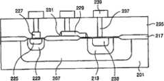
在下文中,将参照附图来详细描述本发明的实施例。实例图1是示出了根据本发明实施例的包括OTP单元的半导体器件的示意性横截面图。参照实例图1,半导体器件包括深N型阱(DeepNWell)区207和d阱(dwell)(DWell)区213,其中可以通过使用掩模对位于部分半导体衬底201上方的预定图样执行离子注入工艺来形成深N型阱区207,以及可以通过使用掩模对位于部分深N型阱区207上方的预定图样执行离子注入工艺来形成d阱区213。实例图1示出了氧化膜图样217,可以通过对形成在部分半导体衬底201上方的氧化膜执行光刻工艺(photolithography process)来形成该氧化膜图样217。实例图1还示出了浅N型阱区223和漏极区225,其中,可以通过使用掩模对位于部分深N型阱区207上方的预定图样以相对不同的剂量执行两次离子注入工艺来分别形成浅N型阱区223和漏极区225。Hereinafter, embodiments of the present invention will be described in detail with reference to the accompanying drawings. Example FIG. 1 is a schematic cross-sectional view illustrating a semiconductor device including an OTP unit according to an embodiment of the present invention. Referring to example FIG. 1, a semiconductor device includes a deep N-type well (DeepNWell)
再次参照实例图1,示出了反熔丝多晶硅图样(antifused polypattern)227和栅极多晶硅图样229,其中,可以通过对形成在部分半导体衬底201上方的栅极氧化膜执行光刻工艺来形成反熔丝多晶硅图样227和栅极多晶硅图样229。实例图1示出了侧壁隔离件231,在本发明实施例中,可以通过用预定的图样掩模刻蚀形成在栅极多晶硅图样229上方的绝缘材料,来在栅极多晶硅图样229的部分侧壁上形成侧壁隔离件231。实例图1示出了源极区233,其中,可以通过使用掩模对位于部分d阱区213上方的预定图样执行离子注入工艺来形成源极区233。此外,实例图1还示出了接触孔237,其中,可以通过在金属间介电层(inter-metal dielectric layer)235中形成接触孔区、用金属填充该接触孔区以及全面地(globally)平坦化该金属来形成接触孔237。实例图1示出了金属线239,其中,金属线239可以形成在全面平坦化的接触孔237的一部分上方,该部分可以包括接触孔237的上部。Referring again to example FIG. 1, there is shown an
实例图2A到图2H是示出了根据本发明实施例的制造半导体器件的OTP单元的步骤的示意性横截面图。参照实例图2A,可以在部分半导体衬底201上方形成氧化膜203,其中,该半导体衬底例如为硅衬底、陶瓷衬底(ceramic substrate)或聚合物衬底(polymersubstrate)。根据本发明实施例,可以在氧化膜203上方执行曝光工艺和显影工艺,以选择性地去除形成在部分半导体衬底201上方的光刻胶(PR)的一些部分,其中上述曝光工艺和显影工艺使用了刻线设计(reticle design)以具有期望的图样。结果,可以在部分氧化膜203上方形成第一PR图样205,其中该第一PR图样205可以指示出用于深N型阱的离子注入区。Example FIGS. 2A to 2H are schematic cross-sectional views illustrating steps of manufacturing an OTP unit of a semiconductor device according to an embodiment of the present invention. Referring to example FIG. 2A , an
参照实例图2B,可以使用掩模对第一PR图样205执行离子注入工艺206,以便形成深N型阱区207。在本发明实施例中,曝光工艺和显影工艺可以选择性地去除形成在部分半导体衬底201上方的PR的一些部分。结果,可以在部分氧化膜203上方形成第二PR图样209,其中,该第二PR图样209可以指示出d阱离子注入区。根据本发明实施例,可以使用掩模对第二PR图样209执行离子注入工艺211。在本发明实施例中,可以以大约1012到1014的剂量和大约40KeV到60KeV的离子注入能量来使用硼掺杂物。Referring to example FIG. 2B , an
参照实例图2C,可以在部分深N型阱区207中形成d阱区213。在本发明实施例中,可以通过对形成在部分半导体衬底201上方的氧化膜203实施光刻工艺来形成氧化膜图样217。根据本发明实施例,可以执行曝光工艺和显影工艺以选择性地去除形成在部分半导体衬底201上方的PR的一些部分。结果,可以在部分氧化膜203和氧化膜图样217上方形成第三PR图样219,其中,该第三PR图样219可以指示出用于浅N型阱区和漏极区的离子注入区。在本发明实施例中,可以使用掩模以不同的相对低的剂量对第三PR图样219执行两次离子注入工艺221。 根据本发明实施例,磷掺杂物可以被选择性地用于各个工艺。结果,可以形成浅N型阱区223和漏极区225。Referring to example FIG. 2C , d-
参照实例图2D,可以通过对形成在部分半导体衬底201上方的栅极氧化膜实施光刻工艺来形成反熔丝多晶硅图样227和栅极多晶硅图样(gate poly pattern)229。通过高电流的窄脉冲(short pulse)和高电压,可以将反熔丝多晶硅图样227的反熔丝(antifuse)分解成电阻器,从而器件可以在相对低的电压下接通,其中在通过漏极(drain)进行编程期间提供了上述高电流的窄脉冲和高电压。Referring to example FIG. 2D , an
参照实例图2E,可以通过利用预定的图样掩模来刻蚀绝缘材料,以在栅极多晶硅图样229的部分侧壁上方形成侧壁隔离件231,其中绝缘材料为诸如形成在栅极多晶硅图样229上方的氧化硅(SiO2)膜。在本发明实施例中,可以使用干法刻蚀工艺。Referring to example FIG. 2E , the insulating material may be etched by using a predetermined pattern mask to form
参照实例图2F,根据本发明实施例可以形成第四PR图样,该第四PR图样可以指示出用于源极区的离子注入区,并且可以使用掩模对第四PR图样执行离子注入工艺以便可以在d阱区213中形成源极区233。在本发明实施例中,可以使用砷掺杂物(arsenicdopant)。Referring to example FIG. 2F, a fourth PR pattern may be formed according to an embodiment of the present invention, the fourth PR pattern may indicate an ion implantation region for a source region, and an ion implantation process may be performed on the fourth PR pattern using a mask so that
参照实例图2G,可以在部分半导体衬底201上方形成金属间介电层235,并且可以在金属间介电层235中形成接触孔区域。可以在上述接触孔区域中填充金属,然后可以对所填充的接触孔区域执行化学机械抛光(CPM)工艺,从而形成全面平坦化的接触孔237。参照图2H,可以在全面平坦化的接触孔237的一部分上方形成金属线239以作为互连金属,其中,上述部分可以是全面平坦化的接触孔237的上部。Referring to example FIG. 2G , an
根据本发明实施例,使用LDMOS结构形成的OTP单元在操作期间可以承受高电压并且不受高电流的窄脉冲的影响。此外,通过在高电压编程期间消除来自ESD的任何影响来保证器件的可靠性,以及通过形成经由双扩散阱的沟道(channel)和源极来保证一致的电压,从而使器件在其电气操作中更稳定。此外,仅在通过漏极来对器件进行编程时才提供高电流的窄脉冲和高电压,这使得反熔丝被分解成电阻器,并允许用低电压来使器件导通,从而降低了器件的功耗。同样,实现了最小化的单元区域。According to an embodiment of the present invention, an OTP cell formed using an LDMOS structure can withstand a high voltage and is not affected by a narrow pulse of a high current during operation. In addition, device reliability is ensured by eliminating any influence from ESD during high-voltage programming, and by forming a channel and source through a double-diffused well to ensure consistent voltage so that the device is in its electrical operation more stable. Additionally, the narrow pulses of high current and high voltage are supplied only when programming the device through the drain, which breaks down the antifuse into a resistor and allows low voltage to turn on the device, reducing the power consumption. Also, a minimized cell area is achieved.
对于本领域技术人员显而易见和明了的是,可以对披露的本发明的实施例作各种修改和变形。因此,本发明披露的实施例意在涵盖显而易见和明了的修改和变形,只要它们在所附的权利要求及其等同替换的范围内。It will be apparent and obvious to those skilled in the art that various modifications and variations can be made to the disclosed embodiments of the invention. Thus, the disclosed embodiments of the present invention are intended to cover obvious and obvious modifications and variations provided they come within the scope of the appended claims and their equivalents.
Claims (8)
Translated fromChineseApplications Claiming Priority (2)
| Application Number | Priority Date | Filing Date | Title |
|---|---|---|---|
| KR1020080058224 | 2008-06-20 | ||
| KR1020080058224AKR100979098B1 (en) | 2008-06-20 | 2008-06-20 | Semiconductor device and method for forming OTP cell therefor |
Publications (1)
| Publication Number | Publication Date |
|---|---|
| CN101609834Atrue CN101609834A (en) | 2009-12-23 |
Family
ID=41430325
Family Applications (1)
| Application Number | Title | Priority Date | Filing Date |
|---|---|---|---|
| CNA2009101502146APendingCN101609834A (en) | 2008-06-20 | 2009-06-19 | Semiconductor device with OTP unit and manufacturing method thereof |
Country Status (4)
| Country | Link |
|---|---|
| US (1) | US20090315109A1 (en) |
| KR (1) | KR100979098B1 (en) |
| CN (1) | CN101609834A (en) |
| TW (1) | TW201001674A (en) |
Cited By (4)
| Publication number | Priority date | Publication date | Assignee | Title |
|---|---|---|---|---|
| CN103035647A (en)* | 2011-10-04 | 2013-04-10 | 美国博通公司 | One-time programmable device having an LDMOS structure and related method |
| CN103456710A (en)* | 2012-06-04 | 2013-12-18 | 中芯国际集成电路制造(上海)有限公司 | Mos device and manufacturing method thereof |
| CN106449601A (en)* | 2015-08-04 | 2017-02-22 | 无锡华润华晶微电子有限公司 | Semiconductor device manufacturing method and semiconductor device test circuit |
| CN107301877A (en)* | 2016-04-14 | 2017-10-27 | 意法半导体有限公司 | Configurable rom |
Families Citing this family (3)
| Publication number | Priority date | Publication date | Assignee | Title |
|---|---|---|---|---|
| US8164125B2 (en)* | 2010-05-07 | 2012-04-24 | Power Integrations, Inc. | Integrated transistor and anti-fuse as programming element for a high-voltage integrated circuit |
| KR102179169B1 (en) | 2014-09-02 | 2020-11-18 | 삼성전자주식회사 | Semiconductor device and method for manufacturing semiconductor device |
| US20200020707A1 (en)* | 2018-07-13 | 2020-01-16 | Ememory Technology Inc. | Semiconductor processing method for manufacturing antifuse structure with improved immunity against erroneous programming |
Citations (5)
| Publication number | Priority date | Publication date | Assignee | Title |
|---|---|---|---|---|
| US5401993A (en)* | 1990-08-30 | 1995-03-28 | Sharp Kabushiki Kaisha | Non-volatile memory |
| US6424005B1 (en)* | 1998-12-03 | 2002-07-23 | Texas Instruments Incorporated | LDMOS power device with oversized dwell |
| US20020105050A1 (en)* | 2001-02-02 | 2002-08-08 | Yoshiaki Hagiwara | One time programmable semiconductor nonvolatile memory device and method for production of same |
| US20050062125A1 (en)* | 2003-09-18 | 2005-03-24 | Makoto Kitaguchi | Lateral short-channel dmos, method of manufacturing the same, and semiconductor device |
| US20060097345A1 (en)* | 2000-08-31 | 2006-05-11 | Micron Technology, Inc. | Gate dielectric antifuse circuits and methods for operating same |
Family Cites Families (3)
| Publication number | Priority date | Publication date | Assignee | Title |
|---|---|---|---|---|
| US5909049A (en)* | 1997-02-11 | 1999-06-01 | Actel Corporation | Antifuse programmed PROM cell |
| JP4484984B2 (en) | 1999-07-30 | 2010-06-16 | 富士通マイクロエレクトロニクス株式会社 | Manufacturing method of semiconductor memory device |
| JP2001351993A (en) | 2000-06-05 | 2001-12-21 | Nec Corp | Semiconductor memory device and method of manufacturing the same |
- 2008
- 2008-06-20KRKR1020080058224Apatent/KR100979098B1/ennot_activeExpired - Fee Related
- 2009
- 2009-06-15USUS12/484,305patent/US20090315109A1/ennot_activeAbandoned
- 2009-06-19CNCNA2009101502146Apatent/CN101609834A/enactivePending
- 2009-06-19TWTW098120753Apatent/TW201001674A/enunknown
Patent Citations (5)
| Publication number | Priority date | Publication date | Assignee | Title |
|---|---|---|---|---|
| US5401993A (en)* | 1990-08-30 | 1995-03-28 | Sharp Kabushiki Kaisha | Non-volatile memory |
| US6424005B1 (en)* | 1998-12-03 | 2002-07-23 | Texas Instruments Incorporated | LDMOS power device with oversized dwell |
| US20060097345A1 (en)* | 2000-08-31 | 2006-05-11 | Micron Technology, Inc. | Gate dielectric antifuse circuits and methods for operating same |
| US20020105050A1 (en)* | 2001-02-02 | 2002-08-08 | Yoshiaki Hagiwara | One time programmable semiconductor nonvolatile memory device and method for production of same |
| US20050062125A1 (en)* | 2003-09-18 | 2005-03-24 | Makoto Kitaguchi | Lateral short-channel dmos, method of manufacturing the same, and semiconductor device |
Cited By (9)
| Publication number | Priority date | Publication date | Assignee | Title |
|---|---|---|---|---|
| CN103035647A (en)* | 2011-10-04 | 2013-04-10 | 美国博通公司 | One-time programmable device having an LDMOS structure and related method |
| US8932912B2 (en) | 2011-10-04 | 2015-01-13 | Broadcom Corporation | One-time programmable device |
| US8969957B2 (en) | 2011-10-04 | 2015-03-03 | Broadcom Corporation | LDMOS one-time programmable device |
| CN103035647B (en)* | 2011-10-04 | 2016-12-07 | 美国博通公司 | There is disposal programmable device and the correlation technique of LDMOS structure |
| CN103456710A (en)* | 2012-06-04 | 2013-12-18 | 中芯国际集成电路制造(上海)有限公司 | Mos device and manufacturing method thereof |
| CN103456710B (en)* | 2012-06-04 | 2016-06-01 | 中芯国际集成电路制造(上海)有限公司 | MOS device and manufacture method thereof |
| CN106449601A (en)* | 2015-08-04 | 2017-02-22 | 无锡华润华晶微电子有限公司 | Semiconductor device manufacturing method and semiconductor device test circuit |
| CN106449601B (en)* | 2015-08-04 | 2019-04-16 | 无锡华润华晶微电子有限公司 | A kind of manufacturing method of semiconductor devices and test circuit |
| CN107301877A (en)* | 2016-04-14 | 2017-10-27 | 意法半导体有限公司 | Configurable rom |
Also Published As
| Publication number | Publication date |
|---|---|
| KR100979098B1 (en) | 2010-08-31 |
| KR20090132121A (en) | 2009-12-30 |
| US20090315109A1 (en) | 2009-12-24 |
| TW201001674A (en) | 2010-01-01 |
Similar Documents
| Publication | Publication Date | Title |
|---|---|---|
| US8716831B2 (en) | One time programmable structure using a gate last high-K metal gate process | |
| CN101609834A (en) | Semiconductor device with OTP unit and manufacturing method thereof | |
| CN112635468B (en) | An antifuse one-time programmable memory cell | |
| US9153684B2 (en) | Semiconductor fuses in a semiconductor device comprising metal gates | |
| CN105849861A (en) | Anti-fuse memory cell | |
| CN114078757A (en) | Method for manufacturing semiconductor element | |
| CN112234063B (en) | One-time programmable memory cell of antifuse | |
| CN102054817B (en) | Antifuse and method for manufacturing antifuse | |
| KR101531883B1 (en) | A horizontal-type dimos transistor | |
| CN103794549B (en) | Formation method of semiconductor structure | |
| CN113611703B (en) | Method for manufacturing semiconductor structure | |
| KR100535854B1 (en) | Semiconductor device and manufacturing method thereof | |
| US12178039B2 (en) | Memory device having merged active area | |
| KR20090057744A (en) | Semiconductor element and manufacturing method thereof | |
| CN112234062A (en) | Anti-fuse one-time programmable memory unit | |
| TWI855817B (en) | Semiconductor device structure including fuse structure embedded in substrate | |
| US20080035981A1 (en) | One time programmable memory and the manufacturing method thereof | |
| US20230180469A1 (en) | Method for manufacturing memory device having merged active area | |
| KR101015524B1 (en) | Semiconductor device and manufacturing method thereof | |
| KR100567025B1 (en) | Mask ROM Cell Manufacturing Method | |
| JP2005322730A (en) | Semiconductor device and manufacturing method therefor | |
| TWI553865B (en) | Power MOS semi-transistor element | |
| CN101499423B (en) | Semiconductor element, manufacturing method thereof, and complementary semiconductor element manufacturing method | |
| HK1179760B (en) | A semiconductor device having an efuse structure for a one time programmable memory | |
| KR20060073131A (en) | Semiconductor device manufacturing method |
Legal Events
| Date | Code | Title | Description |
|---|---|---|---|
| C06 | Publication | ||
| PB01 | Publication | ||
| C10 | Entry into substantive examination | ||
| SE01 | Entry into force of request for substantive examination | ||
| C02 | Deemed withdrawal of patent application after publication (patent law 2001) | ||
| WD01 | Invention patent application deemed withdrawn after publication | Application publication date:20091223 |