CN101609822A - Package structure for chip reconfiguration and method thereof - Google Patents
Package structure for chip reconfiguration and method thereofDownload PDFInfo
- Publication number
- CN101609822A CN101609822ACNA2008101102740ACN200810110274ACN101609822ACN 101609822 ACN101609822 ACN 101609822ACN A2008101102740 ACNA2008101102740 ACN A2008101102740ACN 200810110274 ACN200810110274 ACN 200810110274ACN 101609822 ACN101609822 ACN 101609822A
- Authority
- CN
- China
- Prior art keywords
- polymer material
- material layer
- chip
- forming
- metal line
- Prior art date
- Legal status (The legal status is an assumption and is not a legal conclusion. Google has not performed a legal analysis and makes no representation as to the accuracy of the status listed.)
- Pending
Links
- 238000000034methodMethods0.000titleclaimsabstractdescription53
- 239000002861polymer materialSubstances0.000claimsabstractdescription108
- 239000002184metalSubstances0.000claimsabstractdescription88
- 229910052751metalInorganic materials0.000claimsabstractdescription88
- 238000004806packaging method and processMethods0.000claimsabstractdescription34
- 238000007789sealingMethods0.000claimsabstractdescription10
- 229910000679solderInorganic materials0.000claimsabstractdescription6
- 239000010410layerSubstances0.000claimsdescription116
- 239000000758substrateSubstances0.000claimsdescription45
- 235000012431wafersNutrition0.000claimsdescription39
- 239000008393encapsulating agentSubstances0.000claimsdescription32
- 239000012790adhesive layerSubstances0.000claimsdescription26
- 238000003466weldingMethods0.000claimsdescription17
- 239000010949copperSubstances0.000claimsdescription14
- 230000006870functionEffects0.000claimsdescription13
- 239000011241protective layerSubstances0.000claimsdescription11
- RYGMFSIKBFXOCR-UHFFFAOYSA-NCopperChemical compound[Cu]RYGMFSIKBFXOCR-UHFFFAOYSA-N0.000claimsdescription10
- 229910052802copperInorganic materials0.000claimsdescription10
- 239000000565sealantSubstances0.000claimsdescription7
- 229910000881Cu alloyInorganic materials0.000claimsdescription4
- 239000000084colloidal systemSubstances0.000claimsdescription4
- 238000005520cutting processMethods0.000description15
- 239000004065semiconductorSubstances0.000description12
- 239000000463materialSubstances0.000description8
- 238000005516engineering processMethods0.000description5
- 238000004519manufacturing processMethods0.000description5
- 238000010586diagramMethods0.000description4
- 238000012858packaging processMethods0.000description4
- 238000012536packaging technologyMethods0.000description4
- 239000004642PolyimideSubstances0.000description3
- 229920002120photoresistant polymerPolymers0.000description3
- 229920001721polyimidePolymers0.000description3
- 238000003860storageMethods0.000description3
- 229910001020Au alloyInorganic materials0.000description2
- 229920000800acrylic rubberPolymers0.000description2
- UMIVXZPTRXBADB-UHFFFAOYSA-NbenzocyclobuteneChemical compoundC1=CC=C2CCC2=C1UMIVXZPTRXBADB-UHFFFAOYSA-N0.000description2
- 238000005229chemical vapour depositionMethods0.000description2
- 230000008878couplingEffects0.000description2
- 238000010168coupling processMethods0.000description2
- 238000005859coupling reactionMethods0.000description2
- 238000005530etchingMethods0.000description2
- PCHJSUWPFVWCPO-UHFFFAOYSA-NgoldChemical compound[Au]PCHJSUWPFVWCPO-UHFFFAOYSA-N0.000description2
- 239000010931goldSubstances0.000description2
- 238000001746injection mouldingMethods0.000description2
- 238000005240physical vapour depositionMethods0.000description2
- 229920000058polyacrylatePolymers0.000description2
- VYPSYNLAJGMNEJ-UHFFFAOYSA-Nsilicon dioxideInorganic materialsO=[Si]=OVYPSYNLAJGMNEJ-UHFFFAOYSA-N0.000description2
- 229920002379silicone rubberPolymers0.000description2
- 238000005476solderingMethods0.000description2
- 238000012360testing methodMethods0.000description2
- XUIMIQQOPSSXEZ-UHFFFAOYSA-NSiliconChemical compound[Si]XUIMIQQOPSSXEZ-UHFFFAOYSA-N0.000description1
- ATJFFYVFTNAWJD-UHFFFAOYSA-NTinChemical compound[Sn]ATJFFYVFTNAWJD-UHFFFAOYSA-N0.000description1
- NIXOWILDQLNWCW-UHFFFAOYSA-Nacrylic acid groupChemical groupC(C=C)(=O)ONIXOWILDQLNWCW-UHFFFAOYSA-N0.000description1
- 239000000853adhesiveSubstances0.000description1
- 230000001070adhesive effectEffects0.000description1
- 229910045601alloyInorganic materials0.000description1
- 239000000956alloySubstances0.000description1
- 230000015572biosynthetic processEffects0.000description1
- 239000000919ceramicSubstances0.000description1
- 239000011248coating agentSubstances0.000description1
- 238000000576coating methodMethods0.000description1
- 239000003086colorantSubstances0.000description1
- 238000002425crystallisationMethods0.000description1
- 230000008025crystallizationEffects0.000description1
- 210000005069earsAnatomy0.000description1
- 238000009713electroplatingMethods0.000description1
- 239000003822epoxy resinSubstances0.000description1
- 239000011888foilSubstances0.000description1
- 239000011521glassSubstances0.000description1
- 239000003292glueSubstances0.000description1
- 238000000227grindingMethods0.000description1
- 239000007769metal materialSubstances0.000description1
- 239000005022packaging materialSubstances0.000description1
- 229920000647polyepoxidePolymers0.000description1
- 239000010453quartzSubstances0.000description1
- 229920005989resinPolymers0.000description1
- 239000011347resinSubstances0.000description1
- 239000000741silica gelSubstances0.000description1
- 229910002027silica gelInorganic materials0.000description1
- 229910052710siliconInorganic materials0.000description1
- 239000010703siliconSubstances0.000description1
- 229920002050silicone resinPolymers0.000description1
- 239000000243solutionSubstances0.000description1
- 230000009897systematic effectEffects0.000description1
Images


Classifications
- H—ELECTRICITY
- H01—ELECTRIC ELEMENTS
- H01L—SEMICONDUCTOR DEVICES NOT COVERED BY CLASS H10
- H01L24/00—Arrangements for connecting or disconnecting semiconductor or solid-state bodies; Methods or apparatus related thereto
- H01L24/93—Batch processes
- H01L24/95—Batch processes at chip-level, i.e. with connecting carried out on a plurality of singulated devices, i.e. on diced chips
- H01L24/96—Batch processes at chip-level, i.e. with connecting carried out on a plurality of singulated devices, i.e. on diced chips the devices being encapsulated in a common layer, e.g. neo-wafer or pseudo-wafer, said common layer being separable into individual assemblies after connecting
- H—ELECTRICITY
- H01—ELECTRIC ELEMENTS
- H01L—SEMICONDUCTOR DEVICES NOT COVERED BY CLASS H10
- H01L21/00—Processes or apparatus adapted for the manufacture or treatment of semiconductor or solid state devices or of parts thereof
- H01L21/67—Apparatus specially adapted for handling semiconductor or electric solid state devices during manufacture or treatment thereof; Apparatus specially adapted for handling wafers during manufacture or treatment of semiconductor or electric solid state devices or components ; Apparatus not specifically provided for elsewhere
- H01L21/683—Apparatus specially adapted for handling semiconductor or electric solid state devices during manufacture or treatment thereof; Apparatus specially adapted for handling wafers during manufacture or treatment of semiconductor or electric solid state devices or components ; Apparatus not specifically provided for elsewhere for supporting or gripping
- H01L21/6835—Apparatus specially adapted for handling semiconductor or electric solid state devices during manufacture or treatment thereof; Apparatus specially adapted for handling wafers during manufacture or treatment of semiconductor or electric solid state devices or components ; Apparatus not specifically provided for elsewhere for supporting or gripping using temporarily an auxiliary support
- H—ELECTRICITY
- H01—ELECTRIC ELEMENTS
- H01L—SEMICONDUCTOR DEVICES NOT COVERED BY CLASS H10
- H01L21/00—Processes or apparatus adapted for the manufacture or treatment of semiconductor or solid state devices or of parts thereof
- H01L21/02—Manufacture or treatment of semiconductor devices or of parts thereof
- H01L21/04—Manufacture or treatment of semiconductor devices or of parts thereof the devices having potential barriers, e.g. a PN junction, depletion layer or carrier concentration layer
- H01L21/50—Assembly of semiconductor devices using processes or apparatus not provided for in a single one of the groups H01L21/18 - H01L21/326 or H10D48/04 - H10D48/07 e.g. sealing of a cap to a base of a container
- H01L21/56—Encapsulations, e.g. encapsulation layers, coatings
- H01L21/568—Temporary substrate used as encapsulation process aid
- H—ELECTRICITY
- H01—ELECTRIC ELEMENTS
- H01L—SEMICONDUCTOR DEVICES NOT COVERED BY CLASS H10
- H01L2224/00—Indexing scheme for arrangements for connecting or disconnecting semiconductor or solid-state bodies and methods related thereto as covered by H01L24/00
- H01L2224/01—Means for bonding being attached to, or being formed on, the surface to be connected, e.g. chip-to-package, die-attach, "first-level" interconnects; Manufacturing methods related thereto
- H01L2224/02—Bonding areas; Manufacturing methods related thereto
- H01L2224/04—Structure, shape, material or disposition of the bonding areas prior to the connecting process
- H01L2224/04105—Bonding areas formed on an encapsulation of the semiconductor or solid-state body, e.g. bonding areas on chip-scale packages
- H—ELECTRICITY
- H01—ELECTRIC ELEMENTS
- H01L—SEMICONDUCTOR DEVICES NOT COVERED BY CLASS H10
- H01L2224/00—Indexing scheme for arrangements for connecting or disconnecting semiconductor or solid-state bodies and methods related thereto as covered by H01L24/00
- H01L2224/01—Means for bonding being attached to, or being formed on, the surface to be connected, e.g. chip-to-package, die-attach, "first-level" interconnects; Manufacturing methods related thereto
- H01L2224/10—Bump connectors; Manufacturing methods related thereto
- H01L2224/12—Structure, shape, material or disposition of the bump connectors prior to the connecting process
- H01L2224/12105—Bump connectors formed on an encapsulation of the semiconductor or solid-state body, e.g. bumps on chip-scale packages
- H—ELECTRICITY
- H01—ELECTRIC ELEMENTS
- H01L—SEMICONDUCTOR DEVICES NOT COVERED BY CLASS H10
- H01L2224/00—Indexing scheme for arrangements for connecting or disconnecting semiconductor or solid-state bodies and methods related thereto as covered by H01L24/00
- H01L2224/01—Means for bonding being attached to, or being formed on, the surface to be connected, e.g. chip-to-package, die-attach, "first-level" interconnects; Manufacturing methods related thereto
- H01L2224/18—High density interconnect [HDI] connectors; Manufacturing methods related thereto
- H01L2224/19—Manufacturing methods of high density interconnect preforms
- H—ELECTRICITY
- H01—ELECTRIC ELEMENTS
- H01L—SEMICONDUCTOR DEVICES NOT COVERED BY CLASS H10
- H01L2224/00—Indexing scheme for arrangements for connecting or disconnecting semiconductor or solid-state bodies and methods related thereto as covered by H01L24/00
- H01L2224/01—Means for bonding being attached to, or being formed on, the surface to be connected, e.g. chip-to-package, die-attach, "first-level" interconnects; Manufacturing methods related thereto
- H01L2224/18—High density interconnect [HDI] connectors; Manufacturing methods related thereto
- H01L2224/20—Structure, shape, material or disposition of high density interconnect preforms
- H—ELECTRICITY
- H01—ELECTRIC ELEMENTS
- H01L—SEMICONDUCTOR DEVICES NOT COVERED BY CLASS H10
- H01L2224/00—Indexing scheme for arrangements for connecting or disconnecting semiconductor or solid-state bodies and methods related thereto as covered by H01L24/00
- H01L2224/01—Means for bonding being attached to, or being formed on, the surface to be connected, e.g. chip-to-package, die-attach, "first-level" interconnects; Manufacturing methods related thereto
- H01L2224/18—High density interconnect [HDI] connectors; Manufacturing methods related thereto
- H01L2224/23—Structure, shape, material or disposition of the high density interconnect connectors after the connecting process
- H01L2224/24—Structure, shape, material or disposition of the high density interconnect connectors after the connecting process of an individual high density interconnect connector
- H01L2224/241—Disposition
- H01L2224/24135—Connecting between different semiconductor or solid-state bodies, i.e. chip-to-chip
- H01L2224/24137—Connecting between different semiconductor or solid-state bodies, i.e. chip-to-chip the bodies being arranged next to each other, e.g. on a common substrate
- H—ELECTRICITY
- H01—ELECTRIC ELEMENTS
- H01L—SEMICONDUCTOR DEVICES NOT COVERED BY CLASS H10
- H01L2924/00—Indexing scheme for arrangements or methods for connecting or disconnecting semiconductor or solid-state bodies as covered by H01L24/00
- H01L2924/01—Chemical elements
- H01L2924/01015—Phosphorus [P]
- H—ELECTRICITY
- H01—ELECTRIC ELEMENTS
- H01L—SEMICONDUCTOR DEVICES NOT COVERED BY CLASS H10
- H01L2924/00—Indexing scheme for arrangements or methods for connecting or disconnecting semiconductor or solid-state bodies as covered by H01L24/00
- H01L2924/01—Chemical elements
- H01L2924/01023—Vanadium [V]
- H—ELECTRICITY
- H01—ELECTRIC ELEMENTS
- H01L—SEMICONDUCTOR DEVICES NOT COVERED BY CLASS H10
- H01L2924/00—Indexing scheme for arrangements or methods for connecting or disconnecting semiconductor or solid-state bodies as covered by H01L24/00
- H01L2924/01—Chemical elements
- H01L2924/01029—Copper [Cu]
- H—ELECTRICITY
- H01—ELECTRIC ELEMENTS
- H01L—SEMICONDUCTOR DEVICES NOT COVERED BY CLASS H10
- H01L2924/00—Indexing scheme for arrangements or methods for connecting or disconnecting semiconductor or solid-state bodies as covered by H01L24/00
- H01L2924/01—Chemical elements
- H01L2924/01033—Arsenic [As]
- H—ELECTRICITY
- H01—ELECTRIC ELEMENTS
- H01L—SEMICONDUCTOR DEVICES NOT COVERED BY CLASS H10
- H01L2924/00—Indexing scheme for arrangements or methods for connecting or disconnecting semiconductor or solid-state bodies as covered by H01L24/00
- H01L2924/01—Chemical elements
- H01L2924/01068—Erbium [Er]
- H—ELECTRICITY
- H01—ELECTRIC ELEMENTS
- H01L—SEMICONDUCTOR DEVICES NOT COVERED BY CLASS H10
- H01L2924/00—Indexing scheme for arrangements or methods for connecting or disconnecting semiconductor or solid-state bodies as covered by H01L24/00
- H01L2924/01—Chemical elements
- H01L2924/01078—Platinum [Pt]
- H—ELECTRICITY
- H01—ELECTRIC ELEMENTS
- H01L—SEMICONDUCTOR DEVICES NOT COVERED BY CLASS H10
- H01L2924/00—Indexing scheme for arrangements or methods for connecting or disconnecting semiconductor or solid-state bodies as covered by H01L24/00
- H01L2924/01—Chemical elements
- H01L2924/01079—Gold [Au]
- H—ELECTRICITY
- H01—ELECTRIC ELEMENTS
- H01L—SEMICONDUCTOR DEVICES NOT COVERED BY CLASS H10
- H01L2924/00—Indexing scheme for arrangements or methods for connecting or disconnecting semiconductor or solid-state bodies as covered by H01L24/00
- H01L2924/01—Chemical elements
- H01L2924/01094—Plutonium [Pu]
- H—ELECTRICITY
- H01—ELECTRIC ELEMENTS
- H01L—SEMICONDUCTOR DEVICES NOT COVERED BY CLASS H10
- H01L2924/00—Indexing scheme for arrangements or methods for connecting or disconnecting semiconductor or solid-state bodies as covered by H01L24/00
- H01L2924/15—Details of package parts other than the semiconductor or other solid state devices to be connected
- H01L2924/151—Die mounting substrate
- H01L2924/153—Connection portion
- H01L2924/1531—Connection portion the connection portion being formed only on the surface of the substrate opposite to the die mounting surface
- H01L2924/15311—Connection portion the connection portion being formed only on the surface of the substrate opposite to the die mounting surface being a ball array, e.g. BGA
- H—ELECTRICITY
- H01—ELECTRIC ELEMENTS
- H01L—SEMICONDUCTOR DEVICES NOT COVERED BY CLASS H10
- H01L2924/00—Indexing scheme for arrangements or methods for connecting or disconnecting semiconductor or solid-state bodies as covered by H01L24/00
- H01L2924/30—Technical effects
- H01L2924/35—Mechanical effects
- H01L2924/351—Thermal stress
- H01L2924/3511—Warping
Landscapes
- Engineering & Computer Science (AREA)
- Computer Hardware Design (AREA)
- Microelectronics & Electronic Packaging (AREA)
- Power Engineering (AREA)
- Physics & Mathematics (AREA)
- Condensed Matter Physics & Semiconductors (AREA)
- General Physics & Mathematics (AREA)
- Manufacturing & Machinery (AREA)
- Dicing (AREA)
Abstract
Translated fromChinese
Description
Translated fromChinese技术领域technical field
本发明有关一种半导体封装方法,特别是将不同尺寸大小及功能的芯片进行重新配置的封装方法。The invention relates to a semiconductor packaging method, in particular to a packaging method for reconfiguring chips with different sizes and functions.
背景技术Background technique
半导体的技术已经发展的相当的迅速,因此微型化的半导体芯片(Dice)必须具有多样化的功能的需求,使得半导体芯片必须要在很小的区域中配置更多的输入/输出垫(I/O pads),因而使得金属接脚(pins)的密度也快速的提高了。因此,早期的导线架封装技术已经不适合高密度的金属接脚;故发展出一种球阵列(BallGrid Array:BGA)的封装技术,球阵列封装除了有比导线架封装更高密度的优点外,其锡球也比较不容易损害与变形。Semiconductor technology has developed quite rapidly, so the miniaturized semiconductor chip (Dice) must have diversified functional requirements, so that the semiconductor chip must be configured with more input/output pads (I/O pads) in a small area. O pads), so that the density of metal pins (pins) is also rapidly increased. Therefore, the early lead frame packaging technology is no longer suitable for high-density metal pins; therefore, a ball array (BallGrid Array: BGA) packaging technology has been developed. In addition to the advantages of higher density than lead frame packaging, ball array packaging , and its tin balls are less likely to be damaged and deformed.
随着3C产品的流行,例如:移动电话(Cell Phone)、个人数字助理(PDA)或是iPod等,都必须要将许多复杂的系统芯片放入一个非常小的空间中,因此为解决此一问题,一种称为“晶片级封装(wafer level package;WLP)”的封装技术已经发展出来,其可以在切割晶片成为一个个的芯片之前,就先对晶片进行封装。美国专利公告第5,323,051号专利即揭露了这种“晶片级封装”技术。然而,这种“晶片级封装”技术随着芯片主动面上的焊垫(pads)数目的增加,使得焊垫(pads)的间距过小,除了会导致信号耦合或信号干扰的问题外,也会因为焊垫间距过小而造成封装的可靠度降低等问题。因此,当芯片再更进一步的缩小后,使得前述的封装技术都无法满足。With the popularity of 3C products, such as: mobile phone (Cell Phone), personal digital assistant (PDA) or iPod, etc., it is necessary to put many complex system chips into a very small space, so in order to solve this problem The problem is that a packaging technology called "wafer level package (WLP)" has been developed, which can package the wafer before cutting the wafer into individual chips. US Patent Publication No. 5,323,051 discloses this "wafer level packaging" technology. However, this "wafer level packaging" technology increases the number of pads (pads) on the active surface of the chip, making the pitch of the pads (pads) too small, which will not only cause problems of signal coupling or signal interference, but also Problems such as reduced reliability of the package will be caused due to the too small pitch of the pads. Therefore, when the chip is further shrunk, the above-mentioned packaging technology cannot be satisfied.
为解决此一问题,美国专利公告第7,196,408号已揭露了一种将完成半导体制程的晶片,经过测试及切割后,将测试结果为良好的芯片(good die)重新放置于另一个基板之上,然后再进行封装工序,如此,使得这些被重新放置的芯片间具有较宽的间距,故可以将芯片上的焊垫适当的分配,例如使用向外延伸(fan out)技术,因此可以有效解决因间距过小,除了会导致信号耦合或信号干扰的问题。In order to solve this problem, U.S. Patent No. 7,196,408 has disclosed a wafer that will complete the semiconductor manufacturing process. After testing and cutting, the test result is a good chip (good die) that is replaced on another substrate. Then the packaging process is carried out, so that these relocated chips have a wider spacing, so the pads on the chips can be properly allocated, such as using the outward extension (fan out) technology, so it can effectively solve the problem. If the spacing is too small, it will cause problems with signal coupling or signal interference.
然而,为使半导体芯片能够有较小及较薄的封装结构,在进行晶片切割前,会先对晶片进行薄化处理,例如以背磨(backside lapping)方式将晶片薄化至2~20密耳(mil),然后再切割成一个个的芯片。此一经过薄化处理的芯片,经过重新配置在另一基板上,再以注模方式将多个芯片形成一封胶体;由于芯片很薄,使得封胶体也是非常的薄,故当封胶体脱离基板之后,封胶体本身的应力会使得封胶体产生翘曲,增加后续进行切割工序的困难。However, in order to enable the semiconductor chip to have a smaller and thinner packaging structure, before the wafer is cut, the wafer will be thinned, for example, the wafer is thinned to 2-20 densities by backside lapping. ears (mil), and then cut into individual chips. This thinned chip is relocated on another substrate, and then multiple chips are formed into a package by injection molding; because the chip is very thin, the package is also very thin, so when the package is detached After the substrate, the stress of the encapsulant itself will cause the encapsulant to warp, increasing the difficulty of the subsequent cutting process.
另外,在晶片切割之后,重新配置在另一个基板时,由于新的基板的尺寸较原来的尺寸为大,因此在后续植球工序中,会无法对准,其封装结构可靠度降低。为此,本发明提供一种预先将铜柱形成于芯片上的焊垫,然后再通过薄化工序将铜柱曝露出来,故可以有效地解决植球时无法对准以及封胶体产生翘曲的问题。In addition, after the wafer is diced, when it is reconfigured on another substrate, since the size of the new substrate is larger than the original size, alignment will not be possible in the subsequent ball-planting process, and the reliability of the packaging structure will be reduced. For this reason, the present invention provides a soldering pad on which the copper column is formed in advance on the chip, and then the copper column is exposed through the thinning process, so that it can effectively solve the problems of misalignment during ball planting and warping of the encapsulant question.
此外,在整个封装的过程中,还会产生植球时,制造设备会对芯片产生局部过大的压力,而可能损伤芯片的问题;同时,也可能因为植球的材料造成与芯片上的焊垫间的电阻值变大,而影响芯片的性能等问题。为此,本发明提供再一种预先将铜柱形成于芯片上的焊垫,然后再通过薄化工序将铜柱暴露出来,接着再以向外延伸(fan out)技术将植球做适当的配置,除可有效解决损伤芯片的问题,也可同时解决焊垫的间距过小等问题。In addition, during the entire packaging process, there will also be a problem that the manufacturing equipment will generate excessive local pressure on the chip during ball planting, which may damage the chip; at the same time, it may also be caused by the material of the ball planting. The resistance value between the pads becomes larger, which affects problems such as chip performance. For this reason, the present invention provides yet another kind of soldering pad that copper column is formed on the chip in advance, then copper column is exposed through thinning process, and then outward extension (fan out) technique is done proper ball planting Configuration, in addition to effectively solving the problem of chip damage, it can also solve the problem of too small spacing of the pads at the same time.
发明内容Contents of the invention
有鉴于发明背景中所述的植球对准以及封胶体翘曲的问题,本发明提供一种利用芯片重新配置的封装结构及其方法,来将多个芯片重新进行配置并进行封装的方法。故本发明的主要目的在于提供一种在芯片上形成导电柱,然后通过薄化工序将导电柱曝露出来,以便在芯片重新配置的封装过程中可以对准,可有效提高制造的良率及可靠度。In view of the problems of ball-planting alignment and encapsulant warpage described in the background of the invention, the present invention provides a method for reconfiguring and packaging a plurality of chips using a chip reconfiguration packaging structure and method thereof. Therefore, the main purpose of the present invention is to provide a method of forming conductive pillars on a chip, and then exposing the conductive pillars through a thinning process, so that they can be aligned during the chip reconfiguration packaging process, which can effectively improve the manufacturing yield and reliability. Spend.
本发明的另一主要目的在于提供一种在芯片重新配置的封装结构及其方法,是将不同尺寸大小及功能的芯片重新配置在一基板上的封装方法。Another main purpose of the present invention is to provide a packaging structure and method for reconfiguring chips, which is a packaging method for reconfiguring chips with different sizes and functions on a substrate.
本发明的再一主要目的在于提供一种在芯片重新配置的封装结构及其方法,是在封胶体的表面上形成多条沟渠,可防止封胶体在脱离基板后,产生翘曲的现象,而提高制造良率。Another main purpose of the present invention is to provide a packaging structure and method for chip reconfiguration, in which a plurality of trenches are formed on the surface of the encapsulant to prevent the encapsulant from warping after it is detached from the substrate. Improve manufacturing yield.
此外,本发明还有一主要目的在于提供一种芯片重新配置的封装方法,其可以将12时晶片所切割出来的芯片重新配置于8时晶片的基板上,如此可以有效运用8时晶片的即有的封装设备,而无需重新设立12时晶片的封装设备,可以降低12时晶片的封装成本。In addition, another main purpose of the present invention is to provide a packaging method for chip reconfiguration, which can reconfigure the chips cut from the 12 o'clock wafer on the substrate of the 8 o'clock wafer, so that the existing chips of the 8 o'clock wafer can be effectively used. The package equipment of 12 o'clock chip can reduce the package cost of 12 o'clock chip without re-establishing the package equipment of 12 o'clock chip.
本发明的再一主要目的在于提供一种芯片重新配置的封装方法,使得进行封装的芯片都是“已知是功能正常的芯片”(Known good die),可以节省封装材料,故也可以降低工序的成本Another main purpose of the present invention is to provide a packaging method for chip reconfiguration, so that the packaged chips are all "known good dies", which can save packaging materials, so it can also reduce the process. the cost of
根据以上所述,本发明提供一种芯片重新配置的封装结构,包括:于主动面上配置有多个焊垫的芯片;一第一高分子材料层,覆盖于芯片的主动面上并曝露出多个焊垫;多个导电柱,其配置于第一高分子材料层之间并与多个曝露的焊垫电性连接;一封胶体,用以包覆芯片的五个面且曝露出第一高分子材料层及多个导电柱;一第二高分子材料层,覆盖于第一高分子材料层及封胶体上并曝露出多个导电柱;多条扇出的金属线段,其配置于第二高分子材料层之上且每一金属线段的一端与导电柱电性连接;一保护层,其覆盖第二高分子材料层及金属线段上并曝露出金属线段的另一端的一上表面;多个导电元件,其与金属线段的另一端电性连接。According to the above, the present invention provides a package structure for chip reconfiguration, including: a chip with a plurality of pads disposed on the active surface; a first polymer material layer covering the active surface of the chip and exposing A plurality of welding pads; a plurality of conductive pillars, which are arranged between the first polymer material layer and electrically connected with a plurality of exposed welding pads; A polymer material layer and a plurality of conductive pillars; a second polymer material layer covering the first polymer material layer and the sealant and exposing a plurality of conductive pillars; a plurality of fan-out metal line segments, which are arranged on On the second polymer material layer and one end of each metal line segment is electrically connected to the conductive column; a protective layer covers the second polymer material layer and the metal line segment and exposes an upper surface of the other end of the metal line segment ; A plurality of conductive elements, which are electrically connected to the other end of the metal wire segment.
本发明接着提供一种模块化的多芯片封装结构,包括:多个芯片,每一芯片的主动面上配置有多个焊垫;一第一高分子材料层,覆盖于每一芯片的主动面上并曝露多个焊垫;多个导电柱,其配置于第一高分子材料层之间并与多个曝露的焊垫电性连接;一封装体,其环覆于每一芯片的五个面且曝露出第一高分子材料层及多个导电柱;一第二高分子材料层,覆盖于第一高分子材料层及封胶体上并曝露出多个导电柱;多个图案化的金属线段,其配置于第二高分子材料层之上,且部份图案化的金属线段的两端电性连接这些导电柱,而部份图案化的金属线段的一端电性连接这些导电柱;一图案化的保护层,其覆盖第二高分子材料层及图案化的金属线段上并曝露部份图案化的金属线段的另一端;多个导电元件,其与金属线段的另一端电性连接。The present invention then provides a modular multi-chip packaging structure, including: a plurality of chips, each of which is equipped with a plurality of pads on the active surface; a first polymer material layer covering the active surface of each chip and expose a plurality of welding pads; a plurality of conductive columns, which are arranged between the first polymer material layer and electrically connected with a plurality of exposed welding pads; a package, which surrounds five of each chip surface and expose the first polymer material layer and a plurality of conductive pillars; a second polymer material layer covers the first polymer material layer and the sealing body and exposes a plurality of conductive pillars; a plurality of patterned metal a line segment, which is disposed on the second polymer material layer, and the two ends of the partially patterned metal line segment are electrically connected to the conductive pillars, and one end of the partially patterned metal line segment is electrically connected to the conductive pillars; A patterned protection layer covers the second polymer material layer and the patterned metal line segment and exposes part of the other end of the patterned metal line segment; a plurality of conductive elements are electrically connected to the other end of the metal line segment.
本发明接着提供多芯片封装方法,包括:提供一晶片,其主动面上形成有多个芯片区且每一芯片区的主动上配置有多个焊垫;形成一第一高分子材料层于晶片上,以覆盖每一芯片区及每一焊垫;形成多个第一开口,是于第一高分子材料层上形成多个开口,以曝露出每一焊垫;形成多个导电柱于每一第一开口中,并使多个导电柱的一端与每一焊垫电性连接;切割该晶片,以形成多个独立的芯片;提供一基板,并于基板上配置一黏着层;以覆晶方式将每一芯片取放至黏着层上;形成一封胶体,是将一第二高分子材料层环覆于每一芯片之间并于黏着层上形成一封胶体;分离基板及封胶体,以曝露出第一高分子材料层、第二高分子材料层及多个导电柱;形成一第三高分子材料层于第一高分子材料层及第二高分子材料层上;于第三高分子材料层上形成多个第二开口并曝露出每一导电柱;形成多个图案化的金属线段于第三高分子材料层上,每一图案化的金属线段的一端电性连接于每一导电柱;形成一图案化的保护层以覆盖这些图案化的金属线段,并曝露出图案化的金属线段的另一端;形成多个导电元件于图案化的金属线段的另一端上;及切割封胶体,以形成多个芯片封装结构或是多个多芯片的封装结构。The present invention then provides a multi-chip packaging method, comprising: providing a wafer with a plurality of chip regions formed on its active surface and a plurality of pads disposed on the active surface of each chip region; forming a first polymer material layer on the wafer to cover each chip area and each welding pad; forming a plurality of first openings is to form a plurality of openings on the first polymer material layer to expose each welding pad; forming a plurality of conductive columns on each a first opening, and electrically connect one end of a plurality of conductive pillars to each pad; cut the wafer to form a plurality of independent chips; provide a substrate, and configure an adhesive layer on the substrate; to cover Take and place each chip on the adhesive layer by means of crystallization; form a sealant, which is to wrap a second polymer material layer between each chip and form a sealant on the adhesive layer; separate the substrate and the sealant , to expose the first polymer material layer, the second polymer material layer and a plurality of conductive pillars; form a third polymer material layer on the first polymer material layer and the second polymer material layer; in the third A plurality of second openings are formed on the polymer material layer to expose each conductive column; a plurality of patterned metal line segments are formed on the third polymer material layer, and one end of each patterned metal line segment is electrically connected to each A conductive column; forming a patterned protective layer to cover the patterned metal line segments, and exposing the other end of the patterned metal line segment; forming a plurality of conductive elements on the other end of the patterned metal line segment; and cutting The encapsulant is used to form a package structure of multiple chips or a package structure of multiple chips.
一种模块化的多芯片封装方法,包括:提供至少一晶片,每一晶片的主动面上形成有多个芯片区且每一芯片区的主动面上配置有不同数量的焊垫;形成一第一高分子材料层于每一晶片上,并覆盖每一焊垫;形成多个开口,是于每一晶片的第一高分子材料层上形成多个开口,以曝露出每一焊垫;形成多个导电柱于每一开口中,每一多个导电柱的一端与每一焊垫电性连接;切割每一晶片,以形成多个具有不同焊垫数量的芯片;提供一基板,并于基板上配置一黏着层;以覆晶将每一芯片的第一高分子材料层及多个导电柱固接于基板的黏着层上;形成一封胶体,是将第二高分子材料层环覆每一芯片,以在基板的黏着层上形成一封胶体;分离基板及封胶体,以曝露出第一高分子材料层、第二高分子材料层及多个导电柱;形成一第三高分子材料层于第一高分子材料层及第二高分子材料层上;于第三高分子材料层上形成多个该第二开口,以曝露出这些导电柱;形成多个图案化的金属线段于第三高分子材料层上,每一图案化的金属线段的一端电性连接于每一导电柱;形成一图案化的保护层以覆盖每一图案化的金属线段,并曝露出图案化的金属线段的另一端;形成多个导电元件,将每一导电元件电性连接在已曝露的每一图案化的金属线段的另一端上;切割封胶体,以形成多个模块化的多芯片封装结构。A modular multi-chip packaging method, including: providing at least one chip, each chip has a plurality of chip areas formed on the active surface and each chip area is equipped with different numbers of bonding pads on the active surface; forming a first A polymer material layer is on each chip and covers each pad; forming a plurality of openings is to form a plurality of openings on the first polymer material layer of each chip to expose each pad; forming A plurality of conductive columns are in each opening, one end of each plurality of conductive columns is electrically connected to each pad; each wafer is cut to form a plurality of chips with different numbers of pads; a substrate is provided, and An adhesive layer is arranged on the substrate; the first polymer material layer and a plurality of conductive columns of each chip are fixed on the adhesive layer of the substrate by flip-chip; a colloid is formed to cover the second polymer material layer For each chip, an encapsulant is formed on the adhesive layer of the substrate; the substrate and the encapsulant are separated to expose the first polymer material layer, the second polymer material layer and a plurality of conductive pillars; a third polymer material layer is formed The material layer is on the first polymer material layer and the second polymer material layer; a plurality of second openings are formed on the third polymer material layer to expose the conductive pillars; a plurality of patterned metal line segments are formed on the On the third polymer material layer, one end of each patterned metal line segment is electrically connected to each conductive column; a patterned protective layer is formed to cover each patterned metal line segment and expose the patterned metal line segment The other end of the line segment; forming a plurality of conductive elements, electrically connecting each conductive element to the other end of each patterned metal line segment that has been exposed; cutting the encapsulant to form a plurality of modular multi-chip packaging structures .
附图说明Description of drawings
为能更清楚理解本发明的目的、特点和优点,以下将配合附图对本发明的较佳实施例进行详细的说明,其中:In order to understand the purpose, features and advantages of the present invention more clearly, preferred embodiments of the present invention will be described in detail below in conjunction with the accompanying drawings, wherein:
图1A及图1B是表示于晶片的上视及剖视的示意图;1A and FIG. 1B are schematic diagrams showing a top view and a cross-section of a wafer;
图2A及图2B是根据本发明的在芯片上形成导电柱的示意图;2A and 2B are schematic diagrams of forming conductive columns on a chip according to the present invention;
图3A~图3F是根据本发明所揭露的制造过程示意图;3A to 3F are schematic diagrams of the manufacturing process disclosed according to the present invention;
图4A及图4B是根据本发明所揭露的上视图及剖视图;4A and 4B are top views and cross-sectional views disclosed according to the present invention;
图5是根据本发明的形成多芯片封装实施例的上视图;5 is a top view of an embodiment of forming a multi-chip package according to the present invention;
图6A级图6B是根据本发明的形成多芯片封装体的示意图;FIG. 6A and FIG. 6B are schematic diagrams of forming a multi-chip package according to the present invention;
图7是根据本发明的形成多芯片封装模块的剖视图。7 is a cross-sectional view of forming a multi-chip package module according to the present invention.
具体实施方式Detailed ways
本发明在此所探讨的方向为一种芯片重新配置的封装方法,将多个芯片重新配置于另一基板上,然后进行封装的方法。为了能彻底地了解本发明,将在下列的描述中提出详尽的步骤及其组成。显然地,本发明的施行并未限定芯片堆栈的方式的本技术领域的普通技术人员所熟悉的特殊细节。另一方面,众所周知的芯片形成方式以及芯片薄化等后段工序的详细步骤并未描述于细节中,以避免造成本发明不必要的限制。然而,对于本发明的较佳实施例,则会详细描述如下,然而除了这些详细描述之外,本发明还可以广泛地施行在其它的实施例中,且本发明的范围不受限定,其以之后的专利范围为准。The direction of the present invention discussed here is a chip reconfiguration packaging method, in which multiple chips are reconfigured on another substrate and then packaged. In order to provide a thorough understanding of the present invention, detailed steps and components thereof will be set forth in the following description. Clearly, the practice of the present invention is not limited to the specific details of the manner in which chips are stacked that are familiar to those skilled in the art. On the other hand, the well-known chip formation method and detailed steps of chip thinning and other back-end processes are not described in detail to avoid unnecessary limitations of the present invention. However, for the preferred embodiments of the present invention, it will be described in detail as follows, but in addition to these detailed descriptions, the present invention can also be widely implemented in other embodiments, and the scope of the present invention is not limited. Subsequent patent scope shall prevail.
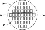
在现代的半导体封装工序中,均是将一个已经完成前段工序(Front EndProcess)的晶片10(wafer),如图1A所示;先进行薄化处理(Thinning Process),例如将芯片的厚度研磨至2~20密耳(mil)之间,如图1B所示;其中虚线105是表示每一个芯片的位置,其亦可作为后续的切割线。然后,在晶片10的主动面上形成一高分子材料层110,例如聚酰亚胺(Polyimide),使高分子材料层110覆盖主动面上的多个焊垫102,接着,以半导体的显影工序,将每一焊垫位置上的高分子材料层110移除,以形成孔洞112并曝露出每一个焊垫102,如图2A所示。然后,使用物理汽相沉积工艺(PVD)或是化学汽相沉积工艺(CVD)将一金属材料形成并填满于每一个孔洞112中,以形成一导电柱115,此导电柱115与焊垫102电性连接,如图2B所示。在本发明的一较佳实施例中,高分子材料层110的厚度可以是0.5~10密耳(mil),而导电柱115的厚度可以是0.5~3密耳(mil);同时,导电柱115的材料可以是一种硬度大的金属,例如:铜或是其它含有铜成份的合金。In the modern semiconductor packaging process, a wafer 10 (wafer) that has completed the front end process (Front End Process) is used, as shown in Figure 1A; the thinning process (Thinning Process) is first performed, such as grinding the thickness of the chip to Between 2-20 mils, as shown in FIG. 1B ; where the
接着,进行沿着虚线105对晶片进行切割(sawing process),以形成一个个的芯片100;然后,使用取放装置(pick and place)将每一个好的芯片100以覆晶的方式逐一固接在于另一个基板200的黏着层120上,以使每一个芯片的导电柱115固接于黏着层120上,如图3A所示,其中,此黏着层120为一具有弹性的黏着材料,例如硅橡胶(silicon rubber)、硅树脂(silicon resin)、弹性PU、多孔PU、丙烯酸橡胶(acrylic rubber)或芯片切割胶等。很明显地,基板200上的芯片间隔区域比晶片10中的芯片间隔区域大,因此,可以使得这些被重新放置的芯片100间具有较宽的间距,故可以将芯片100上的焊垫适当的分配。此外,本实施例所使用的封装方法,可以将12时晶片所切割出来的芯片100重新配置于8时晶片的基板上,如此可以有效运用8时晶片的即有的封装设备,而无需重新设立12时晶片的封装设备,可以降低12时晶片的封装成本。然后要强调的是,本发明的实施例并未限定使用8时晶片大小的基板,其只要能提供承载的功能者,例如:玻璃、石英、陶瓷、电路板或金属薄板(metal foil)等,均可作为本实施例的基板200,因此基板200的形状也未加以限制。Next, the wafer is cut (sawing process) along the dotted
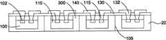
接着,请继续参考图3B,当多个包含有导电柱115的芯片100已被准确地放置并固接至基板200上的黏着层120之后,接着,于基板200及每一芯片上100的背面上形成一高分子材料层300,以使高分子材料层300填满于芯片100之间并且每一个芯片100的五个面(即除了芯片100的主动面与黏着层120接触外)均由高分子材料层300所包覆,以形成一封胶体20;其中,此高分子材料层300可以是硅胶、环氧树脂、丙烯酸(acrylic)、及苯环丁烯(BCB)等材料。然后,可以选择性地对平坦化的高分子材料层300进行一烘烤程序,以使高分子材料层300固化。此时,可以选择性地使用一种切割刀,在高分子材料层300的表面上形成多条切割道(未在图中表示),其中每一条切割道的深度为0.5~1密耳(mil),而切割道的宽度则为5至25微米。在一较佳实施例中,切割道可以选择在切割线105上,如此可以解决封胶体20产生翘曲的问题。Next, please continue to refer to FIG. 3B. After a plurality of
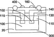
再接着,请继续参考图3C,进行基板200与高分子材料层300分离;例如将基板200与高分子材料层300一起加热或是放入去离子水的槽中,使基板200上的黏着层120与高分子材料层300剥离,形成一个以高分子材料层300包覆芯片100的封胶体20。此时,每一个芯片100主动面上的导电柱115被曝露出来;接后,再于每一个芯片100主动面上形成一高分子材料层130;再接着,以半导体的显影工序,将每一导电柱115位置上的高分子材料层130层移除,以曝露出每一个导电柱115,如图3D所示。然后,以向外延伸(fan out)技术形成多个图案化的金属线段140,每一条金属线段140的一端与导电柱115电性连接,而另一端则向外延伸形成一自由端。很明显地,此自由端不会形成在芯片100的焊垫102之上,如图3E所示。此外,金属线段140可以是由铜、金或铜合金等材料所形成,同时,金属线段140也可以是由一UBM金属层来形成,此UBM金属层的材料可以是Ti/Cu或是TiW/Cu。Then, please continue to refer to FIG. 3C to separate the
在前述将封胶体20的每一个芯片完成图案化的金属线段140后,紧接着,要进行对外连接元件的配置。如图3F所示,在封胶体20的金属线段140的面上,形成一图案化的保护层160(例如:聚酰亚胺)以覆盖多个图案化的金属线段140,并曝露出多个图案化的金属线段140的自由端。此形成图案化的保护层160的步骤包括:形成一保护层160在多个图案化的金属线段140上;利用半导体工艺,例如显影,先形成一图案化的光阻层(未在图中表示)在保护层160上;接着,在进行显影后,移除相对于多个图案化的金属线段140的向外延伸的自由端,即可曝露出每一个图案化的金属线段140的向外延伸的自由端。紧接着,在每一个曝露的自由端处形成多个导电元件400,其中导电元件400可以是锡球(solder ball)或是金属凸块(metal bump),如图3F所示。很明显地,导电元件400可以依据电路设计的需求进行配置,例如:配置成一种球阵列(BGA)的配置。After the patterned
最后,即可沿切割线105对封胶体20进行切割(sawing process),以形成一个个的完成封装的芯片100或是完成封装的模块,如图4A及图4B所示。很明显地,图4B是相对图4A的沿CC线段的剖视图。Finally, the sealing
在上述实施例中,包覆每一个芯片100的高分子材料层300的方式可以选择使用已知的机械压膜(stamping process)或是注模方式(molding process)来形成。此外,由于本发明在将基板200与封胶体20分离后,使得每一芯片100的主动面的导电柱115都曝露出来,故可解决后续进行金属线连接时的对准问题。基于此对准问题的解决,故依据本发明所揭露的方式,可将多个相同或是不相同的好的芯片100封装在一起,然后采用半导体工艺来形成图案化的金属线400,将所要组合成模块(MODULE)的多个芯片100电性连接在一起。例如:将4个256M的DRAM芯片以串连或并连的方式封装在一起,形成一个存储容量为1G的存储模块;或是,将多个发光二极管(LED)串接成一个柱状光源或是并连成一面状光源;或是,将不同功能、不同大小的芯片封装成一系统等,都可通过本实施例来达成。In the above embodiments, the
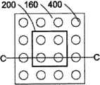
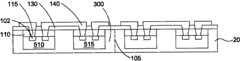
图5是显示本发明的系统级封装(System-In-Package;SIP)的上视图。当多个晶片所制造出的多个具有不同功能的芯片,例如:芯片505为一微处理装置、芯片510为一存储器控制装置而芯片515为一个存储器装置装置;将上述不同功能的芯片依据前述工序(即完成导电柱115工序)并将每一个不同功能及尺寸的芯片放置于另一基板200上之后,可通过图3A至图3F的过程,将这些不同功能的芯片(包括芯片505、芯片510及芯片515)形成一封胶体20,然后,将基板200与封胶体20分离后,可以使得封胶体20上的多个不同功能的芯片(包括芯片505、芯片510及芯片515)中的每一导电柱115曝露出来。在此要强调,本发明通过覆晶的工序,使用每一个不同功能及尺寸的芯片的导电柱115位于同一平面上,故当基板200与封胶体20分离后,封胶体20上的导电柱115能够曝露在同一平面上。故可以有效地解决对准的问题。FIG. 5 is a top view showing a System-In-Package (SIP) of the present invention. When a plurality of chips with different functions produced by a plurality of wafers, for example: chip 505 is a microprocessing device,
然后,再于封胶体20上形成一高分子材料层130;再接着,以半导体的显影工序,将每一导电柱115位置上的高分子材料层130层移除,以曝露出每一个导电柱115;再接着,使用一电镀工序,以便在高分子材料层300上形成一金属层(未显示于图中),同时金属层与每一个导电柱115形成电性连接。接着,利用半导体工艺,例如:以涂布、显影及蚀刻等方式,先形成一图案化光阻层(未在图中表示)在金属层之上;然后以蚀刻方式来移除部份金属层之后,再剥除图案化的光阻层;因此,可以依据所需要的电性连接方式来形成多个图案化的金属线段140;而在本实施例中,每一图案化的金属线段140的向外延伸的两端是电性连接至相邻的每一芯片上的多个导电柱115,使得相邻的每一芯片彼此是以串联或并联的方式电性连接成一系统,如图6A所示;在此要说明的是,此串联或并联的电性连接方式仅为本发明的一实施例,其目的仅在揭露使用图案化的金属工艺,可以将多个芯片依据所要的电性连接方式完成连接。Then, a
在前述将封胶体20的多个芯片以金属线段140完成系统化的电性连接后,紧接着,要进行对外连接元件400的配置,其过程与图3E至图3F的过程相同,故其相关过程不再予以重复赘述。很明显地,导电元件400可以是锡球(solder ball)或是金属凸块(metal bump)。同时,导电元件400可以依据电路设计的需求进行配置,例如:配置成一种球阵列(BGA)的配置,如图6B所示。最后,即可依据切割线105切割封胶体20,以形成多个完成封装的模块,如图7所示。After completing the systematic electrical connection of the plurality of chips of the
很明显地,当封胶体20中的多个芯片是相同功能及相同大小的芯片;例如:LED;其同样地可以使用金属线段140将多个芯片以串联或并联方式形成一模块(module),金属线段140可以是由铜、金或铜合金等材料所形成,同时,金属线段140也可以是由一UBM金属层来形成,此UBM金属层的材料可以是Ti/Cu或是TiW/Cu。Obviously, when the multiple chips in the
当所要封装的多个芯片为发光二极管(LED)时,即可将每一发光二极管的P电极与相邻的发光二极管的P电极电性连接;而发光二极管的N电极是与相邻的发光二极管的N电极电性连接,且每一发光二极管的N电极及P电极是通过导电柱115分别金属线段140电性连接。同样地,本发明也不限定发光二极管的数量或是其电性连接的方式,例如:将多个发光二极管(LED)串接成一个柱状光源或是并连成一面状光源;同时,本发明也不限定发光二极管的发光颜色,即发光二极管可以是红光发光二极管或绿光发光二极管或蓝光发光二极管或其它颜色的发光二极管(例如:白光)或是前述发光二极管的组合等。最后,如图3E至图3F过程,于曝露的金属线段140的自由端上形成导电元件400。When the multiple chips to be packaged are light emitting diodes (LEDs), the P electrode of each light emitting diode can be electrically connected to the P electrode of the adjacent light emitting diode; and the N electrode of the light emitting diode is connected to the adjacent light emitting diode. The N electrodes of the diodes are electrically connected, and the N electrodes and the P electrodes of each LED are electrically connected through the
而当封胶体20中的多个芯片是相同功能及相同大小的芯片均无DRAM时;例如:将4个256M的DRAM芯片以串连或并连的方式封装在一起时,其同样地可以使用金属线段140将多个芯片以串联或并联方式形成一个存储容量为1G的存储模块。由于形成金属线段140及导电元件400的过程与前述相同,故不再重复赘述。And when a plurality of chips in the
虽然本发明以前述的较佳实施例揭露如上,然而其并非用以限定本发明,任何熟悉本技术的普通技术人员,在不脱离本发明的精神和范围内,当可作出种种等同的改变或替换,因此本发明的专利保护范围须视本说明书所附的本申请权利要求范围所界定的为准。Although the present invention is disclosed above with the foregoing preferred embodiments, it is not intended to limit the present invention. Any person familiar with the art may make various equivalent changes or changes without departing from the spirit and scope of the present invention. Therefore, the scope of patent protection of the present invention must be defined by the scope of the claims of the application attached to this specification.
Claims (10)
Translated fromChinesePriority Applications (1)
| Application Number | Priority Date | Filing Date | Title |
|---|---|---|---|
| CNA2008101102740ACN101609822A (en) | 2008-06-19 | 2008-06-19 | Package structure for chip reconfiguration and method thereof |
Applications Claiming Priority (1)
| Application Number | Priority Date | Filing Date | Title |
|---|---|---|---|
| CNA2008101102740ACN101609822A (en) | 2008-06-19 | 2008-06-19 | Package structure for chip reconfiguration and method thereof |
Publications (1)
| Publication Number | Publication Date |
|---|---|
| CN101609822Atrue CN101609822A (en) | 2009-12-23 |
Family
ID=41483501
Family Applications (1)
| Application Number | Title | Priority Date | Filing Date |
|---|---|---|---|
| CNA2008101102740APendingCN101609822A (en) | 2008-06-19 | 2008-06-19 | Package structure for chip reconfiguration and method thereof |
Country Status (1)
| Country | Link |
|---|---|
| CN (1) | CN101609822A (en) |
Cited By (5)
| Publication number | Priority date | Publication date | Assignee | Title |
|---|---|---|---|---|
| CN103107103A (en)* | 2011-11-11 | 2013-05-15 | 北京大学深圳研究生院 | Reconfigurable operator array structure scale extension method based on wafer level packaging (WLP) form |
| CN105390595A (en)* | 2015-12-01 | 2016-03-09 | 广州市信自达电子科技有限公司 | Preparation method for unidirectional white light component of high color gradation consistency |
| CN108242405A (en)* | 2016-12-27 | 2018-07-03 | 冠宝科技股份有限公司 | Substrate-free semiconductor package manufacturing method |
| CN110676181A (en)* | 2019-09-23 | 2020-01-10 | 上海朕芯微电子科技有限公司 | Diffusion type CSP packaging method |
| CN110741471A (en)* | 2017-06-23 | 2020-01-31 | 应用材料公司 | Method of redistribution layer formation for advanced packaging applications |
- 2008
- 2008-06-19CNCNA2008101102740Apatent/CN101609822A/enactivePending
Cited By (6)
| Publication number | Priority date | Publication date | Assignee | Title |
|---|---|---|---|---|
| CN103107103A (en)* | 2011-11-11 | 2013-05-15 | 北京大学深圳研究生院 | Reconfigurable operator array structure scale extension method based on wafer level packaging (WLP) form |
| CN105390595A (en)* | 2015-12-01 | 2016-03-09 | 广州市信自达电子科技有限公司 | Preparation method for unidirectional white light component of high color gradation consistency |
| CN108242405A (en)* | 2016-12-27 | 2018-07-03 | 冠宝科技股份有限公司 | Substrate-free semiconductor package manufacturing method |
| CN110741471A (en)* | 2017-06-23 | 2020-01-31 | 应用材料公司 | Method of redistribution layer formation for advanced packaging applications |
| CN110741471B (en)* | 2017-06-23 | 2023-10-20 | 应用材料公司 | Method of redistribution layer formation for advanced packaging applications |
| CN110676181A (en)* | 2019-09-23 | 2020-01-10 | 上海朕芯微电子科技有限公司 | Diffusion type CSP packaging method |
Similar Documents
| Publication | Publication Date | Title |
|---|---|---|
| TWI387077B (en) | Grain reconfigurable package structure and method thereof | |
| TWI700753B (en) | Chip package and method for forming the same | |
| US7888172B2 (en) | Chip stacked structure and the forming method | |
| CN101621041B (en) | Package structure and method for chip reconfiguration | |
| US7326592B2 (en) | Stacked die package | |
| CN101232008A (en) | Multi-die packaging and method thereof | |
| US7679178B2 (en) | Semiconductor package on which a semiconductor device can be stacked and fabrication method thereof | |
| US20110209908A1 (en) | Conductor package structure and method of the same | |
| US20090160043A1 (en) | Dice Rearrangement Package Structure Using Layout Process to Form a Compliant Configuration | |
| TWI387014B (en) | Die reconfiguration structure with sacrificial substrate and packaging method thereof | |
| CN101197356A (en) | Multi-chip packaging structure and forming method thereof | |
| JP2008244437A (en) | Image sensor package with die receiving opening and method thereof | |
| CN101252125A (en) | Multiple crystal grain packaging structure with reducing structure and its forming method | |
| CN101477956B (en) | Small chip reconfiguration packaging structure and packaging method | |
| CN101477955B (en) | Small chip reconfiguration packaging structure and packaging method | |
| US20160307878A1 (en) | Reconstituted wafer-level package dram | |
| CN101567322B (en) | Chip packaging structure and packaging method thereof | |
| CN101615583A (en) | Chip stack structure and method of forming the same | |
| JP2005079489A (en) | Semiconductor device | |
| CN101609822A (en) | Package structure for chip reconfiguration and method thereof | |
| US20110031607A1 (en) | Conductor package structure and method of the same | |
| US11670600B2 (en) | Panel level metal wall grids array for integrated circuit packaging | |
| CN101452862B (en) | Packaging method for die reconfiguration | |
| CN101266966B (en) | Multi-chip package module and manufacturing method thereof | |
| CN100590823C (en) | Method for manufacturing alignment mark used in packaging structure with reconfigured crystal grains |
Legal Events
| Date | Code | Title | Description |
|---|---|---|---|
| C06 | Publication | ||
| PB01 | Publication | ||
| C10 | Entry into substantive examination | ||
| SE01 | Entry into force of request for substantive examination | ||
| C02 | Deemed withdrawal of patent application after publication (patent law 2001) | ||
| WD01 | Invention patent application deemed withdrawn after publication | Open date:20091223 |