CN101609063A - A microelectrode array chip sensor for electrochemical immunoassay - Google Patents
A microelectrode array chip sensor for electrochemical immunoassayDownload PDFInfo
- Publication number
- CN101609063A CN101609063ACNA2009100548867ACN200910054886ACN101609063ACN 101609063 ACN101609063 ACN 101609063ACN A2009100548867 ACNA2009100548867 ACN A2009100548867ACN 200910054886 ACN200910054886 ACN 200910054886ACN 101609063 ACN101609063 ACN 101609063A
- Authority
- CN
- China
- Prior art keywords
- electrode
- chip
- working electrode
- auxiliary electrode
- working
- Prior art date
- Legal status (The legal status is an assumption and is not a legal conclusion. Google has not performed a legal analysis and makes no representation as to the accuracy of the status listed.)
- Granted
Links
Images
Landscapes
- Apparatus Associated With Microorganisms And Enzymes (AREA)
- Investigating Or Analysing Biological Materials (AREA)
Abstract
Translated fromChinese
Description
Translated fromChinese技术领域technical field
本发明属于传感器技术领域,具体涉及一种用于电化学生物免疫检测的微电极集成阵列芯片传感器。The invention belongs to the technical field of sensors, and in particular relates to a microelectrode integrated array chip sensor for electrochemical biological immune detection.
背景技术Background technique
电化学检测方法是利用电极将不同物质发生的生化反应产生的信号转换成电信号,从而确定物质间进行反映的微观过程,物质含量等。根据电化学检测原理的不同可以分为电流法、电位法、电导法等。自电化学的方法发明以来,经过不断地发展,对电极与溶液界面的特性研究已经具有了非常好的理论基础,电化学检测可以应用于无机离子、有机离子、蛋白质、氨基酸、DNA等分析物。这也是此方法可以广泛用于生物传感器的原因。The electrochemical detection method is to use electrodes to convert the signals generated by the biochemical reactions of different substances into electrical signals, so as to determine the microscopic process of reflection between substances, the content of substances, etc. According to different electrochemical detection principles, it can be divided into current method, potentiometric method, conductometric method and so on. Since the invention of the electrochemical method, through continuous development, the research on the characteristics of the interface between the electrode and the solution has had a very good theoretical basis. Electrochemical detection can be applied to analytes such as inorganic ions, organic ions, proteins, amino acids, and DNA. . This is why this method can be widely used in biosensors.
生物传感器是在化学传感器的基础上发展起来的,它是由产生信号的敏感元件(分子识别元件)和信号转换器件组成。生物传感器的发展始于1962年,当时L.c.clark将电极与含有葡萄糖氧化酶的膜结合应用于葡萄糖检测。随后其应用领域不断扩展,检测方法也不断改进。根据检测物质的不同,可分为免疫传感器、DNA传感器、酶传感器、细胞传感器等几类。Biosensors are developed on the basis of chemical sensors, which are composed of sensitive elements (molecular recognition elements) that generate signals and signal conversion devices. The development of biosensors began in 1962 when L.c. clark combined electrodes with membranes containing glucose oxidase for glucose detection. Subsequently, its application fields have been continuously expanded, and detection methods have been continuously improved. According to different detection substances, it can be divided into several categories such as immunosensors, DNA sensors, enzyme sensors, and cell sensors.
最近二三十年里,微机电系统(MEMS)加工技术的发展使生物传感器及其生化分析仪器进一步向小型化、数字化和高可靠性的方向发展。随着生物技术的日臻完善、微电子学技术的迅速发展以及实际应用领域的迫切要求,作为一种多学科交叉的高技术、作为一种强有力的分析工具,生物传感器已成功地应用于医学、国防、环境、食品工业及农业等领域。In the last 20 to 30 years, the development of microelectromechanical system (MEMS) processing technology has further developed biosensors and biochemical analysis instruments in the direction of miniaturization, digitization and high reliability. With the improvement of biotechnology, the rapid development of microelectronics technology and the urgent requirements of practical applications, biosensors, as a multidisciplinary high technology and a powerful analytical tool, have been successfully used in medicine. , national defense, environment, food industry and agriculture and other fields.
微机电系统(MEMS)技术对电化学生物传感器的最主要影响是电极的改进,电极的尺寸有原来的常规电极发展到了微电极。传统分别使用的三电极系统电极(参比电极、辅助电极、工作电极)可以集成于一个芯片上;一个传感器器件上就可以集成多个具有独立检测功能的电极,从而实现了一个器件可以同时检测多种生物样品。微电极不仅仅具有小型化的优点,更重要的是它与常规电极相比具有无可比拟的优点,即极高的稳态电流密度、极短的响应时间、极化电流小、传质速率高、信噪比大等特点。The most important influence of microelectromechanical systems (MEMS) technology on electrochemical biosensors is the improvement of electrodes, and the size of electrodes has been developed from conventional electrodes to microelectrodes. Traditionally used three-electrode system electrodes (reference electrode, auxiliary electrode, working electrode) can be integrated on one chip; multiple electrodes with independent detection functions can be integrated on one sensor device, so that one device can simultaneously detect various biological samples. Microelectrode not only has the advantages of miniaturization, but more importantly, it has incomparable advantages compared with conventional electrodes, that is, extremely high steady-state current density, extremely short response time, small polarization current, and mass transfer rate. High, high signal-to-noise ratio and so on.
目前对微电极的研究方向是制造一种具有高稳定性,高响应特性,可重复性高的电极。用于电化学检测的三个电极全部集成制造于一个芯片上,对于检测的稳定性具有非常重要的意义。减小工作电极与辅助电极的距离也成为了一种增加响应特性的主要趋势。使用Ag/AgCl作为参比电极,利用MEMS工艺集成于同一个器件之中,提高稳定性、可重复性非常关键。同时制造多个电极,并且以某一结构进行阵列分布对于检测相应特性的提高有着许多报道和尝试。另外对于电极形状的探讨一直在进行。The current research direction of microelectrodes is to manufacture an electrode with high stability, high response characteristics and high repeatability. The three electrodes used for electrochemical detection are all integrated and manufactured on one chip, which is very important for the stability of detection. Reducing the distance between the working electrode and the auxiliary electrode has also become a major trend to increase the response characteristics. Using Ag/AgCl as a reference electrode and integrating it into the same device using MEMS technology is very important to improve stability and repeatability. There are many reports and attempts to fabricate multiple electrodes at the same time and distribute them in a certain structure to improve the corresponding characteristics. In addition, discussions on electrode shapes have been ongoing.
由于集成电化学传感器参比电极和辅助电极引入,必然要考虑其形状,面积的影响。在电化学基本理论中,介绍到当工作电极和辅助电极在彼此分开的电解池时,辅助电极一侧的反应基本可以忽略不计。但是,当工作电极和辅助电极同处一个电解池时,辅助电极一侧的反应生成物将严重影响工作电极的反应。并指出,不用恒电位的电解反应中,希望辅助电极面积比工作电极面积大很多,外部加的极化作用主要作用于工作电极上。F.Lisdat.D.在《Analytical and Bioanalytical Chemistry》杂志发表的《The use ofelectrochemical impedance spectroscopy for biosensing》(2008年4月16日)也指出辅助电极面积要远大于工作电极的面积。张祖训在杂志《电分析化学进展》发表的《微电极电化学模拟新方法有限分析法》通过模拟的方法指出微环电极的电流密度高于圆盘电极。Due to the introduction of the reference electrode and auxiliary electrode of the integrated electrochemical sensor, the influence of its shape and area must be considered. In the basic theory of electrochemistry, it is introduced that when the working electrode and the auxiliary electrode are separated from each other in the electrolytic cell, the reaction on the side of the auxiliary electrode is basically negligible. However, when the working electrode and the auxiliary electrode are in the same electrolytic cell, the reaction products on the side of the auxiliary electrode will seriously affect the reaction of the working electrode. It is also pointed out that in the electrolytic reaction without constant potential, it is desirable that the area of the auxiliary electrode is much larger than that of the working electrode, and the external polarization mainly acts on the working electrode. F. Lisdat. D. "The use of electrochemical impedance spectroscopy for biosensing" (April 16, 2008) published in the journal "Analytical and Bioanalytical Chemistry" also pointed out that the area of the auxiliary electrode should be much larger than that of the working electrode. Zhang Zuxun's "Limited Analysis Method for Microelectrode Electrochemical Simulation New Method" published in the journal "Progress in Electroanalytical Chemistry" pointed out that the current density of the micro-ring electrode is higher than that of the disc electrode through the simulation method.
于是,在目前MEMS工艺的基础上,设计制造一种具有如下特点的生物芯片将具有非常大的意义。工作电极,辅助电极,参比电极集成于一个芯片;增加辅助电极相对于工作电极的面积;辅助电极与工作电极结构为环形结构。Therefore, on the basis of the current MEMS technology, it will be of great significance to design and manufacture a biochip with the following characteristics. The working electrode, the auxiliary electrode, and the reference electrode are integrated into one chip; the area of the auxiliary electrode relative to the working electrode is increased; the auxiliary electrode and the working electrode have a ring structure.
发明内容Contents of the invention
本发明的目的在于提出一种响应特征明显,电化学特性稳定,生物匹配性良好的用于电化学免疫检测的微电极芯片传感器。The purpose of the present invention is to provide a microelectrode chip sensor for electrochemical immunodetection with obvious response characteristics, stable electrochemical characteristics and good biological matching.
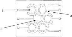
本发明提出的用于电化学免疫检测的微电极芯片传感器,是利用现有MEMS工艺技术的制备条件,设计了一种新的电极结构。该芯片集成了电化学检测使用的三种电极,即工作电极、辅助电极和参比电极。这三种电极通过MEMS工艺制作于同一个芯片上,其结构如图1所示。工作电极为目前使用最为成熟的圆盘电极,工作电极由具有良好生物相容性的Au材料制作。芯片中制作了多个工作电极,按照一定规则成阵列分布。辅助电极为与工作电极同心的几端环弧相连构成,辅助电极的面积对于整个芯片的响应特性产生影响,相对于工作电极而言面积较大的辅助电极可以使芯片工作更加稳定,但是对于同一个芯片而言,辅助电极面积的增大必然会使工作电极的面积减小,可能会造成检测信号变弱的问题。因此,辅助电极面积应根据工作电极的大小和检测的样品特性来确定。辅助电极的材料可以使用Au或者Pt。参比电极位于整个芯片的中心位置,参比电极为星形,其边界有多端弧形边界组成,并且参比电极的边界与辅助电极的边界平行(即两边界在各点的法线方向上的距离相等),参比电极的边界与辅助电极的边界距离为100μm~200μm,参比电极使用Ag/AgCl制作完成。The micro-electrode chip sensor for electrochemical immunodetection proposed by the present invention uses the preparation conditions of the existing MEMS technology to design a new electrode structure. The chip integrates three electrodes used in electrochemical detection, namely working electrode, auxiliary electrode and reference electrode. These three kinds of electrodes are fabricated on the same chip by MEMS process, and its structure is shown in Fig. 1 . The working electrode is the most mature disc electrode currently used, and the working electrode is made of Au material with good biocompatibility. Multiple working electrodes are fabricated in the chip and distributed in an array according to certain rules. The auxiliary electrode is composed of several concentric ring arcs connected with the working electrode. The area of the auxiliary electrode has an impact on the response characteristics of the entire chip. Compared with the working electrode, the auxiliary electrode with a larger area can make the chip work more stable, but for the same As far as a chip is concerned, the increase in the area of the auxiliary electrode will inevitably reduce the area of the working electrode, which may cause the problem of weakening of the detection signal. Therefore, the area of the auxiliary electrode should be determined according to the size of the working electrode and the characteristics of the sample to be detected. Au or Pt can be used as the material of the auxiliary electrode. The reference electrode is located at the center of the entire chip. The reference electrode is star-shaped, and its boundary is composed of multi-terminal arc boundaries, and the boundary of the reference electrode is parallel to the boundary of the auxiliary electrode (that is, the two boundaries are in the normal direction of each point. distances are equal), the distance between the boundary of the reference electrode and the boundary of the auxiliary electrode is 100 μm to 200 μm, and the reference electrode is made of Ag/AgCl.
本发明中,工作电极在芯片中成阵列分布,所有工作电极的圆心在以芯片中心为圆心的圆的边界上;根据测试的不同可以决定工作电极的数目,工作电极按一定角度在芯片上均匀分布,电极的数目可以为3~5个。工作电极的大小根据不同测试的需要、不同的工艺条件,以及芯片的大小等进行确定,本发明的工作电极半径在200μm~600μm范围内选择。In the present invention, the working electrodes are distributed in an array in the chip, and the centers of all working electrodes are on the boundary of a circle centered on the center of the chip; the number of working electrodes can be determined according to different tests, and the working electrodes are evenly distributed on the chip at a certain angle. distribution, the number of electrodes can be 3-5. The size of the working electrode is determined according to the needs of different tests, different process conditions, and the size of the chip. The radius of the working electrode in the present invention is selected within the range of 200 μm to 600 μm.
辅助电极在一个芯片中仅为一个,由多个以工作电极为圆心的环弧相连构成,且包围了工作电极。在设计中,为了有效利用芯片面积,使得相邻间的环弧有重叠部分,这些重叠部分使得辅助电极构成了一个整体,辅助电极的面积大小的控制主要通过改变环弧半径的大小来实现,使用100μm~500μm的环弧半径对于芯片的稳定工作具有很好的作用。There is only one auxiliary electrode in a chip, which is composed of multiple ring arcs with the working electrode as the center, and surrounds the working electrode. In the design, in order to effectively use the chip area, the adjacent circular arcs have overlapping parts. These overlapping parts make the auxiliary electrodes form a whole. The control of the area of the auxiliary electrodes is mainly realized by changing the radius of the circular arcs. The use of a ring arc radius of 100 μm to 500 μm has a good effect on the stable operation of the chip.
辅助电极环弧内侧与对应的工作电极圆盘边缘间的距离对于电化学检测的灵敏度具有重要的影响,距离越小,灵敏度越高。但是加工工艺要求越高。本发明采用的距离为50μm~200μm。The distance between the inner side of the auxiliary electrode ring arc and the corresponding edge of the working electrode disc has an important impact on the sensitivity of electrochemical detection, the smaller the distance, the higher the sensitivity. But the processing technology requirements are higher. The distance used in the present invention is 50 μm to 200 μm.
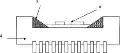
芯片上的三种电极由各自的电极导线引出。芯片通过封装,与陶瓷底座一起构成传感器,通过硅胶封装导线,同时硅胶沿着芯片边缘封装与底部的阵列芯片构成凹槽,作为微电极芯片传感器的检测池(电解池)。该发明使用了集成芯片,不需要外加电极,保证了测量的稳定性。The three kinds of electrodes on the chip are led out by their respective electrode wires. The chip is packaged to form a sensor with the ceramic base, and the wire is packaged with silica gel. At the same time, the silica gel is packaged along the edge of the chip and forms a groove with the array chip at the bottom, which is used as the detection cell (electrolytic cell) of the microelectrode chip sensor. The invention uses an integrated chip, does not require external electrodes, and ensures the stability of the measurement.
上述微电极阵列芯片传感器制作采用微电子机械加工技术(MEMS),本发明通过以下具体步骤来实现:Above-mentioned microelectrode array chip sensor is made and adopts microelectron machining technology (MEMS), and the present invention realizes through following concrete steps:
1.在P型硅衬底上热氧化生长二氧化硅,作为绝缘层。1. Thermally oxidize and grow silicon dioxide on a P-type silicon substrate as an insulating layer.
2.使用piranha溶液(H2SO4∶H2O2=3∶1)清洗二氧化硅表面,去离子水清洗去除杂质,烘干硅片;光刻,使用正胶形成工作电极图形。氧等离子体溅射打底膜。2. Use piranha solution (H2 SO4 :H 2 O2 =3:1) to clean the silicon dioxide surface, wash with deionized water to remove impurities, and dry the silicon wafer; photolithography, use positive resist to form working electrode patterns. Oxygen plasma sputtering base film.
3.溅射PVD Ti作为电极的粘附层,溅射Au作为工作电极;采用lift-off工艺去除光刻胶形成工作电极图形。3. Sputter PVD Ti as the adhesion layer of the electrode, and sputter Au as the working electrode; use the lift-off process to remove the photoresist to form the working electrode pattern.
4.光刻,使用正胶形成辅助电极图形,氧等离子体溅射打底膜,溅射PVD Ti作为电极粘附层,溅射PVD Au或者Pt作为辅助电极,lift-off工艺去除光刻胶,形成辅助电极图形。4. Photolithography, using positive resist to form auxiliary electrode pattern, oxygen plasma sputtering base film, sputtering PVD Ti as electrode adhesion layer, sputtering PVD Au or Pt as auxiliary electrode, lift-off process to remove photoresist , forming an auxiliary electrode pattern.
5.光刻,使用正胶形成参比电极图形,氧等离子体溅射打底膜,溅射PVD Ti作为粘附层,溅射PVDAg作为参比电极,lift-off工艺去除光刻胶,形成参比电极图形。5. Photolithography, using positive resist to form reference electrode pattern, oxygen plasma sputtering base film, sputtering PVD Ti as adhesion layer, sputtering PVDAg as reference electrode, lift-off process to remove photoresist, forming Reference electrode pattern.
6.划片,打线,硅胶封装。待硅胶凝固后,电解池加盐酸,参比电极加正电压,电解液加负电压构成直流通路,通过电化学反应在Ag表面形成AgCl,参比电极制作完成,传感器制作完成。6. Dicing, wire bonding, silicone encapsulation. After the silica gel is solidified, hydrochloric acid is added to the electrolytic cell, a positive voltage is applied to the reference electrode, and a negative voltage is applied to the electrolyte to form a direct current path. AgCl is formed on the surface of Ag through an electrochemical reaction, and the reference electrode and sensor are completed.
本发明的制得的电化学三电极集成芯片集成了电化学使用的三种电极于一体,避免了外加电极带来的干扰,极大的提高了电化学检测的信噪比,增强了电化学检测的稳定性。对于器件的使用操作进行了很大的简化,提高了器件的便携性,有利于器件的产品化。The prepared electrochemical three-electrode integrated chip of the present invention integrates three kinds of electrodes used in electrochemistry, avoids the interference caused by external electrodes, greatly improves the signal-to-noise ratio of electrochemical detection, and enhances the electrochemical Detection stability. The use and operation of the device is greatly simplified, the portability of the device is improved, and the productization of the device is facilitated.
本发明工作电极可以根据检测的需要进行多通道检测,可以对多种样品同时进行检测,极大地提高了检测的效率。The working electrode of the present invention can perform multi-channel detection according to detection requirements, and can simultaneously detect various samples, thereby greatly improving detection efficiency.
本发明制作的环形辅助电极相比传统的圆形电极具有更高的响应电流,辅助电极的面积增加,对于提高器件的稳定性具有非常重要的帮助。环形电极的设计也使得芯片的有效利用面积得到了增强。Compared with the traditional circular electrode, the ring-shaped auxiliary electrode produced by the present invention has a higher response current, and the area of the auxiliary electrode is increased, which is very important for improving the stability of the device. The design of the ring electrode also enhances the effective utilization area of the chip.
本发明在工艺条件内,对辅助电极和工作电极的距离进行减小,提高了电化学检测的精度。The invention reduces the distance between the auxiliary electrode and the working electrode within the technological conditions, and improves the precision of electrochemical detection.
本发明使用陶瓷底座进行封装,使用绝缘硅胶进行封装,一方面保证了封装的绝缘性能,另一方面硅胶与电化学三电极集成芯片构成电解池,为检测工作带来了很大的方便。The invention uses a ceramic base for packaging and uses insulating silica gel for packaging. On the one hand, the insulation performance of the package is guaranteed. On the other hand, the silica gel and electrochemical three-electrode integrated chip form an electrolytic cell, which brings great convenience to the detection work.
附图说明Description of drawings
图1为电极形状图形Figure 1 is the electrode shape graph
图2为传感器器件结构Figure 2 shows the structure of the sensor device
图中标号:1是工作电极,2是辅助电极,3是参比电极,4是陶瓷底座,5是封装硅胶,6为芯片。Numbers in the figure: 1 is the working electrode, 2 is the auxiliary electrode, 3 is the reference electrode, 4 is the ceramic base, 5 is the packaging silica gel, and 6 is the chip.
具体实施方式Detailed ways
下面结合附图和实施例对本发明作进一步说明。实施例在以本发明方案为技术前提下,给出了详细的实施方案和具体操作过程,但本发明的保护范围不限于实施例。The present invention will be further described below in conjunction with drawings and embodiments. EXAMPLES On the technical premise of the solution of the present invention, detailed implementation and specific operation process are given, but the scope of protection of the present invention is not limited to the examples.
1.在P型硅衬底上热氧化生长600nm的二氧化硅,作为绝缘层。1. Thermally oxidize and grow 600nm silicon dioxide on a P-type silicon substrate as an insulating layer.
2.使用piranha溶液(H2SO4∶H2O2=3∶1)清洗二氧化硅表面,去离子水清洗去除杂质,烘干硅片;光刻,使用正胶形成工作电极图形,工作电极半径为500μm。氧等离子体溅射打底膜。2. Use piranha solution (H2 SO4 :H 2 O2 = 3: 1) to clean the surface of silicon dioxide, wash with deionized water to remove impurities, and dry the silicon wafer; photolithography, use positive resist to form a working electrode pattern, and work The electrode radius is 500 μm. Oxygen plasma sputtering base film.
3.溅射PVD 20nm的Ti,300nm的Au;采用lift-off工艺去除光刻胶形成工作电极图形,工作电极半径为500μm。3. Sputter PVD 20nm Ti and 300nm Au; use lift-off process to remove photoresist to form working electrode pattern, working electrode radius is 500μm.
4.光刻,使用正胶形成辅助电极图形,氧等离子体溅射打底膜,溅射PVD 20nm Ti,300nm Pt,lift-off工艺去除光刻胶,形成辅助电极图,形辅助电极的环径为200μm,辅助电极与工作电极的距离为100μm。4. Photolithography, use positive resist to form auxiliary electrode pattern, oxygen plasma sputtering base film, sputter PVD 20nm Ti, 300nm Pt, lift-off process to remove photoresist, form auxiliary electrode pattern, and shape auxiliary electrode ring The diameter is 200 μm, and the distance between the auxiliary electrode and the working electrode is 100 μm.
5.光刻,使用正胶形成参比电极图形,氧等离子体溅射打底膜,溅射PVD 20nm Ti,400nmAg,lift-off工艺去除光刻胶,形成参比电极图形,参比电极的边界与辅助电极边界的距离为100μm。5. Photolithography, use positive resist to form reference electrode pattern, oxygen plasma sputtering base film, sputter PVD 20nm Ti, 400nmAg, lift-off process to remove photoresist, form reference electrode pattern, reference electrode The distance between the boundary and the auxiliary electrode boundary is 100 μm.
6.划片,打线,硅胶封装。待硅胶凝固后,电解池加盐酸,参电极加正电压0.5V,电解液加负电压构成直流通路,通电5s,通过电化学反应在Ag表面形成AgCl,参电极制作完成,传感器制作完成。6. Dicing, wire bonding, silicone encapsulation. After the silica gel is solidified, add hydrochloric acid to the electrolytic cell, add a positive voltage of 0.5V to the reference electrode, and add a negative voltage to the electrolyte to form a direct current path. After energizing for 5s, AgCl is formed on the Ag surface through an electrochemical reaction. The reference electrode and sensor are completed.
传感器制作完成后,使用电化学分析仪,采用循环伏安法进行测试,对封装完成的芯片进行裸电极的测试。电化学分析仪辅助电极和工作电极连线分别与传感器芯片的辅助电极和工作电极相连构成通路,参比电极导线与连接芯片参比电极提供基准电压。在传感器的电解池中加入10mM PBS溶液和10mM二茂铁甲醇的混合溶液,PBS为支持电介质,二茂铁甲醇为探针。以0.1V/s,在-0.5V~0.5V进行扫描,测得循环伏安曲线。对本发明的传感器进行测试,得到氧化峰的峰值为3.43μA,还原峰的峰值为3.34μA,通过计算可以得到其峰值电流密度分别为0.437mA/cm2和0.425mA/cm2。说明该传感器具有较高的灵敏度。After the sensor is fabricated, the electrochemical analyzer is used to test by cyclic voltammetry, and the packaged chip is tested on the bare electrode. The auxiliary electrode and the working electrode of the electrochemical analyzer are respectively connected to the auxiliary electrode and the working electrode of the sensor chip to form a path, and the reference electrode wire is connected to the reference electrode of the chip to provide a reference voltage. A mixed solution of 10 mM PBS solution and 10 mM ferrocenemethanol was added to the electrolytic cell of the sensor, PBS was used as a supporting dielectric, and ferrocenemethanol was used as a probe. Scan at -0.5V to 0.5V at 0.1V/s, and measure the cyclic voltammetry curve. The sensor of the present invention is tested, and the peak value of the oxidation peak is 3.43 μA, and the peak value of the reduction peak is 3.34 μA, and the peak current densities thereof are respectively 0.437 mA/cm2 and 0.425 mA/cm2 through calculation. It shows that the sensor has high sensitivity.
本发明可以用于生物医药等多领域的各种样品的检测。本发明可以通过电化学原位共沉积的的方法将抗体包埋于电聚合的膜中,从而可以用于不同目标检测的芯片传感器。也可以制备聚邻苯二胺绝缘膜包埋的抗体部分绝缘膜进行电化学分析。或者采用自组装分子的方法将抗体固定到工作电极,从而构成具有不同检测目的的生物传感器。The invention can be used for detection of various samples in various fields such as biomedicine. The present invention can embed the antibody in the electropolymerized membrane through the method of electrochemical in-situ co-deposition, so that it can be used for chip sensors for different target detection. It is also possible to prepare poly-o-phenylenediamine insulating film-embedded antibody partial insulating film for electrochemical analysis. Alternatively, antibodies can be fixed to the working electrode by self-assembled molecules to form biosensors with different detection purposes.
Claims (3)
Priority Applications (1)
| Application Number | Priority Date | Filing Date | Title |
|---|---|---|---|
| CN200910054886.7ACN101609063B (en) | 2009-07-16 | 2009-07-16 | A microelectrode array chip sensor for electrochemical immunoassay |
Applications Claiming Priority (1)
| Application Number | Priority Date | Filing Date | Title |
|---|---|---|---|
| CN200910054886.7ACN101609063B (en) | 2009-07-16 | 2009-07-16 | A microelectrode array chip sensor for electrochemical immunoassay |
Publications (2)
| Publication Number | Publication Date |
|---|---|
| CN101609063Atrue CN101609063A (en) | 2009-12-23 |
| CN101609063B CN101609063B (en) | 2014-01-08 |
Family
ID=41482892
Family Applications (1)
| Application Number | Title | Priority Date | Filing Date |
|---|---|---|---|
| CN200910054886.7AExpired - Fee RelatedCN101609063B (en) | 2009-07-16 | 2009-07-16 | A microelectrode array chip sensor for electrochemical immunoassay |
Country Status (1)
| Country | Link |
|---|---|
| CN (1) | CN101609063B (en) |
Cited By (29)
| Publication number | Priority date | Publication date | Assignee | Title |
|---|---|---|---|---|
| CN102095770A (en)* | 2010-11-22 | 2011-06-15 | 复旦大学 | Electrochemical sensor chip based on digital microfluidic technology |
| CN102359985A (en)* | 2011-08-01 | 2012-02-22 | 南京大学 | Coaxial microelectrode for microfluidic chip and preparation method thereof |
| CN102967645A (en)* | 2012-11-26 | 2013-03-13 | 济南大学 | Multi-channel electrode sensor for detecting ovarian cancer markers |
| CN103196977A (en)* | 2013-04-12 | 2013-07-10 | 中国科学院上海应用物理研究所 | Multichannel printing electrode array chip as well as preparation method and application thereof |
| CN103308585A (en)* | 2013-05-22 | 2013-09-18 | 山东省科学院海洋仪器仪表研究所 | Electrochemical detection chip with non-disposable reference electrode structure |
| CN103675075A (en)* | 2013-11-27 | 2014-03-26 | 复旦大学 | Organophosphorus detection method based on microelectrode chip |
| CN105628757A (en)* | 2015-12-30 | 2016-06-01 | 中国科学院电子学研究所 | ORP sensing chip based on MEMS and manufacturing method of ORP sensing chip |
| CN106018779A (en)* | 2016-05-12 | 2016-10-12 | 天津科技大学 | Electrochemical immunoassay method for bisphenol A detection |
| CN107110816A (en)* | 2014-10-21 | 2017-08-29 | 多伦多大学管理委员会 | Digital micro-fluid equipment with integrated electrochemical sensor |
| CN107449812A (en)* | 2016-06-01 | 2017-12-08 | 张家港万众芯生物科技有限公司 | A kind of biochemical sensor under CMOS standard technologies |
| US10232374B2 (en) | 2010-05-05 | 2019-03-19 | Miroculus Inc. | Method of processing dried samples using digital microfluidic device |
| US10464067B2 (en) | 2015-06-05 | 2019-11-05 | Miroculus Inc. | Air-matrix digital microfluidics apparatuses and methods for limiting evaporation and surface fouling |
| US10596572B2 (en) | 2016-08-22 | 2020-03-24 | Miroculus Inc. | Feedback system for parallel droplet control in a digital microfluidic device |
| US10695762B2 (en) | 2015-06-05 | 2020-06-30 | Miroculus Inc. | Evaporation management in digital microfluidic devices |
| CN111717882A (en)* | 2019-03-22 | 2020-09-29 | 研能科技股份有限公司 | MEMS Fluid Device Module |
| CN112415067A (en)* | 2020-09-28 | 2021-02-26 | 广东省农业科学院动物卫生研究所 | Porcine epidemic diarrhea virus impedance type immune biosensor and preparation method and application thereof |
| CN113189168A (en)* | 2021-03-31 | 2021-07-30 | 广州钰芯传感科技有限公司 | Microelectrode integrated sensing chip and application thereof in rapid detection of organic pollutants in water |
| CN113189169A (en)* | 2021-03-31 | 2021-07-30 | 广州钰芯传感科技有限公司 | Multiple microelectrode integrated sensing chip and application thereof in biochemical enzyme-free rapid detection |
| US11253860B2 (en) | 2016-12-28 | 2022-02-22 | Miroculus Inc. | Digital microfluidic devices and methods |
| US11311882B2 (en) | 2017-09-01 | 2022-04-26 | Miroculus Inc. | Digital microfluidics devices and methods of using them |
| US11413617B2 (en) | 2017-07-24 | 2022-08-16 | Miroculus Inc. | Digital microfluidics systems and methods with integrated plasma collection device |
| CN114930165A (en)* | 2019-12-06 | 2022-08-19 | 创新水护理有限责任公司 | Amperometric sensor for measuring free chlorine with a reference electrode having a gold electrode surface consisting of a series of electrically connected, spaced apart surface portions |
| US11524298B2 (en) | 2019-07-25 | 2022-12-13 | Miroculus Inc. | Digital microfluidics devices and methods of use thereof |
| US11623219B2 (en) | 2017-04-04 | 2023-04-11 | Miroculus Inc. | Digital microfluidics apparatuses and methods for manipulating and processing encapsulated droplets |
| US11738345B2 (en) | 2019-04-08 | 2023-08-29 | Miroculus Inc. | Multi-cartridge digital microfluidics apparatuses and methods of use |
| US11772093B2 (en) | 2022-01-12 | 2023-10-03 | Miroculus Inc. | Methods of mechanical microfluidic manipulation |
| US11992842B2 (en) | 2018-05-23 | 2024-05-28 | Miroculus Inc. | Control of evaporation in digital microfluidics |
| US12233390B2 (en) | 2019-01-31 | 2025-02-25 | Miroculus Inc. | Nonfouling compositions and methods for manipulating and processing encapsulated droplets |
| WO2025123361A1 (en)* | 2023-12-15 | 2025-06-19 | 深圳先进技术研究院 | Array-type multi-channel sensing electrode and electrochemical detection method |
Family Cites Families (5)
| Publication number | Priority date | Publication date | Assignee | Title |
|---|---|---|---|---|
| GB898177A (en)* | 1960-05-16 | 1962-06-06 | Ericsson Telephones Ltd | Improvements in and relating to multi-electrode glow discharge tubes |
| NL7002477A (en)* | 1970-02-21 | 1971-08-24 | ||
| CN1908665A (en)* | 2005-08-02 | 2007-02-07 | 中国科学院电子学研究所 | Blended self-assembly membrane based micro ampere immunity sensor and preparation thereof |
| CN101387617B (en)* | 2008-10-16 | 2012-07-04 | 上海交通大学 | Silk-screen printing electrode and method for synthesizing chloramphenicol molecular imprinting film |
| CN201359591Y (en)* | 2009-01-14 | 2009-12-09 | 宝山钢铁股份有限公司 | Three-electrode electrolytic cell used for in situ observation |
- 2009
- 2009-07-16CNCN200910054886.7Apatent/CN101609063B/ennot_activeExpired - Fee Related
Cited By (46)
| Publication number | Priority date | Publication date | Assignee | Title |
|---|---|---|---|---|
| US11000850B2 (en) | 2010-05-05 | 2021-05-11 | The Governing Council Of The University Of Toronto | Method of processing dried samples using digital microfluidic device |
| US10232374B2 (en) | 2010-05-05 | 2019-03-19 | Miroculus Inc. | Method of processing dried samples using digital microfluidic device |
| CN102095770A (en)* | 2010-11-22 | 2011-06-15 | 复旦大学 | Electrochemical sensor chip based on digital microfluidic technology |
| CN102359985A (en)* | 2011-08-01 | 2012-02-22 | 南京大学 | Coaxial microelectrode for microfluidic chip and preparation method thereof |
| CN102359985B (en)* | 2011-08-01 | 2013-11-13 | 南京大学 | Coaxial microelectrode for microfluidic chip and preparation method thereof |
| CN102967645A (en)* | 2012-11-26 | 2013-03-13 | 济南大学 | Multi-channel electrode sensor for detecting ovarian cancer markers |
| CN102967645B (en)* | 2012-11-26 | 2014-03-19 | 济南大学 | Multi-channel electrode sensor for detecting ovarian cancer markers |
| CN103196977A (en)* | 2013-04-12 | 2013-07-10 | 中国科学院上海应用物理研究所 | Multichannel printing electrode array chip as well as preparation method and application thereof |
| CN103308585A (en)* | 2013-05-22 | 2013-09-18 | 山东省科学院海洋仪器仪表研究所 | Electrochemical detection chip with non-disposable reference electrode structure |
| CN103675075A (en)* | 2013-11-27 | 2014-03-26 | 复旦大学 | Organophosphorus detection method based on microelectrode chip |
| CN107110816A (en)* | 2014-10-21 | 2017-08-29 | 多伦多大学管理委员会 | Digital micro-fluid equipment with integrated electrochemical sensor |
| CN107110816B (en)* | 2014-10-21 | 2021-06-01 | 多伦多大学管理委员会 | Digital microfluidic device with integrated electrochemical sensor |
| US11471888B2 (en) | 2015-06-05 | 2022-10-18 | Miroculus Inc. | Evaporation management in digital microfluidic devices |
| US11890617B2 (en) | 2015-06-05 | 2024-02-06 | Miroculus Inc. | Evaporation management in digital microfluidic devices |
| US11944974B2 (en) | 2015-06-05 | 2024-04-02 | Miroculus Inc. | Air-matrix digital microfluidics apparatuses and methods for limiting evaporation and surface fouling |
| US10464067B2 (en) | 2015-06-05 | 2019-11-05 | Miroculus Inc. | Air-matrix digital microfluidics apparatuses and methods for limiting evaporation and surface fouling |
| US11097276B2 (en) | 2015-06-05 | 2021-08-24 | mirOculus, Inc. | Air-matrix digital microfluidics apparatuses and methods for limiting evaporation and surface fouling |
| US12239988B2 (en) | 2015-06-05 | 2025-03-04 | Miroculus Inc. | Air-matrix digital microfluidics apparatuses and methods for limiting evaporation and surface fouling |
| US10695762B2 (en) | 2015-06-05 | 2020-06-30 | Miroculus Inc. | Evaporation management in digital microfluidic devices |
| US12263483B2 (en) | 2015-06-05 | 2025-04-01 | Integra Biosciences Ag | Evaporation management in digital microfluidic devices |
| CN105628757A (en)* | 2015-12-30 | 2016-06-01 | 中国科学院电子学研究所 | ORP sensing chip based on MEMS and manufacturing method of ORP sensing chip |
| CN106018779B (en)* | 2016-05-12 | 2018-05-29 | 天津科技大学 | A kind of electrochemical immunoanalytical method for bisphenol-A detection |
| CN106018779A (en)* | 2016-05-12 | 2016-10-12 | 天津科技大学 | Electrochemical immunoassay method for bisphenol A detection |
| CN107449812B (en)* | 2016-06-01 | 2020-06-19 | 张家港万众一芯生物科技有限公司 | Biochemical sensor under CMOS standard process |
| CN107449812A (en)* | 2016-06-01 | 2017-12-08 | 张家港万众芯生物科技有限公司 | A kind of biochemical sensor under CMOS standard technologies |
| US10596572B2 (en) | 2016-08-22 | 2020-03-24 | Miroculus Inc. | Feedback system for parallel droplet control in a digital microfluidic device |
| US11298700B2 (en) | 2016-08-22 | 2022-04-12 | Miroculus Inc. | Feedback system for parallel droplet control in a digital microfluidic device |
| US11833516B2 (en) | 2016-12-28 | 2023-12-05 | Miroculus Inc. | Digital microfluidic devices and methods |
| US11253860B2 (en) | 2016-12-28 | 2022-02-22 | Miroculus Inc. | Digital microfluidic devices and methods |
| US12172164B2 (en) | 2016-12-28 | 2024-12-24 | Miroculus Inc. | Microfluidic devices and methods |
| US11623219B2 (en) | 2017-04-04 | 2023-04-11 | Miroculus Inc. | Digital microfluidics apparatuses and methods for manipulating and processing encapsulated droplets |
| US11857969B2 (en) | 2017-07-24 | 2024-01-02 | Miroculus Inc. | Digital microfluidics systems and methods with integrated plasma collection device |
| US11413617B2 (en) | 2017-07-24 | 2022-08-16 | Miroculus Inc. | Digital microfluidics systems and methods with integrated plasma collection device |
| US11311882B2 (en) | 2017-09-01 | 2022-04-26 | Miroculus Inc. | Digital microfluidics devices and methods of using them |
| US11992842B2 (en) | 2018-05-23 | 2024-05-28 | Miroculus Inc. | Control of evaporation in digital microfluidics |
| US12233390B2 (en) | 2019-01-31 | 2025-02-25 | Miroculus Inc. | Nonfouling compositions and methods for manipulating and processing encapsulated droplets |
| CN111717882A (en)* | 2019-03-22 | 2020-09-29 | 研能科技股份有限公司 | MEMS Fluid Device Module |
| US11738345B2 (en) | 2019-04-08 | 2023-08-29 | Miroculus Inc. | Multi-cartridge digital microfluidics apparatuses and methods of use |
| US11524298B2 (en) | 2019-07-25 | 2022-12-13 | Miroculus Inc. | Digital microfluidics devices and methods of use thereof |
| CN114930165A (en)* | 2019-12-06 | 2022-08-19 | 创新水护理有限责任公司 | Amperometric sensor for measuring free chlorine with a reference electrode having a gold electrode surface consisting of a series of electrically connected, spaced apart surface portions |
| CN112415067A (en)* | 2020-09-28 | 2021-02-26 | 广东省农业科学院动物卫生研究所 | Porcine epidemic diarrhea virus impedance type immune biosensor and preparation method and application thereof |
| CN113189169A (en)* | 2021-03-31 | 2021-07-30 | 广州钰芯传感科技有限公司 | Multiple microelectrode integrated sensing chip and application thereof in biochemical enzyme-free rapid detection |
| CN113189168A (en)* | 2021-03-31 | 2021-07-30 | 广州钰芯传感科技有限公司 | Microelectrode integrated sensing chip and application thereof in rapid detection of organic pollutants in water |
| US11857961B2 (en) | 2022-01-12 | 2024-01-02 | Miroculus Inc. | Sequencing by synthesis using mechanical compression |
| US11772093B2 (en) | 2022-01-12 | 2023-10-03 | Miroculus Inc. | Methods of mechanical microfluidic manipulation |
| WO2025123361A1 (en)* | 2023-12-15 | 2025-06-19 | 深圳先进技术研究院 | Array-type multi-channel sensing electrode and electrochemical detection method |
Also Published As
| Publication number | Publication date |
|---|---|
| CN101609063B (en) | 2014-01-08 |
Similar Documents
| Publication | Publication Date | Title |
|---|---|---|
| CN101609063A (en) | A microelectrode array chip sensor for electrochemical immunoassay | |
| Rezaei et al. | Electrochemical detection techniques in biosensor applications | |
| US8900440B2 (en) | Method for detecting chemical or biological species and electrode arrangement therefor | |
| Niwa | Electroanalysis with interdigitated array microelectrodes | |
| CN1865959A (en) | Electrode array microchip sensor, preparation method and application therefor | |
| JP2005530179A (en) | Microfabricated sensor array for multicomponent microanalysis | |
| US20120036921A1 (en) | Amperometric electrochemical sensor and method for manufacturing same | |
| KR20030045490A (en) | Electrochemical immune-sensor, and kit and method for detecting biochemical analyte using the same | |
| US20140145709A1 (en) | Nanowire electrode sensor | |
| US20180230524A1 (en) | Integrated electrochemical nucleic acid based sensors and related platforms | |
| CN104502583A (en) | Carbon nano tube/nanogold composite membrane electrochemical immunosensor and application thereof | |
| CN104237201A (en) | Electrochemical cell based on in-situ EC-SERS (electrochemical-surface enhanced raman scattering) spectrum chip and detection method of electrochemical cell | |
| CN1195219C (en) | Sensor of chip contaonong microelectrode array | |
| CN102360009B (en) | For semi-conductor chip and the system of physiological fluid multi objective joint-detection | |
| Gardner et al. | Development of a microelectrode array sensing platform for combination electrochemical and spectrochemical aqueous ion testing | |
| CN101858881A (en) | A sensor for detecting penicillin in liquid | |
| CN103743801A (en) | Droplet-microfluidic-based preparation method of platinum black-modified electrode biosensor and application thereof | |
| CN103675075A (en) | Organophosphorus detection method based on microelectrode chip | |
| Ren et al. | A miniaturized electrochemical nitrate sensor and the design for its automatic operation based on distributed model | |
| CN101149383B (en) | Device for detecting avian influenza virus antibody and detection method | |
| CN103913494B (en) | A kind of electrochemical electrode | |
| Hrdý et al. | Portable lock-in amplifier-based electrochemical method to measure an array of 64 sensors for point-of-care applications | |
| JP4859226B2 (en) | Solution component sensor | |
| Hayashi et al. | Microfabricated On‐Line Electrochemical Flow Cell Integrated with Small Volume Pre‐Reactor for Highly Selective Detection of Biomolecules | |
| CN119510532B (en) | Electrochemical water quality microsensor |
Legal Events
| Date | Code | Title | Description |
|---|---|---|---|
| C06 | Publication | ||
| PB01 | Publication | ||
| C10 | Entry into substantive examination | ||
| SE01 | Entry into force of request for substantive examination | ||
| C14 | Grant of patent or utility model | ||
| GR01 | Patent grant | ||
| CF01 | Termination of patent right due to non-payment of annual fee | ||
| CF01 | Termination of patent right due to non-payment of annual fee | Granted publication date:20140108 Termination date:20160716 |