CN101606226B - Substrate mixed-mode processing method, substrate processing system, integrated processing system, integrated processing tool - Google Patents
Substrate mixed-mode processing method, substrate processing system, integrated processing system, integrated processing toolDownload PDFInfo
- Publication number
- CN101606226B CN101606226BCN2007800486003ACN200780048600ACN101606226BCN 101606226 BCN101606226 BCN 101606226BCN 2007800486003 ACN2007800486003 ACN 2007800486003ACN 200780048600 ACN200780048600 ACN 200780048600ACN 101606226 BCN101606226 BCN 101606226B
- Authority
- CN
- China
- Prior art keywords
- processing
- substrate
- manifold
- reactor
- flow
- Prior art date
- Legal status (The legal status is an assumption and is not a legal conclusion. Google has not performed a legal analysis and makes no representation as to the accuracy of the status listed.)
- Expired - Fee Related
Links
Images


Classifications
- C—CHEMISTRY; METALLURGY
- C23—COATING METALLIC MATERIAL; COATING MATERIAL WITH METALLIC MATERIAL; CHEMICAL SURFACE TREATMENT; DIFFUSION TREATMENT OF METALLIC MATERIAL; COATING BY VACUUM EVAPORATION, BY SPUTTERING, BY ION IMPLANTATION OR BY CHEMICAL VAPOUR DEPOSITION, IN GENERAL; INHIBITING CORROSION OF METALLIC MATERIAL OR INCRUSTATION IN GENERAL
- C23C—COATING METALLIC MATERIAL; COATING MATERIAL WITH METALLIC MATERIAL; SURFACE TREATMENT OF METALLIC MATERIAL BY DIFFUSION INTO THE SURFACE, BY CHEMICAL CONVERSION OR SUBSTITUTION; COATING BY VACUUM EVAPORATION, BY SPUTTERING, BY ION IMPLANTATION OR BY CHEMICAL VAPOUR DEPOSITION, IN GENERAL
- C23C16/00—Chemical coating by decomposition of gaseous compounds, without leaving reaction products of surface material in the coating, i.e. chemical vapour deposition [CVD] processes
- C23C16/44—Chemical coating by decomposition of gaseous compounds, without leaving reaction products of surface material in the coating, i.e. chemical vapour deposition [CVD] processes characterised by the method of coating
- C23C16/455—Chemical coating by decomposition of gaseous compounds, without leaving reaction products of surface material in the coating, i.e. chemical vapour deposition [CVD] processes characterised by the method of coating characterised by the method used for introducing gases into reaction chamber or for modifying gas flows in reaction chamber
- C23C16/45514—Mixing in close vicinity to the substrate
- C—CHEMISTRY; METALLURGY
- C23—COATING METALLIC MATERIAL; COATING MATERIAL WITH METALLIC MATERIAL; CHEMICAL SURFACE TREATMENT; DIFFUSION TREATMENT OF METALLIC MATERIAL; COATING BY VACUUM EVAPORATION, BY SPUTTERING, BY ION IMPLANTATION OR BY CHEMICAL VAPOUR DEPOSITION, IN GENERAL; INHIBITING CORROSION OF METALLIC MATERIAL OR INCRUSTATION IN GENERAL
- C23C—COATING METALLIC MATERIAL; COATING MATERIAL WITH METALLIC MATERIAL; SURFACE TREATMENT OF METALLIC MATERIAL BY DIFFUSION INTO THE SURFACE, BY CHEMICAL CONVERSION OR SUBSTITUTION; COATING BY VACUUM EVAPORATION, BY SPUTTERING, BY ION IMPLANTATION OR BY CHEMICAL VAPOUR DEPOSITION, IN GENERAL
- C23C16/00—Chemical coating by decomposition of gaseous compounds, without leaving reaction products of surface material in the coating, i.e. chemical vapour deposition [CVD] processes
- C23C16/44—Chemical coating by decomposition of gaseous compounds, without leaving reaction products of surface material in the coating, i.e. chemical vapour deposition [CVD] processes characterised by the method of coating
- C23C16/455—Chemical coating by decomposition of gaseous compounds, without leaving reaction products of surface material in the coating, i.e. chemical vapour deposition [CVD] processes characterised by the method of coating characterised by the method used for introducing gases into reaction chamber or for modifying gas flows in reaction chamber
- C23C16/45563—Gas nozzles
- C23C16/45574—Nozzles for more than one gas
- C—CHEMISTRY; METALLURGY
- C23—COATING METALLIC MATERIAL; COATING MATERIAL WITH METALLIC MATERIAL; CHEMICAL SURFACE TREATMENT; DIFFUSION TREATMENT OF METALLIC MATERIAL; COATING BY VACUUM EVAPORATION, BY SPUTTERING, BY ION IMPLANTATION OR BY CHEMICAL VAPOUR DEPOSITION, IN GENERAL; INHIBITING CORROSION OF METALLIC MATERIAL OR INCRUSTATION IN GENERAL
- C23C—COATING METALLIC MATERIAL; COATING MATERIAL WITH METALLIC MATERIAL; SURFACE TREATMENT OF METALLIC MATERIAL BY DIFFUSION INTO THE SURFACE, BY CHEMICAL CONVERSION OR SUBSTITUTION; COATING BY VACUUM EVAPORATION, BY SPUTTERING, BY ION IMPLANTATION OR BY CHEMICAL VAPOUR DEPOSITION, IN GENERAL
- C23C16/00—Chemical coating by decomposition of gaseous compounds, without leaving reaction products of surface material in the coating, i.e. chemical vapour deposition [CVD] processes
- C23C16/44—Chemical coating by decomposition of gaseous compounds, without leaving reaction products of surface material in the coating, i.e. chemical vapour deposition [CVD] processes characterised by the method of coating
- C23C16/52—Controlling or regulating the coating process
- H—ELECTRICITY
- H01—ELECTRIC ELEMENTS
- H01L—SEMICONDUCTOR DEVICES NOT COVERED BY CLASS H10
- H01L21/00—Processes or apparatus adapted for the manufacture or treatment of semiconductor or solid state devices or of parts thereof
- H01L21/67—Apparatus specially adapted for handling semiconductor or electric solid state devices during manufacture or treatment thereof; Apparatus specially adapted for handling wafers during manufacture or treatment of semiconductor or electric solid state devices or components ; Apparatus not specifically provided for elsewhere
- H01L21/67005—Apparatus not specifically provided for elsewhere
- H01L21/67011—Apparatus for manufacture or treatment
- H01L21/67017—Apparatus for fluid treatment
- H—ELECTRICITY
- H01—ELECTRIC ELEMENTS
- H01L—SEMICONDUCTOR DEVICES NOT COVERED BY CLASS H10
- H01L21/00—Processes or apparatus adapted for the manufacture or treatment of semiconductor or solid state devices or of parts thereof
- H01L21/67—Apparatus specially adapted for handling semiconductor or electric solid state devices during manufacture or treatment thereof; Apparatus specially adapted for handling wafers during manufacture or treatment of semiconductor or electric solid state devices or components ; Apparatus not specifically provided for elsewhere
- H01L21/67005—Apparatus not specifically provided for elsewhere
- H01L21/67242—Apparatus for monitoring, sorting or marking
- H01L21/67276—Production flow monitoring, e.g. for increasing throughput
- Y—GENERAL TAGGING OF NEW TECHNOLOGICAL DEVELOPMENTS; GENERAL TAGGING OF CROSS-SECTIONAL TECHNOLOGIES SPANNING OVER SEVERAL SECTIONS OF THE IPC; TECHNICAL SUBJECTS COVERED BY FORMER USPC CROSS-REFERENCE ART COLLECTIONS [XRACs] AND DIGESTS
- Y10—TECHNICAL SUBJECTS COVERED BY FORMER USPC
- Y10S—TECHNICAL SUBJECTS COVERED BY FORMER USPC CROSS-REFERENCE ART COLLECTIONS [XRACs] AND DIGESTS
- Y10S438/00—Semiconductor device manufacturing: process
- Y10S438/907—Continuous processing
- Y10S438/908—Utilizing cluster apparatus
- Y—GENERAL TAGGING OF NEW TECHNOLOGICAL DEVELOPMENTS; GENERAL TAGGING OF CROSS-SECTIONAL TECHNOLOGIES SPANNING OVER SEVERAL SECTIONS OF THE IPC; TECHNICAL SUBJECTS COVERED BY FORMER USPC CROSS-REFERENCE ART COLLECTIONS [XRACs] AND DIGESTS
- Y10—TECHNICAL SUBJECTS COVERED BY FORMER USPC
- Y10S—TECHNICAL SUBJECTS COVERED BY FORMER USPC CROSS-REFERENCE ART COLLECTIONS [XRACs] AND DIGESTS
- Y10S438/00—Semiconductor device manufacturing: process
- Y10S438/913—Diverse treatments performed in unitary chamber
- Y—GENERAL TAGGING OF NEW TECHNOLOGICAL DEVELOPMENTS; GENERAL TAGGING OF CROSS-SECTIONAL TECHNOLOGIES SPANNING OVER SEVERAL SECTIONS OF THE IPC; TECHNICAL SUBJECTS COVERED BY FORMER USPC CROSS-REFERENCE ART COLLECTIONS [XRACs] AND DIGESTS
- Y10—TECHNICAL SUBJECTS COVERED BY FORMER USPC
- Y10T—TECHNICAL SUBJECTS COVERED BY FORMER US CLASSIFICATION
- Y10T137/00—Fluid handling
- Y10T137/4673—Plural tanks or compartments with parallel flow
- Y10T137/469—Sequentially filled and emptied [e.g., holding type]
- Y—GENERAL TAGGING OF NEW TECHNOLOGICAL DEVELOPMENTS; GENERAL TAGGING OF CROSS-SECTIONAL TECHNOLOGIES SPANNING OVER SEVERAL SECTIONS OF THE IPC; TECHNICAL SUBJECTS COVERED BY FORMER USPC CROSS-REFERENCE ART COLLECTIONS [XRACs] AND DIGESTS
- Y10—TECHNICAL SUBJECTS COVERED BY FORMER USPC
- Y10T—TECHNICAL SUBJECTS COVERED BY FORMER US CLASSIFICATION
- Y10T137/00—Fluid handling
- Y10T137/8593—Systems
- Y10T137/87249—Multiple inlet with multiple outlet
- Y—GENERAL TAGGING OF NEW TECHNOLOGICAL DEVELOPMENTS; GENERAL TAGGING OF CROSS-SECTIONAL TECHNOLOGIES SPANNING OVER SEVERAL SECTIONS OF THE IPC; TECHNICAL SUBJECTS COVERED BY FORMER USPC CROSS-REFERENCE ART COLLECTIONS [XRACs] AND DIGESTS
- Y10—TECHNICAL SUBJECTS COVERED BY FORMER USPC
- Y10T—TECHNICAL SUBJECTS COVERED BY FORMER US CLASSIFICATION
- Y10T137/00—Fluid handling
- Y10T137/8593—Systems
- Y10T137/87265—Dividing into parallel flow paths with recombining
- Y10T137/87281—System having plural inlets
Landscapes
- Chemical & Material Sciences (AREA)
- Engineering & Computer Science (AREA)
- Organic Chemistry (AREA)
- Metallurgy (AREA)
- Mechanical Engineering (AREA)
- Materials Engineering (AREA)
- Chemical Kinetics & Catalysis (AREA)
- General Chemical & Material Sciences (AREA)
- General Physics & Mathematics (AREA)
- Power Engineering (AREA)
- Microelectronics & Electronic Packaging (AREA)
- Computer Hardware Design (AREA)
- Manufacturing & Machinery (AREA)
- Condensed Matter Physics & Semiconductors (AREA)
- Physics & Mathematics (AREA)
- Automation & Control Theory (AREA)
- Physical Or Chemical Processes And Apparatus (AREA)
- Cleaning Or Drying Semiconductors (AREA)
- Chemical Vapour Deposition (AREA)
Abstract
Translated fromChinese
Description
Translated fromChinese技术领域technical field
本公开内容在此主要涉及衬底加工,更具体地,涉及使用集成位隔离加工和整片加工的衬底加工。 The disclosure herein relates generally to substrate processing, and more particularly, to substrate processing using integrated bit-isolation processing and bulk processing. the
背景技术Background technique
为实现针对硅集成电路(IC)的每次连续产生的所期望的性能提高,半导体制造已经日益增加地依赖于新材料以及它们向先进工艺序列的集成。不幸的是,通常的半导体制造设备并不良好适合于材料开发和集成。影响通常的半导体制造设备的使用的问题包括,快速改变工艺材料和化学制品的困难、在单个反应器或工艺室内对多种材料或化学制品进行集成和定序的能力受限、高设备成本、大样品尺寸(300mm晶片)、和不够灵活的工艺/反应器配置。为了弥补传统制造工具的不足,对于工艺设备已经出现如下需求,工艺设备面对多种多样的工艺状况应该便于快速测试新材料和材料加工序列。 To achieve the desired performance improvements with each successive generation of silicon integrated circuits (ICs), semiconductor manufacturing has increasingly relied on new materials and their integration into advanced process sequences. Unfortunately, typical semiconductor manufacturing equipment is not well suited for materials development and integration. Issues affecting the use of typical semiconductor manufacturing equipment include difficulty in rapidly changing process materials and chemicals, limited ability to integrate and sequence multiple materials or chemicals in a single reactor or process chamber, high equipment costs, Large sample size (300mm wafer), and less flexible process/reactor configuration. In order to make up for the shortcomings of traditional manufacturing tools, the following requirements have emerged for process equipment, which should facilitate rapid testing of new materials and material processing sequences in the face of a variety of process conditions. the
附图说明Description of drawings
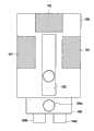
图1是在一个实施例下的衬底加工系统(SPS)。 Figure 1 is a substrate processing system (SPS) under one embodiment. the
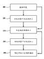
图2是在一个实施例下的用于组合工艺序列集成的流程图。 Figure 2 is a flow diagram for combinatorial process sequence integration, under one embodiment. the
图3是在一个实施例下的包括位隔离加工和/或传统加工的组合工艺序列集成工艺流程。 Figure 3 is a combined process sequence integrated process flow including bit isolation processing and/or conventional processing, under one embodiment. the
图4是在一个实施例下的集成加工工具的框图,该集成加工工具在此称为多通道位隔离反应器(MCSIR)。 Figure 4 is a block diagram of an integrated processing tool, referred to herein as a Multi-Channel Site Isolation Reactor (MCSIR), under one embodiment. the
图5是在一个实施例下的MCSIR的位隔离加工模块(SIPM)。 Figure 5 is a bit isolation processing module (SIPM) of MCSIR under one embodiment. the
图6示出在一个实施例下的在SIPM的一个子集的构件之间的连接。 Figure 6 shows connections between components in a subset of SIPM, under one embodiment. the
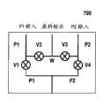
图7是在一个实施例下的包括独立过程和废料路径的流动池的框图。 Figure 7 is a block diagram of a flow cell including separate process and waste paths, under one embodiment. the
图8示出在一个实施例下的包括与卡盘配合的流动池组件的MCSIR。 Figure 8 shows an MCSIR including a flow cell assembly mated with a chuck, under one embodiment. the
图9示出了一个实施例的液力密封系统。 Figure 9 shows a hydraulic sealing system of one embodiment. the
具体实施方式Detailed ways
下文描述的是一种集成加工工具,在此称为多通道位隔离反应器(MCSIR)。所述MCSIR由整片加工模块和组合的位隔离(site-isolated)加工模块构成。集成加工工具的主要用途在于,实现在全衬底和全衬底的多个位隔离区域之间的混合模式加工。同样地,从公共传送系统馈送(feed)用于加工模块中的化学制品,该公共传送系统包括一组第一歧管,所述第一歧管能够产生多种溶液,采用组合方式可改变所述溶液的成分并且所述溶液的组分可被指定为用于工艺步骤的配方的一部分。为了允许彻底的溶液混合以及精确的温度和PH值控制,每个第一歧管的输出连接到至少一个混合导管。每个混合导管的输出接着分配到一组第二歧管中的一个或多个。每组第二歧管的输出馈送加工模块的一个或多个反应器。除了提供在混合导管中静态混合的溶液之外,第二组歧管还能够同时分配多种化学制品,以易于对溶液进行动态协调混合。 Described below is an integrated processing tool, referred to herein as a Multi-Channel Site Isolation Reactor (MCSIR). The MCSIR consists of monolithic processing modules and combined site-isolated processing modules. The main use of integrated processing tools is to enable mixed-mode processing between full substrates and multiple bit-isolated regions of full substrates. Likewise, the chemicals used in the processing modules are fed from a common delivery system comprising a set of first manifolds capable of producing a variety of solutions, the combinations of which can be varied. The components of the solution and the components of the solution may be specified as part of the recipe for the process steps. To allow thorough solution mixing and precise temperature and pH control, the output of each first manifold is connected to at least one mixing conduit. The output of each mixing conduit is then distributed to one or more of a set of second manifolds. The output of each set of second manifolds feeds one or more reactors of the processing module. In addition to providing solutions that are statically mixed in the mixing conduits, the second set of manifolds is capable of dispensing multiple chemicals simultaneously for easy dynamic coordinated mixing of the solutions. the
对于位隔离加工,MCSIR集成多个独立受控的工艺室,它们共同处于在全衬底上的多个独立位置处。MCSIR提供如下能力,即,以一种或多种串行和/或并行方式将多种化学溶液或成分混合并分配到衬底上,并提供如下能力,即,针对任意数量的反应器或反应器的一个或多个子集独立改变流量和/或溶液成分。MCSIR提供如下能力,即,同步加工步骤,并且当用于工艺步骤的全局参数要求针对非位隔离控制参数(例如,晶片衬底的温度、反应器高度/体积等等)进行这种同步时,控制遍历所有位隔离反应器的严格定时。 For bit-isolated processing, MCSIR integrates multiple independently controlled process chambers that are co-located at multiple independent locations on the full substrate. MCSIR provides the ability to mix and distribute multiple chemical solutions or components onto a substrate in one or more serial and/or parallel fashions and to provide the ability to target any number of reactors or reactions One or more subsets of the detectors independently vary flow and/or solution composition. MCSIR provides the ability to synchronize process steps, and when global parameters for process steps require such synchronization for non-bit-isolated control parameters (e.g., temperature of wafer substrate, reactor height/volume, etc.), Controls tight timing of traversal of all bit isolation reactors. the
通过遍历单一的200或300毫米硅衬底提供多个单独受控并且垂直的反应器或工艺室,在此所述的MCSIR解决如下问题,即,致使传统的半导体制造设备并不良好地适于材料开发和集成。每个位隔离反应器的构造和流体动力性质典型地与生产堆成比例,从而易于对整片进行成比例增大,而又使工艺集成步骤变化甚微。另外,MCSIR的材料传送系统被 配置为,使被提供给所述室的材料的数量以及用于实现材料集成的工艺序列的各步骤均具有较大的灵活性。相比于生产工具,反应器小型化以及用于材料研究和集成的宽松的设备要求也降低了设备的成本。 By providing multiple individually controlled and vertical reactors or process chambers across a single 200 or 300 mm silicon substrate, the MCSIR described herein addresses problems that render conventional semiconductor fabrication equipment not well suited for Materials development and integration. The configuration and hydrodynamic properties of each bit-isolated reactor are typically scaled to the production stack, allowing easy scale-up of the entire stack with little variation in process integration steps. In addition, MCSIR's material delivery system is configured to allow greater flexibility in the amount of material provided to the chamber as well as in the steps of the process sequence used to achieve material integration. Reactor miniaturization and relaxed equipment requirements for materials research and integration also reduce the cost of equipment compared to production tools. the
下文描述的是用于加工衬底的系统和方法(例如,在衬底上形成材料)。用于加工衬底的系统和方法,统称为“衬底加工系统”(SPS),包括组合加工、与传统衬底加工集成的组合工艺序列、和/或位隔离加工,如下文详述。举例而言,一个实施例的SPS能够以非常低的成本在衬底上产生非常小的结构和特征部(例如,纳米尺寸量级),这些结构和特征部可以用于诸如电子构件和平板显示器的多种产品的商业制造。下文所述的各种不同的系统和方法仅仅作为实例展现,而并不意在将在此所述和要求保护的系统和方法限制于组合加工、与传统衬底加工集成的组合工艺序列、和/或位隔离加工的特定组合。进一步,下文所述的系统和方法并不限于特定工艺(例如,湿法加工、干法加工等等)。 Described below are systems and methods for processing substrates (eg, forming materials on substrates). Systems and methods for processing substrates, collectively referred to as "substrate processing systems" (SPS), include combined processing, combined process sequences integrated with conventional substrate processing, and/or bit-segregated processing, as detailed below. For example, the SPS of one embodiment can produce very small structures and features (e.g., on the nanometer scale) on substrates at very low cost, which can be used in applications such as electronic components and flat panel displays. commercial manufacture of a wide variety of products. The various systems and methods described below are presented as examples only, and are not intended to limit the systems and methods described and claimed herein to combinatorial processing, combinatorial process sequences integrated with conventional substrate processing, and/or or a specific combination of bit-isolation processing. Further, the systems and methods described below are not limited to a particular process (eg, wet processing, dry processing, etc.). the
在接下来的描述中,引入多个具体细节来提供对SPS的各实施例的透彻理解并能够描述SPS的各实施例。然而,本领域技术人员将认识到,没有所述具体细节中的一个或多个,或者采用其它构件、系统等等,也可以实施这些实施例。在其它情况中,为避免使所公开的实施例的各方面变得不清晰,并不显示或详细描述众所周知的结构或操作。 In the ensuing description, numerous specific details are introduced to provide a thorough understanding of and enable description of various embodiments of the SPS. However, one skilled in the art will recognize that the embodiments may be practiced without one or more of the specific details, or with other components, systems, etc. In other instances, well-known structures or operations are not shown or described in detail to avoid obscuring aspects of the disclosed embodiments. the
一个实施例的SPS主要包括设计用于承接至少一个衬底的至少一个接口。所述SPS还包括多个连接到上述接口的模块。上述模块,在此也称为构件,包括预加工模块、加工模块、后加工模块,但可以包括任意数量和/或类型的其它模块,其中任意模块可包括所述预加工、加工、和/或后加工模块的功能。所述SPS不要求包括任意特定模块类型中的每一种的至少一个。另外,所有预加工、加工、后加工模块的功能可嵌入单一模块中。所述多个模块中的每个模块可根据在至少一个其它模块中所含工艺的需要包含多种加工中的至少一种。所述SPS还包括至少一个手柄,其连接到所述接口并被配置为使衬底在接口和一个或多个模块之间移动。 The SPS of an embodiment essentially comprises at least one interface designed to receive at least one substrate. The SPS also includes a plurality of modules connected to the aforementioned interface. The aforementioned modules, also referred to herein as components, include preprocessing modules, processing modules, postprocessing modules, but may include any number and/or type of other modules, wherein any module may include the preprocessing, processing, and/or Functions of the post-processing module. The SPS is not required to include at least one of each of any particular module types. In addition, the functions of all pre-processing, processing and post-processing modules can be embedded in a single module. Each module of the plurality of modules may contain at least one of a variety of processes as required by the processes contained in at least one other module. The SPS also includes at least one handle connected to the interface and configured to move a substrate between the interface and the one or more modules. the
图1是在一个实施例下的衬底加工系统(SPS)100。衬底加工系统 100包括预加工模块101、加工模块102、和后加工模块103。SPS 100不要求包括加工模块类型中的每一种的至少一个;例如,特定工艺流程可仅仅包括加工模块102和用于将衬底移入和移出系统100的装置。另外,所有预加工、加工和后加工模块的功能可嵌入在单一模块中。模块101、102、103每一个均可根据模块101、102、103将要用于的衬底加工的类型的需要使用适当的装置(特别地,传统的商业衬底加工装置)来执行。模块101、102、103可以根据衬底和/或工艺的具体特性而改造和/或添加地执行。 Figure 1 is a substrate processing system (SPS) 100 under one embodiment. The
衬底通过系统接口104-也称为工厂接口104-进入和离开系统100。可以在系统100中一次加工单个衬底,或者可以成批地一次加工多个衬底。系统接口104包括衬底手柄104a(其可例如使用自动装置执行),其将衬底移入和移出系统100。为了便于将衬底移入和移出系统100,系统接口104包括衬底装载站104b和衬底卸载站104c(也各自称为前开式晶圆盒(FOUP)装载站104b和FOUP卸载站104c)。 Substrates enter and exit the
在已经得到加工的衬底通过衬底手柄104a从系统100移出并放置在衬底卸载站104c上(以便最终移动到另一位置)之后,已经预先放置在衬底装载站104b上的新衬底通过衬底手柄104a从衬底装载站104b取出,并移动到系统100中以便进行加工。可以使用在加工衬底领域的技术人员公知的传统装置和方法来实现系统接口104(包括衬底手柄104a、衬底装载站104b、衬底卸载站104c)。一个或多个替换性实施例的系统100可包括多个系统接口,每个系统接口可如上所述进行构造和操作。 After a substrate that has been processed is removed from the
一旦处于系统100中,衬底操作系统105就可用于将由系统100所加工的衬底在系统100的不同模块101-103之间移动。类似于系统接口104的衬底手柄104a,衬底操作系统105可以例如使用一个或多个自动装置来执行。如果模块101、102、103既包括湿法加工模块也包括干法加工模块,则衬底操作系统105包括至少两种装置:干法衬底手柄,其用于将衬底移入和移出干法加工模块和系统接口104以及移出干化模块;和湿法衬底手柄,其用于将衬底移入和移出湿法加工模块以及移入干化模块。衬底操作系统105可使用在加工衬底的领域中的技术人员公知的 装置和方法来执行。 Once in the
在衬底正在通过系统接口104移入或移出系统100之外的其它时刻,系统100与外界环境密封隔离。根据由系统100将要执行的加工,在系统100内处于预加工模块101、加工模块102、后加工模块103之外的环境(为方便起见,有时在下文中称为“系统环境”)可保持处于大气压、保持处于真空压力、和/或被加压(即,保持处于比大气压更高的压力下)。类似地,系统环境可保持处于系统100之外的环境的外界温度,或者处于比该外界温度更高或更低的温度下。 At other times when substrates are being moved into or out of the
进一步,根据期望可以控制系统环境的气体成分。例如,系统环境可为外界空气(典型地,被控制以降低来自外部环境的污染)。系统环境也可被控制而整体地或局部地包括一种或多种指定气体,例如,在用于加工半导体晶片的系统中,系统环境可被控制为氮气或惰性气体。系统环境也可以被控制以排除一种或多种指定气体,例如,氧气可以从系统环境中排除,以降低在系统中所加工的衬底(或其上形成的材料)的氧化的发生率。 Further, the gaseous composition of the system environment can be controlled as desired. For example, the system environment may be outside air (typically controlled to reduce contamination from the external environment). The system environment may also be controlled to include one or more specified gases, either wholly or locally, for example, in a system for processing semiconductor wafers, the system environment may be controlled to be nitrogen or an inert gas. The system environment can also be controlled to exclude one or more specified gases, for example, oxygen can be excluded from the system environment to reduce the incidence of oxidation of substrates (or materials formed thereon) processed in the system. the
替换性实施例的SPS可包括用于加工单一晶片或单组晶片的每种类型的模块中的多个;因此,多种形式的SPS可以作为单一系统并行操作。这就能够改进由SPS所加工的衬底的产量。这还能够增加冗余,这样,即使在系统的一个或多个模块呈现为一个时段内不可操作(例如,为了进行预防性维护、修理等等)时,也可以保持系统可行性。 The SPS of an alternative embodiment may include multiples of each type of module for processing a single wafer or group of wafers; thus, multiple forms of SPS may operate in parallel as a single system. This can improve the yield of substrates processed by SPS. This can also add redundancy so that system viability can be maintained even if one or more modules of the system are rendered inoperable for a period of time (eg, for preventive maintenance, repair, etc.). the
上文所述的SPS以示例性展示,并且可以使用包含其它数量的加工模块的系统。进一步,可以使用除上文所述模块之外类型的加工模块。在一些加工系统中,可以替代用于将衬底移入和移出系统的衬底手柄,而采取对衬底进行手动装载和卸载。 The SPS described above is shown by way of example, and systems containing other numbers of process modules may be used. Further, processing modules of types other than those described above may be used. In some processing systems, manual loading and unloading of substrates may be employed instead of a substrate handle for moving substrates into and out of the system. the
上文所述的SPS 100可包括用于对单一衬底上的各区域进行组合加工的一个或多个模块(也称为构件)和/或方法。通常,通过将加工材料传送到衬底上的一个或多个区域和/或对区域进行改造,来组合加工区域阵列。一个实施例的衬底上的区域包括但不限于预定的区域以及在衬底加工期间和/或作为衬底加工的结果而确定的区域。 The
图2是在一个实施例下的用于组合工艺序列集成的流程图。该实施例可采用将执行所期望的分析过程的加工工具(其可以是也可以不是由集体执行有效单元加工的分立单元模块构成的集成工具)。在一个实施例中,加工工具可在单一的整体式衬底中所含的单独区域内以离散方式执行上述过程,比如IC加工中所使用的直径300mm的晶片。衬底被设置于系统200,并且以离散且优选分离的方式(以串行、并行或者串行-并行模式)被加工,从而使衬底的至少两个区域得到彼此不同的加工210。以组合方式加工的衬底可以可选地提前220和/或随后230采用至少一个过程或过程步骤以传统方式得到加工,从而使整个或大致接近整个衬底承受相同的加工条件。这就允许,在构建终端设备、集成电路等等所需要的工艺流程的期望节段中使用所述组合加工/组合工艺序列集成途径。 Figure 2 is a flow diagram for combinatorial process sequence integration, under one embodiment. This embodiment may employ a processing tool (which may or may not be an integrated tool consisting of discrete unit modules that collectively perform efficient unit processing) that will perform the desired analysis process. In one embodiment, a processing tool may perform the above processes in a discrete manner within individual regions contained within a single monolithic substrate, such as a 300 mm diameter wafer used in IC processing. A substrate is provided in the
可以使用传统的分析方法针对感兴趣的属性来测试240被加工区域,诸如所产生的器件或器件的各部分,所述测试240例如为针对诸如产量的属性通过电阻、线路电阻、电容等进行的参数测试,和/或针对诸如应力迁移、电迁移、偏置热应力、时变介质击穿的属性所进行的可靠性测试,以及本领域技术人员所公知的相关测试。被加工区域可被同时测试、顺次测试、或者以并行-串行模式测试,在并行-串行模式中,第一多个区域被同时测试,接着第二多个区域被同时测试。测试240可选地在用于组合工艺序列集成的方法的一个或多个替换性实施例中被执行。 The processed area, such as the resulting device or portions of a device, can be tested 240 for properties of interest using conventional analytical methods, for example by resistance, line resistance, capacitance, etc., for properties such as yield Parametric tests, and/or reliability tests for properties such as stress migration, electromigration, bias thermal stress, time-varying dielectric breakdown, and related tests known to those skilled in the art. The processed areas may be tested simultaneously, sequentially, or in a parallel-serial mode in which a first plurality of areas are tested simultaneously, followed by a second plurality of areas. Testing 240 is optionally performed in one or more alternative embodiments of the method for combinatorial process sequence integration. the
一个实施例的组合工艺序列集成使用执行一个或多个过程的加工工具,在此称为位隔离加工工具(也称为位隔离反应器(SIR))。在一个实施例中,位隔离加工工具以离散隔离方式(以串行、并行或者串行-并行模式)在衬底的单独区域内加工衬底(例如,衬底的至少两个区域被彼此不同地加工)。在加工区域阵列的过程中,如在此所述,加工材料可被传送到衬底上的各区域(包括预定区域),和/或各区域(包括预定区域)可使用任意数量的位隔离加工过程或序列组合以任意数量的传统加工过程或序列而被改造。 The combined process sequence of one embodiment integrates the use of a process tool, referred to herein as a site-isolated process tool (also referred to as a site-isolated reactor (SIR)), that performs one or more processes. In one embodiment, the bit-isolated processing tool processes the substrate in separate regions of the substrate (e.g., at least two regions of the substrate are differentiated from each other) in a discretely isolated manner (in serial, parallel, or serial-parallel mode). ground processing). In processing an array of regions, as described herein, process material may be delivered to regions (including predetermined regions) on the substrate, and/or regions (including predetermined regions) may be processed using any number of bit-isolated A process or sequence combination is adapted in any number of traditional processes or sequences. the
例如,在此处描述的组合工艺序列集成的方法接收来自从包含沉积、图案化、蚀刻、清洗、平面化、植入和处理的组所选出的至少一个第一 过程的衬底。上述方法通过与衬底的至少一个其它区域不同地加工衬底的至少一个区域,产生经加工的衬底。所述加工包括改造至少一个区域,其中,改造包括物理改造、化学改造、电改造、热改造、磁改造、光子改造和光解改造中的至少一种。所述加工形成在衬底上的被不同加工的区域的至少一个阵列。在一个实施例中,上述加工包括使用材料、加工条件、工艺序列、工艺序列集成、工艺序列条件中的至少一种进行改造。在一个其它实施例中,上述经加工的衬底承受选自包括沉积、图案化、蚀刻、清洗、平面化、植入和处理的组的至少一个额外的过程。 For example, the method of combined process sequence integration described herein receives a substrate from at least one first process selected from the group consisting of deposition, patterning, etching, cleaning, planarization, implantation, and processing. The above method produces a processed substrate by processing at least one region of the substrate differently than at least one other region of the substrate. The processing includes modifying at least one region, wherein modifying includes at least one of physical modification, chemical modification, electrical modification, thermal modification, magnetic modification, photonic modification, and photolytic modification. The processing forms at least one array of differently processed regions on the substrate. In one embodiment, the above-mentioned processing includes using at least one of materials, processing conditions, process sequences, process sequence integration, and process sequence conditions for modification. In one other embodiment, the above-mentioned processed substrate is subjected to at least one additional process selected from the group consisting of deposition, patterning, etching, cleaning, planarization, implantation and treatment. the
作为另一示例,在此处所述的组合工艺序列集成的方法通过不同于衬底的至少一个其它区域而对衬底的至少一个区域进行加工,产生经加工的衬底。所述加工包括改造至少一个区域,其中改造包括物理改造、化学改造、电改造、热改造、磁改造、光子改造和光解改造中的至少一种。所述加工形成在衬底上被不同加工的区域的至少一个阵列。所述方法通过将被加工衬底提供给选自包括沉积、图案化、蚀刻、清洗、平面化、植入和处理的组的至少一个额外过程而得以继续。在一个实施例中,上述加工包括使用材料、加工条件、工艺序列、工艺序列集成、工艺序列条件中的至少一种进行改造。 As another example, methods of combined process sequence integration described herein produce a processed substrate by processing at least one region of a substrate differently than at least one other region of the substrate. The processing includes modifying at least one region, wherein modifying includes at least one of physical modification, chemical modification, electrical modification, thermal modification, magnetic modification, photonic modification, and photolytic modification. The processing forms at least one array of differently processed regions on the substrate. The method continues by subjecting the processed substrate to at least one additional process selected from the group consisting of deposition, patterning, etching, cleaning, planarization, implantation and treatment. In one embodiment, the above-mentioned processing includes using at least one of materials, processing conditions, process sequences, process sequence integration, and process sequence conditions for modification. the
图3是在一个实施例下的组合工艺序列集成工艺流程300,其包括位隔离加工和/或传统加工。在此处的各实施例下的加工序列的一个示例如下:使用传统过程N加工衬底,然后使用位隔离过程N+1加工衬底,然后使用位隔离过程N+2加工衬底,然后使用传统过程N+3加工衬底,然后执行E测试(例如电测试)。在此处的实施例下的加工序列的另一示例如下:使用位隔离过程N加工衬底,然后使用位隔离过程N+1加工衬底,然后使用传统过程N+2加工衬底,然后使用位隔离过程N+3加工衬底,然后执行E测试。在此处的实施例下的加工序列的又一示例如下:使用位隔离过程N加工衬底,然后使用传统过程N+1加工衬底,然后使用位隔离过程N+2加工衬底,然后使用传统过程N+3加工衬底,然后执行E测试。根据工艺流程300可以实现各种其它加工序列。 FIG. 3 is a combined process sequence integrated process flow 300 that includes bit isolation processing and/or conventional processing, under one embodiment. One example of a processing sequence under the various embodiments herein is as follows: process the substrate using conventional process N, then process the substrate using bit isolation process N+1, then process the substrate using bit isolation process N+2, then process the substrate using Conventional process N+3 processes the substrate and then performs E-test (eg electrical test). Another example of a processing sequence under the embodiments herein is as follows: process substrate using bit isolation process N, then process substrate using bit isolation process N+1, then process substrate using conventional process N+2, then process substrate using The bit isolation process N+3 processes the substrate and then performs the E test. Yet another example of a processing sequence under the embodiments herein is as follows: process substrate using bit isolation process N, then process substrate using conventional process N+1, then process substrate using bit isolation process N+2, then process substrate using The traditional process N+3 processes the substrate and then performs the E-test. Various other processing sequences may be implemented according to process flow 300 . the
组合工艺序列集成因此例如产生包含模具阵列的半导体晶片302,模 具阵列包括能够作为包含预期集成电路的测试模具和/或实体产品模具的多个模具304。使用上述组合工艺序列集成方法,可以加工和/或产生无图形晶片、有图形晶片、器件、功能芯片、功能器件、测试结构、半导体、集成电路、平板显示器、光电器件、数据存储器件、电磁器件、磁光器件、分子电子器件、太阳能电池、光子器件、成套器件。组合工艺序列集成可用于整个工艺流程的任意期望的节段和/或部分。可以在工艺流程之内的每个加工步骤和/或加工步骤系列之后根据需要和/或期望执行包括电测试的特征评定。 Combinatorial process sequence integration thus produces, for example, a semiconductor wafer 302 comprising an array of dies including a plurality of dies 304 that can serve as test dies and/or physical product dies containing desired integrated circuits. Unpatterned wafers, patterned wafers, devices, functional chips, functional devices, test structures, semiconductors, integrated circuits, flat panel displays, optoelectronic devices, data storage devices, electromagnetic devices can be processed and/or produced using the above combined process sequence integration method , Magneto-optical devices, molecular electronic devices, solar cells, photonic devices, complete sets of devices. Combined process sequence integration can be used for any desired segment and/or part of the overall process flow. Characterization, including electrical testing, may be performed as needed and/or desired after each processing step and/or series of processing steps within the process flow. the
SPS的实施例将加工材料传送到在衬底上的一个或多个预定区域,并使用多种不同技术对所传送的材料进行反应。例如,可以使用基于溶液的合成技术、光化学技术、聚合技术、模板法合成技术、外延生长技术,通过溶胶-凝胶转变(Sol-gel)过程、通过热学、红外或微波加热,通过煅烧、烧结或退火,通过热液方法,通过熔剂方法,通过经由溶剂蒸发进行结晶等等,对加工材料进行反应。可用于对感兴趣的加工材料进行反应的其它有用的反应技术对于本领域技术人员显而易见。 Embodiments of SPS deliver process material to one or more predetermined areas on a substrate and react to the delivered material using a variety of different techniques. For example, solution-based synthesis techniques, photochemical techniques, polymerization techniques, template-based synthesis techniques, epitaxial growth techniques, by sol-gel transition (Sol-gel) processes, by thermal, infrared or microwave heating, by calcination, sintering Or annealing, reacting the processed material by the hydrothermal method, by the flux method, by crystallization via solvent evaporation, etc. Other useful reaction techniques that can be used to react the process material of interest will be apparent to those skilled in the art. the
由于衬底的各区域彼此独立地被加工,所以在不同区域处的加工条件可以独立受控。例如,工艺材料量、反应溶剂、加工温度、加工时刻、加工压力、反应终止(quench)的速率、工艺材料的沉积次序、工艺序列步骤等等,可以随衬底上区域变化而不同。因此,例如,当探究材料时,被传送到第一和第二区域的加工材料可以相同也可以不同。如果被传送到第一区域的加工材料与被传送到第二区域的加工材料相同,则这种加工材料可以以或者相同或者不同的浓度提供给衬底上的第一和第二区域。对于将额外的加工材料传送到第一和第二区域等等,这也是可行的。正如传送到第一和第二区域的加工材料,传送到第一和第二区域的额外加工材料可以相同也可以不同,如果相同,则可以以或者相同或者不同的浓度提供给衬底上的第一和第二区域。 Since regions of the substrate are processed independently of each other, the processing conditions at the different regions can be independently controlled. For example, the amount of process material, reaction solvent, process temperature, process time, process pressure, reaction quench rate, process material deposition order, process sequence steps, etc., may vary with the area on the substrate. Thus, for example, when exploring materials, the process material delivered to the first and second regions may or may not be the same. If the processing material delivered to the first region is the same as the processing material delivered to the second region, such processing material may be provided to the first and second regions on the substrate at either the same or different concentrations. This is also possible for conveying additional process material to the first and second regions and so on. As with the process material delivered to the first and second regions, the additional process material delivered to the first and second regions may be the same or different, and if the same, may be provided to the first substrate on the substrate at either the same or different concentrations. One and two regions. the
而且,在衬底上的预定区域内,加工材料可以以均匀或渐变的方式传送。如果相同的加工材料以完全相同的浓度传送到衬底的第一和第二区域,则区域加工所处于的条件(例如反应温度、反应时间等等)可以 随区域的不同而改变。可以被改变的参数包括,例如,材料量、溶剂、工艺温度、工艺时间、执行过程所处于的压力、过程进行所处于的气体环境、淬冷过程所处于的速率、沉积材料的次序等等。其它可以改变的过程参数对于本领域技术人员可以显而易见。 Furthermore, the processing material can be delivered in a uniform or gradual manner within a predetermined area on the substrate. If the same process material is delivered to the first and second regions of the substrate at exactly the same concentration, the conditions under which the regions are processed (e.g., reaction temperature, reaction time, etc.) may vary from region to region. Parameters that may be varied include, for example, material amounts, solvents, process temperature, process time, pressure at which the process is performed, gas environment at which the process is performed, rate at which the quench process is performed, the order in which materials are deposited, and the like. Other process parameters that may be varied will be apparent to those skilled in the art. the
而且,一实施例通过将基本相同的加工材料以基本一致的浓度传送到在具有不同表面(例如介电材料表面和导电表面)的第一和第二衬底上的对应区域,以便在IC芯片上显现不同的区域部分,并随后使衬底上的工艺材料承受第一组工艺条件,而形成至少两个不同的材料阵列。使用这种方法,可以研究并接着优化过程参数或材料对不同衬底表面的影响。 Furthermore, an embodiment provides a process material on an IC chip by delivering substantially the same processing material at a substantially uniform concentration to corresponding regions on first and second substrates having different surfaces (e.g., a dielectric material surface and a conductive surface). The different region portions are developed on the substrate, and then the process material on the substrate is subjected to a first set of process conditions to form at least two different arrays of materials. Using this approach, the influence of process parameters or materials on different substrate surfaces can be studied and then optimized. the
在单独区域加工中采用的加工材料必须经常被防止移动到相邻区域。更简单地,这可以通过如下过程来确保,即,在衬底上的区域之间留下足量的空间,从而使不同的加工材料不能在区域间互相扩散。而且,这可以通过如下过程确保,即,在加工期间在衬底上的不同区域之间提供合适的屏障。在一种途径中,机械器件或物理结构限定衬底上的不同区域。例如,可以使用壁或其它物理屏障来防止在单独区域中的材料移动到相邻区域。在完成合成之后,可以去除这种壁或物理屏障。本领域技术人员将认知,有时在掩蔽材料阵列之前去除壁或物理屏障可能是有益的。 Machining material employed in machining of a single area must often be prevented from moving to adjacent areas. More simply, this can be ensured by leaving a sufficient amount of space between regions on the substrate so that different process materials cannot interdiffuse between the regions. Furthermore, this can be ensured by providing suitable barriers between different regions on the substrate during processing. In one approach, mechanical devices or physical structures define different regions on the substrate. For example, walls or other physical barriers may be used to prevent material in a single area from moving to an adjacent area. After the synthesis is complete, such walls or physical barriers can be removed. Those skilled in the art will recognize that it may sometimes be beneficial to remove walls or physical barriers prior to masking the array of materials. the
在其它实施例中,在不需要物理接触衬底的屏障的情况下,可以实现上述加工。例如,当改造面积在尺寸上略小于和/或等于衬底上的感兴趣的离散区域时,可以使用激光器、辐射灯、UV辐射源、其它“点”源来以位置可寻址的方式加工区域。在又一实施例中,物理屏障可用于将所述加工根本上掩蔽和/或限制于其中物理屏障并不物理接触衬底的期望区域和/或区域部分。例如,物理屏障可用于将加工根本上阻挡和/或抑制于特定区域和/或区域部分。例如,诸如掩膜或遮板的屏幕可用于阻挡诸如来自PVD(即,溅射)或蒸气源的蒸汽通量。不透明与透明相间的掩膜可用于让特定的辐射通过透明区域,以实现在衬底上指定区域中的加工。在又一实施例中,优选诸如氩气(Ar)的惰性气体的气流,可用 于筛出气态反应剂,和/或限制这种反应剂的浓度,从而将这种反应剂的效果从特定区域有效地筛出。采用这种方式,衬底上的指定区域可以得到不同加工,而不必将物理屏障与衬底相关联。这种途径尤其适于基于顺次气相真空的表面动力过程,例如原子层沉积及其变化形式(例如,引入/增强了离子、原子团、和等离子体)。 In other embodiments, the processing described above can be accomplished without the need for a barrier that physically contacts the substrate. For example, lasers, radiant lamps, UV radiation sources, other "point" sources can be used to process in a position-addressable manner when the modified area is slightly smaller and/or equal in size to the discrete area of interest on the substrate. area. In yet another embodiment, a physical barrier may be used to substantially mask and/or confine the processing to desired regions and/or portions of regions where the physical barrier does not physically contact the substrate. For example, physical barriers can be used to substantially block and/or inhibit processing to specific regions and/or portions of regions. For example, a screen such as a mask or shutter can be used to block the flux of vapor such as from a PVD (ie, sputtering) or vapor source. Alternating opaque and transparent masks can be used to pass specific radiation through transparent areas to enable processing in designated areas on the substrate. In yet another embodiment, a flow of an inert gas, preferably such as argon (Ar), may be used to screen out gaseous reactants, and/or limit the concentration of such reactants, thereby limiting the effects of such reactants from specific areas. Effectively sift out. In this way, designated regions on the substrate can be processed differently without associating physical barriers with the substrate. This approach is particularly suitable for sequential gas-phase vacuum-based surface kinetic processes, such as atomic layer deposition and its variants (eg, introduced/enhanced ions, radicals, and plasmas). the
一个实施例的SPS包括如下加工工具,其被配置为实现遍历整个衬底的均匀加工以及单独的对衬底的一个或多个离散区域的独立加工。在此描述的加工工具,包括在上文参照图2和3所述的组合工艺序列集成工艺流程下的操作,可以是类似上文所述的SPS 100的衬底加工系统的构件和/或上文参照图1所述的SPS 100的一个或多个模块。例如,图3的组合工艺序列集成工艺流程300可以在SPS 100(图1)的加工模块102中实施。类似地,作为另一示例,组合工艺序列集成工艺流程300可以遍历SPS 100(图1)的一个或多个加工模块101、102、103得到实施。 The SPS of one embodiment includes a processing tool configured to achieve uniform processing across an entire substrate as well as separate independent processing of one or more discrete regions of the substrate. The processing tools described herein, including operations under the combined process sequence integrated process flow described above with reference to FIGS. One or more modules of the
一个实施例的SPS包括支持整片加工和组合加工的集成加工工具。图4是在一个实施例下的集成加工工具400的框图,集成加工工具400在此称为多通道位隔离反应器(MCSIR)400。MCSIR 400包括整片加工模块405和位隔离加工模块(SIPM)409,如下文所详述。MCSIR 400结合一种大容量化学制品分配系统,以提供实现工艺序列所必要的化工原料401,还结合形式为混合导管和分配歧管的化学混合和定序硬件,以提供动态混合任意成分的化学溶液的能力,并且对通过反应器的化学制品以任意次序进行定序达任意持续时间。MCSIR 400使用计算机化硬件控制器402进行控制,并且一个实施例的同一控制器实现在整片反应器和位隔离反应器中的加工。晶片使用工厂接口404定序通过MCSIR 400。整片和位隔离反应器在所有控制方面可比。MCSIR 400的每个反应器或通道被配置为,允许植入复杂的湿法/蒸气工艺序列,如在此所述。 The SPS of one embodiment includes integrated processing tools that support full wafer processing and combination processing. FIG. 4 is a block diagram of an
通常,整片加工模块405包括连接到整片反应器的工艺歧管。工艺歧管连接到化学制品401,并被配置为将化学制品401馈送或传送到整片反应器。整片反应器被配置为,使用所传送的化学制品实现遍历整个晶片或衬底表面(例如,8英寸晶片、12英寸晶片等等)的均匀加工。 Typically,
形成对照的是,SIPM 409是位隔离加工器,其能够使用多通道或工艺路径来单独加工遍历晶片的多个离散区域(例如,28个区域)。为了使该示例清晰起见,SIMP 409的这一示例显示正在被两个工艺路径或通道中的任一个馈送的单一位隔离反应器,但是MCSIR可包括任意数量的位隔离反应器以及连接到每个反应器的任意数量的工艺路径。 In contrast, the
SIPM 409使用通常包括一套或一组第一歧管(例如,混合导管(MV)1歧管)的传送系统馈送或分配化学制品401。每个第一歧管的输出连接到混合导管(例如,混合导管1等等)。混合导管歧管允许以任意速率针对每个混合导管对大块化学制品进行混合,然后混合导管充当混合的化学制品溶液的临时存储装置。
每个混合导管的输出馈送一组第二歧管中的一个或多个(例如,工艺通道1位歧管、工艺通道2位歧管)。每组第二歧管的输出馈送位隔离反应器。所述一组第二歧管通常允许通过在一组流动池中的两个工艺路径中的任一个(例如,通道1、通道2)对混合导管溶液和/或大块化学制品进行定序。流动池包括位隔离反应器的顶表面,并且反应器套管包括反应器的侧壁。被加工的衬底包括反应器的底部。每个位隔离反应器实现衬底的专门区域的单独加工,如在此所述。 The output of each mixing conduit feeds one or more of a set of second manifolds (eg,
MCSIR 400的示例并不包括在用于整片反应器的工艺路径中的混合导管。然而,可能并且有时期望的是,在整片反应器工艺路径中包含混合导管,以便以类似于SIPM的方式构建整片加工模块。 The
图5是在一个实施例下的MCSIR的SIPM 500。SIPM 500通过同时控制在多个并行反应器中的反应,来管理或控制衬底的不同区域的同时加工。每个反应器就位而靠近衬底的特定区域(例如,晶片)。举例而言,反应器控制包括控制反应剂流动、反应剂混合、反应剂传送、反应剂和/或反应器温度、和/或反应剂pH值等等。 Figure 5 is a
SIPM 500包括连接到第一混合组件514的第一分配组件512。第一分配组件512包括数量为N的混合导管歧管5121-512N,其中混合导管歧管的数目N可为任意数量。一个实施例的第一分配组件512包括二十八(28)个混合导管歧管,但是SPS并不限于这种数量的混合导管歧管, 并且可以包括任意数量的混合导管歧管。每个混合导管歧管的输入连接到一个或多个化学制品501。作为示例,一个实施例的混合导管歧管包括八(8)个输入,并且每个输入连接到一个不同的化学制品501。然而,混合导管歧管并不限于八(8)个输入,并且每个输入不限于连接与任意其它歧管输入不同的组分。另外,分配组件512的所有混合导管歧管并不限于呈现相同配置。进一步,其它构件(例如,阀、调节器、泵等等)可协调连接在组分和混合导管歧管之间。
第一混合组件514包括数量为N的混合导管5141-514N,其中混合导管的数目N可为任意数量。一个实施例的第一混合组件514包括二十八(28)个混合导管,但SPS并不限于这一数量的混合导管,并且可以包括任意数量的混合导管。每个混合导管的输入连接到第一分配组件512的混合导管歧管的输出。作为示例,一个实施例的混合导管包括一(1)个输入,其连接到第一分配组件512的混合导管歧管的输出。作为更为具体的示例,第一混合导管5141的输入连接到第一混合导管歧管5121的输出。然而,混合导管并不限于一(1)个输入,并且每个输入并不限于向第一分配组件512的一个混合导管歧管的连接。 The first mixing assembly 514 includes a number N of mixing conduits 5141-514N, where the number N of mixing conduits can be any number. The first mixing assembly 514 of one embodiment includes twenty-eight (28) mixing conduits, although the SPS is not limited to this number of mixing conduits and may include any number of mixing conduits. The input of each mixing conduit is connected to the output of the mixing conduit manifold of the
SIPM 500进一步包括连接到第二混合组件524的第二分配组件522。第二分配组件522包括数量为N的混合导管歧管5221-522N,其中混合导管歧管的数目N可为任意数量。一个实施例的第二分配组件522包括二十八(28)个混合导管歧管,但SPS并不限于这一数量的混合导管歧管。每个混合导管歧管的输入连接到一个或多个化学制品501。作为示例,并且如上所述,一个实施例的混合导管歧管包括八(8)个输入,并且每个输入连接到一个不同的化学制品501。然而,混合导管歧管并不限于八(8)个输入,并且每个输入并不限于连接与任意其它歧管输入不同的组分。另外,其它构件(例如,阀、调节器、混合器等等)可以协调连接在组分和混合导管歧管之间。
第二混合组件524包括数量为N的混合导管5241-524N,其中混合导管的数目N可为任意数量。一个实施例的第二混合组件524包括二十八(28)个混合导管,但SPS并不限于这一数量的混合导管。每个混合 导管的输入连接到第一分配组件522的混合导管歧管的输出。作为示例,一个实施例的混合导管包括一(1)个与第一分配组件522的混合导管歧管的输出相连的输入。作为更具体的示例,第一混合导管5241的输入连接到第一混合导管歧管5221的输出。然而,混合导管并不限于一(1)个输入,并且每个输入并不限于向第一分配组件522的一个混合导管歧管的连接。 The second mixing assembly 524 includes a number N of mixing conduits 5241-524N, where the number N of mixing conduits can be any number. The second mixing assembly 524 of one embodiment includes twenty-eight (28) mixing conduits, although the SPS is not limited to this number of mixing conduits. The input of each mixing conduit is connected to the output of the mixing conduit manifold of the first distribution assembly 522. As an example, the mixing conduit of one embodiment includes one (1) input connected to the output of the mixing conduit manifold of the first distribution assembly 522 . As a more specific example, the input of the
SPS被模块化,因此SPS的替换性实施例可包括数量不同的分配组件和/或混合组件。例如,替换性实施例的SPS可包括两个额外的分配组件,而每个额外的分配组件连接到额外的混合组件。作为另一示例,替换性实施例的SPS仅仅包括如上所述的第一分配组件512和第一混合组件514,并且不包括第二分配组件522和第二混合组件524。进一步,替换性实施例的SPS可包括比上文所述数量更小或更大的混合导管歧管和/或混合导管。另外,替换性实施例包括混合导管歧管和/或混合导管的不同配置;例如,两个混合导管歧管可连接到单个混合导管。 The SPS is modular, so alternative embodiments of the SPS may include a different number of dispensing and/or mixing components. For example, the SPS of an alternative embodiment may include two additional distribution assemblies, with each additional distribution assembly connected to an additional mixing assembly. As another example, the SPS of an alternative embodiment includes only the
SIPM 500包括第三分配组件532。第三分配组件532包括数量为N的位歧管5321-532N,其中位歧管的数目N可为任意数量。一个实施例的第三分配组件532包括二十八(28)个位歧管,但是SPS并不限于这一数量的位歧管。一个实施例的每个位歧管包括八(8)个输入,但并不限于此。每个位歧管的第一输入连接到第一混合组件514的混合导管的输出,并且每个位歧管的第二输入连接到第二混合组件524的混合导管的输出。因此,使用第三分配组件532的第一歧管5321作为更具体的示例,第一位歧管5321的第一输入连接到第一混合组件514的第一混合导管5141的输出,第一位歧管5321的第二输入连接到第二混合组件524的第一混合导管5241的输出。第三分配组件532的每个位歧管的其余输入中的一个或多个根据SIPM 500的即时加工操作的需要连接到一个或多个化学制品501。然而,在替换性实施例中,每个位歧管的其余输入可连接到其它组分源。其它构件(例如,阀、调节器、混合器、泵等等)可协调连接在组分和第三分配组件532之间。
第三分配组件532的输出连接到流动池组件542。靠近上述衬底的流 动池组件542包括数量为N的流动池5421-542N,其中流动池的数目N可为任意数量。作为示例,一个实施例的流动池组件542包括28个流动池,但SPS并不限于这一数量的流动池。一个实施例的每个流动池包括一(1)个输入,但并不限于此。每个流动池的输入连接到第三分配组件532的位歧管的输出。例如,一个实施例的流动池包括一(1)个与第三分配组件532的位歧管的输出相连的输入。作为更具体的示例,第一流动池5421的输入连接到第三分配组件532的第一位歧管5321的输出。流动池的内部可配置或再配置以调整流体流动;例如,内腔可呈任意形状,和/或内部的表面轮廓可改变,从而控制流体的速度。其它构件(例如,阀、调节器、混合器、泵等等)可协调连接在第三分配组件532和流动池组件542之间。 The output of the
因此,流动池组件542包括一系列形成位隔离反应器的并行单元,其被配置为在衬底的邻近区域上实现位隔离加工。位隔离加工包括如下加工,其包括如上所述的被传送到流动池组件542的每个单元或反应器的组分或构件。 Thus, the
上文所述的SIPM 500的实施例包括第一分配组件512的混合导管歧管、第二分配组件522的混合导管歧管、第三分配组件532的位歧管、第一混合组件514和第二混合组件524的混合导管、流动池组件542的流动池,上述每一项数目相等,均为N。然而,如上所述,替换性实施例可包括第一分配组件512的混合导管歧管、第二分配组件522的混合导管歧管、第三分配组件532的位歧管、第一混合组件514和第二混合组件524的混合导管、流动池组件542的流动池,上述每一项中的一项或多项根据加工操作的需要可具有不同的数目。 The embodiment of the
控制器502连接到如上文所述的SIPM 500的不同构件,并且控制加工操作。SIPM 500提供如下加工操作,其包括将多个组分(例如化学制品、成分等等)进行全局混合,以在第一混合组件514和第二混合组件524中的每一个处形成多种不同的成分组合。处于该混合度的成分被传送到第三分配组件532,在该点处,额外的组分可以与所述成分一起定序;作为结果产生的成分通过流动池传送到衬底上数量为N的并行位置。SIPM 500,支撑液体、气体和/或等离子体反应剂,在受控状况下提供作为结果产生的成分,举例而言,所述受控状况包括控制化学制品成分、化学制品定序、温度、pH值、协调混合、局部环境控制。SIPM 500因此能够对各种不同的反应剂(具有各种不同状态)进行流动控制,从而实现反应剂向多个衬底位置或区域并行地持续流动。SIPM 500因此允许操作员,在使用最小集合的流动控制来管理多个流动、流动动力性质和多个通道的同时,实现在衬底的不同区域处的并行加工。
上文描述的SIPM 500被模块化,并且可包括任意数量的上文所述的任意构件。根据支持加工操作的需要,构件(例如,分配组件、混合导管歧管、位歧管、混合组件、混合导管、流动池组件、流动池)可以添加到SIPM 500,或者从SIPM 500去除。进一步,构件的配置包括任意数量的配置,并且并不限于上文所述的配置。例如,改变流动池形状因子(例如,用正方形取代圆形)涉及仅仅改变流动池的顶板。因此,SPS在配置能力和处理不同类型加工的能力方面较为灵活。 The
图6示出在一个实施例下的在SIPM 500的一个子集的构件(统称为SIPM 600)之间的连接。SIPM 600包括含八(8)个输入A-H的第一混合导管歧管6121。每个所述输入连接到一组分,以便在加工操作期间选择性地接收所述组分。作为在组分和第一混合导管歧管6121之间地连接的一个示例,歧管6121的输入A经由泵604连接到化学制品A。泵604是用于装填导管的计量泵,但不限于此;替换性实施例可以不包括所述泵,而可以包括多个管线泵,和/或可包括不同类型的泵。一个实施例的泵604包括允许用于对每种材料的容积比进行精确控制的计量泵,但不限于此。其它构件(例如,阀、调节器、混合器、泵等等)可以协调连接在容纳成分(例如,化学制品A)的容器和泵604之间和/或在泵604和歧管输入A之间。其它MCSIR构件和/或成分或化学制品(未示出)可以类似方式连接到第一混合导管歧管6121的输入A-H。第一混合导管歧管6121可为如上所述的分配组件的构件,但并不限于此。 Figure 6 illustrates connections between components of a subset of SIPM 500 (collectively referred to as SIPM 600), under one embodiment. The
SIPM 600包括混合导管6141,混合导管具有与第一混合导管歧管6121的输出相连的输入。因此,混合导管6141接收从第一混合导管歧管 6121流出的组分。一个实施例的混合导管6141允许用于控制在导管6141中产生成分所涉及的参数,举例而言,所述参数包括压力、温度、pH值。混合导管6141可包括用于搅拌或搅动所接收成分的装置。混合导管6141包括或联结到或连接到流动机构606,其用于使来自混合导管6141的成分流动。作为示例,流动机构606包括用于将成分引导到加工部分608或者离开加工部分而引导到废料部分610的连接;其它布线(未示出)也是可能的。混合导管6141可为如上所述的混合组件的构件,但并不限于此。 The
SIPM 600包括含八(8)个输入1-8的位歧管6321。其中一个输入1被连接以接收混合导管6141的成分输出MIX1。位歧管6321的其它输入可被连接以接收其它组分和/或成分。例如,如上所述,位歧管6321的另一输入2可被连接以接收另一歧管和/或混合导管的成分输出MIX2。进一步,位歧管6321的其它或其余输入3-8可连接到一个或多个其它组分(未示出)。 The
位歧管6321的输出连接到流动池6421,该流动池靠近于衬底650的区域。SIPM 600包括可选的在位歧管6321和流动池6421之间的用于提供管路混合的管路混合器660。流动池6421接收来自歧管6321的成分,并在加工操作期间使用该成分来加工衬底区域。流动池6421连接到废料线670,其将废液(废料)引导离开流动池6421。废料线670可包括真空歧管或泵(未示出),用于去除来自流动池6421的过程废液。流动池6421可为如上所述的流动池组件的构件,但不限于此。控制器602连接到SIPM 600的各构件,并控制加工操作,如下文所述。 The output of bit manifold 6321 is connected to flow
SIPM 600的实施例包括在废料线中的流量计FM,以便表征通过废料线的流动,而非通过所述单元的流动。这就消除了对于多个流动控制器的需要,而是仅仅要求一个用于单一溶剂系统的流动控制器;多个流动控制器将与多个溶剂系统一起使用(例如,在带有酸、碱、有机溶剂的系统中使用的三个流动控制器)。 Embodiments of the
SIPM的各构件,包括分配组件、混合导管歧管、混合组件、混合导管、流动池组件、和流动池,在数量和配置方面不同,如上文所述。这 些构件使用多种其它构件和/或材料进行联结或连接,举例而言,所述其它构件和/或材料包括阀、管道或导管、分配泵、流量调节器、压力调节器以及控制器。这些其它构件和/或材料包括本领域公知的适合于所述配置和加工操作的构件和/或材料。 The various components of the SIPM, including distribution assemblies, mixing conduit manifolds, mixing assemblies, mixing conduits, flow cell assemblies, and flow cells, vary in number and configuration, as described above. These components are joined or connected using a variety of other components and/or materials including, for example, valves, pipes or conduits, dispensing pumps, flow regulators, pressure regulators, and controllers. These other components and/or materials include those known in the art to be suitable for the configuration and processing operations. the
上文所述的SIPM的配置允许大块化学制品通过混合导管歧管引导到混合导管,和/或通过位歧管引导到位隔离反应器。如果被引导到混合导管,则控制系统能够将任意成分的溶液混合。所述溶液的成分对于每个混合导管可独立改变。以允许对作为结果产生的溶液进行搅拌、加热和pH值控制的方式实现混合导管。另外,作为结果产生的溶液的pH值和温度可以逐个流动池地进行监控。进一步,每种溶液穿过位歧管的流速可以独立改变。 The configuration of the SIPM described above allows bulk chemicals to be directed to the mixing conduit through the mixing conduit manifold, and/or to the isolation reactor through the bit manifold. If directed to a mixing conduit, the control system is able to mix solutions of arbitrary components. The composition of the solution can be varied independently for each mixing conduit. The mixing conduit is implemented in a manner that allows agitation, heating and pH control of the resulting solution. Additionally, the pH and temperature of the resulting solution can be monitored on a flow cell-by-flow cell basis. Further, the flow rate of each solution through the bit manifold can be varied independently. the
如上文所述,每个歧管(例如混合导管歧管、位歧管)包括多个输入或阀(例如,X个输入,其中X是任意数1、2、...),其中每个阀联结或连接到不同的化学制品源。举例而言,化学制品源可为液体、气体或真空。所述歧管被配置而使得在歧管输入处接收的化学制品通过公共通道离开歧管。因此,所述歧管被称为X:1歧管。化学制品可以通过歧管单独地或者组合地进行定序。当组合定序时,管路混合器可用于确保均质化学制品溶液。也可在X个化学制品中的每一个的入口处结合止回阀,以确保不发生回流,并因此不发生不希望的化学制品的混合。 As noted above, each manifold (e.g., mixing conduit manifold, bit manifold) includes a number of inputs or valves (e.g., X inputs, where X is any
流动池控制SIPM的过程的流动动态属性。为了降低在定序期间的化学制品改变之间的死体积,一个实施例的流动池包括直接结合于池体内的独立过程和废料路径。图7是在一个实施例下的包括独立过程P1/P2和废料路径W的流动池700的框图。每个流动池路径结合阀V1-V4,以控制所述过程和废料流动。这些阀V1-V4的使用,例如允许,在第二路径P2正在被用于传送用于加工衬底的化学制品的同时,清洗流动池的第一过程路径P1。这种过程路径控制提供优良的定时精确性,并能够对通向流动池的化学制品进行精确定序。 The flow cell controls the flow dynamic properties of the SIPM's process. To reduce dead volume between chemical changes during sequencing, the flow cell of one embodiment includes separate process and waste paths incorporated directly into the cell body. Figure 7 is a block diagram of a
作为阀使用的示例,流动池的当前过程步骤的阀配置具有关闭的阀V1和打开的阀V2,从而导致第一化学制品从第一路径被清除到废料输出, 并具有打开的阀V4和关闭的阀V3,从而导致第二化学制品经由过程出口提供给流动池。一旦完成当前的过程步骤并开始下一过程步骤,所述阀可以被切换或重新配置,从而使第一路径P1的化学制品立即通过过程输入引导至衬底,而同时第二路径的化学制品被清洗,并且第二路径接着使用在过程序列中的下一化学制品来准备。 As an example of valve usage, the valve configuration for the current process step of the flow cell has valve V1 closed and valve V2 open, causing the first chemical to be purged from the first path to the waste output, and has valve V4 open and valve V2 closed. valve V3, causing the second chemical to be supplied to the flow cell via the process outlet. Once the current process step is completed and the next process step is started, the valve can be switched or reconfigured so that the chemicals of the first path P1 are immediately directed to the substrate through the process input while the chemicals of the second path are being is cleaned, and the second path is then prepared using the next chemical in the process sequence. the
一个实施例的流动池包括真空歧管,其收集和排放来自反应器的过程化学制品。一个实施例的真空歧管通向大气,以使歧管内保持恒定压力,从而提供优良的流速可预测性,但并不限于此,并且该真空歧管能够根据系统配置的需要另行连接到真空源或压力源。 The flow cell of one embodiment includes a vacuum manifold that collects and exhausts process chemicals from the reactor. One embodiment, but not limited to, the vacuum manifold is vented to atmosphere to maintain a constant pressure within the manifold, thereby providing good flow rate predictability, and can be additionally connected to a vacuum source as required by the system configuration or stressors. the
SIPM的各流动池均连接到一固定装置,其使各流动池能够作为一个单元被整体地提升和下降。这种流动池相对于衬底的竖直位置的控制允许动态改变反应器容积。这种功能的使用的一个示例是,提升流动池以便于静态块模式加工,然后下降流动池以便于径向流动模式。 Each flow cell of the SIPM is connected to a fixture that enables each flow cell to be raised and lowered as a unit. This control of the vertical position of the flow cell relative to the substrate allows dynamic changes in the reactor volume. An example of the use of this feature is raising the flow cell for static block mode processing and then lowering the flow cell for radial flow mode. the
如上文参照图4所述,流动池包括位隔离反应器的顶表面,而反应器套管包括反应器的侧壁,并且被加工的衬底包括反应器的底部。反应器套管是用于提供简易可维护性的无活动力套管。例如,如果受到污染或者为了提供包含化学兼容性所必要的套管材料的套管,反应器套管就可被容易地替换。所述套管被可包含多种材料中地一种或多种的反应器块所紧固。反应器块也可在控制器的控制下被自动加热和/或冷却,以提供不同于室温且根据不同过程所必要的加工温度。 As described above with reference to FIG. 4 , the flow cell comprises the top surface of the isolated reactor, while the reactor sleeve comprises the side walls of the reactor, and the substrate being processed comprises the bottom of the reactor. Reactor bushings are non-moving power bushings designed to provide easy serviceability. For example, reactor sleeves can be easily replaced if contaminated or to provide sleeves containing the sleeve material necessary for chemical compatibility. The sleeve is secured by a reactor block which may comprise one or more of a variety of materials. The reactor block can also be automatically heated and/or cooled under the control of the controller to provide processing temperatures other than room temperature and as necessary for different processes. the
MCSIR还包括卡盘或工作台,其固定将承受加工的衬底。卡盘可包括多种不同机构中的一种或多种,以固定衬底,固定方式包括但不限于真空夹持、静电夹持、和/或机械夹持。类似于反应器块,卡盘也可以在控制器的控制下自动加热和/或冷却。卡盘可以被机械致动,以能够有效使用机器人技术将衬底引入反应器组件或取回。 The MCSIR also includes a chuck or table that holds the substrate that will undergo processing. The chuck may include one or more of a variety of different mechanisms to hold the substrate, including but not limited to vacuum clamping, electrostatic clamping, and/or mechanical clamping. Similar to the reactor block, the chuck can also be automatically heated and/or cooled under the control of the controller. The chuck can be mechanically actuated to enable efficient use of robotics for introducing or retrieving substrates into the reactor assembly. the
一个实施例的通过MCSIR的所有构件的成分的流动控制,通过改变跨越MCSIR的各连接的压力来实现。所述连接,均可以包括至少一个管线连接和/或一个或多个精确孔或阀,针对期望工艺序列的成分和构成参数跨越MCSIR进行匹配。在任何实际使用之前对MCSIR的连接进行校定, 并且校定曲线存储在针对每个连接的数据库中。控制器在加工操作期间在控制成分流动时使用校定信息。 Flow control of components through all components of the MCSIR of one embodiment is achieved by varying the pressure across the various connections of the MCSIR. The connections, each of which may include at least one pipeline connection and/or one or more precise orifices or valves, are matched across the MCSIR for the composition and composition parameters of the desired process sequence. Connections to the MCSIR are calibrated prior to any actual use, and calibration curves are stored in a database for each connection. The calibration information is used by the controller in controlling the flow of ingredients during processing operations. the
如上文所述,MCSIR的衬底加工包括在衬底的局部区域上的组合加工和传统的整片加工的并行集成。MCSIR的各实施例支持如上文所述的在控制器的控制下的加工操作(例如,MCSIR 400的控制器402(图4)、MCSIR500的控制器502(图5)、MCSIR 600的控制器602(图6))。所述控制器包括运行一个或多个程序或算法的处理器,所述程序或算法使用多种数据库或运算表的信息来控制主MCSIR的各种不同构件的操作;数据库或运算表(未示出)被连接到控制器的处理器并且可以是控制器的构件,和/或被分配于MCSIR和/或主加工系统的其它构件之间。 As mentioned above, the substrate processing of MCSIR includes the combined processing on the local area of the substrate and the parallel integration of traditional full-chip processing. Embodiments of MCSIR support machining operations under the control of controllers as described above (e.g., controller 402 of MCSIR 400 (FIG. 4),
一个实施例的控制器提供工艺序列的全计算机控制/自动操作。每个所述反应器可对于多少过程参数进行独立控制,然而,一些诸如温度和反应器体积的过程参数对于所有位置是全局通用的。在不同序列用于不同反应器中并且全局参数被改变的情况下,控制器能够对过程步骤进行同步,从而使工艺序列遍历所有反应器得到正确执行。除了加工同步,控制器还能够操作序列触发器,其使过程步骤能够在系统上启动而满足诸如温度的参数的具体目标值。这两种能力进一步改进使工艺序列能够执行所具有的准确性和精确性。 The controller of one embodiment provides full computer control/automation of the process sequence. Each of the reactors can have independent control over how many process parameters, however, some process parameters such as temperature and reactor volume are globally common to all locations. In case different sequences are used in different reactors and global parameters are changed, the controller is able to synchronize the process steps so that the process sequence is executed correctly across all reactors. In addition to process synchronization, the controller can also operate sequence triggers that enable process steps to be initiated on the system to meet specific target values for parameters such as temperature. These two capabilities further improve the accuracy and precision with which process sequences can be executed. the
作为控制衬底加工操作的普遍示例,图8是衬底的混合模式加工的流程图。溶液从多种化工原料产生802。成分和参数以组合方式改变,并且在多种溶液的不同种类之间得到独立控制。化学制品和溶液被分配804到衬底上,并且所述分配包括将化学制品向衬底的整个表面上的分配以及多种溶液的分配进行集成。多种溶液的分配包括独立改变被分配的一种或多种溶液以及在衬底的一组或多组区域之间的流动。 As a general example of controlling substrate processing operations, FIG. 8 is a flow diagram of mixed-mode processing of a substrate. Solutions are produced 802 from various chemical raw materials. Components and parameters are varied in combinations and independently controlled between different species of multiple solutions. Chemicals and solutions are dispensed 804 onto the substrate, and the dispensing includes integrating the dispensing of chemicals over the entire surface of the substrate and the dispensing of multiple solutions. Dispensing of multiple solutions includes independently varying the one or more solutions being dispensed and flow between one or more groups of regions of the substrate. the
接下来描述的是使用MCSIR控制器来控制加工操作的更为具体的示例。操作通常始于操作员选择和/或设置序列并且选择和/或设置适合序列的程序库之时。衬底(例如晶片)被装载,并且程序库被预存。所选择的加工序列然后被执行。在执行所选择序列之后,接着卸载晶片,并且系统被冲洗。 Described next is a more specific example of using an MCSIR controller to control a machining operation. Operation typically begins when an operator selects and/or sets up a sequence and selects and/or sets up a library appropriate for the sequence. A substrate (eg, wafer) is loaded, and a library is pre-stored. The selected machining sequence is then executed. After performing the selected sequence, the wafer is then unloaded and the system is flushed. the
序列的设置包括定义成分或化学制品定序以及相关参数。化学制品定序的定义包括,例如,定义化学制品类型、流动时间、流速、填充(charge)、浸泡、冲洗时间、工艺温度中的一种或多种。尽管一个实施例的穿过MCSIR的每个流动池的流速为基本相同的值,但是流速可以以串行方式改变。流动时间、浸泡时间和冲洗时间可以遍历MCSIR而改变。所述定序可以包括经由一个或多个管线混合器的化学制品混合,例如,如上文所述,或者包括在此所述的其它混合技术或构件。 Sequence setup consists of defining the composition or chemical sequence and associated parameters. Definition of chemical sequencing includes, for example, defining one or more of chemical type, flow time, flow rate, charge, soak, rinse time, process temperature. Although the flow rate through each flow cell of the MCSIR is substantially the same value for one embodiment, the flow rate can be varied in a serial fashion. Flow time, soak time and rinse time can be varied throughout the MCSIR. The sequencing may include chemical mixing via one or more inline mixers, eg, as described above, or other mixing techniques or components described herein. the
一个实施例的对用于加工序列的程序库的设置包括,设置每种化学制品在混合物中的浓度、每种溶液的温度和pH值、每种混合物的总体积(缺省值从序列信息中提供)中的一种或多种。可选地对程序库进行设置。 One embodiment of setting up the library for the processing sequence includes setting the concentration of each chemical in the mixture, the temperature and pH of each solution, the total volume of each mixture (default values are taken from the sequence information provided) one or more. Optionally set the library. the
晶片装载包括定义晶片尺寸。程序库的预存包括通过MCSIR的混合导管进行定序以及添加或分配指定成分的每个构成的合适量。在一个实施例中,十(10)毫升(ml)在+/-1%精度下的传送花费大致五(5)秒钟。MCSIR以在第一成分开始和最后一个成分之间的预定时间间隔(例如,一(1)分钟)在触发开始时将单独的成分分配到混合导管。达成程序库的预存,每存储一次花费一段时段(例如,十五(15)分钟);对于随后的晶片,程序库预存可以与工艺序列并行执行。MCSIR预存在精确的温度和pH值控制下完成,并且包括根据工艺序列的需要对成分进行的集成混合。 Wafer loading includes defining the wafer dimensions. Pre-loading of the library includes sequencing through MCSIR's mixing conduit and adding or dispensing the appropriate amount of each constituent of the specified components. In one embodiment, delivery of ten (10) milliliters (ml) with +/- 1% accuracy takes approximately five (5) seconds. The MCSIR dispenses the individual components to the mixing conduit at the start of the trigger at a predetermined time interval (eg, one (1) minute) between the start of the first component and the last component. Library staging is achieved, each taking a period of time (eg, fifteen (15) minutes); for subsequent wafers, library staging may be performed in parallel with the process sequence. MCSIR pre-existence is done under precise temperature and pH control and includes integrated mixing of ingredients as required by the process sequence. the
所选工艺序列的执行包括所述序列的启动,以及所选序列的所有定义的过程的完成。工艺序列执行的数据根据操作员或其它用户的指定而记录。一旦完成工艺序列,衬底(例如晶片)就被卸载。在去除衬底之后,MCSIR被冲洗,以从MCSIR的各构件清洗过程废液和/或未用过的成分。MCSIR然后采用气体(例如氮气)加压,并保持处于加压状态,直至启动随后的过程序列。 Execution of a selected process sequence includes initiation of said sequence, and completion of all defined processes of the selected sequence. The data of the process sequence execution is recorded according to the specification of the operator or other users. Once the process sequence is complete, the substrate (eg, wafer) is unloaded. After removal of the substrate, the MCSIR is rinsed to clean process waste and/or virgin components from the components of the MCSIR. The MCSIR is then pressurized with a gas, such as nitrogen, and remains pressurized until the subsequent process sequence is initiated. the
作为过程定序的一个示例,MCSIR支持包括如上文所述的使用SIPM在衬底区域内的位隔离沉积在内的加工。特定材料的沉积要求,两种化学制品在提升的温度下混合并分配到晶片上。沉积必须在静态或块模式反应器中完成。另外,化学制品不能暴露于湿气。最后,化学制品在混 合时在提升温度下不稳定,但在不混合时稳定。MCSIR能够对在该序列中的每个步骤的定时进行精确控制,这种控制在实现这种沉积向现有过程的有效集成过程中是很重要的。在以下示例中提供的参数仅仅提供作为示例,而并不意在将MCSIR限制于仅仅在这些参数下的加工。 As an example of process sequencing, MCSIR supports processing including bit-isolated deposition within substrate regions using SIPM as described above. Deposition of certain materials requires that two chemicals be mixed and dispensed onto the wafer at elevated temperatures. Deposition must be done in static or bulk mode reactors. Additionally, chemicals must not be exposed to moisture. Finally, chemicals are unstable at elevated temperatures when mixed, but stable when not mixed. MCSIR enables precise control over the timing of each step in the sequence, which is important in enabling efficient integration of this deposition into existing processes. The parameters provided in the following examples are provided as examples only and are not intended to limit MCSIR to processing only at these parameters. the
为了使用上文所述的MCSIR并参照上述图4-6来执行沉积,操作始于将化学制品A通过混合导管歧管分配到混合导管中。化学制品A的温度被提升到所期望的工艺温度,并且当化学制品A达到该工艺温度时,控制器触发了化学制品B向混合导管内的分配。另外,两种化学制品的机械混合在混合导管中启动。 To perform deposition using the MCSIR described above and with reference to Figures 4-6 above, the operation begins with dispensing chemical A into the mixing conduit through the mixing conduit manifold. The temperature of chemical A is raised to the desired process temperature, and when chemical A reaches the process temperature, the controller triggers the dispensing of chemical B into the mixing conduit. Additionally, mechanical mixing of the two chemicals is initiated in the mixing conduit. the
化学制品A和B的溶液的温度然后被提升到预定的工艺温度。在加热周期期间,衬底被接口移动到机械手上,并且衬底卡盘被预热至所述工艺温度。衬底保持在机械手上,直至溶液达到所述工艺温度,在该点处衬底被装载到热晶片卡盘上。晶片被致动就位,并且溶液被分配到衬底上,而反应器处于大约10mm的高度处。 The temperature of the solution of chemicals A and B is then raised to the predetermined process temperature. During the heating cycle, the substrate is moved onto the robot by the interface and the substrate chuck is preheated to the process temperature. The substrate remains on the robot until the solution reaches the process temperature, at which point the substrate is loaded onto the heated wafer chuck. The wafer was actuated into position and the solution was dispensed onto the substrate with the reactor at a height of approximately 10 mm. the
在沉积结束时,衬底卡盘被主动冷却,并且反应器高度被降低到0.25mm,而同时反应溶液被排空。一旦排空溶液并且冷却衬底,第二溶液以流动模式被引入到反应器中,以冲洗掉表面残留的化学制品。晶片然后从反应器取回,并通过机器人接口返回。 At the end of the deposition, the substrate chuck was actively cooled and the reactor height was lowered to 0.25 mm while the reaction solution was evacuated. Once the solution is evacuated and the substrate is cooled, a second solution is introduced into the reactor in flow mode to rinse residual chemicals from the surface. The wafer is then retrieved from the reactor and returned through the robotic interface. the
一个实施例的MCSIR包括在池组件的反应器和目标衬底的一个或多个区域之间使用密封部件。一个实施例的密封系统和方法可以包括两类密封。第一类密封包括一个或多个接触密封,而第二类密封包括使用由密封流体形成的流体动力屏障。这些密封系统中的每一种被详细描述于在2006年6月6日提交的美国专利申请No.11/448,369中。 The MCSIR of one embodiment includes the use of sealing members between the reactor of the cell assembly and one or more regions of the target substrate. The sealing system and method of one embodiment may include two types of seals. A first type of seal includes one or more contact seals, while a second type of seal includes the use of a hydrodynamic barrier formed by a sealing fluid. Each of these sealing systems is described in detail in US Patent Application Serial No. 11/448,369, filed June 6, 2006. the
图9示出在一个实施例下的MCSIR 900,其包括与能够固定衬底的工作台或卡盘904相配合的流动池组件906。MCSIR 900包括浮动反应器套管或壁910。浮动反应器套管910被配置为,在池组件反应器块906的每个流动池908中浮动或可动态定位。包括浮动套管910的流动池908的组合因此形成了一种流动池908,其使每个反应器边缘表面912(由浮动套管910形成)单独依从于衬底的局部表面。 Figure 9 shows an MCSIR 900, under one embodiment, comprising a flow cell assembly 906 that cooperates with a stage or chuck 904 capable of holding a substrate. The MCSIR 900 includes a floating reactor sleeve or wall 910. The floating reactor sleeves 910 are configured to float or be dynamically positionable within each flow cell 908 of the cell assembly reactor block 906 . The combination of the flow cell 908 including the floating sleeve 910 thus forms a flow cell 908 that individually conforms each reactor edge surface 912 (formed by the floating sleeve 910 ) to a local surface of the substrate. the
每个反应器套管910在反应器块906的流动池908内的依从(compliance),可以被外部机构所控制或提供,所述外部机构在一个实施例中为o形环,但并不限于此。每个反应器套管910在流动池908内的依从,也可以通过直接集成到套管壁中的弯曲型机构所提供。每个所述反应器套管依从机构在下文中得到详细描述。浮动套管910在每个流动池908中的使用,允许替换可能受到污染或不适合在反应器中继续使用的单独的反应器壁。进一步,由浮动套管910所提供的每个流动池908在反应器块906中的浮动,允许反应器构件的较大制造公差,而仍然提供对于每个反应器实现密封的高度可能性。 The compliance of each reactor sleeve 910 within the flow cell 908 of the reactor block 906 may be controlled or provided by an external mechanism, which in one embodiment is an o-ring, but is not limited to this. Compliance of each reactor sleeve 910 within the flow cell 908 may also be provided by a flexure-type mechanism integrated directly into the sleeve wall. Each of the reactor sleeve compliance mechanisms is described in detail below. The use of floating sleeves 910 in each flow cell 908 allows for the replacement of individual reactor walls that may become contaminated or unsuitable for continued use in the reactor. Further, the floating of each flow cell 908 within the reactor block 906 provided by the floating sleeve 910 allows for greater manufacturing tolerances of the reactor components while still providing a high degree of likelihood of achieving a seal for each reactor. the
如上文所述,一个实施例的系统使用真空来提供第三级密封。通过一系列位于反应器块906中或者通过反应器块906的真空通道900V提供真空。所述真空结合面密封900FS工作,面密封900FS被配置为接触被加工的衬底,以确保通过第三级密封进行的有效密封。因此,这种面密封900FS使用真空或者替换性地使用气动力构建针对衬底的周边密封。 As noted above, the system of one embodiment uses a vacuum to provide a tertiary seal. The vacuum is provided by a series of vacuum channels 900V located in or through the reactor block 906 . The vacuum works in conjunction with a face seal 900FS configured to contact the substrate being processed to ensure an effective seal through a tertiary seal. Thus, this face seal 900FS uses vacuum or, alternatively, pneumatic forces to create a perimeter seal against the substrate. the
一个实施例的在隔离反应器室908外部的高压区域可以被加压。所述加压例如用于防止材料泄漏出每个隔离反应器室908。另外,对加压区域进行加压然后随时间推移测量压降,就允许对浮动套管910的密封性能进行监控。进一步,对加压区域的加压,防止或最小化潜在有毒的化合物从隔离反应器室908释放或不受控制地排出的几率。 An embodiment of a high pressure region outside the isolated reactor chamber 908 may be pressurized. The pressurization is used, for example, to prevent leakage of material out of each isolated reactor chamber 908 . In addition, pressurizing the pressurized region and then measuring the pressure drop over time allows the sealing performance of the floating sleeve 910 to be monitored. Further, the pressurization of the pressurized area prevents or minimizes the chance of potentially toxic compounds being released or uncontrolled expulsion from the isolated reactor chamber 908 . the
作为上文所述的接触密封系统的替换方案,第二类密封,在此称为流体动力密封系统,使用密封流体,通过在流动池组件的各反应器之间形成流体动力屏障,来包含反应器容纳物。流体动力屏障替换了一种或多种传统的接触密封。 As an alternative to the contact seal systems described above, a second type of seal, referred to herein as a hydrodynamic seal system, uses a seal fluid to contain the reaction by creating a hydrodynamic barrier between the individual reactors of the flow cell assembly. container contents. A hydrodynamic barrier replaces one or more traditional contact seals. the
图10示出在一个实施例下的流体动力密封系统1000。流体动力密封系统1000使用密封流体1010来形成流体动力屏障,该流体动力屏障被配置作为初级包容物,其将流动池组件的每个反应器1008与多个相邻反应器1008AA和1008AB隔离。一个实施例的流体动力密封系统1000还包括在衬底周边区域内的面密封1000FS。面密封1000FS封装衬底1002的大致整个区域,并提供反应物的次级包容物。密封流体1010对于反应器 1008、1008AA、1008Ab中的一个或多个的反应而言是惰性的,从而使密封流体1010并不将污染物引向任意反应器1008、1008AA、1008AB的任意反应。 Figure 10 shows a hydrodynamic sealing system 1000 under one embodiment. The hydrodynamic sealing system 1000 uses a sealing fluid 1010 to form a hydrodynamic barrier configured as a primary containment that isolates each reactor 1008 of the flow cell assembly from a plurality of adjacent reactors 1008AA and 1008AB. The fluid dynamic sealing system 1000 of one embodiment also includes a face seal 1000FS in the peripheral region of the substrate. The face seals 1000FS over substantially the entire area of the package substrate 1002 and provides a secondary containment for reactants. The sealing fluid 1010 is inert to the reactions of one or more of the reactors 1008, 1008AA, 1008Ab such that the sealing fluid 1010 does not introduce contaminants to any reaction of any of the reactors 1008, 1008AA, 1008AB. the
通过将反应器定位在衬底1002的表面上方,而不与衬底接触,就提供了流体动力密封。反应器靠近衬底1002的定位导致在反应器的底部部分和衬底1002之间形成受控间隙1020。因此,反应器并不与衬底物理接触。受控间隙1020的跨度可以通过密封流体1010的特性(例如,流体成分、疏水性、亲水性、反应性、粘性等等)和/或反应器1008、1008AA、1008AB的反应物来调节。 By positioning the reactor above the surface of the substrate 1002 without contacting the substrate, a hydrodynamic seal is provided. The positioning of the reactor close to the substrate 1002 results in a controlled gap 1020 between the bottom portion of the reactor and the substrate 1002 . Therefore, the reactor is not in physical contact with the substrate. The span of controlled gap 1020 may be adjusted by properties of sealing fluid 1010 (eg, fluid composition, hydrophobicity, hydrophilicity, reactivity, viscosity, etc.) and/or reactants of reactors 1008, 1008AA, 1008AB. the
流体动力承载机构通过控制密封流体1010和废液通道的相应压力,来控制反应器1008在衬底上方的浮动高度,并因此控制受控间隙1020,但并不限于此。密封流体1010通过在反应器1008的周边空间1004或壁内的第一组通道1012被引入流体动力密封系统1000。一个实施例的第一组通道1012包括一个通道,但是替换性实施例可包括任意数量或类型的通道或通路。反应流体1018也被引入反应器1008中,并被容纳在反应器1008中持续达涉及反应流体1018的静态反应的持续时间。密封流体1010用于形成流体动力屏障,其将反应流体1018容纳于其被引入的反应器1008中。在一个实施例中,这可以通过如下过程实现,即,选择合适的(例如,较高的)密封流体1010的流量和/或(例如,短)过程持续时间,以限制反应流体1018从其被引入的反应器1008的向外扩散。流体动力密封因此通过将反应流体1018的边缘对边缘流动限制于由密封流体1010所构建的大致边界,将衬底1002的特定面积或区域封装在反应器1008中。一旦完成反应,反应流体1018从反应器1008去除(例如,通过抽吸),但并不限于此。 The hydrodynamic bearing mechanism controls, but is not limited to, the flying height of the reactor 1008 above the substrate by controlling the sealing fluid 1010 and the corresponding pressure of the waste channel, and thus controls the controlled gap 1020 . A sealing fluid 1010 is introduced into the hydrodynamic sealing system 1000 through a first set of channels 1012 within the perimeter space 1004 or wall of the reactor 1008 . The first set of channels 1012 of one embodiment includes one channel, but alternative embodiments may include any number or type of channels or passages. A reaction fluid 1018 is also introduced into the reactor 1008 and is contained in the reactor 1008 for the duration of the static reaction involving the reaction fluid 1018 . Sealing fluid 1010 is used to form a hydrodynamic barrier that contains reactive fluid 1018 in reactor 1008 into which it is introduced. In one embodiment, this can be accomplished by selecting an appropriate (e.g., high) flow rate of sealing fluid 1010 and/or a (e.g., short) process duration to limit the flow rate from which reactive fluid 1018 is drawn. Outward diffusion of the introduced reactor 1008. The hydrodynamic seal thus encapsulates a specific area or region of the substrate 1002 within the reactor 1008 by restricting the edge-to-edge flow of the reactive fluid 1018 to the approximate boundary established by the sealing fluid 1010 . Once the reaction is complete, reaction fluid 1018 is removed from reactor 1008 (eg, by suction), but is not limited to such. the
密封流体1010通过在反应器1008的周边空间1004内的第二组通道1014与反应废液1019一起被收集。反应器周边空间1004的第二组通道1014位于第一组通道和通道1014所对应的反应器之间,处于限定为密封通道的区域内。一个实施例的第二组通道1014包括一个通道,但替换性实施例可包括任意数量或类型的通道或通路。一个实施例的流体动力密 封系统包括真空源,其用于通过第二组通道1014收集密封流体1010和/或反应废液1019。 Sealing fluid 1010 is collected along with reaction effluent 1019 through a second set of channels 1014 within the peripheral space 1004 of the reactor 1008 . The second set of channels 1014 of the reactor perimeter space 1004 is located between the first set of channels and the reactor to which the channels 1014 correspond, in an area defined as a sealed channel. The second set of channels 1014 of one embodiment includes one channel, but alternative embodiments may include any number or type of channels or passages. The hydrodynamic sealing system of one embodiment includes a vacuum source for collecting sealing fluid 1010 and/or reaction waste 1019 through the second set of channels 1014. the
上文所述的流体动力密封系统提供反应器对反应器的隔离,而不具有与衬底直接物理接触的反应器构件,从而减小或降低由于与反应器物理接触而导致的反应污染的可能性。流体动力密封系统还提供两级包容物,以确保反应物不向大气泄漏。 The fluid dynamic sealing system described above provides reactor-to-reactor isolation without reactor components in direct physical contact with the substrate, thereby reducing or reducing the potential for contamination of the reaction due to physical contact with the reactor sex. A hydrodynamic seal system also provides two-stage containment to ensure that reactants do not escape to the atmosphere. the
一个实施例的衬底加工被用在一个或多个衬底加工系统和过程中,以在衬底上形成材料(例如,产生层或结构)。如在此所用的材料在衬底上的形成,既涵盖材料直接在衬底材料上形成,也涵盖材料在衬底上先期形成的另一材料之上形成,但可以不限于此。所述衬底加工能够以非常低的成本产生衬底上非常小的结构和特征(例如,纳米尺寸量级),这能够有助于多种不同产品的制造。另外,衬底加工可以利用由商用衬底加工装置和方法(例如,商用半导体加工设备和方法)所提供的一种或多种能力,以便利和/或增强衬底加工的性能,从而在衬底上形成材料。 The substrate processing of one embodiment is used in one or more substrate processing systems and processes to form materials (eg, create layers or structures) on a substrate. The formation of a material on a substrate as used herein includes not only the formation of a material directly on a substrate material, but also the formation of a material on another material previously formed on a substrate, but may not be limited thereto. The substrate processing can produce very small structures and features (eg, on the nanometer scale) on the substrate at very low cost, which can facilitate the manufacture of a variety of different products. In addition, substrate processing may take advantage of one or more capabilities provided by commercial substrate processing apparatus and methods (e.g., commercial semiconductor processing equipment and methods) to facilitate and/or enhance the performance of substrate processing, thereby Form the material on the bottom. the
衬底加工可包括任意尺寸的衬底。例如,所述衬底加工可用于加工具有小于一平方英寸面积的小半导体衬底,也可用于加工高达十二(12)英寸(300毫米(mm))或更大的半导体衬底,此类衬底用于生产大量电子器件。通常,对于能够进行加工的衬底的尺寸并无限制。例如,所述衬底加工可用于加工用于产生电子器件的半导体衬底的每次连续的较大规模的产生。所述衬底加工也可用于加工用于生产平板显示器的相对大的衬底。此类衬底包括大约一平方米量级的矩形衬底,但也可使用更大的衬底。所述衬底加工也可针对宽度固定但长度不限(理论上)的柔性衬底(一种能够专用于生产平板显示器的衬底加工方式)进行调整而用于连续卷式(roll-to-roll)应用;例如,此类衬底卷可达数百英尺长。 Substrate processing can include substrates of any size. For example, the substrate processing can be used to process small semiconductor substrates having an area of less than one square inch, as well as semiconductor substrates up to twelve (12) inches (300 millimeters (mm)) or larger, such Substrates are used in the production of a large number of electronic devices. In general, there is no limit to the size of the substrate that can be processed. For example, the substrate processing may be used to process each successive larger-scale production of semiconductor substrates used to produce electronic devices. The substrate processing can also be used to process relatively large substrates for the production of flat panel displays. Such substrates include rectangular substrates on the order of about a square meter, although larger substrates may also be used. The substrate processing described can also be adapted for roll-to- roll) applications; for example, rolls of such substrates can be hundreds of feet long. the
所述衬底加工可用于加工单个衬底或多个衬底(例如,批量加工)。例如,在湿法半导体加工中,单独一次,可以加工单个衬底,或者可以加工成批衬底,例如13、25或50个衬底。在干法半导体加工和平板显示器生产中,典型地,可以一次加工单个衬底。 The substrate processing may be used to process a single substrate or multiple substrates (eg, batch processing). For example, in wet semiconductor processing, a single substrate may be processed at a single time, or batches of substrates, such as 13, 25 or 50 substrates, may be processed. In dry semiconductor processing and flat panel display production, typically a single substrate can be processed at a time. the
在此所述的衬底加工可包括湿法加工和/或干法加工。在湿法加工 中,衬底使用流体进行加工。例如,衬底可以整体地或局部地浸入具有指定特性(例如,指定化学成分)的流体中。另外,例如,流体可以以指定方式喷洒到衬底上。一个实施例的用于衬底加工的湿法加工可以根据期望加工的需要使用多种不同化学成分中的任一种。 Substrate processing as described herein may include wet processing and/or dry processing. In wet processing, the substrate is processed using a fluid. For example, a substrate may be wholly or partially immersed in a fluid having specified properties (eg, specified chemical composition). Also, for example, a fluid may be sprayed onto the substrate in a prescribed manner. The wet processing for substrate processing of an embodiment may use any of a number of different chemistries depending on the needs of the desired processing. the
在干法加工(例如,物理汽相沉积、化学汽相沉积、等离子体增强型化学汽相沉积、原子层沉积)中,等离子体或气体用于与衬底产生期望的相互作用,该相互作用以指定方式对衬底表面进行加工。用于衬底加工的干法加工可根据期望加工的需要采用惰性气体或活性气体。 In dry processing (e.g., physical vapor deposition, chemical vapor deposition, plasma-enhanced chemical vapor deposition, atomic layer deposition), a plasma or gas is used to create the desired interaction with the substrate, which The substrate surface is processed in a specified manner. Dry processing for substrate processing may employ inert or reactive gases as required by the desired process. the
多种不同的化学成分或其它反应物(在此统称为成分或化学成分)中的任一种可被一个实施例的衬底加工系统用来实现衬底加工和相关工艺。所述成分可呈液相、气相、和/或液相和气相的某种组合(包括,例如,超临界流体相)。所用的成分和它们的浓度以及成分的混合物,将取决于将要执行的特定过程步骤。化学制品传送系统能够根据工艺的需要对化学成分的摩尔浓度、温度、流速和压力进行精确控制。化学制品传送系统液可以提供对污染物的合适过滤和控制。 Any of a variety of different chemical compositions or other reactants (collectively referred to herein as ingredients or chemical compositions) may be used by the substrate processing system of one embodiment to effectuate substrate processing and related processes. The components can be in a liquid phase, a gas phase, and/or some combination of liquid and gas phases (including, for example, a supercritical fluid phase). The ingredients used and their concentrations, as well as the mixture of ingredients, will depend on the particular process step to be performed. Chemical delivery systems provide precise control over molarity, temperature, flow rate and pressure of chemical components as required by the process. Chemical delivery system fluids can provide proper filtration and control of contaminants. the
上文对衬底加工系统的图示实施例的描述并不意在将衬底加工系统穷尽于或限制于所公开的精确形式。尽管衬底加工系统的具体实施例和相关示例在此出于示意性目的而得到描述,但是相关领域技术人员将认识到,可以在衬底加工系统的范围内进行各种不同的等价改造。在此提供的衬底加工系统的教导可应用于其它加工系统和方法,而不仅仅不用上文所述的系统和方法。 The above description of the illustrated embodiments of the substrate processing system is not intended to be exhaustive or to limit the substrate processing system to the precise form disclosed. While specific embodiments of, and related examples for, substrate processing systems are described herein for illustrative purposes, those skilled in the relevant art will recognize that various and equivalent modifications are possible within the scope of the substrate processing system. The teachings of the substrate processing systems provided herein can be applied to other processing systems and methods, not just the systems and methods described above. the
上文所述的各种不同实施例的元件和行为可以被组合而提供进一步的实施例。可以根据具体说明书对衬底加工系统进行上述和其它变化。 The elements and acts of the various above-described embodiments can be combined to provide further embodiments. These and other variations can be made to a substrate processing system according to specific specifications. the
通常,在所附权利要求书中,所用的术语不应该被理解成将衬底加工系统限制于本说明书和权利要求书中所公开的具体实施例,而是应该理解成涵盖在权利要求书下操作的所有加工系统。 Generally, in the appended claims, the terms used should not be construed as limiting the substrate processing system to the specific embodiments disclosed in the specification and claims, but rather should be construed to cover All processing systems in operation. the
Claims (35)
Translated fromChineseApplications Claiming Priority (3)
| Application Number | Priority Date | Filing Date | Title |
|---|---|---|---|
| US11/647,881 | 2006-12-29 | ||
| US11/647,881US8011317B2 (en) | 2006-12-29 | 2006-12-29 | Advanced mixing system for integrated tool having site-isolated reactors |
| PCT/US2007/088859WO2008083178A1 (en) | 2006-12-29 | 2007-12-26 | Advanced mixing system for integrated tool having site-isolated reactors |
Publications (2)
| Publication Number | Publication Date |
|---|---|
| CN101606226A CN101606226A (en) | 2009-12-16 |
| CN101606226Btrue CN101606226B (en) | 2012-05-09 |
Family
ID=39582389
Family Applications (1)
| Application Number | Title | Priority Date | Filing Date |
|---|---|---|---|
| CN2007800486003AExpired - Fee RelatedCN101606226B (en) | 2006-12-29 | 2007-12-26 | Substrate mixed-mode processing method, substrate processing system, integrated processing system, integrated processing tool |
Country Status (6)
| Country | Link |
|---|---|
| US (4) | US8011317B2 (en) |
| JP (1) | JP2010515273A (en) |
| KR (1) | KR101387877B1 (en) |
| CN (1) | CN101606226B (en) |
| TW (1) | TWI385715B (en) |
| WO (1) | WO2008083178A1 (en) |
Families Citing this family (297)
| Publication number | Priority date | Publication date | Assignee | Title |
|---|---|---|---|---|
| US20110081415A1 (en)* | 2005-03-10 | 2011-04-07 | Taisho Pharmaceutical Co., Ltd | Coating apparatus |
| US8011317B2 (en)* | 2006-12-29 | 2011-09-06 | Intermolecular, Inc. | Advanced mixing system for integrated tool having site-isolated reactors |
| JP5474278B2 (en)* | 2007-02-22 | 2014-04-16 | ピーエスフォー ルクスコ エスエイアールエル | Batch type film forming apparatus for supercritical process and manufacturing method of semiconductor device |
| US9044774B2 (en)* | 2007-12-18 | 2015-06-02 | Intermolecular, Inc. | Vented combinatorial processing cell |
| US8037894B1 (en) | 2007-12-27 | 2011-10-18 | Intermolecular, Inc. | Maintaining flow rate of a fluid |
| US8220502B1 (en)* | 2007-12-28 | 2012-07-17 | Intermolecular, Inc. | Measuring volume of a liquid dispensed into a vessel |
| US9016233B1 (en)* | 2008-04-23 | 2015-04-28 | Intermolecular, Inc. | Volume combinatorial processing chamber |
| US20100075060A1 (en)* | 2008-09-24 | 2010-03-25 | Pravin Narwankar | process tool including plasma spray for carbon nanotube growth |
| JP5060517B2 (en)* | 2009-06-24 | 2012-10-31 | 東京エレクトロン株式会社 | Imprint system |
| JP2011009362A (en)* | 2009-06-24 | 2011-01-13 | Tokyo Electron Ltd | Imprint system, imprinting method, program, and computer storage medium |
| US20130023129A1 (en) | 2011-07-20 | 2013-01-24 | Asm America, Inc. | Pressure transmitter for a semiconductor processing environment |
| US8647446B2 (en) | 2011-12-07 | 2014-02-11 | Intermolecular, Inc. | Method and system for improving performance and preventing corrosion in multi-module cleaning chamber |
| US10714315B2 (en) | 2012-10-12 | 2020-07-14 | Asm Ip Holdings B.V. | Semiconductor reaction chamber showerhead |
| CN103811378B (en)* | 2012-11-14 | 2016-08-03 | 沈阳芯源微电子设备有限公司 | A kind of automatic mobile device of semiconductor manufacturing facility |
| US8893923B2 (en)* | 2012-11-28 | 2014-11-25 | Intermolecular, Inc. | Methods and systems for dispensing different liquids for high productivity combinatorial processing |
| US20140144471A1 (en)* | 2012-11-28 | 2014-05-29 | Intermolecular, Inc. | Contamination Control, Rinsing, and Purging Methods to Extend the Life of Components within Combinatorial Processing Systems |
| US20160376700A1 (en) | 2013-02-01 | 2016-12-29 | Asm Ip Holding B.V. | System for treatment of deposition reactor |
| EP2965349A2 (en)* | 2013-03-06 | 2016-01-13 | Plasma-Therm, Llc | Method and apparatus for plasma dicing a semi-conductor wafer |
| US20140262028A1 (en)* | 2013-03-13 | 2014-09-18 | Intermolecular, Inc. | Non-Contact Wet-Process Cell Confining Liquid to a Region of a Solid Surface by Differential Pressure |
| US9269567B2 (en)* | 2013-12-17 | 2016-02-23 | Intermolecular, Inc. | High productivity combinatorial processing using pressure-controlled one-way valves |
| US20150233008A1 (en)* | 2014-02-13 | 2015-08-20 | Skyworks Solutions, Inc. | Apparatus and methods related to copper plating of wafers |
| US11015245B2 (en) | 2014-03-19 | 2021-05-25 | Asm Ip Holding B.V. | Gas-phase reactor and system having exhaust plenum and components thereof |
| US11267012B2 (en)* | 2014-06-25 | 2022-03-08 | Universal Display Corporation | Spatial control of vapor condensation using convection |
| EP2960059B1 (en) | 2014-06-25 | 2018-10-24 | Universal Display Corporation | Systems and methods of modulating flow during vapor jet deposition of organic materials |
| US11220737B2 (en) | 2014-06-25 | 2022-01-11 | Universal Display Corporation | Systems and methods of modulating flow during vapor jet deposition of organic materials |
| US10941490B2 (en) | 2014-10-07 | 2021-03-09 | Asm Ip Holding B.V. | Multiple temperature range susceptor, assembly, reactor and system including the susceptor, and methods of using the same |
| US10276355B2 (en) | 2015-03-12 | 2019-04-30 | Asm Ip Holding B.V. | Multi-zone reactor, system including the reactor, and method of using the same |
| US11357966B2 (en) | 2015-04-23 | 2022-06-14 | B. Braun Medical Inc. | Compounding device, system, kit, software, and method |
| US10458018B2 (en) | 2015-06-26 | 2019-10-29 | Asm Ip Holding B.V. | Structures including metal carbide material, devices including the structures, and methods of forming same |
| KR102420015B1 (en)* | 2015-08-28 | 2022-07-12 | 삼성전자주식회사 | Shower head of Combinatorial Spatial Atomic Layer Deposition apparatus |
| US10566534B2 (en) | 2015-10-12 | 2020-02-18 | Universal Display Corporation | Apparatus and method to deliver organic material via organic vapor-jet printing (OVJP) |
| US10211308B2 (en) | 2015-10-21 | 2019-02-19 | Asm Ip Holding B.V. | NbMC layers |
| US11139308B2 (en) | 2015-12-29 | 2021-10-05 | Asm Ip Holding B.V. | Atomic layer deposition of III-V compounds to form V-NAND devices |
| US10529554B2 (en) | 2016-02-19 | 2020-01-07 | Asm Ip Holding B.V. | Method for forming silicon nitride film selectively on sidewalls or flat surfaces of trenches |
| US10343920B2 (en) | 2016-03-18 | 2019-07-09 | Asm Ip Holding B.V. | Aligned carbon nanotubes |
| US10367080B2 (en) | 2016-05-02 | 2019-07-30 | Asm Ip Holding B.V. | Method of forming a germanium oxynitride film |
| US11453943B2 (en) | 2016-05-25 | 2022-09-27 | Asm Ip Holding B.V. | Method for forming carbon-containing silicon/metal oxide or nitride film by ALD using silicon precursor and hydrocarbon precursor |
| US9859151B1 (en) | 2016-07-08 | 2018-01-02 | Asm Ip Holding B.V. | Selective film deposition method to form air gaps |
| US10612137B2 (en) | 2016-07-08 | 2020-04-07 | Asm Ip Holdings B.V. | Organic reactants for atomic layer deposition |
| KR102532607B1 (en) | 2016-07-28 | 2023-05-15 | 에이에스엠 아이피 홀딩 비.브이. | Substrate processing apparatus and method of operating the same |
| US9812320B1 (en) | 2016-07-28 | 2017-11-07 | Asm Ip Holding B.V. | Method and apparatus for filling a gap |
| US9887082B1 (en) | 2016-07-28 | 2018-02-06 | Asm Ip Holding B.V. | Method and apparatus for filling a gap |
| CN106971660A (en)* | 2016-10-27 | 2017-07-21 | 北京石油化工学院 | A kind of multifunctional modular experimental provision based on static mixer |
| US11532757B2 (en) | 2016-10-27 | 2022-12-20 | Asm Ip Holding B.V. | Deposition of charge trapping layers |
| US10714350B2 (en) | 2016-11-01 | 2020-07-14 | ASM IP Holdings, B.V. | Methods for forming a transition metal niobium nitride film on a substrate by atomic layer deposition and related semiconductor device structures |
| KR102546317B1 (en) | 2016-11-15 | 2023-06-21 | 에이에스엠 아이피 홀딩 비.브이. | Gas supply unit and substrate processing apparatus including the same |
| KR102762543B1 (en) | 2016-12-14 | 2025-02-05 | 에이에스엠 아이피 홀딩 비.브이. | Substrate processing apparatus |
| US11581186B2 (en) | 2016-12-15 | 2023-02-14 | Asm Ip Holding B.V. | Sequential infiltration synthesis apparatus |
| US11447861B2 (en) | 2016-12-15 | 2022-09-20 | Asm Ip Holding B.V. | Sequential infiltration synthesis apparatus and a method of forming a patterned structure |
| KR102700194B1 (en)* | 2016-12-19 | 2024-08-28 | 에이에스엠 아이피 홀딩 비.브이. | Substrate processing apparatus |
| US10269558B2 (en) | 2016-12-22 | 2019-04-23 | Asm Ip Holding B.V. | Method of forming a structure on a substrate |
| US11390950B2 (en) | 2017-01-10 | 2022-07-19 | Asm Ip Holding B.V. | Reactor system and method to reduce residue buildup during a film deposition process |
| US10468261B2 (en) | 2017-02-15 | 2019-11-05 | Asm Ip Holding B.V. | Methods for forming a metallic film on a substrate by cyclical deposition and related semiconductor device structures |
| US10529563B2 (en) | 2017-03-29 | 2020-01-07 | Asm Ip Holdings B.V. | Method for forming doped metal oxide films on a substrate by cyclical deposition and related semiconductor device structures |
| US10770286B2 (en) | 2017-05-08 | 2020-09-08 | Asm Ip Holdings B.V. | Methods for selectively forming a silicon nitride film on a substrate and related semiconductor device structures |
| US12040200B2 (en) | 2017-06-20 | 2024-07-16 | Asm Ip Holding B.V. | Semiconductor processing apparatus and methods for calibrating a semiconductor processing apparatus |
| US11306395B2 (en) | 2017-06-28 | 2022-04-19 | Asm Ip Holding B.V. | Methods for depositing a transition metal nitride film on a substrate by atomic layer deposition and related deposition apparatus |
| KR20190009245A (en) | 2017-07-18 | 2019-01-28 | 에이에스엠 아이피 홀딩 비.브이. | Methods for forming a semiconductor device structure and related semiconductor device structures |
| US11018002B2 (en) | 2017-07-19 | 2021-05-25 | Asm Ip Holding B.V. | Method for selectively depositing a Group IV semiconductor and related semiconductor device structures |
| US11374112B2 (en) | 2017-07-19 | 2022-06-28 | Asm Ip Holding B.V. | Method for depositing a group IV semiconductor and related semiconductor device structures |
| US10541333B2 (en) | 2017-07-19 | 2020-01-21 | Asm Ip Holding B.V. | Method for depositing a group IV semiconductor and related semiconductor device structures |
| US10590535B2 (en) | 2017-07-26 | 2020-03-17 | Asm Ip Holdings B.V. | Chemical treatment, deposition and/or infiltration apparatus and method for using the same |
| TWI815813B (en) | 2017-08-04 | 2023-09-21 | 荷蘭商Asm智慧財產控股公司 | Showerhead assembly for distributing a gas within a reaction chamber |
| US10770336B2 (en) | 2017-08-08 | 2020-09-08 | Asm Ip Holding B.V. | Substrate lift mechanism and reactor including same |
| US10692741B2 (en) | 2017-08-08 | 2020-06-23 | Asm Ip Holdings B.V. | Radiation shield |
| US11769682B2 (en) | 2017-08-09 | 2023-09-26 | Asm Ip Holding B.V. | Storage apparatus for storing cassettes for substrates and processing apparatus equipped therewith |
| US11139191B2 (en) | 2017-08-09 | 2021-10-05 | Asm Ip Holding B.V. | Storage apparatus for storing cassettes for substrates and processing apparatus equipped therewith |
| US11830730B2 (en) | 2017-08-29 | 2023-11-28 | Asm Ip Holding B.V. | Layer forming method and apparatus |
| KR102491945B1 (en) | 2017-08-30 | 2023-01-26 | 에이에스엠 아이피 홀딩 비.브이. | Substrate processing apparatus |
| US11295980B2 (en) | 2017-08-30 | 2022-04-05 | Asm Ip Holding B.V. | Methods for depositing a molybdenum metal film over a dielectric surface of a substrate by a cyclical deposition process and related semiconductor device structures |
| US11056344B2 (en) | 2017-08-30 | 2021-07-06 | Asm Ip Holding B.V. | Layer forming method |
| US10658205B2 (en) | 2017-09-28 | 2020-05-19 | Asm Ip Holdings B.V. | Chemical dispensing apparatus and methods for dispensing a chemical to a reaction chamber |
| US10403504B2 (en) | 2017-10-05 | 2019-09-03 | Asm Ip Holding B.V. | Method for selectively depositing a metallic film on a substrate |
| US10923344B2 (en) | 2017-10-30 | 2021-02-16 | Asm Ip Holding B.V. | Methods for forming a semiconductor structure and related semiconductor structures |
| US11022879B2 (en) | 2017-11-24 | 2021-06-01 | Asm Ip Holding B.V. | Method of forming an enhanced unexposed photoresist layer |
| CN111344522B (en) | 2017-11-27 | 2022-04-12 | 阿斯莫Ip控股公司 | Including clean mini-environment device |
| WO2019103613A1 (en) | 2017-11-27 | 2019-05-31 | Asm Ip Holding B.V. | A storage device for storing wafer cassettes for use with a batch furnace |
| US10872771B2 (en) | 2018-01-16 | 2020-12-22 | Asm Ip Holding B. V. | Method for depositing a material film on a substrate within a reaction chamber by a cyclical deposition process and related device structures |
| TWI799494B (en) | 2018-01-19 | 2023-04-21 | 荷蘭商Asm 智慧財產控股公司 | Deposition method |
| KR102695659B1 (en) | 2018-01-19 | 2024-08-14 | 에이에스엠 아이피 홀딩 비.브이. | Method for depositing a gap filling layer by plasma assisted deposition |
| US11081345B2 (en) | 2018-02-06 | 2021-08-03 | Asm Ip Holding B.V. | Method of post-deposition treatment for silicon oxide film |
| US10896820B2 (en) | 2018-02-14 | 2021-01-19 | Asm Ip Holding B.V. | Method for depositing a ruthenium-containing film on a substrate by a cyclical deposition process |
| WO2019158960A1 (en) | 2018-02-14 | 2019-08-22 | Asm Ip Holding B.V. | A method for depositing a ruthenium-containing film on a substrate by a cyclical deposition process |
| US10731249B2 (en) | 2018-02-15 | 2020-08-04 | Asm Ip Holding B.V. | Method of forming a transition metal containing film on a substrate by a cyclical deposition process, a method for supplying a transition metal halide compound to a reaction chamber, and related vapor deposition apparatus |
| KR102636427B1 (en) | 2018-02-20 | 2024-02-13 | 에이에스엠 아이피 홀딩 비.브이. | Substrate processing method and apparatus |
| US10975470B2 (en) | 2018-02-23 | 2021-04-13 | Asm Ip Holding B.V. | Apparatus for detecting or monitoring for a chemical precursor in a high temperature environment |
| US11473195B2 (en) | 2018-03-01 | 2022-10-18 | Asm Ip Holding B.V. | Semiconductor processing apparatus and a method for processing a substrate |
| US11629406B2 (en) | 2018-03-09 | 2023-04-18 | Asm Ip Holding B.V. | Semiconductor processing apparatus comprising one or more pyrometers for measuring a temperature of a substrate during transfer of the substrate |
| US11114283B2 (en) | 2018-03-16 | 2021-09-07 | Asm Ip Holding B.V. | Reactor, system including the reactor, and methods of manufacturing and using same |
| KR102646467B1 (en) | 2018-03-27 | 2024-03-11 | 에이에스엠 아이피 홀딩 비.브이. | Method of forming an electrode on a substrate and a semiconductor device structure including an electrode |
| US11088002B2 (en) | 2018-03-29 | 2021-08-10 | Asm Ip Holding B.V. | Substrate rack and a substrate processing system and method |
| US11230766B2 (en) | 2018-03-29 | 2022-01-25 | Asm Ip Holding B.V. | Substrate processing apparatus and method |
| KR102600229B1 (en) | 2018-04-09 | 2023-11-10 | 에이에스엠 아이피 홀딩 비.브이. | Substrate supporting device, substrate processing apparatus including the same and substrate processing method |
| US12025484B2 (en) | 2018-05-08 | 2024-07-02 | Asm Ip Holding B.V. | Thin film forming method |
| TWI811348B (en) | 2018-05-08 | 2023-08-11 | 荷蘭商Asm 智慧財產控股公司 | Methods for depositing an oxide film on a substrate by a cyclical deposition process and related device structures |
| US12272527B2 (en) | 2018-05-09 | 2025-04-08 | Asm Ip Holding B.V. | Apparatus for use with hydrogen radicals and method of using same |
| KR102596988B1 (en) | 2018-05-28 | 2023-10-31 | 에이에스엠 아이피 홀딩 비.브이. | Method of processing a substrate and a device manufactured by the same |
| US11718913B2 (en) | 2018-06-04 | 2023-08-08 | Asm Ip Holding B.V. | Gas distribution system and reactor system including same |
| TWI840362B (en) | 2018-06-04 | 2024-05-01 | 荷蘭商Asm Ip私人控股有限公司 | Wafer handling chamber with moisture reduction |
| US11286562B2 (en) | 2018-06-08 | 2022-03-29 | Asm Ip Holding B.V. | Gas-phase chemical reactor and method of using same |
| KR102568797B1 (en) | 2018-06-21 | 2023-08-21 | 에이에스엠 아이피 홀딩 비.브이. | Substrate processing system |
| US10797133B2 (en) | 2018-06-21 | 2020-10-06 | Asm Ip Holding B.V. | Method for depositing a phosphorus doped silicon arsenide film and related semiconductor device structures |
| TWI873894B (en) | 2018-06-27 | 2025-02-21 | 荷蘭商Asm Ip私人控股有限公司 | Cyclic deposition methods for forming metal-containing material and films and structures including the metal-containing material |
| KR102854019B1 (en) | 2018-06-27 | 2025-09-02 | 에이에스엠 아이피 홀딩 비.브이. | Periodic deposition method for forming a metal-containing material and films and structures comprising the metal-containing material |
| US10612136B2 (en) | 2018-06-29 | 2020-04-07 | ASM IP Holding, B.V. | Temperature-controlled flange and reactor system including same |
| US10755922B2 (en) | 2018-07-03 | 2020-08-25 | Asm Ip Holding B.V. | Method for depositing silicon-free carbon-containing film as gap-fill layer by pulse plasma-assisted deposition |
| US10388513B1 (en) | 2018-07-03 | 2019-08-20 | Asm Ip Holding B.V. | Method for depositing silicon-free carbon-containing film as gap-fill layer by pulse plasma-assisted deposition |
| US11053591B2 (en) | 2018-08-06 | 2021-07-06 | Asm Ip Holding B.V. | Multi-port gas injection system and reactor system including same |
| US11430674B2 (en) | 2018-08-22 | 2022-08-30 | Asm Ip Holding B.V. | Sensor array, apparatus for dispensing a vapor phase reactant to a reaction chamber and related methods |
| US11024523B2 (en) | 2018-09-11 | 2021-06-01 | Asm Ip Holding B.V. | Substrate processing apparatus and method |
| KR102707956B1 (en) | 2018-09-11 | 2024-09-19 | 에이에스엠 아이피 홀딩 비.브이. | Method for deposition of a thin film |
| US11049751B2 (en) | 2018-09-14 | 2021-06-29 | Asm Ip Holding B.V. | Cassette supply system to store and handle cassettes and processing apparatus equipped therewith |
| CN110970344B (en) | 2018-10-01 | 2024-10-25 | Asmip控股有限公司 | Substrate holding apparatus, system comprising the same and method of using the same |
| US11232963B2 (en) | 2018-10-03 | 2022-01-25 | Asm Ip Holding B.V. | Substrate processing apparatus and method |
| KR102592699B1 (en) | 2018-10-08 | 2023-10-23 | 에이에스엠 아이피 홀딩 비.브이. | Substrate support unit and apparatuses for depositing thin film and processing the substrate including the same |
| KR102546322B1 (en) | 2018-10-19 | 2023-06-21 | 에이에스엠 아이피 홀딩 비.브이. | Substrate processing apparatus and substrate processing method |
| KR102605121B1 (en) | 2018-10-19 | 2023-11-23 | 에이에스엠 아이피 홀딩 비.브이. | Substrate processing apparatus and substrate processing method |
| USD948463S1 (en) | 2018-10-24 | 2022-04-12 | Asm Ip Holding B.V. | Susceptor for semiconductor substrate supporting apparatus |
| US12378665B2 (en) | 2018-10-26 | 2025-08-05 | Asm Ip Holding B.V. | High temperature coatings for a preclean and etch apparatus and related methods |
| US11087997B2 (en) | 2018-10-31 | 2021-08-10 | Asm Ip Holding B.V. | Substrate processing apparatus for processing substrates |
| KR102748291B1 (en) | 2018-11-02 | 2024-12-31 | 에이에스엠 아이피 홀딩 비.브이. | Substrate support unit and substrate processing apparatus including the same |
| US11572620B2 (en) | 2018-11-06 | 2023-02-07 | Asm Ip Holding B.V. | Methods for selectively depositing an amorphous silicon film on a substrate |
| US11031242B2 (en) | 2018-11-07 | 2021-06-08 | Asm Ip Holding B.V. | Methods for depositing a boron doped silicon germanium film |
| US10847366B2 (en) | 2018-11-16 | 2020-11-24 | Asm Ip Holding B.V. | Methods for depositing a transition metal chalcogenide film on a substrate by a cyclical deposition process |
| US10818758B2 (en) | 2018-11-16 | 2020-10-27 | Asm Ip Holding B.V. | Methods for forming a metal silicate film on a substrate in a reaction chamber and related semiconductor device structures |
| US12040199B2 (en) | 2018-11-28 | 2024-07-16 | Asm Ip Holding B.V. | Substrate processing apparatus for processing substrates |
| US11217444B2 (en) | 2018-11-30 | 2022-01-04 | Asm Ip Holding B.V. | Method for forming an ultraviolet radiation responsive metal oxide-containing film |
| KR102636428B1 (en) | 2018-12-04 | 2024-02-13 | 에이에스엠 아이피 홀딩 비.브이. | A method for cleaning a substrate processing apparatus |
| US11158513B2 (en) | 2018-12-13 | 2021-10-26 | Asm Ip Holding B.V. | Methods for forming a rhenium-containing film on a substrate by a cyclical deposition process and related semiconductor device structures |
| TWI874340B (en) | 2018-12-14 | 2025-03-01 | 荷蘭商Asm Ip私人控股有限公司 | Method of forming device structure, structure formed by the method and system for performing the method |
| TWI866480B (en) | 2019-01-17 | 2024-12-11 | 荷蘭商Asm Ip 私人控股有限公司 | Methods of forming a transition metal containing film on a substrate by a cyclical deposition process |
| KR102727227B1 (en) | 2019-01-22 | 2024-11-07 | 에이에스엠 아이피 홀딩 비.브이. | Semiconductor processing device |
| CN111524788B (en) | 2019-02-01 | 2023-11-24 | Asm Ip私人控股有限公司 | Method for forming topologically selective films of silicon oxide |
| TWI873122B (en) | 2019-02-20 | 2025-02-21 | 荷蘭商Asm Ip私人控股有限公司 | Method of filling a recess formed within a surface of a substrate, semiconductor structure formed according to the method, and semiconductor processing apparatus |
| KR102626263B1 (en) | 2019-02-20 | 2024-01-16 | 에이에스엠 아이피 홀딩 비.브이. | Cyclical deposition method including treatment step and apparatus for same |
| TWI845607B (en) | 2019-02-20 | 2024-06-21 | 荷蘭商Asm Ip私人控股有限公司 | Cyclical deposition method and apparatus for filling a recess formed within a substrate surface |
| TWI838458B (en) | 2019-02-20 | 2024-04-11 | 荷蘭商Asm Ip私人控股有限公司 | Apparatus and methods for plug fill deposition in 3-d nand applications |
| TWI842826B (en) | 2019-02-22 | 2024-05-21 | 荷蘭商Asm Ip私人控股有限公司 | Substrate processing apparatus and method for processing substrate |
| KR102858005B1 (en) | 2019-03-08 | 2025-09-09 | 에이에스엠 아이피 홀딩 비.브이. | Method for Selective Deposition of Silicon Nitride Layer and Structure Including Selectively-Deposited Silicon Nitride Layer |
| KR102782593B1 (en) | 2019-03-08 | 2025-03-14 | 에이에스엠 아이피 홀딩 비.브이. | Structure Including SiOC Layer and Method of Forming Same |
| US11742198B2 (en) | 2019-03-08 | 2023-08-29 | Asm Ip Holding B.V. | Structure including SiOCN layer and method of forming same |
| JP2020167398A (en) | 2019-03-28 | 2020-10-08 | エーエスエム・アイピー・ホールディング・ベー・フェー | Door openers and substrate processing equipment provided with door openers |
| KR102809999B1 (en) | 2019-04-01 | 2025-05-19 | 에이에스엠 아이피 홀딩 비.브이. | Method of manufacturing semiconductor device |
| KR20200123380A (en) | 2019-04-19 | 2020-10-29 | 에이에스엠 아이피 홀딩 비.브이. | Layer forming method and apparatus |
| KR20200125453A (en) | 2019-04-24 | 2020-11-04 | 에이에스엠 아이피 홀딩 비.브이. | Gas-phase reactor system and method of using same |
| US11289326B2 (en) | 2019-05-07 | 2022-03-29 | Asm Ip Holding B.V. | Method for reforming amorphous carbon polymer film |
| KR20200130121A (en) | 2019-05-07 | 2020-11-18 | 에이에스엠 아이피 홀딩 비.브이. | Chemical source vessel with dip tube |
| KR20200130652A (en) | 2019-05-10 | 2020-11-19 | 에이에스엠 아이피 홀딩 비.브이. | Method of depositing material onto a surface and structure formed according to the method |
| JP7598201B2 (en) | 2019-05-16 | 2024-12-11 | エーエスエム・アイピー・ホールディング・ベー・フェー | Wafer boat handling apparatus, vertical batch furnace and method |
| JP7612342B2 (en) | 2019-05-16 | 2025-01-14 | エーエスエム・アイピー・ホールディング・ベー・フェー | Wafer boat handling apparatus, vertical batch furnace and method |
| USD947913S1 (en) | 2019-05-17 | 2022-04-05 | Asm Ip Holding B.V. | Susceptor shaft |
| USD975665S1 (en) | 2019-05-17 | 2023-01-17 | Asm Ip Holding B.V. | Susceptor shaft |
| USD935572S1 (en) | 2019-05-24 | 2021-11-09 | Asm Ip Holding B.V. | Gas channel plate |
| USD922229S1 (en) | 2019-06-05 | 2021-06-15 | Asm Ip Holding B.V. | Device for controlling a temperature of a gas supply unit |
| KR20200141002A (en) | 2019-06-06 | 2020-12-17 | 에이에스엠 아이피 홀딩 비.브이. | Method of using a gas-phase reactor system including analyzing exhausted gas |
| KR20200141931A (en) | 2019-06-10 | 2020-12-21 | 에이에스엠 아이피 홀딩 비.브이. | Method for cleaning quartz epitaxial chambers |
| KR20200143254A (en) | 2019-06-11 | 2020-12-23 | 에이에스엠 아이피 홀딩 비.브이. | Method of forming an electronic structure using an reforming gas, system for performing the method, and structure formed using the method |
| USD944946S1 (en) | 2019-06-14 | 2022-03-01 | Asm Ip Holding B.V. | Shower plate |
| USD931978S1 (en) | 2019-06-27 | 2021-09-28 | Asm Ip Holding B.V. | Showerhead vacuum transport |
| KR20210005515A (en) | 2019-07-03 | 2021-01-14 | 에이에스엠 아이피 홀딩 비.브이. | Temperature control assembly for substrate processing apparatus and method of using same |
| JP7499079B2 (en) | 2019-07-09 | 2024-06-13 | エーエスエム・アイピー・ホールディング・ベー・フェー | Plasma device using coaxial waveguide and substrate processing method |
| CN112216646A (en) | 2019-07-10 | 2021-01-12 | Asm Ip私人控股有限公司 | Substrate supporting assembly and substrate processing device comprising same |
| KR20210010307A (en) | 2019-07-16 | 2021-01-27 | 에이에스엠 아이피 홀딩 비.브이. | Substrate processing apparatus |
| KR102860110B1 (en) | 2019-07-17 | 2025-09-16 | 에이에스엠 아이피 홀딩 비.브이. | Methods of forming silicon germanium structures |
| KR20210010816A (en) | 2019-07-17 | 2021-01-28 | 에이에스엠 아이피 홀딩 비.브이. | Radical assist ignition plasma system and method |
| US11643724B2 (en) | 2019-07-18 | 2023-05-09 | Asm Ip Holding B.V. | Method of forming structures using a neutral beam |
| KR20210010817A (en) | 2019-07-19 | 2021-01-28 | 에이에스엠 아이피 홀딩 비.브이. | Method of Forming Topology-Controlled Amorphous Carbon Polymer Film |
| TWI839544B (en) | 2019-07-19 | 2024-04-21 | 荷蘭商Asm Ip私人控股有限公司 | Method of forming topology-controlled amorphous carbon polymer film |
| TWI851767B (en) | 2019-07-29 | 2024-08-11 | 荷蘭商Asm Ip私人控股有限公司 | Methods for selective deposition utilizing n-type dopants and/or alternative dopants to achieve high dopant incorporation |
| CN112309899A (en) | 2019-07-30 | 2021-02-02 | Asm Ip私人控股有限公司 | Substrate processing apparatus |
| US12169361B2 (en) | 2019-07-30 | 2024-12-17 | Asm Ip Holding B.V. | Substrate processing apparatus and method |
| CN112309900A (en) | 2019-07-30 | 2021-02-02 | Asm Ip私人控股有限公司 | Substrate processing apparatus |
| US11587815B2 (en) | 2019-07-31 | 2023-02-21 | Asm Ip Holding B.V. | Vertical batch furnace assembly |
| US11227782B2 (en) | 2019-07-31 | 2022-01-18 | Asm Ip Holding B.V. | Vertical batch furnace assembly |
| US11587814B2 (en) | 2019-07-31 | 2023-02-21 | Asm Ip Holding B.V. | Vertical batch furnace assembly |
| CN112323048B (en) | 2019-08-05 | 2024-02-09 | Asm Ip私人控股有限公司 | Liquid level sensor for chemical source container |
| CN112342526A (en) | 2019-08-09 | 2021-02-09 | Asm Ip私人控股有限公司 | Heater assembly including cooling device and method of using same |
| USD965044S1 (en) | 2019-08-19 | 2022-09-27 | Asm Ip Holding B.V. | Susceptor shaft |
| USD965524S1 (en) | 2019-08-19 | 2022-10-04 | Asm Ip Holding B.V. | Susceptor support |
| JP2021031769A (en) | 2019-08-21 | 2021-03-01 | エーエスエム アイピー ホールディング ビー.ブイ. | Production apparatus of mixed gas of film deposition raw material and film deposition apparatus |
| USD940837S1 (en) | 2019-08-22 | 2022-01-11 | Asm Ip Holding B.V. | Electrode |
| USD930782S1 (en) | 2019-08-22 | 2021-09-14 | Asm Ip Holding B.V. | Gas distributor |
| KR20210024423A (en) | 2019-08-22 | 2021-03-05 | 에이에스엠 아이피 홀딩 비.브이. | Method for forming a structure with a hole |
| USD979506S1 (en) | 2019-08-22 | 2023-02-28 | Asm Ip Holding B.V. | Insulator |
| USD949319S1 (en) | 2019-08-22 | 2022-04-19 | Asm Ip Holding B.V. | Exhaust duct |
| US11286558B2 (en) | 2019-08-23 | 2022-03-29 | Asm Ip Holding B.V. | Methods for depositing a molybdenum nitride film on a surface of a substrate by a cyclical deposition process and related semiconductor device structures including a molybdenum nitride film |
| KR20210024420A (en) | 2019-08-23 | 2021-03-05 | 에이에스엠 아이피 홀딩 비.브이. | Method for depositing silicon oxide film having improved quality by peald using bis(diethylamino)silane |
| KR102806450B1 (en) | 2019-09-04 | 2025-05-12 | 에이에스엠 아이피 홀딩 비.브이. | Methods for selective deposition using a sacrificial capping layer |
| KR102733104B1 (en) | 2019-09-05 | 2024-11-22 | 에이에스엠 아이피 홀딩 비.브이. | Substrate processing apparatus |
| US11562901B2 (en) | 2019-09-25 | 2023-01-24 | Asm Ip Holding B.V. | Substrate processing method |
| CN112593212B (en) | 2019-10-02 | 2023-12-22 | Asm Ip私人控股有限公司 | Method for forming topologically selective silicon oxide film by cyclic plasma enhanced deposition process |
| TW202128273A (en) | 2019-10-08 | 2021-08-01 | 荷蘭商Asm Ip私人控股有限公司 | Gas injection system, reactor system, and method of depositing material on surface of substratewithin reaction chamber |
| TWI846953B (en) | 2019-10-08 | 2024-07-01 | 荷蘭商Asm Ip私人控股有限公司 | Substrate processing device |
| KR20210042810A (en) | 2019-10-08 | 2021-04-20 | 에이에스엠 아이피 홀딩 비.브이. | Reactor system including a gas distribution assembly for use with activated species and method of using same |
| TWI846966B (en) | 2019-10-10 | 2024-07-01 | 荷蘭商Asm Ip私人控股有限公司 | Method of forming a photoresist underlayer and structure including same |
| US12009241B2 (en) | 2019-10-14 | 2024-06-11 | Asm Ip Holding B.V. | Vertical batch furnace assembly with detector to detect cassette |
| TWI834919B (en) | 2019-10-16 | 2024-03-11 | 荷蘭商Asm Ip私人控股有限公司 | Method of topology-selective film formation of silicon oxide |
| US11637014B2 (en) | 2019-10-17 | 2023-04-25 | Asm Ip Holding B.V. | Methods for selective deposition of doped semiconductor material |
| KR102845724B1 (en) | 2019-10-21 | 2025-08-13 | 에이에스엠 아이피 홀딩 비.브이. | Apparatus and methods for selectively etching films |
| KR20210050453A (en) | 2019-10-25 | 2021-05-07 | 에이에스엠 아이피 홀딩 비.브이. | Methods for filling a gap feature on a substrate surface and related semiconductor structures |
| US11646205B2 (en) | 2019-10-29 | 2023-05-09 | Asm Ip Holding B.V. | Methods of selectively forming n-type doped material on a surface, systems for selectively forming n-type doped material, and structures formed using same |
| KR20210054983A (en) | 2019-11-05 | 2021-05-14 | 에이에스엠 아이피 홀딩 비.브이. | Structures with doped semiconductor layers and methods and systems for forming same |
| US11501968B2 (en) | 2019-11-15 | 2022-11-15 | Asm Ip Holding B.V. | Method for providing a semiconductor device with silicon filled gaps |
| KR102861314B1 (en) | 2019-11-20 | 2025-09-17 | 에이에스엠 아이피 홀딩 비.브이. | Method of depositing carbon-containing material on a surface of a substrate, structure formed using the method, and system for forming the structure |
| CN112951697B (en) | 2019-11-26 | 2025-07-29 | Asmip私人控股有限公司 | Substrate processing apparatus |
| US11450529B2 (en) | 2019-11-26 | 2022-09-20 | Asm Ip Holding B.V. | Methods for selectively forming a target film on a substrate comprising a first dielectric surface and a second metallic surface |
| CN112885692B (en) | 2019-11-29 | 2025-08-15 | Asmip私人控股有限公司 | Substrate processing apparatus |
| CN120432376A (en) | 2019-11-29 | 2025-08-05 | Asm Ip私人控股有限公司 | Substrate processing apparatus |
| JP7527928B2 (en) | 2019-12-02 | 2024-08-05 | エーエスエム・アイピー・ホールディング・ベー・フェー | Substrate processing apparatus and substrate processing method |
| KR20210070898A (en) | 2019-12-04 | 2021-06-15 | 에이에스엠 아이피 홀딩 비.브이. | Substrate processing apparatus |
| KR20210078405A (en) | 2019-12-17 | 2021-06-28 | 에이에스엠 아이피 홀딩 비.브이. | Method of forming vanadium nitride layer and structure including the vanadium nitride layer |
| KR20210080214A (en) | 2019-12-19 | 2021-06-30 | 에이에스엠 아이피 홀딩 비.브이. | Methods for filling a gap feature on a substrate and related semiconductor structures |
| JP7636892B2 (en) | 2020-01-06 | 2025-02-27 | エーエスエム・アイピー・ホールディング・ベー・フェー | Channeled Lift Pins |
| JP7730637B2 (en) | 2020-01-06 | 2025-08-28 | エーエスエム・アイピー・ホールディング・ベー・フェー | Gas delivery assembly, components thereof, and reactor system including same |
| US11993847B2 (en) | 2020-01-08 | 2024-05-28 | Asm Ip Holding B.V. | Injector |
| KR20210093163A (en) | 2020-01-16 | 2021-07-27 | 에이에스엠 아이피 홀딩 비.브이. | Method of forming high aspect ratio features |
| KR102675856B1 (en) | 2020-01-20 | 2024-06-17 | 에이에스엠 아이피 홀딩 비.브이. | Method of forming thin film and method of modifying surface of thin film |
| TWI889744B (en) | 2020-01-29 | 2025-07-11 | 荷蘭商Asm Ip私人控股有限公司 | Contaminant trap system, and baffle plate stack |
| TW202513845A (en) | 2020-02-03 | 2025-04-01 | 荷蘭商Asm Ip私人控股有限公司 | Semiconductor structures and methods for forming the same |
| KR20210100010A (en) | 2020-02-04 | 2021-08-13 | 에이에스엠 아이피 홀딩 비.브이. | Method and apparatus for transmittance measurements of large articles |
| US11776846B2 (en) | 2020-02-07 | 2023-10-03 | Asm Ip Holding B.V. | Methods for depositing gap filling fluids and related systems and devices |
| KR20210103956A (en) | 2020-02-13 | 2021-08-24 | 에이에스엠 아이피 홀딩 비.브이. | Substrate processing apparatus including light receiving device and calibration method of light receiving device |
| TW202146691A (en) | 2020-02-13 | 2021-12-16 | 荷蘭商Asm Ip私人控股有限公司 | Gas distribution assembly, shower plate assembly, and method of adjusting conductance of gas to reaction chamber |
| TWI855223B (en) | 2020-02-17 | 2024-09-11 | 荷蘭商Asm Ip私人控股有限公司 | Method for growing phosphorous-doped silicon layer |
| CN113410160A (en) | 2020-02-28 | 2021-09-17 | Asm Ip私人控股有限公司 | System specially used for cleaning parts |
| KR20210113043A (en) | 2020-03-04 | 2021-09-15 | 에이에스엠 아이피 홀딩 비.브이. | Alignment fixture for a reactor system |
| US11876356B2 (en) | 2020-03-11 | 2024-01-16 | Asm Ip Holding B.V. | Lockout tagout assembly and system and method of using same |
| KR20210116240A (en) | 2020-03-11 | 2021-09-27 | 에이에스엠 아이피 홀딩 비.브이. | Substrate handling device with adjustable joints |
| KR102775390B1 (en) | 2020-03-12 | 2025-02-28 | 에이에스엠 아이피 홀딩 비.브이. | Method for Fabricating Layer Structure Having Target Topological Profile |
| US12173404B2 (en) | 2020-03-17 | 2024-12-24 | Asm Ip Holding B.V. | Method of depositing epitaxial material, structure formed using the method, and system for performing the method |
| KR102755229B1 (en) | 2020-04-02 | 2025-01-14 | 에이에스엠 아이피 홀딩 비.브이. | Thin film forming method |
| TWI887376B (en) | 2020-04-03 | 2025-06-21 | 荷蘭商Asm Ip私人控股有限公司 | Method for manufacturing semiconductor device |
| TWI888525B (en) | 2020-04-08 | 2025-07-01 | 荷蘭商Asm Ip私人控股有限公司 | Apparatus and methods for selectively etching silcon oxide films |
| US11821078B2 (en) | 2020-04-15 | 2023-11-21 | Asm Ip Holding B.V. | Method for forming precoat film and method for forming silicon-containing film |
| KR20210128343A (en) | 2020-04-15 | 2021-10-26 | 에이에스엠 아이피 홀딩 비.브이. | Method of forming chromium nitride layer and structure including the chromium nitride layer |
| US11996289B2 (en) | 2020-04-16 | 2024-05-28 | Asm Ip Holding B.V. | Methods of forming structures including silicon germanium and silicon layers, devices formed using the methods, and systems for performing the methods |
| KR20210130646A (en) | 2020-04-21 | 2021-11-01 | 에이에스엠 아이피 홀딩 비.브이. | Method for processing a substrate |
| KR20210132600A (en) | 2020-04-24 | 2021-11-04 | 에이에스엠 아이피 홀딩 비.브이. | Methods and systems for depositing a layer comprising vanadium, nitrogen, and a further element |
| TW202208671A (en) | 2020-04-24 | 2022-03-01 | 荷蘭商Asm Ip私人控股有限公司 | Methods of forming structures including vanadium boride and vanadium phosphide layers |
| KR102866804B1 (en) | 2020-04-24 | 2025-09-30 | 에이에스엠 아이피 홀딩 비.브이. | Vertical batch furnace assembly comprising a cooling gas supply |
| CN113555279A (en) | 2020-04-24 | 2021-10-26 | Asm Ip私人控股有限公司 | Methods of forming vanadium nitride-containing layers and structures comprising the same |
| KR20210132612A (en) | 2020-04-24 | 2021-11-04 | 에이에스엠 아이피 홀딩 비.브이. | Methods and apparatus for stabilizing vanadium compounds |
| KR102783898B1 (en) | 2020-04-29 | 2025-03-18 | 에이에스엠 아이피 홀딩 비.브이. | Solid source precursor vessel |
| KR20210134869A (en) | 2020-05-01 | 2021-11-11 | 에이에스엠 아이피 홀딩 비.브이. | Fast FOUP swapping with a FOUP handler |
| JP7726664B2 (en) | 2020-05-04 | 2025-08-20 | エーエスエム・アイピー・ホールディング・ベー・フェー | Substrate processing system for processing a substrate |
| KR102788543B1 (en) | 2020-05-13 | 2025-03-27 | 에이에스엠 아이피 홀딩 비.브이. | Laser alignment fixture for a reactor system |
| TW202146699A (en) | 2020-05-15 | 2021-12-16 | 荷蘭商Asm Ip私人控股有限公司 | Method of forming a silicon germanium layer, semiconductor structure, semiconductor device, method of forming a deposition layer, and deposition system |
| KR20210143653A (en) | 2020-05-19 | 2021-11-29 | 에이에스엠 아이피 홀딩 비.브이. | Substrate processing apparatus |
| KR20210145079A (en) | 2020-05-21 | 2021-12-01 | 에이에스엠 아이피 홀딩 비.브이. | Flange and apparatus for processing substrates |
| KR102795476B1 (en) | 2020-05-21 | 2025-04-11 | 에이에스엠 아이피 홀딩 비.브이. | Structures including multiple carbon layers and methods of forming and using same |
| TWI873343B (en) | 2020-05-22 | 2025-02-21 | 荷蘭商Asm Ip私人控股有限公司 | Reaction system for forming thin film on substrate |
| KR20210146802A (en) | 2020-05-26 | 2021-12-06 | 에이에스엠 아이피 홀딩 비.브이. | Method for depositing boron and gallium containing silicon germanium layers |
| TWI876048B (en) | 2020-05-29 | 2025-03-11 | 荷蘭商Asm Ip私人控股有限公司 | Substrate processing device |
| TW202212620A (en) | 2020-06-02 | 2022-04-01 | 荷蘭商Asm Ip私人控股有限公司 | Apparatus for processing substrate, method of forming film, and method of controlling apparatus for processing substrate |
| TW202208659A (en) | 2020-06-16 | 2022-03-01 | 荷蘭商Asm Ip私人控股有限公司 | Method for depositing boron containing silicon germanium layers |
| TW202218133A (en) | 2020-06-24 | 2022-05-01 | 荷蘭商Asm Ip私人控股有限公司 | Method for forming a layer provided with silicon |
| TWI873359B (en) | 2020-06-30 | 2025-02-21 | 荷蘭商Asm Ip私人控股有限公司 | Substrate processing method |
| US12431354B2 (en) | 2020-07-01 | 2025-09-30 | Asm Ip Holding B.V. | Silicon nitride and silicon oxide deposition methods using fluorine inhibitor |
| TW202202649A (en) | 2020-07-08 | 2022-01-16 | 荷蘭商Asm Ip私人控股有限公司 | Substrate processing method |
| KR20220010438A (en) | 2020-07-17 | 2022-01-25 | 에이에스엠 아이피 홀딩 비.브이. | Structures and methods for use in photolithography |
| KR20220011092A (en) | 2020-07-20 | 2022-01-27 | 에이에스엠 아이피 홀딩 비.브이. | Method and system for forming structures including transition metal layers |
| TWI878570B (en) | 2020-07-20 | 2025-04-01 | 荷蘭商Asm Ip私人控股有限公司 | Method and system for depositing molybdenum layers |
| US12322591B2 (en) | 2020-07-27 | 2025-06-03 | Asm Ip Holding B.V. | Thin film deposition process |
| KR20220021863A (en) | 2020-08-14 | 2022-02-22 | 에이에스엠 아이피 홀딩 비.브이. | Method for processing a substrate |
| US12040177B2 (en) | 2020-08-18 | 2024-07-16 | Asm Ip Holding B.V. | Methods for forming a laminate film by cyclical plasma-enhanced deposition processes |
| TW202228863A (en) | 2020-08-25 | 2022-08-01 | 荷蘭商Asm Ip私人控股有限公司 | Method for cleaning a substrate, method for selectively depositing, and reaction system |
| US11725280B2 (en) | 2020-08-26 | 2023-08-15 | Asm Ip Holding B.V. | Method for forming metal silicon oxide and metal silicon oxynitride layers |
| TW202229601A (en) | 2020-08-27 | 2022-08-01 | 荷蘭商Asm Ip私人控股有限公司 | Method of forming patterned structures, method of manipulating mechanical property, device structure, and substrate processing system |
| TW202217045A (en) | 2020-09-10 | 2022-05-01 | 荷蘭商Asm Ip私人控股有限公司 | Methods for depositing gap filing fluids and related systems and devices |
| USD990534S1 (en) | 2020-09-11 | 2023-06-27 | Asm Ip Holding B.V. | Weighted lift pin |
| KR20220036866A (en) | 2020-09-16 | 2022-03-23 | 에이에스엠 아이피 홀딩 비.브이. | Silicon oxide deposition method |
| USD1012873S1 (en) | 2020-09-24 | 2024-01-30 | Asm Ip Holding B.V. | Electrode for semiconductor processing apparatus |
| TWI889903B (en) | 2020-09-25 | 2025-07-11 | 荷蘭商Asm Ip私人控股有限公司 | Semiconductor processing method |
| US12009224B2 (en) | 2020-09-29 | 2024-06-11 | Asm Ip Holding B.V. | Apparatus and method for etching metal nitrides |
| KR20220045900A (en) | 2020-10-06 | 2022-04-13 | 에이에스엠 아이피 홀딩 비.브이. | Deposition method and an apparatus for depositing a silicon-containing material |
| CN114293174A (en) | 2020-10-07 | 2022-04-08 | Asm Ip私人控股有限公司 | Gas supply unit and substrate processing apparatus including the same |
| TW202229613A (en) | 2020-10-14 | 2022-08-01 | 荷蘭商Asm Ip私人控股有限公司 | Method of depositing material on stepped structure |
| TW202232565A (en) | 2020-10-15 | 2022-08-16 | 荷蘭商Asm Ip私人控股有限公司 | Method of manufacturing semiconductor device, and substrate treatment apparatus using ether-cat |
| TW202217037A (en) | 2020-10-22 | 2022-05-01 | 荷蘭商Asm Ip私人控股有限公司 | Method of depositing vanadium metal, structure, device and a deposition assembly |
| TW202223136A (en) | 2020-10-28 | 2022-06-16 | 荷蘭商Asm Ip私人控股有限公司 | Method for forming layer on substrate, and semiconductor processing system |
| TW202229620A (en) | 2020-11-12 | 2022-08-01 | 特文特大學 | Deposition system, method for controlling reaction condition, method for depositing |
| TW202229795A (en) | 2020-11-23 | 2022-08-01 | 荷蘭商Asm Ip私人控股有限公司 | A substrate processing apparatus with an injector |
| TW202235649A (en) | 2020-11-24 | 2022-09-16 | 荷蘭商Asm Ip私人控股有限公司 | Methods for filling a gap and related systems and devices |
| TW202235675A (en) | 2020-11-30 | 2022-09-16 | 荷蘭商Asm Ip私人控股有限公司 | Injector, and substrate processing apparatus |
| US12255053B2 (en) | 2020-12-10 | 2025-03-18 | Asm Ip Holding B.V. | Methods and systems for depositing a layer |
| TW202233884A (en) | 2020-12-14 | 2022-09-01 | 荷蘭商Asm Ip私人控股有限公司 | Method of forming structures for threshold voltage control |
| US11946137B2 (en) | 2020-12-16 | 2024-04-02 | Asm Ip Holding B.V. | Runout and wobble measurement fixtures |
| TW202232639A (en) | 2020-12-18 | 2022-08-16 | 荷蘭商Asm Ip私人控股有限公司 | Wafer processing apparatus with a rotatable table |
| TW202242184A (en) | 2020-12-22 | 2022-11-01 | 荷蘭商Asm Ip私人控股有限公司 | Precursor capsule, precursor vessel, vapor deposition assembly, and method of loading solid precursor into precursor vessel |
| TW202231903A (en) | 2020-12-22 | 2022-08-16 | 荷蘭商Asm Ip私人控股有限公司 | Transition metal deposition method, transition metal layer, and deposition assembly for depositing transition metal on substrate |
| TW202226899A (en) | 2020-12-22 | 2022-07-01 | 荷蘭商Asm Ip私人控股有限公司 | Plasma treatment device having matching box |
| USD980814S1 (en) | 2021-05-11 | 2023-03-14 | Asm Ip Holding B.V. | Gas distributor for substrate processing apparatus |
| USD981973S1 (en) | 2021-05-11 | 2023-03-28 | Asm Ip Holding B.V. | Reactor wall for substrate processing apparatus |
| USD980813S1 (en) | 2021-05-11 | 2023-03-14 | Asm Ip Holding B.V. | Gas flow control plate for substrate processing apparatus |
| USD1023959S1 (en) | 2021-05-11 | 2024-04-23 | Asm Ip Holding B.V. | Electrode for substrate processing apparatus |
| USD990441S1 (en) | 2021-09-07 | 2023-06-27 | Asm Ip Holding B.V. | Gas flow control plate |
| USD1060598S1 (en) | 2021-12-03 | 2025-02-04 | Asm Ip Holding B.V. | Split showerhead cover |
Citations (2)
| Publication number | Priority date | Publication date | Assignee | Title |
|---|---|---|---|---|
| US7309658B2 (en)* | 2004-11-22 | 2007-12-18 | Intermolecular, Inc. | Molecular self-assembly in substrate processing |
| WO2007046853A3 (en)* | 2005-10-11 | 2008-09-25 | Intermolecular Inc | Systems for discretized processing of substrate regions |
Family Cites Families (101)
| Publication number | Priority date | Publication date | Assignee | Title |
|---|---|---|---|---|
| DE1251283B (en) | 1967-10-05 | Siemens Aktiengesellschaft, Berlin und München, München | Apparatus for the simultaneous production of a multiplicity of single-crystal semiconductor bodies | |
| US3131098A (en) | 1960-10-26 | 1964-04-28 | Merck & Co Inc | Epitaxial deposition on a substrate placed in a socket of the carrier member |
| DE2307649B2 (en) | 1973-02-16 | 1980-07-31 | Robert Bosch Gmbh, 7000 Stuttgart | Arrangement for sputtering different materials on a substrate |
| US4743954A (en) | 1985-06-07 | 1988-05-10 | University Of Utah | Integrated circuit for a chemical-selective sensor with voltage output |
| US4913929A (en)* | 1987-04-21 | 1990-04-03 | The Board Of Trustees Of The Leland Stanford Junior University | Thermal/microwave remote plasma multiprocessing reactor and method of use |
| US5384261A (en)* | 1991-11-22 | 1995-01-24 | Affymax Technologies N.V. | Very large scale immobilized polymer synthesis using mechanically directed flow paths |
| ATE241426T1 (en)* | 1991-11-22 | 2003-06-15 | Affymetrix Inc A Delaware Corp | METHOD FOR PRODUCING POLYMER ARRAYS |
| US6943034B1 (en)* | 1991-11-22 | 2005-09-13 | Affymetrix, Inc. | Combinatorial strategies for polymer synthesis |
| US6849462B1 (en) | 1991-11-22 | 2005-02-01 | Affymetrix, Inc. | Combinatorial strategies for polymer synthesis |
| US5356756A (en) | 1992-10-26 | 1994-10-18 | The United States Of America As Represented By The Secretary Of Commerce | Application of microsubstrates for materials processing |
| US6004617A (en) | 1994-10-18 | 1999-12-21 | The Regents Of The University Of California | Combinatorial synthesis of novel materials |
| US5985356A (en) | 1994-10-18 | 1999-11-16 | The Regents Of The University Of California | Combinatorial synthesis of novel materials |
| US6045671A (en)* | 1994-10-18 | 2000-04-04 | Symyx Technologies, Inc. | Systems and methods for the combinatorial synthesis of novel materials |
| US5603351A (en) | 1995-06-07 | 1997-02-18 | David Sarnoff Research Center, Inc. | Method and system for inhibiting cross-contamination in fluids of combinatorial chemistry device |
| US5646870A (en) | 1995-02-13 | 1997-07-08 | Advanced Micro Devices, Inc. | Method for setting and adjusting process parameters to maintain acceptable critical dimensions across each die of mass-produced semiconductor wafers |
| JP3421887B2 (en)* | 1995-04-27 | 2003-06-30 | ソニー株式会社 | Cleaning method and cleaning device used therefor |
| US6063633A (en) | 1996-02-28 | 2000-05-16 | The University Of Houston | Catalyst testing process and apparatus |
| EP0895279A4 (en) | 1996-03-06 | 2006-04-19 | Hitachi Ltd | METHOD FOR PRODUCING A SEMICONDUCTOR DEVICE |
| AU4662097A (en) | 1996-10-01 | 1998-04-24 | Symyx Technologies, Inc. | Potential masking systems and methods for combinitorial library synthesis |
| US6576906B1 (en) | 1999-10-08 | 2003-06-10 | Symyx Technologies, Inc. | Method and apparatus for screening combinatorial libraries for semiconducting properties |
| US6187164B1 (en) | 1997-09-30 | 2001-02-13 | Symyx Technologies, Inc. | Method for creating and testing a combinatorial array employing individually addressable electrodes |
| US6818110B1 (en) | 1997-09-30 | 2004-11-16 | Symyx Technologies, Inc. | Combinatorial electrochemical deposition and testing system |
| US6079873A (en) | 1997-10-20 | 2000-06-27 | The United States Of America As Represented By The Secretary Of Commerce | Micron-scale differential scanning calorimeter on a chip |
| WO1999027579A1 (en) | 1997-11-26 | 1999-06-03 | Applied Materials, Inc. | Damage-free sculptured coating deposition |
| US6270582B1 (en)* | 1997-12-15 | 2001-08-07 | Applied Materials, Inc | Single wafer load lock chamber for pre-processing and post-processing wafers in a vacuum processing system |
| DE19822077A1 (en) | 1998-05-16 | 1999-11-18 | Studiengesellschaft Kohle Mbh | Preparation of library of spatially separted solids by wet-chemical methods on a removable reaction plate, used e.g. to screen for new catalysts or materials |
| US6287977B1 (en) | 1998-07-31 | 2001-09-11 | Applied Materials, Inc. | Method and apparatus for forming improved metal interconnects |
| US6306658B1 (en) | 1998-08-13 | 2001-10-23 | Symyx Technologies | Parallel reactor with internal sensing |
| EP1038996B1 (en) | 1998-09-11 | 2007-09-05 | Japan Science and Technology Agency | Combinatorial molecular layer epitaxy device |
| AU6255299A (en) | 1998-09-18 | 2000-04-10 | Symyx Technologies, Inc. | Formation of combinatorial arrays of materials using solution-based methodologies |
| US6683446B1 (en) | 1998-12-22 | 2004-01-27 | John Pope | Electrode array for development and testing of materials |
| US6364956B1 (en) | 1999-01-26 | 2002-04-02 | Symyx Technologies, Inc. | Programmable flux gradient apparatus for co-deposition of materials onto a substrate |
| US6830663B2 (en) | 1999-01-26 | 2004-12-14 | Symyx Technologies, Inc. | Method for creating radial profiles on a substrate |
| WO2000048725A1 (en) | 1999-02-17 | 2000-08-24 | Oxxel Oxide Electronics Technology, Inc. | Method for preparation of libraries using a combinatorial molecular beam epitaxy (combe) apparatus |
| US7150994B2 (en)* | 1999-03-03 | 2006-12-19 | Symyx Technologies, Inc. | Parallel flow process optimization reactor |
| US6749814B1 (en) | 1999-03-03 | 2004-06-15 | Symyx Technologies, Inc. | Chemical processing microsystems comprising parallel flow microreactors and methods for using same |
| US6323128B1 (en) | 1999-05-26 | 2001-11-27 | International Business Machines Corporation | Method for forming Co-W-P-Au films |
| US7052545B2 (en) | 2001-04-06 | 2006-05-30 | California Institute Of Technology | High throughput screening of crystallization of materials |
| US6342733B1 (en) | 1999-07-27 | 2002-01-29 | International Business Machines Corporation | Reduced electromigration and stressed induced migration of Cu wires by surface coating |
| US6750152B1 (en) | 1999-10-01 | 2004-06-15 | Delphi Technologies, Inc. | Method and apparatus for electrically testing and characterizing formation of microelectric features |
| DE19959974A1 (en) | 1999-12-13 | 2001-06-21 | Basf Ag | Process for the production of material libraries by electrochemical deposition |
| US6420250B1 (en) | 2000-03-03 | 2002-07-16 | Micron Technology, Inc. | Methods of forming portions of transistor structures, methods of forming array peripheral circuitry, and structures comprising transistor gates |
| US6491759B1 (en) | 2000-03-14 | 2002-12-10 | Neocera, Inc. | Combinatorial synthesis system |
| US6983233B1 (en) | 2000-04-19 | 2006-01-03 | Symyx Technologies, Inc. | Combinatorial parameter space experiment design |
| US6282096B1 (en)* | 2000-04-28 | 2001-08-28 | Siliconware Precision Industries Co., Ltd. | Integration of heat conducting apparatus and chip carrier in IC package |
| US6911129B1 (en) | 2000-05-08 | 2005-06-28 | Intematix Corporation | Combinatorial synthesis of material chips |
| CA2344946A1 (en) | 2000-05-10 | 2001-11-10 | Symyx Technologies, Inc. | Polymer libraries on a substrate, method of forming polymer libraries on a substrate and characterization methods with same |
| AU2001288225A1 (en) | 2000-07-24 | 2002-02-05 | The University Of Maryland College Park | Spatially programmable microelectronics process equipment using segmented gas injection showerhead with exhaust gas recirculation |
| US6420178B1 (en) | 2000-09-20 | 2002-07-16 | General Electric Company | High throughput screening method, array assembly and system |
| US6503834B1 (en) | 2000-10-03 | 2003-01-07 | International Business Machines Corp. | Process to increase reliability CuBEOL structures |
| US20020105081A1 (en) | 2000-10-12 | 2002-08-08 | G. Ramanath | Self-assembled near-zero-thickness molecular layers as diffusion barriers for Cu metallization |
| US20020079487A1 (en) | 2000-10-12 | 2002-06-27 | G. Ramanath | Diffusion barriers comprising a self-assembled monolayer |
| US6482264B1 (en)* | 2000-10-26 | 2002-11-19 | General Electric Company | Systems and methods for fabrication of coating libraries |
| CA2431066C (en) | 2000-12-15 | 2007-05-15 | Youqi Wang | Methods and apparatus for designing high-dimensional combinatorial experiments |
| US7992655B2 (en)* | 2001-02-15 | 2011-08-09 | Dual Gradient Systems, Llc | Dual gradient drilling method and apparatus with multiple concentric drill tubes and blowout preventers |
| US6607977B1 (en) | 2001-03-13 | 2003-08-19 | Novellus Systems, Inc. | Method of depositing a diffusion barrier for copper interconnect applications |
| WO2002095519A1 (en)* | 2001-05-24 | 2002-11-28 | Unit Instruments, Inc. | Method and apparatus for providing a determined ratio of process fluids |
| JP2005502861A (en) | 2001-08-10 | 2005-01-27 | サイミックス テクノロジーズ, インコーポレイテッド | Apparatus and method for making and testing pre-formulations and system therefor |
| US20030032198A1 (en) | 2001-08-13 | 2003-02-13 | Symyx Technologies, Inc. | High throughput dispensing of fluids |
| KR100434946B1 (en) | 2001-09-28 | 2004-06-10 | 학교법인 성균관대학 | Method for forming Cu interconnection of semiconductor device using electroless plating |
| US6758951B2 (en) | 2001-10-11 | 2004-07-06 | Symyx Technologies, Inc. | Synthesis and characterization of materials for electrochemical cells |
| WO2003034484A2 (en) | 2001-10-12 | 2003-04-24 | Wacker Siltronic Ag | A method for forming a layered semiconductor structure and corresponding structure |
| US6689218B2 (en)* | 2001-10-23 | 2004-02-10 | General Electric Company | Systems for the deposition and curing of coating compositions |
| JP4938219B2 (en) | 2001-12-19 | 2012-05-23 | ケーエルエー−テンカー コーポレイション | Parametric profiling using optical spectroscopy systems |
| US7335153B2 (en) | 2001-12-28 | 2008-02-26 | Bio Array Solutions Ltd. | Arrays of microparticles and methods of preparation thereof |
| WO2003058671A2 (en) | 2002-01-14 | 2003-07-17 | Universität Augsburg | Target end station for the combinatory ion implantation and method of ion implantation |
| US7138014B2 (en) | 2002-01-28 | 2006-11-21 | Applied Materials, Inc. | Electroless deposition apparatus |
| US7136796B2 (en) | 2002-02-28 | 2006-11-14 | Timbre Technologies, Inc. | Generation and use of integrated circuit profile-based simulation information |
| US6908807B2 (en) | 2002-03-26 | 2005-06-21 | Micron Technology, Inc. | Methods of forming semiconductor constructions |
| US20030224105A1 (en) | 2002-05-30 | 2003-12-04 | Symyx Technologies, Inc. | Apparatus and methods for forming films on substrates |
| US20040071888A1 (en) | 2002-05-30 | 2004-04-15 | Symyx Technologies, Inc. | Apparatus and method of research for creating and testing thin films |
| US6913652B2 (en)* | 2002-06-17 | 2005-07-05 | Applied Materials, Inc. | Gas flow division in a wafer processing system having multiple chambers |
| JP4261931B2 (en) | 2002-07-05 | 2009-05-13 | 株式会社荏原製作所 | Electroless plating apparatus and cleaning method after electroless plating |
| US7077992B2 (en) | 2002-07-11 | 2006-07-18 | Molecular Imprints, Inc. | Step and repeat imprint lithography processes |
| US6884296B2 (en)* | 2002-08-23 | 2005-04-26 | Micron Technology, Inc. | Reactors having gas distributors and methods for depositing materials onto micro-device workpieces |
| US7247346B1 (en)* | 2002-08-28 | 2007-07-24 | Nanosolar, Inc. | Combinatorial fabrication and high-throughput screening of optoelectronic devices |
| US6821909B2 (en) | 2002-10-30 | 2004-11-23 | Applied Materials, Inc. | Post rinse to improve selective deposition of electroless cobalt on copper for ULSI application |
| JP4071612B2 (en) | 2002-12-11 | 2008-04-02 | 三菱電機株式会社 | Copper base film forming material, copper base film forming method, copper base film and semiconductor device |
| US6975032B2 (en) | 2002-12-16 | 2005-12-13 | International Business Machines Corporation | Copper recess process with application to selective capping and electroless plating |
| US6858527B2 (en) | 2003-04-14 | 2005-02-22 | Intel Corporation | Method to increase electromigration resistance of copper using self-assembled organic thiolate monolayers |
| US7432006B2 (en) | 2003-05-27 | 2008-10-07 | Intematix Corporation | Electrochemical probe for screening multiple-cell arrays |
| US7883739B2 (en) | 2003-06-16 | 2011-02-08 | Lam Research Corporation | Method for strengthening adhesion between dielectric layers formed adjacent to metal layers |
| US7416911B2 (en) | 2003-06-24 | 2008-08-26 | California Institute Of Technology | Electrochemical method for attaching molecular and biomolecular structures to semiconductor microstructures and nanostructures |
| EP1644517A4 (en) | 2003-06-30 | 2010-04-21 | Raustech Pty Ltd | Micro and nano scale fabrication and manufacture by spatially selective deposition |
| US7008871B2 (en) | 2003-07-03 | 2006-03-07 | International Business Machines Corporation | Selective capping of copper wiring |
| US7071022B2 (en) | 2003-07-18 | 2006-07-04 | Corning Incorporated | Silicon crystallization using self-assembled monolayers |
| JP2005044866A (en)* | 2003-07-23 | 2005-02-17 | Dainippon Screen Mfg Co Ltd | System and process for processing substrate |
| US6905958B2 (en) | 2003-07-25 | 2005-06-14 | Intel Corporation | Protecting metal conductors with sacrificial organic monolayers |
| US7179758B2 (en) | 2003-09-03 | 2007-02-20 | International Business Machines Corporation | Recovery of hydrophobicity of low-k and ultra low-k organosilicate films used as inter metal dielectrics |
| US7827930B2 (en) | 2004-01-26 | 2010-11-09 | Applied Materials, Inc. | Apparatus for electroless deposition of metals onto semiconductor substrates |
| GB2406860A (en) | 2003-10-09 | 2005-04-13 | Univ Southampton | Vapour deposition method |
| US7465358B2 (en) | 2003-10-15 | 2008-12-16 | Applied Materials, Inc. | Measurement techniques for controlling aspects of a electroless deposition process |
| US20060083664A1 (en) | 2004-06-18 | 2006-04-20 | North Dakota State University | Multi-well plates |
| US8882914B2 (en) | 2004-09-17 | 2014-11-11 | Intermolecular, Inc. | Processing substrates using site-isolated processing |
| US20060292846A1 (en) | 2004-09-17 | 2006-12-28 | Pinto Gustavo A | Material management in substrate processing |
| US8084400B2 (en)* | 2005-10-11 | 2011-12-27 | Intermolecular, Inc. | Methods for discretized processing and process sequence integration of regions of a substrate |
| US20060258128A1 (en) | 2005-03-09 | 2006-11-16 | Peter Nunan | Methods and apparatus for enabling multiple process steps on a single substrate |
| US7084060B1 (en) | 2005-05-04 | 2006-08-01 | International Business Machines Corporation | Forming capping layer over metal wire structure using selective atomic layer deposition |
| US20070029189A1 (en)* | 2005-08-02 | 2007-02-08 | The University Of Chicago | Combinatorial electrochemical deposition system |
| US8011317B2 (en)* | 2006-12-29 | 2011-09-06 | Intermolecular, Inc. | Advanced mixing system for integrated tool having site-isolated reactors |
| US7960313B2 (en)* | 2007-06-14 | 2011-06-14 | Intermolecular, Inc. | Combinatorial processing including stirring |
- 2006
- 2006-12-29USUS11/647,881patent/US8011317B2/ennot_activeExpired - Fee Related
- 2007
- 2007-12-26KRKR1020097013507Apatent/KR101387877B1/ennot_activeExpired - Fee Related
- 2007-12-26CNCN2007800486003Apatent/CN101606226B/ennot_activeExpired - Fee Related
- 2007-12-26JPJP2009544251Apatent/JP2010515273A/enactivePending
- 2007-12-26WOPCT/US2007/088859patent/WO2008083178A1/enactiveApplication Filing
- 2007-12-28TWTW96150737Apatent/TWI385715B/ennot_activeIP Right Cessation
- 2011
- 2011-07-25USUS13/189,894patent/US8207069B2/ennot_activeExpired - Fee Related
- 2012
- 2012-05-21USUS13/476,888patent/US8414703B2/ennot_activeExpired - Fee Related
- 2012-10-30USUS13/664,119patent/US20130065796A1/ennot_activeAbandoned
Patent Citations (2)
| Publication number | Priority date | Publication date | Assignee | Title |
|---|---|---|---|---|
| US7309658B2 (en)* | 2004-11-22 | 2007-12-18 | Intermolecular, Inc. | Molecular self-assembly in substrate processing |
| WO2007046853A3 (en)* | 2005-10-11 | 2008-09-25 | Intermolecular Inc | Systems for discretized processing of substrate regions |
Also Published As
| Publication number | Publication date |
|---|---|
| CN101606226A (en) | 2009-12-16 |
| US8011317B2 (en) | 2011-09-06 |
| US20110281773A1 (en) | 2011-11-17 |
| US20130065796A1 (en) | 2013-03-14 |
| WO2008083178A1 (en) | 2008-07-10 |
| JP2010515273A (en) | 2010-05-06 |
| KR20090102773A (en) | 2009-09-30 |
| TW200845143A (en) | 2008-11-16 |
| KR101387877B1 (en) | 2014-04-22 |
| US20120231975A1 (en) | 2012-09-13 |
| US8414703B2 (en) | 2013-04-09 |
| TWI385715B (en) | 2013-02-11 |
| US20080156769A1 (en) | 2008-07-03 |
| US8207069B2 (en) | 2012-06-26 |
Similar Documents
| Publication | Publication Date | Title |
|---|---|---|
| CN101606226B (en) | Substrate mixed-mode processing method, substrate processing system, integrated processing system, integrated processing tool | |
| CN101512720B (en) | The integration of the process sequence of discrete processing method and substrate regions | |
| TWI326106B (en) | Discretized processing and process sequence integration of substrate regions | |
| US8603245B2 (en) | Systems and methods for sealing in site-isolated reactors | |
| US9175391B2 (en) | Apparatus and method for combinatorial gas distribution through a multi-zoned showerhead | |
| US20150184287A1 (en) | Systems and Methods for Parallel Combinatorial Vapor Deposition Processing | |
| US8772772B2 (en) | System and method for increasing productivity of combinatorial screening | |
| CN105714272A (en) | Hardware And Process For Film Uniformity Improvement | |
| US20140144471A1 (en) | Contamination Control, Rinsing, and Purging Methods to Extend the Life of Components within Combinatorial Processing Systems | |
| WO2007046853A2 (en) | Systems for discretized processing of substrate regions | |
| US8822313B2 (en) | Surface treatment methods and systems for substrate processing | |
| US20150017815A1 (en) | Combinatorial Non-Contact Wet Processing | |
| US20080128696A1 (en) | Methods for discretized processing and process sequence integration of regions of a substrate | |
| US8893923B2 (en) | Methods and systems for dispensing different liquids for high productivity combinatorial processing | |
| US20140133265A1 (en) | Contactless Magnetically Driven Agitation Systems | |
| US20130152857A1 (en) | Substrate Processing Fluid Delivery System and Method | |
| US8835329B2 (en) | Reactor cell isolation using differential pressure in a combinatorial reactor | |
| WO2025184252A1 (en) | Equipment and method for post-exposure bake and dry development of extreme ultraviolet photoresists |
Legal Events
| Date | Code | Title | Description |
|---|---|---|---|
| C06 | Publication | ||
| PB01 | Publication | ||
| C10 | Entry into substantive examination | ||
| SE01 | Entry into force of request for substantive examination | ||
| C14 | Grant of patent or utility model | ||
| GR01 | Patent grant | ||
| CF01 | Termination of patent right due to non-payment of annual fee | Granted publication date:20120509 Termination date:20161226 | |
| CF01 | Termination of patent right due to non-payment of annual fee |