CN101606137A - High-speed interface to non-volatile memory - Google Patents
High-speed interface to non-volatile memoryDownload PDFInfo
- Publication number
- CN101606137A CN101606137ACNA2007800468931ACN200780046893ACN101606137ACN 101606137 ACN101606137 ACN 101606137ACN A2007800468931 ACNA2007800468931 ACN A2007800468931ACN 200780046893 ACN200780046893 ACN 200780046893ACN 101606137 ACN101606137 ACN 101606137A
- Authority
- CN
- China
- Prior art keywords
- data
- controller
- order
- reception
- send
- Prior art date
- Legal status (The legal status is an assumption and is not a legal conclusion. Google has not performed a legal analysis and makes no representation as to the accuracy of the status listed.)
- Granted
Links
Images

Classifications
- G—PHYSICS
- G06—COMPUTING OR CALCULATING; COUNTING
- G06F—ELECTRIC DIGITAL DATA PROCESSING
- G06F13/00—Interconnection of, or transfer of information or other signals between, memories, input/output devices or central processing units
- G06F13/38—Information transfer, e.g. on bus
- G06F13/42—Bus transfer protocol, e.g. handshake; Synchronisation
- G06F13/4204—Bus transfer protocol, e.g. handshake; Synchronisation on a parallel bus
- G06F13/4234—Bus transfer protocol, e.g. handshake; Synchronisation on a parallel bus being a memory bus
- G06F13/4243—Bus transfer protocol, e.g. handshake; Synchronisation on a parallel bus being a memory bus with synchronous protocol
- G—PHYSICS
- G06—COMPUTING OR CALCULATING; COUNTING
- G06F—ELECTRIC DIGITAL DATA PROCESSING
- G06F13/00—Interconnection of, or transfer of information or other signals between, memories, input/output devices or central processing units
- G06F13/14—Handling requests for interconnection or transfer
- G—PHYSICS
- G06—COMPUTING OR CALCULATING; COUNTING
- G06F—ELECTRIC DIGITAL DATA PROCESSING
- G06F13/00—Interconnection of, or transfer of information or other signals between, memories, input/output devices or central processing units
- G06F13/10—Program control for peripheral devices
- G—PHYSICS
- G06—COMPUTING OR CALCULATING; COUNTING
- G06F—ELECTRIC DIGITAL DATA PROCESSING
- G06F13/00—Interconnection of, or transfer of information or other signals between, memories, input/output devices or central processing units
- G06F13/14—Handling requests for interconnection or transfer
- G06F13/16—Handling requests for interconnection or transfer for access to memory bus
Landscapes
- Engineering & Computer Science (AREA)
- Theoretical Computer Science (AREA)
- Physics & Mathematics (AREA)
- General Engineering & Computer Science (AREA)
- General Physics & Mathematics (AREA)
- Memory System (AREA)
- Read Only Memory (AREA)
Abstract
Translated fromChinese
Description
Translated fromChinese技术领域technical field
背景技术Background technique
[0001]NAND闪速存储装置通常用于存储将要大块读出的数据(例如数字化图像或音乐)。由于NAND闪存的缓慢访问时间,若干装置可并行放置于公共总线,并且在大致相同的时间被访问。当来自各装置的数据可用时,可每次一个装置地对它进行读取。但是,并行放置所有那些输入/输出(I/O)引脚可引起使总线上的信号质量降级的电容性负载,由此降低总线上的最大有效吞吐量。备选地,一次仅访问一个装置可使访问时间累积,从而也降低总线的总吞吐量。[0001] NAND flash memory devices are commonly used to store data that is to be read out in bulk (eg, digitized images or music). Due to the slow access time of NAND flash, several devices can be placed in parallel on a common bus and accessed at approximately the same time. When data is available from devices, it can be read one device at a time. However, placing all those input/output (I/O) pins in parallel can cause capacitive loading that degrades the signal quality on the bus, thereby reducing the maximum effective throughput on the bus. Alternatively, accessing only one device at a time can accumulate access time, thereby also reducing the overall throughput of the bus.
发明内容Contents of the invention
附图说明Description of drawings
[0002]通过参照以下用于说明本发明的实施例的描述和附图,可了解本发明的一些实施例。附图包括:[0002] Some embodiments of the present invention may be understood by referring to the following description and accompanying drawings, which illustrate embodiments of the invention. The attached drawings include:
图1示出根据本发明的一个实施例的非易失性存储器系统的框图。Figure 1 shows a block diagram of a non-volatile memory system according to one embodiment of the present invention.
图2示出根据本发明的一个实施例的存储装置的框图。FIG. 2 shows a block diagram of a storage device according to one embodiment of the present invention.
图3A、图3B和图3C示出根据本发明的一个实施例、由存储装置所执行的方法的流程图。FIG. 3A , FIG. 3B and FIG. 3C show flowcharts of a method performed by a storage device according to an embodiment of the present invention.
图4示出根据本发明的一个实施例、由主控制器所执行的方法的流程图。Fig. 4 shows a flow chart of a method performed by a master controller according to an embodiment of the present invention.
具体实施方式Detailed ways
[0003]在以下描述中提出许多具体细节。但是要理解,即使没有这些具体细节也可实施本发明的实施例。在其它情况下,没有详细示出众所周知的电路、结构和技术,以免影响对本描述的理解。[0003] Numerous specific details are set forth in the following description. It is understood, however, that embodiments of the invention may be practiced without these specific details. In other instances, well-known circuits, structures and techniques have not been shown in detail in order not to obscure the understanding of this description.
[0004]对“一个实施例”、“实施例”、“示例实施例”、“各种实施例”等的提法指明这样描述的本发明的实施例可包括具体特征、结构或特性,但不是每一实施例都一定包括所述具体特征、结构或特性。此外,一些实施例可具有部分、全部或者没有对于其它实施例所述的特征。References to "one embodiment," "an embodiment," "example embodiment," "various embodiments," etc. indicate that such described embodiments of the invention may include a particular feature, structure, or characteristic, but Not every embodiment necessarily includes the specific feature, structure or characteristic. Furthermore, some embodiments may have some, all or none of the features described for other embodiments.
[0005]在以下描述和权利要求书中,可使用术语“耦合”和“连接”及其派生词。应该理解,这些术语不是要作为彼此的同义词。在具体实施例中,“连接”而是用于指明两个或更多元件相互直接物理或电接触。“耦合”用于指明两个或更多元件相互配合或交互,但它们可以有或者可以没有直接物理或电接触。[0005] In the following description and claims, the terms "coupled" and "connected," along with their derivatives, may be used. It should be understood that these terms are not intended as synonyms for each other. In particular embodiments, "connected" is instead used to indicate that two or more elements are in direct physical or electrical contact with each other. "Coupled" is used to indicate that two or more elements co-operate or interact with each other, but they may or may not be in direct physical or electrical contact.
[0006]除非另加说明,否则,权利要求书用于描述共同元件的序数词“第一”、“第二”、“第三”等只是指明涉及到相似元件的不同实例,而不是要表示这样描述的元件必须在时间上、空间上、排列或者以其它任何方式处于给定序列中。[0006] Unless otherwise stated, the ordinal words "first", "second", "third" and the like used in the claims to describe common elements only indicate that different instances of similar elements are referred to, and are not intended to represent Elements so described must be temporally, spatially, aligned or otherwise in a given sequence.
[0007]本发明的各种实施例可通过硬件、固件和软件中之一或者它们的任何组合来实现。本发明还可实现为包含在机器可读介质之中或之上的指令,所述指令可由一个或多个处理器读取和运行以便实现本文所述操作的执行。机器可读介质可包括用于存储、传送和/或接收具有机器(如计算机)可读形式的信息的任何机构。例如,机器可读介质可包括存储介质,例如但不限于只读存储器(ROM)、随机存取存储器(RAM)、磁盘存储介质、光存储介质、闪速存储装置等。机器可读介质还可包括已经调制成对指令进行编码的传播信号,例如但不限于电磁、光或声载波信号。[0007] Various embodiments of the invention may be implemented in one or any combination of hardware, firmware and software. The invention can also be implemented as instructions embodied in or on a machine-readable medium, which can be read and executed by one or more processors to effect the performance of the operations described herein. A machine-readable medium may include any mechanism for storing, transmitting, and/or receiving information in a form readable by a machine (eg, a computer). For example, a machine-readable medium may include storage media such as, but not limited to, read only memory (ROM), random access memory (RAM), magnetic disk storage media, optical storage media, flash memory devices, and the like. A machine-readable medium may also include a propagated signal, such as, but not limited to, an electromagnetic, optical, or acoustic carrier signal, that has been modulated to encode instructions.
[0008]本发明的各种实施例可通过菊花链(daisy chain)方式对多个闪速存储控制器进行连接,使得多个存储装置可连接在一起,而没有将装置引脚并联连接所引起的总线负载和固有的信号降级。如果装置只是用作另一个装置的传递(pass-through)站,则信号还可快速通过各控制器,或者可被缓冲以便对关联存储器阵列进行读写。在一些实施例中,各存储装置包括包含存储器阵列和关联存储控制器的单集成电路,所述关联存储控制器控制所述存储器阵列的操作以及对传递操作进行控制,在传递操作中被寻址到其它存储装置的命令或数据通过该控制器供那些其它装置使用。一些实施例包括与存储装置分离的主控制器,所述主控制器发起命令并将数据写入存储装置,并且还可接收来自存储装置的读数据。注意:虽然描述和附图经常提到闪速存储器,具体来说提到NAND闪速存储器,但是所述原理还可与其它类型的非易失性存储器配合使用;在这些非易失性存储器中,访问时间长到足以保证依次访问多个存储装置的每个存储装置以便获得原本毗邻的数据块,且将这些装置并行放置于公共总线可引起不可接受的总线负载。[0008] Various embodiments of the present invention can connect multiple flash memory controllers in a daisy chain manner, so that multiple memory devices can be connected together without the problems caused by connecting device pins in parallel. bus loading and inherent signal degradation. Signals can also pass quickly through the controllers if the device is simply being used as a pass-through station for another device, or can be buffered for reading and writing to the associated memory array. In some embodiments, each memory device includes a single integrated circuit that includes a memory array and an associated memory controller that controls the operation of the memory array and controls transfer operations, in which the address Commands or data to other storage devices are made available to those other devices through the controller. Some embodiments include a host controller separate from the storage device that initiates commands and writes data to the storage device, and that also receives read data from the storage device. NOTE: Although the description and drawings often refer to flash memory, specifically NAND flash memory, the principles described can also be used with other types of non-volatile memory; in these non-volatile memories , the access time is long enough to warrant sequential access to each of the multiple storage devices to obtain otherwise contiguous blocks of data, and placing these devices in parallel on a common bus can cause unacceptable bus loading.
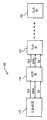
[0009]图1示出根据本发明的一个实施例的非易失性存储器系统。在所示系统100中,主控制器110可提供对编号为120至12n的、标记为#0、#1、...#n的、数量为n+1的闪速存储装置的总体控制。时钟信号CLK可由主控制器始发,并且传递给第一存储装置120,第一存储装置120将CLK传递给下一存储装置121,依此类推,直至CLK到达该链中的最后一个存储装置、即存储装置12n。数据可通过图中集中标记为DATA的多个并行数据线双向传递。并行数据线的数量可以是任何可行的量,例如但不限于4、8、16、32等。写数据可在主控制器中始发,并且从一个存储装置传递到另一存储装置,直至它到达指定存储装置为止,在指定存储装置将写数据写入该装置的内部存储器阵列。读数据可在所选存储装置中始发,并且通过多个存储器置直至到达主控制器为止,主控制器然后可处理该数据。到各种装置的电源连接未示出,以免使附图杂乱。[0009] FIG. 1 illustrates a non-volatile memory system according to one embodiment of the present invention. In the illustrated
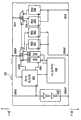
[0010]图2示出根据本发明的一个实施例的存储装置的框图。在所示实施例中,时钟、数据和数据有效(DV)线与图1中的时钟、数据和数据有效线对应。闪速存储装置编号为120,但是可对应于图1所示的任一闪速存储装置。闪存阵列230包括闪速存储装置的实际存储器部分,数据可存储在该部分中供其它装置使用。如图所示,在主控制器始发的时钟信号CLK可通过clkin输入来引入,并且用于给命令状态机240提供时钟,通过使用缓冲器210以便减小要是把所有存储装置直接连接到同一时钟线会引起的负载,还可将时钟信号从clkin传递到clkout。命令状态机240可用于根据通过data1线所引入的命令来控制闪速存储装置中的总体操作。[0010] FIG. 2 shows a block diagram of a storage device according to one embodiment of the present invention. In the illustrated embodiment, the clock, data, and data valid (DV) lines correspond to those of FIG. 1 . The flash memory device is numbered 120, but may correspond to any of the flash memory devices shown in FIG. 1 . Flash
[0011]为了便于描述,在本文档的上下文中,‘上游’表示朝主控制器移动的数据,而‘下游’表示远离主控制器移动的数据。例如,图1中,装置121将在装置120的下游,而装置120将在装置121的上游。主控制器110在所有存储装置12x的上游。[0011] For ease of description, in the context of this document, 'upstream' means data moving towards the main controller, and 'downstream' means data moving away from the main controller. For example, in FIG. 1 ,
[0012]参照图2,数据信号可去往上游或下游,并且可通过存储装置传递、或者始发于该存储装置始发或者指定给该存储装置。复用器/解复用器(mux/demux)271可用于在命令状态机240的控制下为这个装置与下一上游装置之间沿任一方向传播的数据提供适当的数据通路。mux/demux 271可将下游数据从data1路由到寄存器262,数据可锁存在寄存器262中并且在data2对下一下游装置可用。类似地,来自data2的、已锁存在寄存器261中的上游数据可通过mux/demux271而在data1可用于传递给下一上游装置。虽然mux/demux 271示为单个功能电路,但是在一些实施例中,它可实现为复用器和独立的解复用器。[0012] Referring to FIG. 2, the data signal may go upstream or downstream and may pass through, originate from, or be directed to the storage device. A multiplexer/demux (mux/demux) 271 may be used under the control of the
[0013]为了给传递数据提供适当时序,数据有效(DV)信号也可以任一方向传递,其中下游信号锁存在寄存器263中而上游信号锁存在寄存器264中。在某些情况下,例如当存储装置正从它自己的存储器阵列提供数据而不是传递来自另一存储装置的数据时,mux/demux272可设置成在DV1提供时序信号fclk,而不是传递来自下游装置的DV信号。在一些实施例中,信号fclk可以是在命令状态机240的控制下从clkin得出的、但仅在某些时间才是活动的时钟信号。[0013] To provide proper timing for transferring data, data valid (DV) signals may also be transferred in either direction, with the downstream signal latched in
[0014]当主控制器正尝试从这个特定闪速存储装置读取数据时,从闪存阵列230所读取的数据可放入先进先出缓冲器(FIFO)251,mux/demux 271可从所述先进先出缓冲器中选取数据以提供在data1供下一上游装置读取。当主控制器正尝试将数据写入这个特定存储装置时,在data1的数据可由mux/demux 271路由到FIFO 252,可将数据从FIFO 252写入闪存阵列。[0014] When the master controller is trying to read data from this particular flash memory device, the data read from the
[0015]FIFO可用于允许可具有较慢的数据传输率的阵列与可具有较高的数据传输率的菊花链总线之间的数据传输率的差异。在一些实施例中,一页(或其它块大小)数据在通过data1向上游传递之前可由阵列230完全写入FIFO 251。类似地,完整数据块可在从FIFO252写入阵列230之前通过data1写入FIFO 252。[0015] FIFOs can be used to allow differences in data transfer rates between arrays, which can have slower data transfer rates, and daisy-chain buses, which can have higher data transfer rates. In some embodiments, a page (or other block size) of data may be completely written to
[0016]这种在FIFO中进行缓冲的技术可有利地用来通过对一个存储装置执行操作的同时另一存储装置正用其FIFO进行内部传输而提高存储器系统的总吞吐量。例如,可指示存储装置#0从其阵列读取数据。当它正将那个数据从其阵列移到其FIFO时,存储装置#1可被指示从它自己的阵列读取数据。然后可对其它存储装置开始类似的读操作。到已经开始所有读操作时,存储装置#0可能已经填充其FIFO,并且可将那个数据传送给主控制器。当那个传输完成时,可指示存储装置#0从其阵列读取它将要开始放入其FIFO的另一数据块。这时,存储装置#1可能已经填充其FIFO,且可将那个数据传送给主控制器并被指示将另一数据块读入其FIFO。这个过程可对其余存储装置继续进行,直到它们均已将其数据传送给主控制器。那时,可指示存储装置#0将其第二数据块从其FIFO传送给主控制器,并且该过程可重复进行。在不同存储装置之间进行交替的这个过程可继续直到已经传送所有必要的数据。可通过将数据依次写入各存储装置的FIFO,并且在其它装置正从主控制器接收其数据的同时令一个装置将数据从其FIFO写入其阵列,接着对写操作进行类似的过程。虽然这个过程描述为按照采用菊花链方式连接在一起的顺序来选择存储装置,但是一些操作可按照不同顺序来选择装置。[0016] This technique of buffering in a FIFO can be advantageously used to increase the overall throughput of a memory system by performing operations on one memory device while another memory device is using its FIFO for internal transfers. For example,
[0017]应当注意,所有内部数据通路虽然在图中以单线表示,但是实际上可包含多个并行线,在一些实施例中,所述并行线可在数量上等于存储装置之间的并行数据线的数量。类似地,FIFO 251和252、寄存器261和262以及mux/demux 271可配置成处理所需数量的并行信号。[0017] It should be noted that all internal data paths, although shown as single lines in the figures, may actually consist of multiple parallel lines, which in some embodiments may be equal in number to the parallel data paths between storage devices. the number of lines. Similarly,
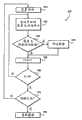
[0018]图3A、图3B和图3C示出根据本发明的一个实施例、由存储装置所执行的方法的流程图。在流程图300的所示实施例中,在310,存储装置接收命令。命令可以是若干不同类型的命令中之一。如在315所确定的,如果命令是寻址到另一存储装置的读命令,则在316,当前存储装置可将其内部复用器/解复用器(例如图2的mux/demux 271)配置用于读传递操作。当直接或者通过另一下游装置间接接收到来自所选下游存储装置的读数据时,在317,这个读数据可通过当前存储装置的控制电路向上游传递。[0018] FIG. 3A, FIG. 3B and FIG. 3C show a flowchart of a method performed by a storage device according to an embodiment of the present invention. In the illustrated embodiment of flowchart 300, at 310, a memory device receives a command. A command can be one of several different types of commands. As determined at 315, if the command is a read command addressed to another storage device, then at 316 the current storage device may use its internal multiplexer/demux (e.g., mux/
[0019]如在320所确定的,如果命令是对于另一装置的写命令,则在321,当前存储装置可将其mux/demux配置用于传递写操作。当直接或者通过另一上游装置间接接收到来自主控制器的写数据时,在322,这个写数据可通过当前存储装置的控制电路向下游传递。[0019] As determined at 320, if the command is a write command to another device, then at 321 the current storage device may configure its mux/demux to pass the write operation. When write data is received from the master controller either directly or indirectly through another upstream device, at 322 this write data may be passed downstream through the control circuitry of the current storage device.
[0020]如在325所确定的,如果命令是寻址到这个存储装置的读命令,则该过程可在图3B继续进行。在340,存储装置可将其mux/demux配置用于内部读取。如在345所确定的,如果先前所请求数据在FIFO中可用,则在350,那个数据可从那个FIFO发送给下一上游装置,可从所述下一上游装置将它传递给主控制器。如果FIFO为空,则在355,存储装置可使用读命令来触发数据从其自己的阵列到其FIFO的传送。一旦该存储装置在350已经完成向上游传送其FIFO数据,或者在355已经开始将数据从其阵列传送到其FIFO,则可返回到图3A中的‘A’以便等待下一命令。甚至在存储装置返回到A之后,在355的操作也可继续完成。[0020] As determined at 325, if the command is a read command addressed to this storage device, the process may continue at FIG. 3B. At 340, the storage device may configure its mux/demux for internal reads. As determined at 345, if the previously requested data is available in the FIFO, then at 350 that data may be sent from that FIFO to the next upstream device, from which it may be passed to the master controller. If the FIFO is empty, then at 355 the storage device can use a read command to trigger the transfer of data from its own array to its FIFO. Once the storage device has finished transferring its FIFO data upstream at 350, or has started transferring data from its array to its FIFO at 355, it may return to 'A' in Figure 3A to wait for the next command. Even after storage is returned to A, operations at 355 can continue to complete.
[0021]回到图3A,如在330所确定的,如果在310所示的命令是寻址到这个存储装置的写命令,则该过程可在图3C继续进行。在360,存储装置可将其mux/demux配置用于内部写入。如在365所确定的,如果FIFO因为仍然包含来自前一写操作的数据而没有预备接收更多数据,则该存储装置可不进行操作(除了继续将剩余数据从FIFO写入阵列之外),并且返回到A以便等待另一命令。如在365所确定的,如果FIFO预备接收数据,则在375,可从上游接收到那个数据并将其写入FIFO。一旦该数据处于FIFO中,则在380,可开始将那个数据写入阵列。一旦已经完成在375新数据到FIFO的传送,并且在380开始了数据到阵列的传送,则甚至在存储装置已经返回到A以便等待另一命令之后,也可继续完成数据到阵列的传送。[0021] Returning to FIG. 3A, as determined at 330, if the command shown at 310 is a write command addressed to this storage device, the process may continue at FIG. 3C. At 360, the storage device may configure its mux/demux for internal writes. As determined at 365, if the FIFO is not ready to receive more data because it still contains data from a previous write operation, the storage device may not operate (other than continue to write remaining data from the FIFO to the array), and Return to A to wait for another command. As determined at 365, if the FIFO is ready to receive data, then at 375 that data may be received from upstream and written to the FIFO. Once that data is in the FIFO, at 380, writing that data to the array can begin. Once the transfer of new data to the FIFO at 375 has been completed and the transfer of data to the array started at 380, the transfer of data to the array may continue to complete even after the storage device has returned to A to await another command.
[0022]如果在310接收到与刚才所述的四个命令不同的命令,则在335,存储装置可移动到需要的任何其它处理(未描述)。在一些实施例中,如果存储装置在接收到来自主控制器的命令时没有预备执行所述选项的任一个,则可返回‘忙’或‘错误’状态。[0022] If a different command than the four just described is received at 310, then at 335 the storage device may move to any other processing required (not depicted). In some embodiments, a 'busy' or 'error' status may be returned if the storage device is not ready to execute any of the options when it receives the command from the master controller.
[0023]图4示出根据本发明的一个实施例、由主控制器所执行的方法的流程图。在一些实施例中,这可以是图1的主控制器110。在所示流程图400中,在410,主控制器选择多个存储装置的第一存储装置,并且在420,在菊花链总线上发送寻址到那个存储装置的命令。为了描述的简洁起见,在这里用X=0至X=n的递增值表示对0至n的各存储装置依次寻址,但是其它实施例可使用其它过程来识别和选择各个存储装置。如在430所确定的,如果所选存储装置预备传送数据,则在440,主控制器可执行数据传输。‘预备传送数据’表示所选存储装置在其FIFO中具有预备传送给主控制器的数据(在读命令的情况下),或者所选存储装置具有预备接收来自主控制器的数据的可用FIFO(在写命令的情况下)。在450,主控制器可在数据传输之后(或者如果没有传送数据就立即)选择下一存储装置(X=X+1),并且对那个新选择的存储装置重复该过程。如在460所确定的,当已经通过这种方式与所有预期存储装置进行了通信时,主控制器可对第一存储装置继续进行操作,并且重复具有更多读或写数据的序列。如在470所确定的,当已经完成所有传输时,主控制器可继续进行其它处理。在一些实施例中,在读操作的情况下,在480,从数据传输到主控制器的所有数据可正确装配成单个数据块。将来的数据传输稍后可在410再次开始。类似地,在写操作的情况下,数据块最初可分成各个部分,其中的每个部分单独发送给各个存储装置中的各个FIFO。[0023] FIG. 4 shows a flowchart of a method performed by the main controller according to an embodiment of the present invention. In some embodiments, this may be
[0024]以上描述意在是说明性而不是限制性的。本领域的技术人员会想到一些变更。那些变更意在包含于发明的各种实施例中,本发明的各种实施例仅受到随附权利要求书的精神和范围限制。[0024] The above description is intended to be illustrative rather than limiting. Variations will occur to those skilled in the art. Those variations are intended to be included in various embodiments of the invention, which are limited only by the spirit and scope of the appended claims.
Claims (19)
Applications Claiming Priority (3)
| Application Number | Priority Date | Filing Date | Title |
|---|---|---|---|
| US11/644,270US7650459B2 (en) | 2006-12-21 | 2006-12-21 | High speed interface for non-volatile memory |
| US11/644,270 | 2006-12-21 | ||
| PCT/US2007/024346WO2008079189A1 (en) | 2006-12-21 | 2007-11-21 | High speed interface for non-volatile memory |
Related Child Applications (1)
| Application Number | Title | Priority Date | Filing Date |
|---|---|---|---|
| CN2011100426602ADivisionCN102156682B (en) | 2006-12-21 | 2007-11-21 | High speed interface for non-volatile memory |
Publications (2)
| Publication Number | Publication Date |
|---|---|
| CN101606137Atrue CN101606137A (en) | 2009-12-16 |
| CN101606137B CN101606137B (en) | 2015-01-14 |
Family
ID=39544599
Family Applications (2)
| Application Number | Title | Priority Date | Filing Date |
|---|---|---|---|
| CN200780046893.1AExpired - Fee RelatedCN101606137B (en) | 2006-12-21 | 2007-11-21 | High speed interface for non-volatile memory |
| CN2011100426602AExpired - Fee RelatedCN102156682B (en) | 2006-12-21 | 2007-11-21 | High speed interface for non-volatile memory |
Family Applications After (1)
| Application Number | Title | Priority Date | Filing Date |
|---|---|---|---|
| CN2011100426602AExpired - Fee RelatedCN102156682B (en) | 2006-12-21 | 2007-11-21 | High speed interface for non-volatile memory |
Country Status (5)
| Country | Link |
|---|---|
| US (1) | US7650459B2 (en) |
| KR (1) | KR101087419B1 (en) |
| CN (2) | CN101606137B (en) |
| TW (1) | TWI379302B (en) |
| WO (1) | WO2008079189A1 (en) |
Cited By (3)
| Publication number | Priority date | Publication date | Assignee | Title |
|---|---|---|---|---|
| CN102841872A (en)* | 2011-05-02 | 2012-12-26 | 西部数据技术公司 | High performance path for command processing |
| CN104216850A (en)* | 2013-05-31 | 2014-12-17 | 鸿富锦精密电子(天津)有限公司 | Interface transmission equipment |
| CN115801541A (en)* | 2022-11-18 | 2023-03-14 | 湖南长银五八消费金融股份有限公司 | Slow access warning method and device in full-link tracking platform and computer equipment |
Families Citing this family (17)
| Publication number | Priority date | Publication date | Assignee | Title |
|---|---|---|---|---|
| KR101293365B1 (en) | 2005-09-30 | 2013-08-05 | 모사이드 테크놀로지스 인코퍼레이티드 | Memory with output control |
| US7652922B2 (en) | 2005-09-30 | 2010-01-26 | Mosaid Technologies Incorporated | Multiple independent serial link memory |
| US20070165457A1 (en)* | 2005-09-30 | 2007-07-19 | Jin-Ki Kim | Nonvolatile memory system |
| WO2008101316A1 (en) | 2007-02-22 | 2008-08-28 | Mosaid Technologies Incorporated | Apparatus and method for using a page buffer of a memory device as a temporary cache |
| US8086785B2 (en) | 2007-02-22 | 2011-12-27 | Mosaid Technologies Incorporated | System and method of page buffer operation for memory devices |
| US8683126B2 (en)* | 2007-07-30 | 2014-03-25 | Nvidia Corporation | Optimal use of buffer space by a storage controller which writes retrieved data directly to a memory |
| KR101412524B1 (en)* | 2008-01-31 | 2014-06-25 | 삼성전자주식회사 | Memory device, memory card system and method of recognizing the card |
| US20110047318A1 (en)* | 2009-08-19 | 2011-02-24 | Dmitroca Robert W | Reducing capacitive load in a large memory array |
| US8464020B2 (en)* | 2009-12-07 | 2013-06-11 | Panasonic Corporation | Non-volatile storage device, host device, storage system, data communication method and program |
| US8208484B2 (en)* | 2010-01-11 | 2012-06-26 | Telefonaktiebolaget L M Ericsson (Publ) | Forwarding a packet within a router using fragments over an interconnect |
| US8843692B2 (en) | 2010-04-27 | 2014-09-23 | Conversant Intellectual Property Management Inc. | System of interconnected nonvolatile memories having automatic status packet |
| US8463959B2 (en) | 2010-05-31 | 2013-06-11 | Mosaid Technologies Incorporated | High-speed interface for daisy-chained devices |
| US8856482B2 (en) | 2011-03-11 | 2014-10-07 | Micron Technology, Inc. | Systems, devices, memory controllers, and methods for memory initialization |
| US9159647B2 (en) | 2012-01-27 | 2015-10-13 | Novachips Canada Inc. | Method and apparatus for connecting memory dies to form a memory system |
| US9471484B2 (en) | 2012-09-19 | 2016-10-18 | Novachips Canada Inc. | Flash memory controller having dual mode pin-out |
| WO2014143023A1 (en)* | 2013-03-15 | 2014-09-18 | Hewlett-Packard Development Company, L.P. | Memory module controller supporting extended writes |
| US10216685B1 (en)* | 2017-07-19 | 2019-02-26 | Agiga Tech Inc. | Memory modules with nonvolatile storage and rapid, sustained transfer rates |
Citations (1)
| Publication number | Priority date | Publication date | Assignee | Title |
|---|---|---|---|---|
| US20050120163A1 (en)* | 2003-12-02 | 2005-06-02 | Super Talent Electronics Inc. | Serial Interface to Flash-Memory Chip Using PCI-Express-Like Packets and Packed Data for Partial-Page Writes |
Family Cites Families (10)
| Publication number | Priority date | Publication date | Assignee | Title |
|---|---|---|---|---|
| US5860080A (en)* | 1996-03-19 | 1999-01-12 | Apple Computer, Inc. | Multicasting system for selecting a group of memory devices for operation |
| CN1188279A (en)* | 1996-11-26 | 1998-07-22 | 村田机械株式会社 | Host device and information processing device |
| US6378018B1 (en)* | 1997-10-10 | 2002-04-23 | Intel Corporation | Memory device and system including a low power interface |
| US6317352B1 (en)* | 2000-09-18 | 2001-11-13 | Intel Corporation | Apparatus for implementing a buffered daisy chain connection between a memory controller and memory modules |
| US6658509B1 (en)* | 2000-10-03 | 2003-12-02 | Intel Corporation | Multi-tier point-to-point ring memory interface |
| US6996644B2 (en)* | 2001-06-06 | 2006-02-07 | Conexant Systems, Inc. | Apparatus and methods for initializing integrated circuit addresses |
| US20050086413A1 (en)* | 2003-10-15 | 2005-04-21 | Super Talent Electronics Inc. | Capacity Expansion of Flash Memory Device with a Daisy-Chainable Structure and an Integrated Hub |
| US20060129701A1 (en)* | 2004-12-15 | 2006-06-15 | Shekoufeh Qawami | Communicating an address to a memory device |
| US20070076502A1 (en)* | 2005-09-30 | 2007-04-05 | Pyeon Hong B | Daisy chain cascading devices |
| US20070165457A1 (en)* | 2005-09-30 | 2007-07-19 | Jin-Ki Kim | Nonvolatile memory system |
- 2006
- 2006-12-21USUS11/644,270patent/US7650459B2/enactiveActive
- 2007
- 2007-11-21CNCN200780046893.1Apatent/CN101606137B/ennot_activeExpired - Fee Related
- 2007-11-21WOPCT/US2007/024346patent/WO2008079189A1/enactiveApplication Filing
- 2007-11-21CNCN2011100426602Apatent/CN102156682B/ennot_activeExpired - Fee Related
- 2007-11-21KRKR1020097012859Apatent/KR101087419B1/ennot_activeExpired - Fee Related
- 2007-11-22TWTW096144255Apatent/TWI379302B/ennot_activeIP Right Cessation
Patent Citations (1)
| Publication number | Priority date | Publication date | Assignee | Title |
|---|---|---|---|---|
| US20050120163A1 (en)* | 2003-12-02 | 2005-06-02 | Super Talent Electronics Inc. | Serial Interface to Flash-Memory Chip Using PCI-Express-Like Packets and Packed Data for Partial-Page Writes |
Cited By (5)
| Publication number | Priority date | Publication date | Assignee | Title |
|---|---|---|---|---|
| CN102841872A (en)* | 2011-05-02 | 2012-12-26 | 西部数据技术公司 | High performance path for command processing |
| CN102841872B (en)* | 2011-05-02 | 2017-09-22 | 西部数据技术公司 | High-performance path for command process |
| CN104216850A (en)* | 2013-05-31 | 2014-12-17 | 鸿富锦精密电子(天津)有限公司 | Interface transmission equipment |
| CN115801541A (en)* | 2022-11-18 | 2023-03-14 | 湖南长银五八消费金融股份有限公司 | Slow access warning method and device in full-link tracking platform and computer equipment |
| CN115801541B (en)* | 2022-11-18 | 2024-03-22 | 湖南长银五八消费金融股份有限公司 | Method and device for alarming slow access in full-link tracking platform and computer equipment |
Also Published As
| Publication number | Publication date |
|---|---|
| US20080155207A1 (en) | 2008-06-26 |
| TW200832415A (en) | 2008-08-01 |
| KR20090080568A (en) | 2009-07-24 |
| CN102156682A (en) | 2011-08-17 |
| TWI379302B (en) | 2012-12-11 |
| CN102156682B (en) | 2013-03-06 |
| CN101606137B (en) | 2015-01-14 |
| US7650459B2 (en) | 2010-01-19 |
| WO2008079189A1 (en) | 2008-07-03 |
| KR101087419B1 (en) | 2011-11-25 |
Similar Documents
| Publication | Publication Date | Title |
|---|---|---|
| CN101606137B (en) | High speed interface for non-volatile memory | |
| US7567471B2 (en) | High speed fanned out system architecture and input/output circuits for non-volatile memory | |
| CN1828511B (en) | Solid state disk controller apparatus and operation method | |
| US10224080B2 (en) | Semiconductor memory device with late write feature | |
| JP2007087388A (en) | Memory controller and data processing system including the same | |
| CN102541678B (en) | Multichannel NAND flash parallel memory controller | |
| US9792072B2 (en) | Embedded multimedia card (eMMC), host controlling eMMC, and method operating eMMC system | |
| JP4621604B2 (en) | Bus device, bus system, and information transfer method | |
| KR20120015313A (en) | Memory Controllers, Memory Systems, Solid State Drivers, and Methods for Processing Multiple Instructions | |
| KR20080048534A (en) | Portable data storage device and method using SLC and MLC flash memory | |
| CN114625678A (en) | memory system | |
| US20140013041A1 (en) | Simultaneous read and write data transfer | |
| CN102567258B (en) | Multi-dimensional DMA (direct memory access) transmitting device and method | |
| CN103811080A (en) | Memory test system and memory test method | |
| JP5643896B2 (en) | High speed interface for daisy chained devices | |
| US9990159B2 (en) | Apparatus, system, and method of look-ahead address scheduling and autonomous broadcasting operation to non-volatile storage memory | |
| US7913013B2 (en) | Semiconductor integrated circuit | |
| US9965193B2 (en) | Apparatus, system, and method of sequencing, shadowing, and queuing operations in a non-volatile storage memory | |
| KR20130091377A (en) | Non-volatile memory system and method of controlling a data transfer delay in the same | |
| JP2022002164A (en) | Non-sequential page continuous reading | |
| US7574548B2 (en) | Dynamic data transfer control method and apparatus for shared SMP computer systems | |
| US20160004655A1 (en) | Computing system and operating method of the same | |
| KR100761374B1 (en) | Flash memory control method and device | |
| JP2012018639A (en) | Memory system and nonvolatile semiconductor memory |
Legal Events
| Date | Code | Title | Description |
|---|---|---|---|
| C06 | Publication | ||
| PB01 | Publication | ||
| C10 | Entry into substantive examination | ||
| SE01 | Entry into force of request for substantive examination | ||
| C14 | Grant of patent or utility model | ||
| GR01 | Patent grant | ||
| CF01 | Termination of patent right due to non-payment of annual fee | Granted publication date:20150114 Termination date:20181121 | |
| CF01 | Termination of patent right due to non-payment of annual fee |