CN101604703B - Organic light emitting diode display device and method of manufacturing the same - Google Patents
Organic light emitting diode display device and method of manufacturing the sameDownload PDFInfo
- Publication number
- CN101604703B CN101604703BCN2009101420540ACN200910142054ACN101604703BCN 101604703 BCN101604703 BCN 101604703BCN 2009101420540 ACN2009101420540 ACN 2009101420540ACN 200910142054 ACN200910142054 ACN 200910142054ACN 101604703 BCN101604703 BCN 101604703B
- Authority
- CN
- China
- Prior art keywords
- light
- emitting
- sub
- emitting layer
- pixel
- Prior art date
- Legal status (The legal status is an assumption and is not a legal conclusion. Google has not performed a legal analysis and makes no representation as to the accuracy of the status listed.)
- Active
Links
- 238000004519manufacturing processMethods0.000titledescription8
- 238000000034methodMethods0.000claimsabstractdescription10
- 230000008021depositionEffects0.000claimsdescription10
- 239000003086colorantSubstances0.000claimsdescription2
- 239000010410layerSubstances0.000description250
- 239000000463materialSubstances0.000description25
- 238000000151depositionMethods0.000description19
- 239000000758substrateSubstances0.000description14
- 239000010409thin filmSubstances0.000description14
- 229910052782aluminiumInorganic materials0.000description5
- XFXPMWWXUTWYJX-UHFFFAOYSA-NCyanideChemical compoundN#[C-]XFXPMWWXUTWYJX-UHFFFAOYSA-N0.000description4
- PXGOKWXKJXAPGV-UHFFFAOYSA-NFluorineChemical compoundFFPXGOKWXKJXAPGV-UHFFFAOYSA-N0.000description4
- 125000004093cyano groupChemical group*C#N0.000description4
- 229910052731fluorineInorganic materials0.000description4
- 239000011737fluorineSubstances0.000description4
- 125000000956methoxy groupChemical group[H]C([H])([H])O*0.000description4
- 239000010408filmSubstances0.000description3
- 229910052749magnesiumInorganic materials0.000description3
- 239000000203mixtureSubstances0.000description3
- XLOMVQKBTHCTTD-UHFFFAOYSA-Nzinc oxideInorganic materials[Zn]=OXLOMVQKBTHCTTD-UHFFFAOYSA-N0.000description3
- 239000011787zinc oxideSubstances0.000description3
- VYPSYNLAJGMNEJ-UHFFFAOYSA-NSilicium dioxideChemical compoundO=[Si]=OVYPSYNLAJGMNEJ-UHFFFAOYSA-N0.000description2
- XUIMIQQOPSSXEZ-UHFFFAOYSA-NSiliconChemical compound[Si]XUIMIQQOPSSXEZ-UHFFFAOYSA-N0.000description2
- 238000002347injectionMethods0.000description2
- 239000007924injectionSubstances0.000description2
- 239000004065semiconductorSubstances0.000description2
- 229910052710siliconInorganic materials0.000description2
- 239000010703siliconSubstances0.000description2
- 229910052779NeodymiumInorganic materials0.000description1
- 229910052581Si3N4Inorganic materials0.000description1
- 230000015572biosynthetic processEffects0.000description1
- 229910052804chromiumInorganic materials0.000description1
- 230000000593degrading effectEffects0.000description1
- 238000010586diagramMethods0.000description1
- 230000005684electric fieldEffects0.000description1
- 239000007772electrode materialSubstances0.000description1
- 239000011521glassSubstances0.000description1
- 229910052737goldInorganic materials0.000description1
- 230000005525hole transportEffects0.000description1
- AMGQUBHHOARCQH-UHFFFAOYSA-Nindium;oxotinChemical compound[In].[Sn]=OAMGQUBHHOARCQH-UHFFFAOYSA-N0.000description1
- 239000011229interlayerSubstances0.000description1
- 229910052741iridiumInorganic materials0.000description1
- 229910052759nickelInorganic materials0.000description1
- 239000011368organic materialSubstances0.000description1
- 229910052763palladiumInorganic materials0.000description1
- 229910052697platinumInorganic materials0.000description1
- 235000012239silicon dioxideNutrition0.000description1
- 239000000377silicon dioxideSubstances0.000description1
- HQVNEWCFYHHQES-UHFFFAOYSA-Nsilicon nitrideChemical compoundN12[Si]34N5[Si]62N3[Si]51N64HQVNEWCFYHHQES-UHFFFAOYSA-N0.000description1
- 229910052709silverInorganic materials0.000description1
- YVTHLONGBIQYBO-UHFFFAOYSA-Nzinc indium(3+) oxygen(2-)Chemical compound[O--].[Zn++].[In+3]YVTHLONGBIQYBO-UHFFFAOYSA-N0.000description1
Images


Classifications
- H—ELECTRICITY
- H10—SEMICONDUCTOR DEVICES; ELECTRIC SOLID-STATE DEVICES NOT OTHERWISE PROVIDED FOR
- H10K—ORGANIC ELECTRIC SOLID-STATE DEVICES
- H10K59/00—Integrated devices, or assemblies of multiple devices, comprising at least one organic light-emitting element covered by group H10K50/00
- H10K59/30—Devices specially adapted for multicolour light emission
- H10K59/35—Devices specially adapted for multicolour light emission comprising red-green-blue [RGB] subpixels
- H—ELECTRICITY
- H10—SEMICONDUCTOR DEVICES; ELECTRIC SOLID-STATE DEVICES NOT OTHERWISE PROVIDED FOR
- H10K—ORGANIC ELECTRIC SOLID-STATE DEVICES
- H10K50/00—Organic light-emitting devices
- H10K50/10—OLEDs or polymer light-emitting diodes [PLED]
- H10K50/14—Carrier transporting layers
- H10K50/15—Hole transporting layers
- H—ELECTRICITY
- H10—SEMICONDUCTOR DEVICES; ELECTRIC SOLID-STATE DEVICES NOT OTHERWISE PROVIDED FOR
- H10K—ORGANIC ELECTRIC SOLID-STATE DEVICES
- H10K50/00—Organic light-emitting devices
- H10K50/10—OLEDs or polymer light-emitting diodes [PLED]
- H10K50/14—Carrier transporting layers
- H10K50/16—Electron transporting layers
- H—ELECTRICITY
- H10—SEMICONDUCTOR DEVICES; ELECTRIC SOLID-STATE DEVICES NOT OTHERWISE PROVIDED FOR
- H10K—ORGANIC ELECTRIC SOLID-STATE DEVICES
- H10K59/00—Integrated devices, or assemblies of multiple devices, comprising at least one organic light-emitting element covered by group H10K50/00
- H10K59/10—OLED displays
- H10K59/12—Active-matrix OLED [AMOLED] displays
- H10K59/122—Pixel-defining structures or layers, e.g. banks
- H—ELECTRICITY
- H01—ELECTRIC ELEMENTS
- H01L—SEMICONDUCTOR DEVICES NOT COVERED BY CLASS H10
- H01L2924/00—Indexing scheme for arrangements or methods for connecting or disconnecting semiconductor or solid-state bodies as covered by H01L24/00
- H01L2924/10—Details of semiconductor or other solid state devices to be connected
- H01L2924/11—Device type
- H01L2924/13—Discrete devices, e.g. 3 terminal devices
- H01L2924/1304—Transistor
- H01L2924/1306—Field-effect transistor [FET]
- H01L2924/13069—Thin film transistor [TFT]
Landscapes
- Physics & Mathematics (AREA)
- Optics & Photonics (AREA)
- Engineering & Computer Science (AREA)
- Microelectronics & Electronic Packaging (AREA)
- Electroluminescent Light Sources (AREA)
- Devices For Indicating Variable Information By Combining Individual Elements (AREA)
Abstract
Translated fromChineseDescription
Translated fromChinese技术领域technical field
实例实施例涉及有机发光二极管显示设备。更具体地,实例实施例涉及高分辨率的有机发光二极管显示设备,其中每个子像素的发光层容易沉积,并且子像素的图样的精度被提高。Example embodiments relate to organic light emitting diode display devices. More particularly, example embodiments relate to a high resolution organic light emitting diode display device in which a light emitting layer of each sub-pixel is easily deposited and the accuracy of patterns of the sub-pixels is improved.
背景技术Background technique
由于有机发光二极管(OLED)显示设备具有宽视角、良好的对比度以及高响应速度,所以它们被认为是下一代显示设备。Organic light emitting diode (OLED) display devices are considered to be next-generation display devices because they have a wide viewing angle, good contrast ratio, and high response speed.
OLED显示设备可以包括彼此面对的第一电极和第二电极以及中间层,该中间层至少包括第一电极和第二电极之间的发光层。第一电极、第二电极以及中间层可以使用诸如沉积方法之类的各种方法来形成。当使用沉积方法时,使用了具有开口部分的掩模,该掩模的开口部分具有与待沉积的膜的图样相同的图样。该掩模可以紧密地粘附于膜将被形成在的表面,并且材料可以通过该掩模沉积在该表面上,以形成具有预定图样的薄膜。The OLED display device may include first and second electrodes facing each other and an intermediate layer including at least a light emitting layer between the first and second electrodes. The first electrode, the second electrode, and the intermediate layer may be formed using various methods such as a deposition method. When using the deposition method, a mask having an opening portion having the same pattern as that of the film to be deposited is used. The mask can be closely adhered to the surface on which the film is to be formed, and material can be deposited on the surface through the mask to form a thin film having a predetermined pattern.
当常规OLED显示设备包括多个像素时,例如,每个像素包括红子像素、绿子像素和蓝子像素,可以利用沉积方法来形成这些子像素的发光层。例如,可以通过同时通过掩模的沉积来形成所有发红光的子像素的发光层,而后可以通过同时沉积来形成所有发蓝光的子像素的发光层,而后可以通过同时沉积来形成所有发绿光的子像素的发光层。When a conventional OLED display device includes a plurality of pixels, for example, each pixel includes a red sub-pixel, a green sub-pixel and a blue sub-pixel, a deposition method may be used to form the light emitting layers of these sub-pixels. For example, the emissive layers of all red-emitting sub-pixels can be formed by simultaneous deposition through a mask, then all blue-emitting sub-pixels can be formed by simultaneous deposition, and then all green-emitting sub-pixels can be formed by simultaneous deposition. The light-emitting layer of the sub-pixel.
然而,由于为了制造具有高图像质量的显示设备,相邻的子像素之间的距离变短,所以用于沉积子像素发光层的掩摸的开口部分之间的距离也可能被缩短。例如,如果红子像素、绿子像素和蓝子像素沿第一方向以此顺序重复形成,那么,在分辨率为140ppi的QCIF OLED中,用于蓝发光层的掩模的两个相邻的开口部分之间沿第一方向的距离可以为约0.068mm,即发蓝光的两个相邻的子像素之间沿第一方向的距离。尽管常规的微小节距掩模,例如相邻的开口部分之间的距离为大约0.068mm的掩模,可能便于制造具有高图像质量的OLED显示设备,然而在制造这种细距掩模时可能存在许多限制,例如物理限制。另外,随着掩模的节距缩短,可能难于对掩模进行图样定制以及将掩模的图样与OLED显示设备的相应部分,即将要沉积发光层的部分对准。掩模的不精确对准和图样定制可以导致发光层的膜沉积不精确,从而降低了OLED显示设备的显示特性和图像质量。However, since the distance between adjacent sub-pixels is shortened in order to manufacture a display device with high image quality, the distance between opening portions of a mask for depositing a sub-pixel light emitting layer may also be shortened. For example, if red sub-pixels, green sub-pixels, and blue sub-pixels are repeatedly formed in this order along the first direction, then, in a QCIF OLED with a resolution of 140ppi, two adjacent layers of the mask for the blue light-emitting layer The distance between the opening portions along the first direction may be about 0.068 mm, that is, the distance along the first direction between two adjacent sub-pixels emitting blue light. Although a conventional fine-pitch mask, such as a mask with a distance between adjacent opening portions of about 0.068 mm, may facilitate the manufacture of an OLED display device with high image quality, it may be possible to manufacture such a fine-pitch mask. There are many limitations, such as physical limitations. In addition, as the pitch of the mask shrinks, it may be difficult to pattern the mask and align the pattern of the mask with the corresponding portion of the OLED display device, ie, the portion where the light emitting layer is to be deposited. Imprecise alignment and pattern customization of the mask can lead to imprecise film deposition of the light emitting layer, thereby degrading the display characteristics and image quality of the OLED display device.
发明内容Contents of the invention
因此,实例实施例致力于一种OLED显示设备及其制造方法,其基本上克服了由于现有技术的限制和缺点造成的一个以上问题。Accordingly, example embodiments are directed to an OLED display device and a method of fabricating the same, which substantially overcome the one or more problems due to limitations and disadvantages of the related art.
因此,实例实施例的特点是提供一种OLED显示设备,该OLED显示设备具有以提高的精度提供改进的沉积的子像素的设置。It is therefore a feature of example embodiments to provide an OLED display device having an arrangement of sub-pixels that provides improved deposition with increased precision.
因此,实例实施例的另一特点是提供一种制造OLED显示设备的方法,该方法通过设置其中的子像素来提供改进的沉积和精度。Accordingly, another feature of example embodiments is to provide a method of manufacturing an OLED display device that provides improved deposition and precision by arranging sub-pixels therein.
上述或其它特点和优点中的至少一个可以通过提供一种OLED显示设备来实现,该OLED显示设备包括多个像素,其中每个像素包括沿第一方向按顺序或者相反顺序分别发红光、蓝光和绿光的子像素,其中沿该有机发光显示设备的第一方向在像素中形成的子像素被布置成使得从一个像素的每个子像素发出的光的颜色的设置与从邻居像素的每个子像素发出的光的颜色的设置关于沿所述第一方向的像素之间的空间对称,并且其中发红光的子像素的发光层包括发红光的发光层和发绿光的发光层,并且发绿光的子像素的发光层包括发绿光的发光层,发蓝光的子像素的发光层包括发蓝光的发光层和发绿光的发光层。At least one of the above or other features and advantages can be achieved by providing an OLED display device, the OLED display device includes a plurality of pixels, wherein each pixel includes an LED that emits red light and blue light respectively in sequence or in reverse order along the first direction. and green sub-pixels, wherein the sub-pixels formed in the pixels along the first direction of the organic light-emitting display device are arranged such that the color of light emitted from each sub-pixel of one pixel is set to be the same as that from each sub-pixel of a neighboring pixel The arrangement of the color of the light emitted by the pixels is symmetrical with respect to the space between the pixels along the first direction, and wherein the light-emitting layer of the red-emitting sub-pixel comprises a red-emitting light-emitting layer and a green-emitting light-emitting layer, and The light-emitting layer of the sub-pixel that emits green light includes a light-emitting layer that emits green light, and the light-emitting layer of the sub-pixel that emits blue light includes a light-emitting layer that emits blue light and a light-emitting layer that emits green light.
每个子像素可以包括彼此面对的第一电极和第二电极,并且每个子像素的发光层插在所述第一电极与所述第二电极之间,并且其中关于沿所述第一方向的两个彼此相邻的像素之间的空间彼此相邻的两个子像素的发红光的发光层或发蓝光的发光层形成为一个单元。Each sub-pixel may include a first electrode and a second electrode facing each other, and a light emitting layer of each sub-pixel is interposed between the first electrode and the second electrode, and wherein The red light-emitting light-emitting layer or the blue light-emitting light-emitting layer of two sub-pixels adjacent to each other in a space between two mutually adjacent pixels is formed as one unit.
多个所述子像素的发绿光的发光层可以形成为一个单元。The green light emitting layers of a plurality of the sub-pixels may be formed as one unit.
每个子像素可以包括彼此面对的阳极和阴极,每个子像素的发光层插在所述阳极与所述阴极之间,所述发红光的子像素的发红光的发光层可以布置在所述发红光的子像素的发绿光的发光层与所述阳极之间,并且所述发蓝光的子像素的发蓝光的发光层可以布置在所述发蓝光的子像素的发绿光的发光层与所述阳极之间。Each subpixel may include an anode and a cathode facing each other, a light emitting layer of each subpixel is interposed between the anode and the cathode, and the red light emitting layer of the red light emitting subpixel may be arranged on the between the green light-emitting layer of the red light-emitting sub-pixel and the anode, and the blue light-emitting layer of the blue light-emitting sub-pixel may be disposed between the green light-emitting layer of the blue light-emitting sub-pixel Between the light-emitting layer and the anode.
所述发红光的子像素的所述发红光的发光层的空穴迁移率可以低于其发绿光的发光层的空穴迁移率,并且其发绿光的发光层的电子迁移率可以高于其发红光的发光层的电子迁移率。The hole mobility of the red light emitting layer of the red light emitting sub-pixel may be lower than the hole mobility of the green light emitting layer thereof, and the electron mobility of the green light emitting layer thereof may be lower than that of the green light emitting layer. The electron mobility of the emitting layer which can be higher than its red emission.
所述发蓝光的子像素的发蓝光的发光层的空穴迁移率可以低于其发绿光的发光层的空穴迁移率,并且其发绿光的发光层的电子迁移率可以高于其发蓝光的发光层的电子迁移率。The blue light emitting sub-pixel may have a hole mobility of a blue light emitting layer lower than that of its green light emitting layer, and a green light emitting layer thereof may have an electron mobility higher than that of its green light emitting layer. Electron mobility of the blue emitting layer.
每个子像素可以包括彼此面对的阳极和阴极,并且每个子像素的发光层插在所述阳极与所述阴极之间,所述发红光的子像素的发绿光的发光层可以布置在所述发红光的子像素的发红光的发光层与所述阳极之间,并且所述发蓝光的子像素的发绿光的发光层可以布置所述发蓝光的子像素的发蓝光的发光层与所述阳极之间。Each subpixel may include an anode and a cathode facing each other, and a light emitting layer of each subpixel is interposed between the anode and the cathode, and the green light emitting layer of the red light emitting subpixel may be disposed on Between the red-emitting light-emitting layer of the red-emitting sub-pixel and the anode, and the green-emitting light-emitting layer of the blue-emitting sub-pixel, the blue light-emitting layer of the blue light-emitting sub-pixel may be arranged Between the light-emitting layer and the anode.
所述发红光的子像素的发红光的发光层的电子迁移率可以低于其发绿光的发光层的电子迁移率,并且其发绿光的发光层的空穴迁移率可以高于其发红光的发光层的空穴迁移率。The electron mobility of the red light emitting layer of the red light emitting sub-pixel may be lower than that of the green light emitting layer thereof, and the hole mobility of the green light emitting layer thereof may be higher than The hole mobility of its red-emitting emitting layer.
所述发蓝光的子像素的发蓝光的发光层的电子迁移率可以低于其发绿光的发光层的电子迁移率,并且其发绿光的发光层的空穴迁移率可以高于其发蓝光的发光层的空穴迁移率。The electron mobility of the blue light emitting layer of the blue light emitting subpixel may be lower than that of its green light emitting layer, and the hole mobility of its green light emitting layer may be higher than that of its green light emitting layer. Hole mobility of the emissive layer for blue light.
垂直于所述第一方向的第二方向上的子像素可以发出相同颜色的光。Sub-pixels in a second direction perpendicular to the first direction may emit light of the same color.
每个子像素可以包括彼此面对的第一电极和第二电极,并且每个子像素的发光层可以插在所述第一电极和所述第二电极之间,并且关于沿所述第一方向的两个彼此相邻的像素之间的空间彼此相邻的子像素中的两个的发红光或者蓝光的发光层可以形成为一个单元。Each sub-pixel may include a first electrode and a second electrode facing each other, and a light emitting layer of each sub-pixel may be interposed between the first electrode and the second electrode, and with respect to The red or blue light emitting layers of two adjacent sub-pixels in a space between two mutually adjacent pixels may be formed as one unit.
在所述第二方向上的子像素的发光层可以形成为一个单元。沿所述第一方向的子像素设置关于从相应子像素发出的光的颜色可以包括红、绿、蓝、蓝、绿、红、红、绿、蓝、蓝等等的顺序。The light emitting layers of the sub-pixels in the second direction may be formed as one unit. The arrangement of subpixels along the first direction may include an order of red, green, blue, blue, green, red, red, green, blue, blue, etc. with respect to colors of light emitted from corresponding subpixels.
上述或其它特点和优点中的至少一个可以通过提供一种形成OLED显示设备的方法来实现,该方法包括:形成包括按沿第一方向的预定顺序设置的子像素的多个像素,每个子像素发红光、绿光或者蓝光,并且所述预定顺序的子像素包括按沿所述第一方向发红光、绿光和蓝光的顺序或按相反顺序设置的子像素,其中沿所述第一方向在所述像素中形成的所述子像素被布置成使得从一个像素的子像素发出的光的颜色的设置与从沿所述第一方向的相邻像素的子像素发出的光的颜色的设置对称,对称设置的对称轴为这两个彼此相邻的像素之间的空间,并且其中所述发红光的子像素的发光层被形成为包括发红光的发光层和发绿光的发光层,所述发绿光的子像素的发光层被形成为包括发绿光的发光层,并且所述发蓝光的子像素的发光层被形成为包括发蓝光的发光层和发绿光的发光层。At least one of the above or other features and advantages can be achieved by providing a method of forming an OLED display device, the method comprising: forming a plurality of pixels including sub-pixels arranged in a predetermined order along a first direction, each sub-pixel emit red light, green light or blue light, and the sub-pixels in the predetermined order include sub-pixels arranged in the order of emitting red light, green light and blue light along the first direction or in the reverse order, wherein along the first direction The sub-pixels formed in the pixel are arranged such that the color of light emitted from the sub-pixels of one pixel is set differently from the color of light emitted from the sub-pixels of adjacent pixels along the first direction. The arrangement is symmetrical, and the symmetry axis of the symmetrical arrangement is the space between the two pixels adjacent to each other, and wherein the light-emitting layer of the red-light-emitting sub-pixel is formed to include a red-light-emitting light-emitting layer and a green-light-emitting a light-emitting layer, the light-emitting layer of the green light-emitting sub-pixel is formed to include a green light-emitting light-emitting layer, and the light-emitting layer of the blue light-emitting sub-pixel is formed to include a blue light-emitting light-emitting layer and a green light-emitting luminous layer.
形成每个子像素可以包括在第一电极和第二电极之间形成发光层,沿所述第一方向彼此相邻的相应像素的两个相邻的子像素的发红光的发光层或者发蓝光的发光层通过沉积掩模中的单个开口被形成为一个单元。发绿光的发光层可以被形成为一个单元。第二方向上的子像素被设置为发相同颜色的光,所述第二方向垂直于所述第一方向。所述第二方向上的子像素的发光层被形成为一个单元。Forming each sub-pixel may include forming a light-emitting layer between the first electrode and the second electrode, the red light-emitting light-emitting layer or the blue light-emitting light-emitting layer of two adjacent sub-pixels of corresponding pixels adjacent to each other along the first direction. The light-emitting layer is formed as a unit through a single opening in the deposition mask. The green light emitting layer may be formed as one unit. Sub-pixels in a second direction are arranged to emit light of the same color, the second direction being perpendicular to the first direction. The light emitting layers of the sub-pixels in the second direction are formed as a unit.
附图说明Description of drawings
通过参照附图对示例性实施例进行详细描述,上述和其它特征和优点对本领域技术人员将变得更加明显,在附图中:The above and other features and advantages will become more apparent to those skilled in the art by describing in detail exemplary embodiments with reference to the accompanying drawings, in which:
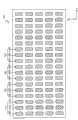
图1示出常规OLED显示设备的发光层的图样的平面图;1 shows a plan view of a pattern of a light emitting layer of a conventional OLED display device;
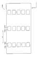
图2示出用于沉积图1的OLED显示设备的蓝发光层的常规掩模的平面图;2 shows a plan view of a conventional mask for depositing a blue light-emitting layer of the OLED display device of FIG. 1;
图3示出根据实例实施例的OLED显示设备的发光层的图样的平面图;3 illustrates a plan view of a pattern of a light emitting layer of an OLED display device according to an example embodiment;
图4示出图3的OLED的多个子像素的横截面图;Figure 4 shows a cross-sectional view of a plurality of sub-pixels of the OLED of Figure 3;
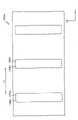
图5示出用于沉积图3的OLED显示设备的蓝发光层的掩模的平面图;5 shows a plan view of a mask for depositing a blue light-emitting layer of the OLED display device of FIG. 3;
图6示出用于沉积图3的OLED显示设备的绿发光层的掩模的另一实例实施例的平面图;和6 illustrates a plan view of another example embodiment of a mask for depositing a green light-emitting layer of the OLED display device of FIG. 3; and
图7示出根据另一实例实施例的OLED显示设备的多个子像素的横截面图。FIG. 7 illustrates a cross-sectional view of a plurality of subpixels of an OLED display device according to another example embodiment.
具体实施方式Detailed ways
2008年6月11日递交到韩国知识产权局的题目为“Organic LightEmitting Display(有机发光显示器)”的韩国专利申请No.10-2008-0054858以其整体通过引用合并于此。Korean Patent Application No. 10-2008-0054858, filed with the Korean Intellectual Property Office on Jun. 11, 2008, and entitled "Organic Light Emitting Display," is hereby incorporated by reference in its entirety.
在下文中,将参照附图更加充分地描述实例实施例;然而,这些实例实施例可以用不同的形式来实施并且不应被解释为限于在此阐述的实施例。相反,这些实施例被提供以便使该公开内容全面和完整,并且将向本领域技术人员充分传达本发明的范围。Hereinafter, example embodiments will be described more fully with reference to the accompanying drawings; however, these example embodiments may be embodied in different forms and should not be construed as limited to the embodiments set forth herein. Rather, these embodiments are provided so that this disclosure will be thorough and complete, and will fully convey the scope of the invention to those skilled in the art.
在附图中,为了示例的清楚起见,可以夸大层和区域的尺寸。还应理解的是,当层或元件被称为在另一层或者基板“上”时,它可以直接在其它层或者基板上,也可以存在中间层。进一步,应理解的是,当层被称为在另一层“下”时,它可以直接在另一层下,也可以存在一个以上中间层。另外,还应理解的是,当层被称为在两层“之间”时,它可以是这两层之间的唯一层,也可以存在一个以上中间层。在整个申请文件中,相同的附图标记指示相同元件。In the drawing figures, the dimensions of layers and regions may be exaggerated for clarity of illustration. It will also be understood that when a layer or element is referred to as being "on" another layer or substrate, it can be directly on the other layer or substrate, or intervening layers may also be present. Further, it will be understood that when a layer is referred to as being 'under' another layer, it can be directly under, and one or more intervening layers may also be present. In addition, it will also be understood that when a layer is referred to as being "between" two layers, it can be the only layer between the two layers, or more than one intervening layers may also be present. Throughout the application, like reference numerals refer to like elements.
图3示出根据实例实施例的OLED显示设备100的发光层的示意性设置的平面图,图4示出图3的OLED显示设备100的多个子像素的横截面图。图3示出OLED显示设备100的发光层的图样,而且为了便于理解,它还可以被看作是示出子像素中的每一个。它还适用于后面描述的实施例。3 illustrates a plan view of a schematic arrangement of light emitting layers of the
参见图3,OLED显示设备100可以包括多个像素110、120、130以及140。这些像素中的每一个都可以包括沿第一方向,例如沿图3中的x方向的发红光的子像素、发绿光的子像素以及发蓝光的子像素。多个像素可以各自包括沿第一方向按该顺序或者按相反顺序的发红光、发绿光以及发蓝光的多个相应的子像素。OLED显示设备100的包括沿第一方向(x方向)的像素中的子像素可以被布置成使得每个像素中子像素的设置可以与相邻像素中的子像素的设置关于沿第一方向的这两个相邻的像素之间的空间对称。Referring to FIG. 3 , the
例如,像素110、120、130以及140可以沿第一方向,即图3的x方向被设置成一行,并且可以包括沿x方向的发红光、绿光以及蓝光的子像素。假定布置在图3中示出的发光层(子像素)的图样的最上面的一行的像素各为第一像素110、第二像素120、第三像素130以及第四像素140,那么第一像素110可以包括沿x方向的发红光的子像素110R、发绿光的子像素110G以及发蓝光的子像素110B。For example, the
类似地,第二像素120、第三像素130以及第四像素140可以包括子像素。与第一像素110相邻的第二像素120的子像素120R、120G以及120B可以被设置为与第一像素110的子像素110R、110G以及110B关于第一像素110和第二像素120之间的空间对称。换句话说,第二像素120的分别发红光、绿光以及蓝光的子像素120R、120G以及120B可以被设置为与第一像素110的分别发红光、绿光以及蓝光的子像素110R、110G以及110B关于第一像素110和第二像素120之间的空间对称。相应地,如在图3所示,当第一像素110包括沿x方向的发红光的子像素110R、发绿光的子像素110G以及发蓝光的子像素110B时,与第一像素110相邻的第二像素120可以包括沿x方向的发蓝光的子像素120B、发绿光的子像素120G以及发红光的子像素120R。换句话说,如图3所示,第一像素110和第二像素120的子像素可以被设置成使得第一像素110和第二像素120各自的发蓝光的子像素110B和120B可以彼此相邻。Similarly, the
同样,第三像素130的分别发红光、绿光以及蓝光的子像素130R、130G以及130B可以设置为与第二像素120的子像素120R、120G以及120B的设置关于第二像素120和第三像素130之间的空间对称。相应地,如图3所示,当第二像素120包括沿x方向的发蓝光的子像素120B、发绿光的子像素120G以及发红光的子像素120R时,与第二像素120相邻的第三像素130可以包括沿x方向的发红光的子像素130R、发绿光的子像素130G以及发蓝光的子像素130B。换句话说,如图3所示出,第二像素120和第三像素130的子像素可以被设置成使得第二像素120和第三像素130各自的发红光的子像素120R和130R可以彼此相邻。Likewise, the sub-pixels 130R, 130G, and 130B of the
第四像素140以及其它像素可以包括以这种方式设置的子像素,从而OLED显示设备100的发红光的子像素R、发绿光的子像素G以及发蓝光的子像素B可以沿第一方向按R、G、B、B、G、R、R、G、B、B、G、R等等的顺序被设置,如图3所示。例如,如在图3中进一步示出的,OLED显示设备100中的沿y方向的子像素可以被设置成使得沿y方向的每列子像素具有相同的颜色。The
将参照图4描述根据本发明当前实施例的OLED显示设备100的配置,图4为示出具有之前参照图3所描述的设置的OLED显示设备100的多个子像素的横截面图。The configuration of the
图4示出第一像素110、第二像素120以及第三像素130的一部分的示意图。FIG. 4 shows a schematic diagram of a part of the
参见图4,多个薄膜晶体管220可以形成在基板200上,有机发光元件230B、230G以及230R可以形成在薄膜晶体管220上。有机发光元件230B、230G以及230R中的每一个可以包括电连接至相应的薄膜晶体管220的第一电极231、布置在基板200的整个表面上方的第二电极235以及布置在第一电极231和第二电极235之间的发光层。Referring to FIG. 4 , a plurality of thin film transistors 220 may be formed on a
薄膜晶体管220可以形成在基板200上,并且可以包括栅极221、源极和漏极223、半导体层227、栅极绝缘层213以及层间绝缘层215。然而,薄膜晶体管220并不限于图4中示出的实施例,并且可以使用各种薄膜晶体管,例如,包括有机半导体层的有机薄膜晶体管、由硅形成的硅薄膜晶体管等等。例如由二氧化硅和氮化硅形成的缓冲层211可以进一步被包括在薄膜晶体管220与基板200之间。The thin film transistor 220 may be formed on the
有机发光元件230B、230G以及230R可以包括第一电极231、第二电极235以及插入在第一电极和第二电极之间并由有机材料形成的发光层。The organic
第一电极231可以充当阳极,第二电极235可以充当阴极。然而,第一电极231和第二电极235的极性可以改变。The
第一电极231可以形成为透明电极或反射电极。当形成为透明电极时,第一电极231可以由例如氧化铟锡(ITO)、氧化铟锌、ZnO以及In2O3中的一种以上形成。当形成为反射电极时,第一电极231可以包括由例如Ag、Mg、Al、Pt、Pd、Au、Ni、Nd、Ir、Cr或它们中的任意混合物中的一种以上形成的反射层,并且例如由ITO、IZO、ZnO以及In2O3中的一种以上形成的透明层可以形成在反射层上。The
第二电极235还可以形成为透明电极或反射电极。当形成为透明电极时,第二电极235可以包括沉积在发光层上的Li、Ca、LiF/Ca、LiF/Al、Al、Mg或他们中的任意混合物的层,并且还可以包括汇流电极线或由例如ITO、IZO、ZnO或In2O3的透明电极材料形成的辅助电极。当形成为反射电极时,第二电极235可以通过沉积例如Li、Ca、LiF/Ca、LiF/Al、Al、Mg或它们中的任意混合物来形成。The
同样,像素限定层(PDL)219可以被形成以覆盖第一电极231的边缘并且离开第一电极231有预定的厚度。除了在PDL 219的边缘部分处限定发光区域的功能外,第二电极235可以与第一电极231隔开与位于它们之间的PDL 219的厚度相对应的距离。相应地,可以防止电场在第一电极231的边缘部分处集中,从而防止第一电极231与第二电极235之间短路。Also, a pixel definition layer (PDL) 219 may be formed to cover the edge of the
发光层可以插在第一电极231和第二电极235之间。下面将更加详细地描述发光层。A light emitting layer may be interposed between the
有机发光元件230B、230G以及230R可以电连接至其下方的薄膜晶体管220,平坦化层217可以形成在薄膜晶体管220和有机发光元件230B、230G以及230R之间。平坦化层217可以被形成以覆盖和保护薄膜晶体管220,并且有机发光元件230B、230G以及230R可以布置在平坦化层217上,因此有机发光元件230B、230G以及230R的第一电极231可以通过穿过平坦化层217的接触孔电连接至相应的薄膜晶体管220。The organic
有机发光元件230B、230G以及230R可以由对立基板300封装。对立基板300可以由各种材料形成,例如玻璃或塑料。The organic
如上所述,包括在OLED显示设备100的像素中的沿第一方向(x方向)的子像素可以被布置成使得由一个像素的子像素中的每一个发出的光的颜色的设置与由沿第一方向相邻的邻居像素的子像素中的每一个发出的光的颜色的设置对称。也就是说,发蓝光的子像素120B可以布置为第二像素120的沿x方向与第一像素110的发蓝光的子像素相邻的子像素,而后第二像素120的发绿光的子像素120G和发红光的子像素120R可以顺序布置在子像素120B的后面。然后,第三像素130的发红光的子像素130R可以与第二像素120的发红光子像素120R相邻布置。As described above, the subpixels along the first direction (x direction) included in the pixels of the
关于子像素的设置,发红光的子像素120R和130R的发光层可以包括发红光的发光层233R和发绿光的发光层233G。发蓝光的子像素120B的发光层可以包括发蓝光的发光层233B和发绿光的发光层233G。发绿光的子像素120G的发光层可以例如仅包括发绿光的发光层233G。Regarding the disposition of the sub-pixels, the light-emitting layers of the red-emitting
例如,当形成OLED显示设备100的发光层时,即具有如上所述被设置的子像素,可以用在图5中示出的掩模100Bm沉积蓝发光层。掩模100Bm可以包括开口部分110Bm、120Bm、130Bm和140Bm,如图5所示。附图标记110Bm和120Bm表示相同的开口部分,并且附图标记130Bm和140Bm表示相同的开口部分。例如,开口部分110Bm可以与第一像素110的发蓝光的子像素110B的发光层233B相对应,开口部分120Bm可以与第二像素120的发蓝光的子像素120B的发光层233B相对应。类似地,开口部分130Bm和140Bm可以与彼此相邻的第三像素130和第四像素140的蓝发光层相对应。也就是说,利用开口部分具有如图5示出的图样的掩模100Bm,彼此相邻的子像素110B和120B的发蓝光的发光层233B可以形成为一个单元,并且彼此相邻的第三像素130和第四像素140的蓝发光层可以形成为一个单元。距离l1指在掩模100Bm中相邻的蓝图样即开口部分之间的沿第一方向的距离。应该注意的是,类似的掩模(未示出)可以用于沉积彼此相邻作为一个单元的例如子像素120R和130R的发红光的发光层233R。For example, when forming the light emitting layer of the
由于发绿光的发光层233G可以如图4所示出在基板200的整个表面的上方形成,发绿光的发光层233G可以通过利用一般开口掩模沉积来形成。也就是说,发绿光的发光层233G可以形成为关于多个子像素的一个单元,例如,发绿光的发光层233G可以形成在OLED显示设备100的所有子像素中。在图4中示出的OLED显示设备100的情况下,发蓝光的发光层233B和发红光的发光层233R可以形成在第一电极231上,而后发绿光的发光层233G可以形成在基板200的整个表面的上方。Since the green
如上所述,参见图5,图5示出在制造根据实例实施例的OLED显示设备100的发光层时所使用的具有图样化开口部分的掩模100Bm,当包括在掩模100Bm中的开口部分的尺寸相对于常规掩模被增大,例如以与两个相邻的子像素相对应时,开口部分之间的距离l1也可以被增大,例如以与开口部分之间的大约四个子像素重叠。相应地,当这些子像素的尺寸和它们的之间的距离被减小时,掩模100Bm中开口部分的尺寸上的减小和它们之间的距离l1的减小可以相对于其初始尺寸而言很小。换句话说,由于包括在掩模100Bm中的开口部分以及它们之间的距离至少是常规掩模中的开口的尺寸和它们之间的距离的两倍那样大,所以与常掩模相比,子像素的尺寸减小可以对掩模100Bm的节距具有较小的影响,从而方便进行精确的图样定制和对准。As described above, referring to FIG. 5, FIG. 5 illustrates a mask 100Bm having a patterned opening portion used when manufacturing the light emitting layer of the
具体来说,当常规OLED显示设备10的子像素11到14沿第一方向重复地设置,例如,每个像素包括按图1所示的顺序的子像素R、G、B等等时,用于沉积对应的发光层的常规掩模可以具有针对每个子像素的分离的开口部分。例如,如图2所示,在常规掩模10Bm中的每个开口部分,即开口11Bm到14Bm中的每一个可以与单个发蓝光的子像素的蓝发光层相对应。如在图2中进一步示出的,例如,与发蓝光的子像素相对应的开口部分11Bm和12Bm之间的距离可以为l0,即重叠大约两个子像素的距离,因此,子像素的尺寸减小可能导致它们之间的距离l0缩短,例如,距离低于大约0.068mm。由于对图2中的常规掩模10Bm的缩短节距存在物理限制,通过常规掩模10Bm形成常规OLED显示设备10可能包括不精确的子像素沉积。Specifically, when the sub-pixels 11 to 14 of the conventional
然而,根据实例实施例的子像素设置和在图5中示出的掩模100Bm的使用可以便于缩短的子像素尺寸,同时保持了掩模图样定制和对准的容易性,并且使得发光层易于形成。也就是说,当使用在图5中示出的掩模100Bm来沉积根据图3和4中示出的OLED显示设备100的子像素设置的发光层时,包括在掩模100Bm中的开口部分120Bm和130Bm之间的距离l1可以大于距离l0,例如,距离l1可以等于大约2*l0。相应地,包括在掩模100Bm中的开口部分120Bm和130Bm的表面积还可以是包括在常规掩模10Bm中的相应开口部分11Bm和12Bm的表面积的两倍。在分辨率为140ppi的OCIFOLED显示设备的情况下,在图5中示出的开口部分120Bm和130Bm之间的距离l1可以为大约0.1368mm,它远大于包括在图2中示出的常规掩模10Bm中的开口部分11B和12B之间的距离l0,即大约0.068mm。相应地,在图5中的掩模100Bm中的开口部分之间的距离可以进一步易于被缩短,结果,OLED显示设备100可以有高图像质量。However, the subpixel arrangement according to example embodiments and the use of the mask 100Bm shown in FIG. form. That is, when the mask 100Bm shown in FIG. 5 is used to deposit the light emitting layer according to the sub-pixel arrangement of the
在另一个实例中,发蓝光且彼此相邻的子像素110B和120B的发蓝光的发光层233B可以不形成为一个单元(未示出)。在这种情况下,用附图标记110Bm和120Bm共同表示的一个开口部分可以被分成彼此相邻的两个开口部分,即开口部分110Bm和开口部分120Bm。然而,在这种情况下,由于子像素110B和120B彼此相邻并且发相同颜色的光,因此即使在沉积其间具有空间的相邻子像素的发光层时产生了微小的误差,整个OLED显示设备的图像实现也可以不受影响,这是因为这些子像素发相同颜色的光。因此,由于这些子像素之间的距离被缩短,当制造具有高图像质量和微小节距的显示设备时,可以防止产量降低,并且可以降低制造成本。In another example, the blue light-emitting
如图3所示,在与第一方向(x方向)成直角的第二方向(y方向)上的子像素可以发相同颜色的光。在这种情况下,如图6所示,可以使用其中开口部分也可沿第二方向(y方向)形成为一个单元的掩模。这里,发光层可以沿第二方向(y方向)形成为一个单元。As shown in FIG. 3 , sub-pixels in a second direction (y direction) at right angles to the first direction (x direction) can emit light of the same color. In this case, as shown in FIG. 6 , a mask in which opening portions are also formed as one unit in the second direction (y direction) may be used. Here, the light emitting layer may be formed as one unit along the second direction (y direction).
如上所述,在具有在图3和4中示出的结构的OLED显示设备100中,发蓝光的子像素120B的发光层除了包括发蓝光的发光层233B之外,还可以包括发绿光的发光层233G。同样,发红光的子像素120R的发光层除了包括发红光的发光层233R之外,还可以包括发绿光的发光层233G。相应地,可以调整发蓝光的子像素120B的光发射,使得光发射可以主要产生于发蓝光的发光层233B。类似地,可以调整发红光的子像素120R的光发射,使得光发射可以主要产生于发红光的发光层233R。为此,可以适当地选择发蓝光的发光层233B、发红光的发光层233R以及发绿光的发光层233G的材料。As described above, in the
当在图4的OLED显示设备100中第一电极231为阳极并且第二电极235为阴极时,可以从第一电极231供应空穴,并且可以从第二电极235供应电子。同时,发红光的子像素120R和130R的发红光的发光层233R可以被布置为彼此相邻,并且在子像素120R和130R的发绿光的发光层233G与第一电极231即阳极之间。相应地,为了使光发射主要产生于发红光的子像素120R和130R的发红光的发光层233R,可以调整发光层233R的材料,以便从第一电极231供应的空穴可以保持在发红光的发光层233R中,而不移动到发绿光的发光层233G。因此,发红光的子像素120R和130R的发红光的发光层233R的空穴迁移率可以低于发绿光的发光层233G的空穴迁移率。When the
例如,发红光的发光层233R可以由包含甲氧基电子给体侧基的材料形成,而发绿光的发光层233G可以由包含二烃基胺(-NR2)电子给体侧基的材料形成。进一步地,为了使光发射主要产生于发红光的子像素120R和130R的发红光的发光层233R,可以选择使从第二电极235供应的电子可以快速穿过发绿光的发光层233G进入发红光的发光层233R以与发光层233R中的空穴复合的发光层的材料。相应地,发绿光的发光层233G的电子迁移率可以高于发红光的发光层233R的电子迁移率。例如,发绿光的发光层233G可以是包含氰基(-CN)电子受体侧基的材料,并且发红光的发光层233R可以由包含氟(-F)电子受体侧基的材料形成。For example, the red-emitting light-emitting
上述描述并不限于发红光的子像素120R和130R,并且还可以适用于发蓝光的子像素110B和120B。换句话说,关于图4的OLED显示设备100,当第一电极231是阳极并且第二电极235是阴极以及发蓝光的子像素110B和120B的发蓝光的发光层233B被布置在发绿光的发光层233G与第一电极231之间时,优选地,从第一电极231供应的空穴可以不移动到发绿光的发光层233G,并且优选地,从第二电极235供应的电子可以快速地穿过发绿光的发光层233G并且到达发蓝光的发光层233B。相应地,优选地,发蓝光的子像素110B和120B的发蓝光的发光层233B的空穴迁移率可以低于发绿光的发光层233G的空穴迁移率。The above description is not limited to the red-emitting
例如,发蓝光的发光层233B可以由包含甲氧基电子给体侧基的材料形成,而发绿光的发光层233G可以由包含二烃基胺(-NR2)电子给体侧基的材料形成。同样,优选地,发绿光的发光层233G的电子迁移率可以高于发蓝光的发光层233B的电子迁移率。相应地,例如,发绿光的发光层233G可以是包含氰基(-CN)电子受体侧基的材料,并且发红光的发光层233R可以由包含氟(-F)电子受体侧基的材料形成。For example, the blue
图7示出根据本发明的另一实施例的OLED显示设备的多个子像素的横截面图。图7的OLED显示设备在发光层的结构方面不同于图4的OLED显示设备。FIG. 7 shows a cross-sectional view of a plurality of sub-pixels of an OLED display device according to another embodiment of the present invention. The OLED display device of FIG. 7 is different from the OLED display device of FIG. 4 in the structure of the light emitting layer.
也就是说,在参照图4描述的OLED显示设备的情况下,可以使用图5或图6示出的掩模沉积发蓝光的发光层233B和发红光的发光层233R,而后可以使用开口掩模将发光层233G沉积在基板200的整个表面的上方,即所沉积的发蓝光的发光层233B和发红光的发光层233R上。然而,在图7的OLED的情况下,使用开口掩模将发绿光的发光层233G沉积在基板200的整个表面的上方,而后可以使用如图5或6所示的掩模将发蓝光的发光层233B和发红光的发光层233R沉积在所沉积的发绿光的发光层233G上。在图7中示出的OLED显示设备中,掩模的开口部分之间的距离可以大于常规OLED显示设备中的掩模开口部分之间的距离,因而当子像素的尺寸被缩短时,开口部分之间的距离可以容易地被缩短,因此,可以相应地实现具有高图像质量的OLED显示设备。That is, in the case of the OLED display device described with reference to FIG. 4, the blue
在图7的OLED显示设备中,发蓝光的子像素110B的发光层除了包括发蓝光的发光层233B之外,还可以包括发绿光的发光层233G。同样,发红光的子像素110R的发光层除了包括发红光的发光层233R之外,还可以包括发绿光的发光层233G。相应地,可以调整发蓝光的子像素110B的发光层中的光发射,使得光可以主要产生于发蓝光的发光层233B。类似地,可以调整发红光的子像素110R的发光层中的光发射,使得光可以主要产生于发红光的发光层233R。为此,可以适当地选择发红光的发光层233R、发蓝光的发光层233B以及发绿光的发光层233G的材料。In the OLED display device of FIG. 7 , the light emitting layer of the blue light emitting sub-pixel 110B may further include a green
在图7中示出的OLED显示设备中,当第一电极231为阳极并且第二电极235为阴极时,可以从第一电极231供应空穴,并且可以从第二电极235供应电子。同时,发红光的第二子像素120R和第三子像素130R的发绿光的发光层233G可以沉积在发红光的子像素120R和130R的发红光的发光层233R与第一电极231即阳极之间。相应地,为了使光发射主要产生于发红光的子像素120R和130R的发红光的发光层233R,优选地,从第一电极231供应的空穴可以快速地穿过发绿光的发光层233G并且到达发红光的发光层233R。相应地,优选地,子像素120R和130R的发绿光的发光层233G的空穴迁移率可以高于发红光的发光层233R的空穴迁移率。In the OLED display device shown in FIG. 7 , when the
为此,发绿光的发光层233G可以由包含例如二烃基胺(-NR2)电子给体侧基的材料形成,而发红光的发光层233R可以由包含例如甲氧基电子给体侧基的材料形成。为了使光发射主要产生于发红光的子像素120R和130R的发红光的发光层233R,优选地,从第二电极235供应的电子可以不穿过发红光的发光层233R。相应地,优选地,发红光的发光层233R的电子迁移率可以高于发绿光的发光层233G的电子迁移率。为此,发红光的发光层233R可以由包含例如氟(-F)电子受体侧基的材料形成,发绿光的发光层233G可以是包含例如氰基(-CN)电子受体侧基的材料。To this end, the green-emitting light-emitting
以上描述并不限于发红光的子像素120R和130R,并且还可以适用于发蓝光的子像素110B和120B。换句话说,关于图7的OLED显示设备,当第一电极231为阳极,第二电极235为阴极,并且发蓝光的子像素110B和120B的发绿光的发光层233G被布置在发蓝光的子像素110B和120B的发光层233B与作为阳极的第一电极231之间时,优选地,从第一电极231供应的空穴可以快速地穿过发绿光的发光层233G并到达发蓝光的发光层233B,并且优选地,从第二电极235供应的电子可以不穿过发蓝光的发光层233B。The above description is not limited to the red-emitting
相应地,优选地,发蓝光的子像素110B和120B的发绿光的发光层233G的空穴迁移率可以高于发蓝光的发光层233B的空穴迁移率。为此,发绿光的发光层233G可以由包含二烃基胺(-NR2)电子给体侧基的材料形成,发蓝光的发光层233B可以由包含甲氧基电子给体侧基的材料形成。Accordingly, preferably, the hole mobility of the green
同样,优选地,发蓝光的发光层233B的电子迁移率低于发绿光的发光层233G的电子迁移率。为此,发红光的发光层233R可以由包含氟(-F)电子受体侧基的材料形成,发绿光的发光层233G可以是包含氰基(-CN)电子受体侧基的材料。Also, preferably, the electron mobility of the blue
如上所述,根据实例实施例,可以制造具有高分辨率的OLED显示设备,其中,可以容易地沉积每个子像素的发光层,并且可以以提高的精度制造这些子像素的图样。As described above, according to example embodiments, an OLED display device having a high resolution may be manufactured in which a light emitting layer of each sub-pixel may be easily deposited and patterns of the sub-pixels may be fabricated with improved precision.
虽然以上已经描述了本发明的包括发光层插在第一电极231和第二电极235之间的结构的实施例,但是除了发光层之外的诸如空穴注入层、空穴传输层、电子传输层以及电子注入层之类的其它各种中间层也可以被插入。该中间层可以在基板的整个表面上与基板形成为一个单元,也可以针对每个像素或者每个子像素而形成,还可以与多个像素或者多个子像素一起形成为一个单元。Although the embodiment of the present invention including the structure in which the light-emitting layer is interposed between the
尽管已经参照本发明的示例性实施例特别地示出和描述了本发明,但是本领域普通技术人员应该理解的是,在不超出下列权利要求中所限定的本发明的精神和范围的前提下可以在形式和一些细节方面作出各种改变。While the invention has been particularly shown and described with reference to exemplary embodiments of the invention, it should be understood by those skilled in the art that without departing from the spirit and scope of the invention as defined in the following claims Various changes may be made in form and some details.
这里已经公开了一些示例性实施例,虽然采用了一些特定的术语,但对它们的使用和解释只是一般性和描述性的,而不是为了限制。因此,本领域普通技术人员应该理解的是,在不超出下列权利要求中所阐述的本发明的精神和范围的前提下可以在形式和一些细节方面作出各种改变。Some exemplary embodiments have been disclosed herein, and although some specific terms are employed, their usage and explanation are generic and descriptive only and not for limitation. Accordingly, it will be understood by those of ordinary skill in the art that various changes in form and some details may be made without departing from the spirit and scope of the present invention as set forth in the following claims.
Claims (18)
Translated fromChineseApplications Claiming Priority (3)
| Application Number | Priority Date | Filing Date | Title |
|---|---|---|---|
| KR1020080054858 | 2008-06-11 | ||
| KR1020080054858AKR100953540B1 (en) | 2008-06-11 | 2008-06-11 | Organic light emitting display device |
| KR10-2008-0054858 | 2008-06-11 |
Publications (2)
| Publication Number | Publication Date |
|---|---|
| CN101604703A CN101604703A (en) | 2009-12-16 |
| CN101604703Btrue CN101604703B (en) | 2013-05-08 |
Family
ID=41413919
Family Applications (1)
| Application Number | Title | Priority Date | Filing Date |
|---|---|---|---|
| CN2009101420540AActiveCN101604703B (en) | 2008-06-11 | 2009-06-01 | Organic light emitting diode display device and method of manufacturing the same |
Country Status (4)
| Country | Link |
|---|---|
| US (1) | US7829887B2 (en) |
| JP (1) | JP5058202B2 (en) |
| KR (1) | KR100953540B1 (en) |
| CN (1) | CN101604703B (en) |
Families Citing this family (30)
| Publication number | Priority date | Publication date | Assignee | Title |
|---|---|---|---|---|
| US8026531B2 (en)* | 2005-03-22 | 2011-09-27 | Semiconductor Energy Laboratory Co., Ltd. | Light emitting device |
| KR101108171B1 (en)* | 2010-03-16 | 2012-01-31 | 삼성모바일디스플레이주식회사 | Flat panel display and its dark point compensation method |
| TWI429326B (en)* | 2010-11-10 | 2014-03-01 | Au Optronics Corp | Light emitting device and manufacturing method thereof |
| CN102110707B (en)* | 2010-11-23 | 2013-07-03 | 友达光电股份有限公司 | Light emitting device and manufacturing method thereof |
| JP2012155953A (en)* | 2011-01-25 | 2012-08-16 | Sony Corp | Organic el display device and electronic apparatus |
| JP5854706B2 (en)* | 2011-08-31 | 2016-02-09 | キヤノン株式会社 | Display device |
| JP2013051161A (en)* | 2011-08-31 | 2013-03-14 | Canon Inc | Display device |
| JP5858689B2 (en)* | 2011-08-31 | 2016-02-10 | キヤノン株式会社 | Display device |
| TWI457888B (en)* | 2011-12-16 | 2014-10-21 | Au Optronics Corp | Display panel |
| KR101943995B1 (en)* | 2012-06-27 | 2019-01-31 | 삼성디스플레이 주식회사 | Organic Light Emitting Display Device |
| US20140111115A1 (en)* | 2012-10-22 | 2014-04-24 | Motorola Mobility Llc | Display devices having non-uniform sub-pixel spacing and methods therefor |
| KR20230015519A (en)* | 2012-10-30 | 2023-01-31 | 가부시키가이샤 한도오따이 에네루기 켄큐쇼 | Light-emitting panel, display device, and method for manufacturing light-emitting panel |
| TWI500144B (en)* | 2012-12-31 | 2015-09-11 | Lg Display Co Ltd | Organic light emitting display device and method of manufacturing same |
| KR102037850B1 (en) | 2013-02-27 | 2019-10-29 | 엘지디스플레이 주식회사 | Organic light emitting display and manufactucring method of the same |
| KR102178256B1 (en) | 2013-03-27 | 2020-11-12 | 가부시키가이샤 한도오따이 에네루기 켄큐쇼 | Light-emitting element, light-emitting device, electronic appliance, and lighting device |
| KR102045560B1 (en)* | 2013-10-16 | 2019-11-15 | 엘지디스플레이 주식회사 | Large Area Organic Light Emitting Diode Display And Method For Manufacturing The Same |
| TWI521271B (en) | 2014-07-31 | 2016-02-11 | 友達光電股份有限公司 | Pixel array |
| WO2016063471A1 (en)* | 2014-10-20 | 2016-04-28 | 株式会社Joled | Display panel |
| JP6474232B2 (en) | 2014-11-05 | 2019-02-27 | 株式会社ジャパンディスプレイ | Display device |
| KR20160130048A (en) | 2015-04-30 | 2016-11-10 | 삼성디스플레이 주식회사 | Organic light-emitting display apparatus |
| JP6658043B2 (en)* | 2016-02-09 | 2020-03-04 | 株式会社デンソー | Organic EL display device and manufacturing method thereof |
| KR102794829B1 (en) | 2016-08-18 | 2025-04-11 | 삼성디스플레이 주식회사 | Display device and manufacturing method thereof |
| TWI606275B (en) | 2016-12-29 | 2017-11-21 | 友達光電股份有限公司 | Pixel matrix and its display method |
| JP6755809B2 (en)* | 2017-01-23 | 2020-09-16 | 株式会社ジャパンディスプレイ | Display device |
| US10367037B2 (en) | 2017-04-28 | 2019-07-30 | Shenzhen China Star Optoelectronics Semiconductor Display Technology Co., Ltd. | Pixel structure of OLED display panel and manufacturing method thereof |
| CN106935632B (en)* | 2017-04-28 | 2019-08-13 | 深圳市华星光电半导体显示技术有限公司 | A kind of dot structure and its processing procedure of OLED display panel |
| CN108615742A (en)* | 2018-07-10 | 2018-10-02 | 南方科技大学 | Display panel manufacturing method, display panel and display device |
| US11296158B2 (en)* | 2018-11-28 | 2022-04-05 | Boe Technology Group Co., Ltd. | Pixel structure including a lateral reflective layer |
| CN111244330A (en)* | 2020-01-15 | 2020-06-05 | 武汉华星光电半导体显示技术有限公司 | Vapor deposition method, vapor deposition device, and display device |
| WO2022160082A1 (en)* | 2021-01-26 | 2022-08-04 | 京东方科技集团股份有限公司 | Organic light-emitting device and display apparatus |
Citations (3)
| Publication number | Priority date | Publication date | Assignee | Title |
|---|---|---|---|---|
| US6384529B2 (en)* | 1998-11-18 | 2002-05-07 | Eastman Kodak Company | Full color active matrix organic electroluminescent display panel having an integrated shadow mask |
| US7292294B2 (en)* | 2004-11-03 | 2007-11-06 | Chunghwa Picture Tubes, Ltd. | Manufacturing method of color filter on TFT array and manufacturing method of LCD panel |
| US7309955B2 (en)* | 2004-11-30 | 2007-12-18 | Lg.Philips Lcd Co., Ltd. | Organic electroluminescent display device and fabricating method thereof |
Family Cites Families (20)
| Publication number | Priority date | Publication date | Assignee | Title |
|---|---|---|---|---|
| JP4069745B2 (en)* | 2002-12-26 | 2008-04-02 | 株式会社デンソー | Organic EL panel |
| JP3915734B2 (en)* | 2003-05-12 | 2007-05-16 | ソニー株式会社 | Vapor deposition mask, display device manufacturing method using the same, and display device |
| US7205716B2 (en)* | 2003-10-20 | 2007-04-17 | Semiconductor Energy Laboratory Co., Ltd. | Light-emitting device |
| US7402946B2 (en)* | 2003-11-28 | 2008-07-22 | Lg Display Co., Ltd. | Organic electroluminescence device with absorbent film and fabrication method thereof |
| KR100712096B1 (en)* | 2004-02-19 | 2007-04-27 | 삼성에스디아이 주식회사 | Manufacturing method of organic light emitting display device |
| KR20060036328A (en)* | 2004-10-25 | 2006-04-28 | 엘지전자 주식회사 | Plasma display panel |
| KR100669772B1 (en)* | 2004-11-18 | 2007-01-16 | 삼성에스디아이 주식회사 | Display device |
| KR100700491B1 (en)* | 2005-04-28 | 2007-03-28 | 삼성에스디아이 주식회사 | Organic EL display device having an icon portion |
| KR100685844B1 (en)* | 2005-08-26 | 2007-02-22 | 삼성에스디아이 주식회사 | Double-sided organic electroluminescent display and its driving method |
| JP4655942B2 (en)* | 2006-01-16 | 2011-03-23 | セイコーエプソン株式会社 | LIGHT EMITTING DEVICE, LIGHT EMITTING DEVICE MANUFACTURING METHOD, AND ELECTRONIC DEVICE |
| US7791271B2 (en)* | 2006-02-24 | 2010-09-07 | Global Oled Technology Llc | Top-emitting OLED device with light-scattering layer and color-conversion |
| JP2007234241A (en)* | 2006-02-27 | 2007-09-13 | Sanyo Electric Co Ltd | Organic el element |
| JP5127265B2 (en)* | 2006-04-05 | 2013-01-23 | 株式会社ジャパンディスプレイセントラル | Organic EL display device |
| US20070257943A1 (en)* | 2006-05-08 | 2007-11-08 | Eastman Kodak Company | Method for rendering color EL display and display device with improved resolution |
| JP4658877B2 (en)* | 2006-08-07 | 2011-03-23 | 株式会社 日立ディスプレイズ | Organic light emitting display |
| JP2008091038A (en)* | 2006-09-29 | 2008-04-17 | Seiko Epson Corp | Organic electroluminescence device |
| US8063552B2 (en)* | 2007-10-22 | 2011-11-22 | Global Oled Technology Llc | LED device having improved light output |
| KR101411677B1 (en)* | 2007-11-27 | 2014-06-25 | 엘지디스플레이 주식회사 | Organic Light Emitting device |
| US7825581B2 (en)* | 2008-02-12 | 2010-11-02 | Samsung Electronics Co., Ltd. | Organic light emitting diode display and method for manufacturing the same |
| US7816677B2 (en)* | 2008-02-12 | 2010-10-19 | Samsung Electronics Co., Ltd. | Organic light emitting device |
- 2008
- 2008-06-11KRKR1020080054858Apatent/KR100953540B1/enactiveActive
- 2009
- 2009-04-03JPJP2009091203Apatent/JP5058202B2/enactiveActive
- 2009-06-01CNCN2009101420540Apatent/CN101604703B/enactiveActive
- 2009-06-11USUS12/457,457patent/US7829887B2/enactiveActive
Patent Citations (3)
| Publication number | Priority date | Publication date | Assignee | Title |
|---|---|---|---|---|
| US6384529B2 (en)* | 1998-11-18 | 2002-05-07 | Eastman Kodak Company | Full color active matrix organic electroluminescent display panel having an integrated shadow mask |
| US7292294B2 (en)* | 2004-11-03 | 2007-11-06 | Chunghwa Picture Tubes, Ltd. | Manufacturing method of color filter on TFT array and manufacturing method of LCD panel |
| US7309955B2 (en)* | 2004-11-30 | 2007-12-18 | Lg.Philips Lcd Co., Ltd. | Organic electroluminescent display device and fabricating method thereof |
Also Published As
| Publication number | Publication date |
|---|---|
| US7829887B2 (en) | 2010-11-09 |
| US20090309108A1 (en) | 2009-12-17 |
| KR20090128884A (en) | 2009-12-16 |
| JP2009302514A (en) | 2009-12-24 |
| CN101604703A (en) | 2009-12-16 |
| KR100953540B1 (en) | 2010-04-21 |
| JP5058202B2 (en) | 2012-10-24 |
Similar Documents
| Publication | Publication Date | Title |
|---|---|---|
| CN101604703B (en) | Organic light emitting diode display device and method of manufacturing the same | |
| US7829888B2 (en) | Organic light emitting diode display device and method of manufacturing the same | |
| CN102855820B (en) | Organic light-emitting display device | |
| CN101877357B (en) | Organic light emitting display apparatus | |
| JP4121514B2 (en) | ORGANIC LIGHT EMITTING ELEMENT AND DISPLAY DEVICE INCLUDING THE SAME | |
| CN108258012B (en) | Electroluminescent display device | |
| US8729570B2 (en) | Mask frame assembly for thin film deposition, organic light-emitting display device using the same, and method of manufacturing the organic light-emitting display device | |
| KR20140111505A (en) | Organic luminescence emitting display device | |
| KR20150084573A (en) | Organic luminescence emitting display device | |
| CN111640880B (en) | Organic EL display panel and method for manufacturing organic EL display panel | |
| JP7474040B2 (en) | Self-luminous display panel | |
| KR101789058B1 (en) | Organic Light Emitting Device and Method for manufacturing the same | |
| CN114664905B (en) | Display panel and electronic device | |
| KR102715998B1 (en) | Electroluminescent Display Device | |
| JP2007123278A (en) | Parallel type full-color organic electroluminescent display device and its manufacturing method | |
| JP7513472B2 (en) | Self-luminous display panel | |
| KR100669772B1 (en) | Display device | |
| KR100686075B1 (en) | Top emission type active matrix organic electroluminescent display device and manufacturing method thereof | |
| CN102237392B (en) | Organic light-emitting display apparatus | |
| JP2008153237A (en) | ORGANIC LIGHT EMITTING ELEMENT AND DISPLAY DEVICE INCLUDING THE SAME |
Legal Events
| Date | Code | Title | Description |
|---|---|---|---|
| C06 | Publication | ||
| PB01 | Publication | ||
| C10 | Entry into substantive examination | ||
| SE01 | Entry into force of request for substantive examination | ||
| C53 | Correction of patent of invention or patent application | ||
| CB02 | Change of applicant information | Address after:Gyeonggi Do, South Korea Applicant after:Samsung Display Co., Ltd. Address before:Gyeonggi Do, South Korea Applicant before:Samsung Mobile Display Co., Ltd. | |
| COR | Change of bibliographic data | Free format text:CORRECT: APPLICANT; FROM: SAMSUNG MOBILE DISPLAY CO., LTD. TO: SAMSUNG DISPLAY CO., LTD. | |
| C14 | Grant of patent or utility model | ||
| GR01 | Patent grant |