CN101601081B - Liquid crystal display device, and its driving method - Google Patents
Liquid crystal display device, and its driving methodDownload PDFInfo
- Publication number
- CN101601081B CN101601081BCN2007800511132ACN200780051113ACN101601081BCN 101601081 BCN101601081 BCN 101601081BCN 2007800511132 ACN2007800511132 ACN 2007800511132ACN 200780051113 ACN200780051113 ACN 200780051113ACN 101601081 BCN101601081 BCN 101601081B
- Authority
- CN
- China
- Prior art keywords
- potential
- liquid crystal
- video signal
- scanning signal
- common electrode
- Prior art date
- Legal status (The legal status is an assumption and is not a legal conclusion. Google has not performed a legal analysis and makes no representation as to the accuracy of the status listed.)
- Expired - Fee Related
Links
Images


Classifications
- G—PHYSICS
- G09—EDUCATION; CRYPTOGRAPHY; DISPLAY; ADVERTISING; SEALS
- G09G—ARRANGEMENTS OR CIRCUITS FOR CONTROL OF INDICATING DEVICES USING STATIC MEANS TO PRESENT VARIABLE INFORMATION
- G09G3/00—Control arrangements or circuits, of interest only in connection with visual indicators other than cathode-ray tubes
- G09G3/20—Control arrangements or circuits, of interest only in connection with visual indicators other than cathode-ray tubes for presentation of an assembly of a number of characters, e.g. a page, by composing the assembly by combination of individual elements arranged in a matrix no fixed position being assigned to or needed to be assigned to the individual characters or partial characters
- G09G3/34—Control arrangements or circuits, of interest only in connection with visual indicators other than cathode-ray tubes for presentation of an assembly of a number of characters, e.g. a page, by composing the assembly by combination of individual elements arranged in a matrix no fixed position being assigned to or needed to be assigned to the individual characters or partial characters by control of light from an independent source
- G09G3/36—Control arrangements or circuits, of interest only in connection with visual indicators other than cathode-ray tubes for presentation of an assembly of a number of characters, e.g. a page, by composing the assembly by combination of individual elements arranged in a matrix no fixed position being assigned to or needed to be assigned to the individual characters or partial characters by control of light from an independent source using liquid crystals
- G09G3/3611—Control of matrices with row and column drivers
- G09G3/3648—Control of matrices with row and column drivers using an active matrix
- G09G3/3655—Details of drivers for counter electrodes, e.g. common electrodes for pixel capacitors or supplementary storage capacitors
- G—PHYSICS
- G02—OPTICS
- G02F—OPTICAL DEVICES OR ARRANGEMENTS FOR THE CONTROL OF LIGHT BY MODIFICATION OF THE OPTICAL PROPERTIES OF THE MEDIA OF THE ELEMENTS INVOLVED THEREIN; NON-LINEAR OPTICS; FREQUENCY-CHANGING OF LIGHT; OPTICAL LOGIC ELEMENTS; OPTICAL ANALOGUE/DIGITAL CONVERTERS
- G02F1/00—Devices or arrangements for the control of the intensity, colour, phase, polarisation or direction of light arriving from an independent light source, e.g. switching, gating or modulating; Non-linear optics
- G02F1/01—Devices or arrangements for the control of the intensity, colour, phase, polarisation or direction of light arriving from an independent light source, e.g. switching, gating or modulating; Non-linear optics for the control of the intensity, phase, polarisation or colour
- G02F1/13—Devices or arrangements for the control of the intensity, colour, phase, polarisation or direction of light arriving from an independent light source, e.g. switching, gating or modulating; Non-linear optics for the control of the intensity, phase, polarisation or colour based on liquid crystals, e.g. single liquid crystal display cells
- G02F1/133—Constructional arrangements; Operation of liquid crystal cells; Circuit arrangements
- G02F1/136—Liquid crystal cells structurally associated with a semi-conducting layer or substrate, e.g. cells forming part of an integrated circuit
- G02F1/1362—Active matrix addressed cells
- G02F1/136213—Storage capacitors associated with the pixel electrode
- G—PHYSICS
- G09—EDUCATION; CRYPTOGRAPHY; DISPLAY; ADVERTISING; SEALS
- G09G—ARRANGEMENTS OR CIRCUITS FOR CONTROL OF INDICATING DEVICES USING STATIC MEANS TO PRESENT VARIABLE INFORMATION
- G09G2300/00—Aspects of the constitution of display devices
- G09G2300/08—Active matrix structure, i.e. with use of active elements, inclusive of non-linear two terminal elements, in the pixels together with light emitting or modulating elements
- G09G2300/0876—Supplementary capacities in pixels having special driving circuits and electrodes instead of being connected to common electrode or ground; Use of additional capacitively coupled compensation electrodes
- G—PHYSICS
- G09—EDUCATION; CRYPTOGRAPHY; DISPLAY; ADVERTISING; SEALS
- G09G—ARRANGEMENTS OR CIRCUITS FOR CONTROL OF INDICATING DEVICES USING STATIC MEANS TO PRESENT VARIABLE INFORMATION
- G09G2330/00—Aspects of power supply; Aspects of display protection and defect management
- G09G2330/02—Details of power systems and of start or stop of display operation
- G09G2330/021—Power management, e.g. power saving
Landscapes
- Engineering & Computer Science (AREA)
- Power Engineering (AREA)
- Chemical & Material Sciences (AREA)
- Crystallography & Structural Chemistry (AREA)
- Physics & Mathematics (AREA)
- Computer Hardware Design (AREA)
- General Physics & Mathematics (AREA)
- Theoretical Computer Science (AREA)
- Liquid Crystal (AREA)
- Liquid Crystal Display Device Control (AREA)
- Control Of Indicators Other Than Cathode Ray Tubes (AREA)
Abstract
Translated fromChinese
Description
Translated fromChinese技术领域technical field
本发明涉及使用薄膜晶体管等开关元件的有源矩阵型的液晶显示装置及其驱动方法,更详细地涉及通过使得对辅助电容线的施加电压发生变化从而驱动辅助电容线的液晶显示装置及其驱动方法。The present invention relates to an active matrix liquid crystal display device using a switching element such as a thin film transistor and a driving method thereof, and more particularly relates to a liquid crystal display device and a driving method thereof that drive an auxiliary capacitor line by changing the voltage applied to the auxiliary capacitor line method.
背景技术Background technique
通常的现有有源矩阵型的液晶显示装置的显示部包括:多根(N根)扫描信号线GL(1)~GL(N);与该多根扫描信号线交叉的多根(M根)视频信号线SL(1)~SL(M);以及分别对应于该多根扫描信号线与该多根视频信号线的交叉点而配置成矩阵状的多个(N×M个)像素形成部P(1,1)~P(N,M),各像素形成部如后文所述的图2所示,包含由像素电极和与之相对的电极(也称之为“公共电极”)所形成的液晶电容(也称为“像素电容”)Clc。对各像素电极设置两根视频信号线SL(m)、SL(m+1),使其夹着该像素电极,视频信号线SL(m)通过TFT10与该像素电极连接。The display part of a common existing active matrix type liquid crystal display device includes: a plurality of (N) scanning signal lines GL (1) ~ GL (N); ) video signal lines SL(1)-SL(M); and a plurality of (N×M) pixels arranged in a matrix corresponding to the intersections of the plurality of scanning signal lines and the plurality of video signal lines respectively to form Parts P(1, 1) to P(N, M), each pixel forming part, as shown in Figure 2 described later, includes a pixel electrode and an electrode (also called a "common electrode") The formed liquid crystal capacitance (also referred to as "pixel capacitance") Clc. Two video signal lines SL(m) and SL(m+1) are provided for each pixel electrode so as to sandwich the pixel electrode, and the video signal line SL(m) is connected to the pixel electrode through the
另外,在该液晶显示装置中,如后文所述的图1所示,与各扫描信号线GL(n)平行地形成多根(N根)辅助电容线CsL(n),在各像素形成部P(n,m)中,在像素电极和辅助电容线CsL(n)之间形成辅助电容Ccs。In addition, in this liquid crystal display device, as shown in FIG. 1 described later, a plurality of (N) storage capacitor lines CsL(n) are formed parallel to each scanning signal line GL(n), and are formed in each pixel. In the portion P(n, m), a storage capacitor Ccs is formed between the pixel electrode and the storage capacitor line CsL(n).
在上述这种有源矩阵型的液晶显示装置中,在各像素形成部P(n,m),当与像素电极连接的TFT10为导通状态时,从视频信号线SL(m)通过TFT10施加电压,当该TFT10为截止状态时,液晶电容Clc(及辅助电容Ccs)保持该施加电压,像素能根据该保持电压进行显示(n=1、2、…、N;m=1、2、…、M)。In the above-mentioned active matrix liquid crystal display device, in each pixel formation part P (n, m), when the
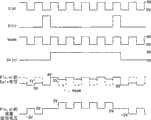
这里,在该现有的液晶显示装置中,TFT10变为截止状态后,通过改变对辅助电容线CsL(n)的施加电压,从而改变以(施加了一定电压Vcom的)公共电极为基准的像素电极的电位。参照图6和图7,详细说明这种电位的变化。Here, in this conventional liquid crystal display device, after the
图6是在现有的液晶显示装置中进行白显示时的各种信号的波形图,图7是在现有的液晶显示装置中进行黑显示时的各种信号的波形图。这些图6和图7所示的作为对视频信号线SL(m)施加的电压信号的视频信号S(m)实际上具有0V~4V之间的、与像素亮度对应的预定电压值,但为了便于说明,图6中视频信号S(m)的电压值为与白显示(最高亮度)对应的电压值,图7中视频信号S(m)的电压值为与黑显示(最低亮度)对应的电压值。通过使视频信号S(m)的最低电压为0V,可以简化电源电路的结构,并且可以抑制整体功耗。6 is a waveform diagram of various signals when a conventional liquid crystal display device performs white display, and FIG. 7 is a waveform diagram of various signals when a conventional liquid crystal display device performs black display. The video signal S(m) shown in these FIGS. 6 and 7 as a voltage signal applied to the video signal line SL(m) actually has a predetermined voltage value between 0V and 4V corresponding to the pixel brightness, but For convenience of explanation, the voltage value of the video signal S(m) in Fig. 6 corresponds to the voltage value corresponding to the white display (highest brightness), and the voltage value of the video signal S(m) in Fig. 7 corresponds to the voltage value corresponding to the black display (lowest brightness). Voltage value. By making the lowest voltage of the video signal S(m) 0V, the configuration of the power supply circuit can be simplified, and the overall power consumption can be suppressed.
这里,由于为了防止液晶层随时间发生劣化,需要进行交流驱动,因此在公共电极的电位Vcom固定时,很多情况下该公共电位Vcom设定为视频信号的(变化幅度的)中间电压。这样是由于可以使以公共电极的电位为基准的像素电极的电位实现交流化。这里,将公共电位Vcom设定为2V。Here, since AC driving is required to prevent the liquid crystal layer from deteriorating over time, when the potential Vcom of the common electrode is fixed, the common potential Vcom is often set to an intermediate voltage (variable range) of the video signal. This is because the potential of the pixel electrode can be made to alternate with the potential of the common electrode as a reference. Here, the common potential Vcom is set to 2V.
但是,在常黑型液晶显示装置中,为了使其液晶层的透射率为最大,通常需要至少4V左右的施加电压。因而,上述结构中对液晶的施加电压为±2V的范围,不能说很充分。还有,即使是在TN(扭曲向列)模式的常白型液晶显示装置中,由于对液晶施加的电压越大,则通过纯黑显示使得对比度越高,因此,±2V范围的施加电压也不能说很充分。However, in a normally black liquid crystal display device, in order to maximize the transmittance of the liquid crystal layer, an applied voltage of at least about 4 V is generally required. Therefore, it cannot be said that the voltage applied to the liquid crystal is in the range of ±2V in the above structure. Also, even in a normally white liquid crystal display device of the TN (twisted nematic) mode, since the larger the voltage applied to the liquid crystal, the higher the contrast ratio will be through pure black display, therefore, the applied voltage in the range of ±2V is also Can't say enough.
因此,在该现有的液晶显示装置中,通过驱动辅助电容线CsL(n)来改变像素电极的电位。即,由后文所述的图2所示的连接关系可知,像素电极Epix的电位在将公共电极Ecom作为基准时,相对于辅助电容线CsL(n)的电位变化,是根据辅助电容对液晶电容值Clc和辅助电容值Ccs之和的比例发生变化。例如,在图6所示的白显示的情况下,若提供给辅助电容线的信号(以下,将该信号称为“辅助电容线驱动信号”)Cs(n)的电位变化4V,则在液晶电容值Clc∶辅助电容值Ccs=1∶1时,即Ccs/(Ccs+Clc)=0.5时,像素电极Epix的电位变化2V。Therefore, in this conventional liquid crystal display device, the potential of the pixel electrode is changed by driving the storage capacitance line CsL(n). That is, as can be seen from the connection relationship shown in FIG. 2 described later, the potential of the pixel electrode Epix changes with respect to the potential of the storage capacitor line CsL(n) when the common electrode Ecom is taken as a reference, and is due to the effect of the storage capacitor on the liquid crystal. The ratio of the sum of the capacitance value Clc and the auxiliary capacitance value Ccs changes. For example, in the case of white display shown in FIG. 6, if the potential of the signal Cs(n) supplied to the storage capacitor line (hereinafter, this signal is referred to as "storage capacitor line drive signal") changes by 4V, the liquid crystal When capacitance value Clc: auxiliary capacitance value Ccs=1:1, that is, when Ccs/(Ccs+Clc)=0.5, the potential of the pixel electrode Epix changes by 2V.
因而,如图6所示,像素形成部P(n,m)的像素电极电位在扫描信号G(n)从(使TFT10导通的)激活状态变为非激活状态的时刻保持在4V,但由于之后辅助电容线驱动信号Cs(n)的上述电位变化而再上升2V,变为6V。因而,由于公共电位Vcom为2V,所以该时刻对液晶层的施加电压为4V。此外,这里忽略因扫描信号线的寄生电容而导致的电位变化。Therefore, as shown in FIG. 6 , the pixel electrode potential of the pixel forming portion P(n, m) is kept at 4V at the time when the scanning signal G(n) changes from the active state (which turns on the TFT 10 ) to the inactive state, but Due to the above-mentioned potential change of the auxiliary capacitance line drive signal Cs(n) thereafter, it further rises by 2V and becomes 6V. Therefore, since the common potential Vcom is 2V, the voltage applied to the liquid crystal layer at this time is 4V. In addition, the potential change due to the parasitic capacitance of the scanning signal line is ignored here.
这种电位变化是以白显示(最高亮度)进行像素显示的情况,但在以黑显示(最低亮度)进行像素显示的情况下,电位变化的形态相同,但其电位变化量不同。即,通常液晶具有介电常数各向异性,用于常黑型液晶显示装置的液晶的介电常数在进行白显示时比进行黑显示时要高,因而可知液晶电容值Clc更大。具体而言,对于上述那样在白显示的情况下Ccs/(Ccs+Clc)=0.5的液晶,在例如黑显示的情况下为Ccs/(Ccs+Clc)=0.75。Such a potential change is the same when a pixel is displayed in white display (highest luminance), but in the case of a pixel display in black display (lowest luminance), the form of potential change is the same, but the amount of potential change is different. That is, liquid crystals generally have dielectric anisotropy, and the dielectric constant of liquid crystals used in normally black liquid crystal display devices is higher when displaying white than when displaying black, so it can be seen that the liquid crystal capacitance Clc is larger. Specifically, for a liquid crystal having Ccs/(Ccs+Clc)=0.5 in the case of white display as described above, Ccs/(Ccs+Clc)=0.75 in the case of black display, for example.
因而,如图7所示,进行黑显示的像素形成部P(n,m)的像素电极电位在扫描信号G(n)变为非激活状态的时刻保持在0V,但由于之后辅助电容线驱动信号Cs(n)的(4V的)上述电位变化而上升3V,结果变为3V。因而,由于公共电位Vcom为2V,所以该时刻对液晶层的施加电压为1V。由于该电压值小于驱动液晶分子的液晶阈值电压值(通常为1.5V左右),所以液晶层的光透射率为0,对于黑显示来说是合适的值。上述动作对于极性反转的下一行的像素形成部P(n+1,m)的像素电极电位及下一帧的像素形成部P(n,m)也是一样的。这样既固定了公共电位Vcom、又驱动辅助电容线的液晶显示装置,在例如日本专利特开2001-83943号公报中已有揭示。以下,将该已有例称为第一已有例。Therefore, as shown in FIG. 7 , the pixel electrode potential of the pixel forming portion P(n, m) performing black display is kept at 0 V when the scanning signal G(n) becomes inactive, but due to the subsequent auxiliary capacitor line drive The above-mentioned potential (of 4V) of the signal Cs(n) changes and rises by 3V, resulting in 3V. Therefore, since the common potential Vcom is 2V, the voltage applied to the liquid crystal layer at this time is 1V. Since this voltage value is lower than the liquid crystal threshold voltage value (usually about 1.5V) for driving liquid crystal molecules, the light transmittance of the liquid crystal layer is 0, which is an appropriate value for black display. The above-described operation is the same for the pixel electrode potential of the pixel formation part P(n+1, m) in the next row whose polarity is reversed and the pixel formation part P(n, m) of the next frame. Such a liquid crystal display device in which the common potential Vcom is fixed and the auxiliary capacitor line is driven is disclosed in, for example, Japanese Patent Application Laid-Open No. 2001-83943. Hereinafter, this conventional example is referred to as a first conventional example.
另外,也有通过每隔一个扫描期间驱动公共电极Ecom来改变公共电位Vcom、以使其为与视频信号S(m)极性相反的电位(例如0V或4V)的现有液晶显示装置。若采用该现有结构,则可以使得对液晶的施加电压为±4V的范围。Also, there is a conventional liquid crystal display device that changes the common potential Vcom to a potential (for example, 0V or 4V) opposite in polarity to the video signal S(m) by driving the common electrode Ecom every other scanning period. According to this conventional structure, the voltage applied to the liquid crystal can be within the range of ±4V.
此外,在上述现有结构中,不一定需要驱动辅助电容线,但也有每隔一个扫描期间、与公共电极同相位地驱动辅助电容线的现有液晶显示装置。若采用该现有结构,则通过用适当的电位驱动辅助电容线,可以抑制闪烁或图像存储现象等。这种现有液晶显示装置在例如日本专利特开平2-913号公报等中已有揭示。以下,将该已有例称为第二已有例。In addition, in the above-mentioned conventional structure, it is not necessarily necessary to drive the storage capacitor line, but there is a conventional liquid crystal display device in which the storage capacitor line is driven in phase with the common electrode every other scanning period. According to this conventional structure, by driving the storage capacitor line with an appropriate potential, it is possible to suppress flicker, image memory, and the like. Such a conventional liquid crystal display device is disclosed in, for example, Japanese Patent Application Laid-Open No. 2-913. Hereinafter, this conventional example is referred to as a second conventional example.
专利文献1:日本专利特开2001-83943号公报Patent Document 1: Japanese Patent Laid-Open No. 2001-83943
专利文献2:日本专利特开平2-913号公报Patent Document 2: Japanese Patent Laid-Open No. 2-913
发明内容Contents of the invention
这里,上述第一已有例中对液晶的施加电压的绝对值在白显示时最大为4V,在黑显示时最小为1V,但由于如前所述在常黑型液晶显示装置中,为了使液晶层的透射率为100%,通常需要5V左右的施加电压,因此,上述现有液晶显示装置中,存在液晶施加电压的绝对值的最大值还差1V左右的问题。Here, the absolute value of the voltage applied to the liquid crystal in the above-mentioned first conventional example is at most 4V at the time of white display, and at least 1V at the time of black display. The transmittance of the liquid crystal layer is 100%, and an applied voltage of about 5V is usually required. Therefore, in the above-mentioned conventional liquid crystal display device, there is a problem that the maximum absolute value of the liquid crystal applied voltage is about 1V short.
因此,该第一已有例中,为了增加上述最大值,考虑采用增大辅助电容线驱动信号Cs(n)的电位最大值(即增大信号振幅)的结构。这里,若上述最大值为6V,则可以使液晶施加电压的绝对值的最大值为5V。然而,该结构使得辅助电容线驱动电路的制造成本升高,并且液晶施加电压的绝对值的最小值变为2.5V,在黑显示的情况下大大超过了液晶阈值电压值(通常为1.5V左右)。因而,即使是在黑显示的情况下,也由于以低亮度进行显示,因此使得对比度降低,从而导致显示装置的显示性能降低。这样,由于液晶施加电压的绝对值的最大值越大,则液晶施加电压的绝对值的最小值更大,所以使得该绝对值的最大值与最小值之差(即动态范围)变小,其结果,无法在0%~100%的范围内改变液晶的光透射率。Therefore, in this first conventional example, in order to increase the above-mentioned maximum value, it is conceivable to employ a configuration in which the potential maximum value of the storage capacitor line drive signal Cs(n) is increased (that is, the signal amplitude is increased). Here, if the above-mentioned maximum value is 6V, the maximum value of the absolute value of the liquid crystal application voltage can be set to 5V. However, this structure increases the manufacturing cost of the auxiliary capacitance line drive circuit, and the minimum value of the absolute value of the voltage applied to the liquid crystal becomes 2.5V, which greatly exceeds the liquid crystal threshold voltage value (usually about 1.5V) in the case of black display. ). Therefore, even in the case of black display, since the display is performed with low luminance, the contrast is lowered, and the display performance of the display device is lowered. Like this, since the maximum value of the absolute value of the voltage applied to the liquid crystal is larger, the minimum value of the absolute value of the voltage applied to the liquid crystal is larger, so the difference between the maximum value and the minimum value of the absolute value (that is, the dynamic range) becomes smaller, and its As a result, the light transmittance of the liquid crystal cannot be changed within the range of 0% to 100%.
此外,为了增加上述最大值,也考虑了采用增大辅助电容值的结构,但由于辅助电容值越大,则像素开口率越小,所以仍然会导致显示装置的显示性能降低。In addition, in order to increase the above-mentioned maximum value, it is also considered to adopt a structure of increasing the value of the auxiliary capacitor, but since the larger the value of the auxiliary capacitor, the smaller the aperture ratio of the pixel will be, so the display performance of the display device will still be reduced.
另外,在第二已有例中,若在0V~5V的范围内驱动公共电极及辅助电容线,则可以使液晶施加电压的绝对值的最大值为5V。然而,对于驱动公共电极及辅助电容线的驱动器电路的驱动电压范围(振幅),从容易进行其耐压设计和降低功耗等观点来看,以尽可能小为佳。In addition, in the second conventional example, if the common electrode and the auxiliary capacitor line are driven within the range of 0V to 5V, the maximum absolute value of the voltage applied to the liquid crystal can be set to 5V. However, the drive voltage range (amplitude) of the driver circuit for driving the common electrode and the auxiliary capacitor line should be as small as possible from the viewpoint of easy withstand voltage design and power consumption reduction.
因此,本发明的目的在于提供一种驱动辅助电容线的液晶显示装置,该液晶显示装置既可以将驱动电压的范围抑制得较小、又可以减小应对液晶施加的电压的绝对值的最大值与最小值之差那样来进行驱动。Therefore, an object of the present invention is to provide a liquid crystal display device for driving an auxiliary capacitor line, which can suppress the range of the driving voltage to a small range and reduce the maximum value of the absolute value of the voltage to be applied to the liquid crystal. Drive as the difference from the minimum value.
本发明的第一方面是有源矩阵型的液晶显示装置,该液晶显示装置的特征在于,包括:A first aspect of the present invention is an active matrix liquid crystal display device, which is characterized in that it includes:
驱动多根视频信号线的视频信号线驱动电路,该多根视频信号线用于传输与从装置外部提供的、用于显示预定图像的图像信号对应的多个视频信号;a video signal line driving circuit for driving a plurality of video signal lines for transmitting a plurality of video signals corresponding to image signals for displaying a predetermined image supplied from outside the device;
驱动多根扫描信号线的扫描信号线驱动电路,该多根扫描信号线与所述多根视频信号线交叉;a scanning signal line driving circuit for driving a plurality of scanning signal lines crossing the plurality of video signal lines;
驱动多根辅助电容线的辅助电容线驱动电路,该多根辅助电容线沿所述多根扫描信号线而对应配置;an auxiliary capacitor line driving circuit for driving a plurality of auxiliary capacitor lines, the plurality of auxiliary capacitor lines are correspondingly arranged along the plurality of scanning signal lines;
沿所述多根视频信号线和所述多根扫描信号线配置成矩阵状的多个像素形成部;以及a plurality of pixel forming portions arranged in a matrix along the plurality of video signal lines and the plurality of scanning signal lines; and
驱动公共电极的公共电极驱动电路,该公共电极对所述多个像素形成部提供公共电位,a common electrode drive circuit that drives a common electrode that supplies a common potential to the plurality of pixel forming portions,
所述多个像素形成部分别包含像素电极,该像素电极是与所述多根视频信号线中对应的视频信号线连接的电极,在与对应的辅助电容线之间形成预定的辅助电容,在与所述公共电极之间存在液晶,Each of the plurality of pixel forming parts includes a pixel electrode, which is an electrode connected to a corresponding video signal line among the plurality of video signal lines, and forms a predetermined storage capacitance with a corresponding storage capacitance line, and is connected to a corresponding storage capacitance line. and the liquid crystal exists between the common electrode,
所述扫描信号线驱动电路每次有选择地驱动所述多根扫描信号线中的一根时,或隔开驱动一根以上的间隔时,所述公共电极驱动电路对所述公共电极交替地施加预定的第一电位及大于该第一电位的第二电位中的任一个电位,使得以所述公共电极为基准的所述像素电极的极性反转,Each time when the scanning signal line driving circuit selectively drives one of the plurality of scanning signal lines, or at intervals of driving more than one scanning signal line, the common electrode driving circuit alternately drives the common electrodes. applying any one of a predetermined first potential and a second potential greater than the first potential, so that the polarity of the pixel electrode based on the common electrode is reversed,
所述辅助电容线驱动电路在对应的扫描信号线被所述扫描信号线驱动电路选择并从选择状态转移到非选择状态的第一时刻之后,施加预定的第三电位及大于该第三电位的第四电位中的任一个电位,使其与所述第一时刻或紧接所述第一时刻之后的所述公共电极的电位变化向同一方向变化,并且,在到所述对应的扫描信号线下一次被选择并从选择状态转移到非选择状态的第二时刻或所述第二时刻之前的附近时刻为止的预定期间内,驱动所述多根辅助电容线,使得维持所施加的电位。After the corresponding scanning signal line is selected by the scanning signal line driving circuit and shifts from the selected state to the non-selected state at the first moment, the auxiliary capacitor line driving circuit applies a predetermined third potential and a voltage higher than the third potential. Any one of the fourth potentials changes in the same direction as the potential change of the common electrode at or immediately after the first moment, and, when reaching the corresponding scanning signal line The plurality of storage capacitor lines are driven so as to maintain the applied potentials for a predetermined period until a second time when the selected state transitions from the selected state to the non-selected state next time or a time near the second time.
本发明的第二方面的特征在于,在本发明的第一方面中,A second aspect of the present invention is characterized in that, in the first aspect of the present invention,
作为所述视频信号最小值的第五电位、所述第一电位、和所述第三电位中的至少两个电位实质上一致。At least two of the fifth potential that is the minimum value of the video signal, the first potential, and the third potential substantially coincide.
本发明的第三方面的特征在于,在本发明的第二方面中,A third aspect of the present invention is characterized in that, in the second aspect of the present invention,
作为所述视频信号最小值的第五电位、所述第一电位、和所述第三电位中的至少两个电位为0V或0V附近的值。At least two of the fifth potential which is the minimum value of the video signal, the first potential, and the third potential are 0V or a value near 0V.
本发明的第四方面的特征在于,在本发明的第一方面中,A fourth aspect of the present invention is characterized in that, in the first aspect of the present invention,
作为所述视频信号最大值的第六电位、所述第二电位、和所述第四电位中的至少两个电位实质上一致。At least two of the sixth potential that is the maximum value of the video signal, the second potential, and the fourth potential substantially coincide.
本发明的第五方面的特征在于,在本发明的第四方面中,A fifth aspect of the present invention is characterized in that, in the fourth aspect of the present invention,
作为所述视频信号最大值的第六电位、所述第二电位、和所述第四电位中的至少两个电位为小于使所述液晶的光透射率在100%附近的施加电压的最小值的绝对值的值。At least two of the sixth potential, the second potential, and the fourth potential, which are the maximum value of the video signal, are smaller than a minimum value of an applied voltage that makes light transmittance of the liquid crystal near 100%. The absolute value of the value.
本发明的第六方面的特征在于,在本发明的第五方面中,A sixth aspect of the present invention is characterized in that, in the fifth aspect of the present invention,
作为所述视频信号最大值的第五电位、所述第二电位、和所述第四电位中的至少两个电位为4V或4V附近的值。At least two of the fifth potential that is the maximum value of the video signal, the second potential, and the fourth potential are 4V or a value near 4V.
本发明的第七方面是驱动液晶显示装置的方法,该液晶显示装置包括:用于传输与从装置外部提供的、用于显示预定图像的图像信号对应的多个视频信号的多根视频信号线;与所述多根视频信号线交叉的多根扫描信号线;沿所述多根扫描信号线对应配置的多根辅助电容线;提供公共电位的公共电极;以及沿所述多根视频信号线和所述多根扫描信号线配置成矩阵状的、包含像素电极的多个像素形成部,该像素电极是与所述多根视频信号线中的对应视频信号线连接的电极,在与对应的辅助电容线之间形成预定的辅助电容,在与所述公共电极之间存在液晶,该驱动方法的特征在于,包括:A seventh aspect of the present invention is a method of driving a liquid crystal display device including: a plurality of video signal lines for transmitting a plurality of video signals corresponding to an image signal for displaying a predetermined image supplied from outside the device ; a plurality of scanning signal lines crossing the plurality of video signal lines; a plurality of auxiliary capacitance lines correspondingly arranged along the plurality of scanning signal lines; a common electrode providing a common potential; and along the plurality of video signal lines a plurality of pixel forming portions arranged in a matrix with the plurality of scanning signal lines, including pixel electrodes, which are electrodes connected to corresponding video signal lines among the plurality of video signal lines; A predetermined auxiliary capacitor is formed between the auxiliary capacitor lines, and there is a liquid crystal between the common electrode and the common electrode. The driving method is characterized in that it includes:
驱动所述多根视频信号线的视频信号线驱动步骤;a video signal line driving step for driving the plurality of video signal lines;
驱动所述多根扫描信号线的扫描信号线驱动步骤;a scanning signal line driving step of driving the plurality of scanning signal lines;
驱动所述多根辅助电容线的辅助电容线驱动步骤;以及an auxiliary capacitor line driving step of driving the plurality of auxiliary capacitor lines; and
驱动所述公共电极的公共电极驱动步骤,a common electrode driving step of driving the common electrode,
在所述公共电极驱动步骤中,每次在所述扫描信号线驱动步骤中有选择地驱动所述多根扫描信号线中的一根时,或隔开驱动一根以上的间隔时,对所述公共电极交替地施加预定的第一电位及大于该第一电位的第二电位中的任一个电位,使得以所述公共电极为基准的所述像素电极的极性反转,In the common electrode driving step, each time one of the plurality of scanning signal lines is selectively driven in the scanning signal line driving step, or when more than one scanning signal line is driven at intervals, all The common electrode is alternately applied with any one of a predetermined first potential and a second potential greater than the first potential, so that the polarity of the pixel electrode based on the common electrode is reversed,
在所述辅助电容线驱动步骤中,在对应的扫描信号线被在所述扫描信号线驱动步骤中选择并从选择状态转移到非选择状态的第一时刻之后,施加预定的第三电位及大于该第三电位的第四电位中的任一个电位,使其与所述第一时刻或紧接所述第一时刻之后的所述公共电极的电位变化向同一方向变化,并且,在到所述对应的扫描信号线下一次被选择并从选择状态转移到非选择状态的第二时刻或所述第二时刻之前的附近时刻为止的预定期间内,驱动所述多根辅助电容线,使得维持所施加的电位。In the auxiliary capacitance line driving step, after the first moment when the corresponding scanning signal line is selected in the scanning signal line driving step and shifts from the selected state to the non-selected state, a predetermined third potential greater than or equal to Any one of the third potential and the fourth potential changes in the same direction as the potential change of the common electrode at or immediately after the first moment, and, until the During the predetermined period until the second time when the corresponding scanning signal line is selected next time and transitions from the selected state to the non-selected state or a time near the second time, the plurality of auxiliary capacitor lines are driven so that all the storage capacitor lines are maintained. applied potential.
若采用本发明的第一方面,则采用如下结构来驱动多根辅助电容线:即,从第一时刻开始,施加第三电位或第四电位,使得与第一时刻的公共电极的电位变化向同一方向变化,在到第二时刻或该时刻之前的附近时刻为止的预定期间内保持所施加的电位,从而可以将驱动电压的范围抑制得较小,容易进行驱动电路的耐压设计,并且通过利用液晶对施加电压的介电常数各向异性,可以增大应对液晶施加的电压的绝对值的最大值与最小值之差那样来进行驱动。If the first aspect of the present invention is adopted, the following structure is adopted to drive a plurality of auxiliary capacitor lines: that is, from the first moment, the third potential or the fourth potential is applied so that the potential change of the common electrode at the first moment is in the same direction as Change in the same direction, and maintain the applied potential during the predetermined period until the second time or the time near the time, so that the range of the driving voltage can be suppressed to be small, and the withstand voltage design of the driving circuit is easy to carry out, and by Utilizing the dielectric constant anisotropy of the liquid crystal to the applied voltage, it is possible to drive so as to increase the difference between the maximum value and the minimum value of the absolute value of the voltage to be applied to the liquid crystal.
若采用本发明的第二方面,则使得第五电位、第一电位和第三电位中的至少两个电位实质上一致,从而由于不需要在电源电路中生成多种电位,因此,可以简化电源电路的结构。If the second aspect of the present invention is adopted, at least two potentials of the fifth potential, the first potential and the third potential are substantially identical, so that it is not necessary to generate multiple potentials in the power supply circuit, therefore, the power supply can be simplified. The structure of the circuit.
若采用本发明的第三方面,则由于第五电位、第一电位和第三电位中的至少两个电位为0V或0V附近的值,因此,可以抑制整体功耗。According to the third aspect of the present invention, since at least two of the fifth potential, the first potential, and the third potential are at or near 0 V, overall power consumption can be suppressed.
若采用本发明的第四方面,则使得第六电位、第二电位和第四电位中的至少两个电位实质上一致,从而由于不需要在电源电路中生成多种电位,因此,可以简化电源电路的结构。If the fourth aspect of the present invention is adopted, at least two of the sixth potential, the second potential, and the fourth potential are substantially the same, so that it is not necessary to generate multiple potentials in the power supply circuit, so the power supply can be simplified. The structure of the circuit.
若采用本发明的第五方面,则由于第六电位、第二电位和第四电位中的至少两个电位为小于使所述液晶的光透射率在100%附近的施加电压的最小值的绝对值的值,因此可以容易进行驱动电压的耐压设计,还可以抑制整体功耗。If the fifth aspect of the present invention is adopted, since at least two of the sixth potential, the second potential, and the fourth potential are absolute values smaller than the minimum value of the applied voltage that makes the light transmittance of the liquid crystal near 100%, Therefore, the withstand voltage design of the driving voltage can be easily performed, and the overall power consumption can be suppressed.
若采用本发明的第六方面,则由于第六电位、第二电位和第四电位中的至少两个电位为4V或4V附近的值,因此,通过使用通用的驱动电路,能特别容易进行耐压设计,还可以抑制整体功耗。According to the sixth aspect of the present invention, since at least two potentials of the sixth potential, the second potential and the fourth potential are at or near 4V, it is particularly easy to perform resistance by using a general-purpose drive circuit. The voltage design can also suppress the overall power consumption.
若采用本发明的第七方面,则在液晶显示装置的驱动方法中可以起到与本发明的第一方面同样的效果。According to the seventh aspect of the present invention, the same effect as that of the first aspect of the present invention can be achieved in the method of driving a liquid crystal display device.
附图说明Description of drawings
图1是表示本发明的一个实施方式的液晶显示装置的整体结构的框图。FIG. 1 is a block diagram showing the overall configuration of a liquid crystal display device according to one embodiment of the present invention.
图2是表示上述实施方式中的像素形成部的等效电路的电路图。FIG. 2 is a circuit diagram showing an equivalent circuit of a pixel forming portion in the above embodiment.
图3是表示上述实施方式中进行白显示时的各种信号等的波形图。FIG. 3 is a waveform diagram showing various signals and the like when white display is performed in the above-described embodiment.
图4是表示上述实施方式中进行黑显示时的各种信号等的波形图。FIG. 4 is a waveform diagram showing various signals and the like when black display is performed in the above embodiment.
图5是表示上述实施方式中对液晶层的施加电压与其光透射率的关系的图。FIG. 5 is a graph showing the relationship between the voltage applied to the liquid crystal layer and its light transmittance in the above embodiment.
图6是表示现有液晶显示装置中进行白显示时的各种信号等的波形图。6 is a waveform diagram showing various signals and the like when a white display is performed in a conventional liquid crystal display device.
图7是表示现有液晶显示装置中进行黑显示时的各种信号等的波形图。7 is a waveform diagram showing various signals and the like when black display is performed in a conventional liquid crystal display device.
标号说明Label description
10TFT(开关元件)10TFT (switching element)
200显示控制电路200 display control circuit
300源极驱动器300 source drivers
400栅极驱动器400 gate driver
500辅助电容线驱动电路500 Auxiliary Capacitor Line Driver Circuit
600公共电极驱动部600 common electrode driver
700显示部700 display unit
Ecom公共电极Ecom common electrode
Vcom公共电位Vcom common potential
Epix像素电极Epix pixel electrodes
GL(n)扫描信号线(n=1~N)GL(n) scan signal line (n=1~N)
G(n)扫描信号(n=1~N)G(n) scanning signal (n=1~N)
CsL(n)辅助电容线(n=1~N)CsL(n) auxiliary capacitor line (n=1~N)
Cs(n)辅助电容线驱动信号(n=1~N)Cs(n) auxiliary capacitor line drive signal (n=1~N)
SL(m)视频信号线(m=1~M)SL(m) video signal line (m=1~M)
S(m)视频信号(m=1~M)S(m) video signal (m=1~M)
P(n,m)像素形成部(n=1~N,m=1~M)P(n, m) pixel formation part (n=1 to N, m=1 to M)
具体实施方式Detailed ways
下面,参照附图说明本发明的各实施方式。在以下的说明中,显示部采用垂直取向方式的常黑的结构,作为驱动方式,采用对像素形成部的液晶部分施加的电压每隔相邻一行相互为反极性、且每隔一帧为反极性的所谓行反转驱动方式此外,也可以采用每隔两行以上相互为反极性的所谓n行反转驱动方式。Hereinafter, various embodiments of the present invention will be described with reference to the drawings. In the following description, the display part adopts a vertically aligned normally black structure, and as a driving method, the voltages applied to the liquid crystal part of the pixel forming part are opposite to each other every other adjacent row, and every other frame is So-called row inversion driving method of inverse polarity Alternatively, a so-called n-row inversion driving method in which polarities are reversed for every two or more rows may be employed.
<1.液晶显示装置的整体结构及动作><1. Overall structure and operation of liquid crystal display device>
图1是表示本发明的一个实施方式的有源矩阵型的液晶显示装置的整体结构的框图。该液晶显示装置包括:由显示控制电路200、源极驱动器(视频信号线驱动电路)300、栅极驱动器(扫描信号线驱动电路)400、辅助电容线驱动电路500、和公共电极驱动电路600构成的驱动控制部;以及显示部700。FIG. 1 is a block diagram showing the overall configuration of an active matrix liquid crystal display device according to one embodiment of the present invention. The liquid crystal display device includes: a display control circuit 200, a source driver (video signal line drive circuit) 300, a gate driver (scanning signal line drive circuit) 400, an auxiliary capacitance line drive circuit 500, and a common electrode drive circuit 600. The drive control part; and the display part 700.
显示部700包括:多根(M根)视频信号线SL(1)~SL(M);多根(N根)扫描信号线GL(1)~GL(N)和辅助电容线CsL(1)~CsL(N);以及沿这些多根视频信号线SL(1)~SL(M)和多根扫描信号线GL(1)~GL(N)设置的多个(M×N个)像素形成部。以下,与扫描信号线GL(n)和视频信号线SL(m)的交叉点相关联地用参考标号“P(n,m)”表示设置于该交叉点附近(图中为该交叉点的右下附近)的像素形成部。图2是表示本实施方式的显示部700中的像素形成部P(n,m)的等效电路。The display unit 700 includes: a plurality (M) of video signal lines SL(1) to SL(M); a plurality of (N) scanning signal lines GL(1) to GL(N) and a storage capacitor line CsL(1) ~CsL(N); and a plurality of (M×N) pixels arranged along these multiple video signal lines SL(1)~SL(M) and multiple scanning signal lines GL(1)~GL(N) are formed department. Hereinafter, in association with the intersection of the scanning signal line GL(n) and the video signal line SL(m), reference numerals "P(n, m)" are used to denote those disposed in the vicinity of the intersection (the intersection of the intersection in the figure). Near the bottom right) of the pixel forming part. FIG. 2 shows an equivalent circuit of the pixel formation portion P(n, m) in the display portion 700 of the present embodiment.
如图2所示,各像素形成部P(n,m)由以下构成:栅极端子与扫描信号线GL(n)或与其相邻的扫描信号线GL(n+1)连接、且源极端子与通过相应交叉点的视频信号线SL(m)或与其相邻的视频信号线SL(m+1)连接的开关元件即TFT10;与该TFT10的漏极端子连接的像素电极Epix;对上述多个像素形成部P(i,j)(i=1~N,j=1~M)共同设置的公共电极Ecom;以及在对上述多个像素形成部P(i,j)(i=1~N,j=1~M)共同设置的像素电极Epix与公共电极Ecom之间夹着的作为电光学元件的液晶层。As shown in FIG. 2 , each pixel forming portion P(n, m) is composed of a gate terminal connected to a scanning signal line GL(n) or a scanning signal line GL(n+1) adjacent thereto, and a source terminal A switch element that is connected to the video signal line SL (m) passing through the corresponding cross point or the video signal line SL (m+1) adjacent to it is the TFT10; the pixel electrode Epix connected to the drain terminal of the TFT10; A common electrode Ecom provided jointly by a plurality of pixel formation parts P(i, j) (i=1~N, j=1~M); ˜N, j=1˜M) A liquid crystal layer as an electro-optical element sandwiched between the common electrode Epix and the common electrode Ecom.
此外,各像素形成部P(n,m)显示红色(R)、绿色(G)、和蓝色(B)中的某一种颜色,如图2所示,显示同一颜色的像素形成部P(n,m)沿视频信号线SL(1)~SL(M)配置,且在沿扫描信号线GL(1)~GL(N)的方向上按照RGB的顺序配置。In addition, each pixel forming portion P(n, m) displays one of red (R), green (G), and blue (B), and as shown in FIG. 2 , the pixel forming portion P of the same color displays (n, m) are arranged along the video signal lines SL( 1 ) to SL(M), and are arranged in the order of RGB in the direction along the scanning signal lines GL( 1 ) to GL(N).
在各像素形成部P(n,m)中,由像素电极Epix、和与之夹着液晶层而相对的公共电极Ecom形成液晶电容(也称为像素电容)Clc。对各像素电极Epix设置两根视频信号线SL(m)、SL(m+1),使其夹着该像素电极,视频信号线SL(m)通过TFT10与该像素电极Epix连接。In each pixel forming portion P(n, m), a liquid crystal capacitance (also referred to as a pixel capacitance) Clc is formed by the pixel electrode Epix and the common electrode Ecom opposed thereto with the liquid crystal layer interposed therebetween. Two video signal lines SL(m) and SL(m+1) are provided for each pixel electrode Epix so as to sandwich the pixel electrode, and the video signal line SL(m) is connected to the pixel electrode Epix through a TFT10.
另外,与各扫描信号线GL(n)平行地形成辅助电容线CsL(n),在各像素形成部P(n,m)中,在像素电极Epix和辅助电容线CsL(n)之间形成辅助电容Ccs。In addition, a storage capacitor line CsL(n) is formed parallel to each scanning signal line GL(n), and in each pixel formation portion P(n, m), is formed between the pixel electrode Epix and the storage capacitor line CsL(n). Auxiliary capacitor Ccs.
显示控制电路200接受从外部发送来的显示数据信号DAT和定时控制信号TS,输出数字图像信号DV、用于控制在显示部700显示图像的定时的源极起始脉冲信号SSP、源极时钟信号SCK、锁存选通信号LS、栅极起始脉冲信号GSP、栅极时钟信号GCK、辅助电容线控制信号Scs、以及公共电极控制信号Sec。The display control circuit 200 receives a display data signal DAT and a timing control signal TS sent from the outside, and outputs a digital image signal DV, a source start pulse signal SSP and a source clock signal for controlling the timing of displaying an image on the display unit 700 SCK, a latch strobe signal LS, a gate start pulse signal GSP, a gate clock signal GCK, an auxiliary capacitance line control signal Scs, and a common electrode control signal Sec.
源极驱动器300接受从显示控制电路200输出的数字图像信号DV、源极起始脉冲信号SSP、源极时钟信号SCK、以及锁存选通信号LS,对各视频信号线SL(1)~SL(M)施加驱动用视频信号S(1)~S(M),用于对显示部700内的各像素形成部P(n,m)的液晶电容Clc进行充电。这时,源极驱动器300中,在源极时钟信号SCK的脉冲发生的定时,依次保持表示应对各视频信号线SL(1)~SL(M)施加的电压的数字图像信号DV。然后,在锁存选通信号LS的脉冲发生的定时,将上述所保持的数字图像信号DV转换成模拟电压。The source driver 300 receives the digital video signal DV output from the display control circuit 200, the source start pulse signal SSP, the source clock signal SCK, and the latch strobe signal LS, and transmits the signal to each video signal line SL(1)˜SL. (M) Apply driving video signals S( 1 ) to S(M) for charging the liquid crystal capacitance Clc of each pixel forming part P(n, m) in the display part 700 . At this time, source driver 300 sequentially holds digital video signal DV indicating voltages to be applied to video signal lines SL( 1 ) to SL(M) at the timing of pulse generation of source clock signal SCK. Then, at the timing when the pulse of the latch strobe signal LS is generated, the above-mentioned held digital image signal DV is converted into an analog voltage.
这种D/A转换是通过源极驱动器300中包含的D/A转换电路(及灰度电压生成电路)进行的。该D/A转换电路通过对例如从源极驱动器300的外部提供的、用于生成灰度电压的基准电压进行分压,从而生成与各显示灰度对应的模拟电压。通过该D/A转换电路生成的模拟电压作为驱动用视频信号,一齐施加到所有视频信号线SL(1)~SL(M)上。即,本实施方式中,视频信号线SL(1)~SL(M)的驱动方式采用线顺序驱动方式。Such D/A conversion is performed by a D/A conversion circuit (and a gradation voltage generating circuit) included in the source driver 300 . This D/A conversion circuit generates analog voltages corresponding to respective display gradations by dividing a reference voltage for generating gradation voltages supplied from outside the source driver 300 , for example. The analog voltage generated by this D/A conversion circuit is applied collectively to all video signal lines SL( 1 ) to SL(M) as a video signal for driving. That is, in this embodiment, the driving method of the video signal lines SL( 1 ) to SL(M) adopts the line sequential driving method.
栅极驱动器400根据从显示控制电路200输出的栅极起始脉冲信号GSP和栅极时钟信号GCK,对各扫描信号线GL(1)~GL(N)依次施加激活的扫描信号G(1)~G(N)。The gate driver 400 sequentially applies the active scanning signal G(1) to the scanning signal lines GL(1)˜GL(N) according to the gate start pulse signal GSP and the gate clock signal GCK output from the display control circuit 200 ~G(N).
辅助电容线驱动电路500根据从显示控制电路200输出的辅助电容线控制信号Scs,对各辅助电容线CsL(1)~CsL(N)依次施加基于从未图示的电源电路提供的电位的、电位呈两段变化的辅助电容线驱动信号Cs(1)~Cs(N)。该辅助电容线控制信号Scs包括:与例如栅极起始脉冲信号GSP及栅极时钟信号SCK相当的起始脉冲信号及时钟信号;以及表示极性反转(或上述电位选择)的定时的信号。The storage capacitor line drive circuit 500 sequentially applies, to the respective storage capacitor lines CsL( 1 ) to CsL(N) based on potentials supplied from a power supply circuit not shown, based on the storage capacitor line control signal Scs output from the display control circuit 200 . Auxiliary capacitance line drive signals Cs(1)˜Cs(N) whose potentials change in two stages. The auxiliary capacitance line control signal Scs includes: a start pulse signal and a clock signal corresponding to, for example, the gate start pulse signal GSP and the gate clock signal SCK; and a signal indicating the timing of polarity inversion (or the above-mentioned potential selection) .
公共电极驱动电路600根据从显示控制电路200输出的公共电极线控制信号Sec,对公共电极施加基于从未图示的电源电路提供的电位的、呈两段变化的电位,使得应对液晶施加的电压的极性根据视频信号S(m)的变化而反转。该公共电极控制信号Sec包括:与例如源极时钟信号SCK相当的时钟信号;以及表示极性反转(或上述电位选择)的定时的信号。The common electrode drive circuit 600 applies a potential that changes in two steps based on a potential supplied from a power supply circuit not shown to the common electrode based on the common electrode line control signal Sec output from the display control circuit 200 so as to respond to the voltage applied to the liquid crystal. The polarity of is reversed according to the change of the video signal S(m). The common electrode control signal Sec includes: a clock signal corresponding to, for example, the source clock signal SCK; and a signal indicating the timing of polarity inversion (or the aforementioned potential selection).
这里,从图2所示的连接关系可知,若对这些辅助电容线CsL(1)~CsL(N)施加的电压发生变化,则像素电极Epix的电位在将公共电极Ecom作为基准时,相对于辅助电容线CsL(n)的电位变化,根据辅助电容对液晶电容值和辅助电容值之和的比例发生变化。由此,可以使公共电位Vcom与各像素形成部中的像素电极的电位差在白显示的情况下增大(换言之,提高像素电极的电压)。该信号的波形等将在后文中阐述。Here, as can be seen from the connection relationship shown in FIG. 2 , when the voltages applied to these storage capacitor lines CsL(1) to CsL(N) change, the potential of the pixel electrode Epix will be relative to the common electrode Ecom as a reference. The potential change of the storage capacitance line CsL(n) changes according to the ratio of the storage capacitance to the sum of the liquid crystal capacitance value and the storage capacitance value. This makes it possible to increase the potential difference between the common potential Vcom and the pixel electrode in each pixel formation portion (in other words, increase the voltage of the pixel electrode) in the case of white display. The waveform and the like of this signal will be described later.
如上所述,通过对各视频信号线SL(1)~SL(M)施加驱动用视频信号、对各扫描信号线GL(1)~GL(N)施加扫描信号、对各辅助电容线CsL(1)~CsL(N)施加辅助电容线驱动信号,从而在显示部700上显示图像。接着,参照图3和图4,说明各种信号等的电位变化。As described above, by applying a driving video signal to each video signal line SL(1) to SL(M), and applying a scanning signal to each scanning signal line GL(1) to GL(N), each storage capacitor line CsL( 1) to CsL(N) apply a storage capacitor line drive signal to display an image on the display unit 700 . Next, potential changes of various signals and the like will be described with reference to FIGS. 3 and 4 .
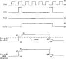
<2.各种信号等的波形><2. Waveforms of various signals, etc.>
图3是表示本液晶显示装置中进行白显示时的各种信号等的波形图。图4是表示本液晶显示装置中进行黑显示时的各种信号等的波形图。如图3和图4所示,对视频信号线SL(m)施加的电压信号即视频信号S(m)为0V~4V之间的与像素亮度对应的预定电压值,即在正极性的情况下,与黑显示(最低亮度)对应的电压值为0V,与白显示(最高亮度)对应的电压值为4V;在负极性的情况下,与黑显示(最低亮度)对应的电压值为4V,与白显示(最高亮度)对应的电压值为0V,具有±4V范围的电压值。通过使视频信号S(m)中的最低电压为0V,可以抑制整体功耗。FIG. 3 is a waveform diagram showing various signals and the like when white display is performed in the liquid crystal display device. FIG. 4 is a waveform diagram showing various signals and the like when black display is performed in the present liquid crystal display device. As shown in Figures 3 and 4, the voltage signal applied to the video signal line SL (m), that is, the video signal S (m), is a predetermined voltage value corresponding to the brightness of the pixel between 0V and 4V, that is, in the case of positive polarity In the case of negative polarity, the voltage value corresponding to black display (lowest brightness) is 0V, and the voltage value corresponding to white display (highest brightness) is 4V; in the case of negative polarity, the voltage value corresponding to black display (lowest brightness) is 4V , the voltage value corresponding to white display (highest brightness) is 0V, and has a voltage value in the range of ±4V. By making the lowest voltage in the video signal S(m) 0V, the overall power consumption can be suppressed.
另外,如前所述,由于为了防止液晶层随时间发生劣化,需要进行交流驱动,因此,公共电极Ecom的电位即公共电位Vcom作如下变化,即在正极性的情况下为0V,在负极性的情况下为4V,从而使得液晶施加电压的极性根据视频信号S(m)的变化而反转。因而例如,在始终进行白显示的情况下,相对于视频信号S(m)的变化,公共电位Vcom以相同的振幅、相反的相位进行变化In addition, as mentioned above, in order to prevent the deterioration of the liquid crystal layer over time, AC driving is required, so the potential of the common electrode Ecom, that is, the common potential Vcom, changes as follows, that is, it is 0 V in the case of positive polarity, and 0 V in the case of negative polarity. In the case of , it is 4V, so that the polarity of the voltage applied to the liquid crystal is reversed according to the change of the video signal S(m). Therefore, for example, in the case of always displaying white, the common potential Vcom changes with the same amplitude and opposite phase with respect to the change of the video signal S(m).
这里,由于为了使常黑型液晶显示装置中其液晶层的透射率为最大,通常需要5V左右(这里最大为5V)的施加电压,所以,通过与上述第一已有例中的液晶显示装置同样地驱动辅助电容线CsL(n),从而使像素电极的电位发生变化。即,像素电极Epix的电位在将公共电极Ecom作为基准时,相对于辅助电容线CsL(n)的电位变化,根据辅助电容对液晶电容值和辅助电容值之和的比例发生变化。Here, since in order to maximize the transmittance of the liquid crystal layer in a normally black liquid crystal display device, an applied voltage of about 5V (here, a maximum of 5V) is usually required, so by comparing with the liquid crystal display device in the above-mentioned first conventional example, Similarly, the storage capacitor line CsL(n) is driven to change the potential of the pixel electrode. That is, the potential of the pixel electrode Epix changes with respect to the potential change of the storage capacitor line CsL(n) with reference to the common electrode Ecom, according to the ratio of the storage capacitor to the sum of the liquid crystal capacitance and the storage capacitor.
例如,在图3所示的白显示的情况下,假设公共电位Vcom不发生变化,只有提供给辅助电容线的信号(以下,将该信号称为“辅助电容线驱动信号”)Cs(n)的电位变化4V,则在设液晶电容值Clc∶辅助电容值Ccs=1∶1即Ccs/(Ccs+Clc)=0.5时,像素电极Epix的电位变化2V。上述比率是白显示时的值,在进行黑显示时,由于如前所述液晶的介电常数变小,因此这里设Ccs/(Ccs+Clc)=0.75。黑显示的情况将参照图4在后文中阐述。For example, in the case of white display shown in FIG. 3 , assuming that the common potential Vcom does not change, only the signal supplied to the storage capacitor line (hereinafter, this signal will be referred to as "storage capacitor line drive signal") Cs(n) If the potential of the pixel electrode Epix changes by 4V, the potential of the pixel electrode Epix changes by 2V when the liquid crystal capacitance value Clc: auxiliary capacitance value Ccs=1:1, that is, Ccs/(Ccs+Clc)=0.5. The above-mentioned ratio is a value at the time of white display, and at the time of black display, since the dielectric constant of the liquid crystal decreases as described above, Ccs/(Ccs+Clc)=0.75 is set here. The case of black display will be described later with reference to FIG. 4 .
相反地,当假设辅助电容线驱动信号Cs(n)的电位不发生变化,只有公共电位Vcom变化4V时,由于Ccs/(Ccs+Clc)=0.5,所以像素电极Epix的电位变化2V。Conversely, assuming that the potential of the auxiliary capacitance line drive signal Cs(n) does not change and only the common potential Vcom changes by 4V, since Ccs/(Ccs+Clc)=0.5, the potential of the pixel electrode Epix changes by 2V.
当然,在辅助电容线驱动信号Cs(n)及公共电位Vcom的电位都变化4V的情况下,像素电极Epix的电位也相同地变化4V。即,液晶施加电压保持原样不变。Of course, when the potentials of the auxiliary capacitor line drive signal Cs(n) and the common potential Vcom both change by 4V, the potential of the pixel electrode Epix also changes by 4V in the same way. That is, the liquid crystal application voltage remains unchanged.
此外,该辅助电容线驱动信号Cs(n)是根据辅助电容线控制信号Scs,由辅助电容线驱动电路500生成,使其在与扫描信号G(n)下降的同一定时,沿与公共电极Vcom的电位变化的同一方向下降或上升。具体而言,如图3所示,在与扫描信号G(n)下降的同一定时下降后,在下一帧中的扫描信号G(n)下降的定时上升。更严密地说,辅助电容线驱动信号Cs(n)在TFT10完全变为截止状态的时刻、即比扫描信号G(n)的下降稍迟的定时下降后,在比下一帧中的扫描信号G(n)的下降稍迟的定时上升。这种情况对于公共电位Vcom的电位变化的定时也是同样的。In addition, the auxiliary capacitance line driving signal Cs(n) is generated by the auxiliary capacitance line driving circuit 500 according to the auxiliary capacitance line control signal Scs so that it is driven along the common electrode Vcom at the same timing as the scanning signal G(n) falls. Falling or rising in the same direction as the potential change. Specifically, as shown in FIG. 3 , after falling at the same timing as the falling of the scanning signal G(n), the timing of falling of the scanning signal G(n) in the next frame rises. More precisely, after the auxiliary capacitor line drive signal Cs(n) falls at the time when the
另外,如图3所示,像素形成部P(n,m)的像素电极电位到扫描信号G(n)从(使TFT10导通的)激活状态变为非激活状态的时刻为止都保持在4V,但由于之后公共电位Vcom及辅助电容线驱动信号Cs(n)的变化都是上升4V,所以再上升4V,变为8V。因而,由于公共电位Vcom为4V,所以该时刻对液晶层的施加电压保持原样为4V。In addition, as shown in FIG. 3 , the pixel electrode potential of the pixel forming portion P(n, m) is kept at 4V until the scanning signal G(n) changes from the active state (turning on the TFT 10 ) to the inactive state. , but since the changes of the common potential Vcom and the auxiliary capacitor line drive signal Cs(n) are both increased by 4V, they are increased by another 4V to become 8V. Therefore, since the common potential Vcom is 4V, the voltage applied to the liquid crystal layer at this time is 4V as it is.
这里,通常例如上述第二已有例那样,直到下一帧的显示时刻为止都保持该液晶施加电压,从而以与上述施加电压对应的亮度进行像素显示。即,没有辅助电容线的现有液晶显示装置便是如此,即使如第二已有例那样存在辅助电容线的情况,在使其电位与公共电位同时作同样变动的情况下,液晶施加电压也是从施加时刻开始都不发生变动,保持原样不变。Here, as in the above-mentioned second prior art example, normally, the liquid crystal application voltage is maintained until the display timing of the next frame, and pixel display is performed with a luminance corresponding to the above-mentioned applied voltage. That is, in the case of a conventional liquid crystal display device without an auxiliary capacitor line, even if there is an auxiliary capacitor line as in the second conventional example, the voltage applied to the liquid crystal will be the same if the potential of the same changes at the same time as the common potential. It does not change from the moment it is applied, and remains unchanged.
然而,本实施方式的很大的特征在于,根据之后的公共电位Vcom的变化而改变像素形成部P(n,m)的像素电极电位。即,如图3所示,若辅助电容线驱动信号Cs(n)的电位保持4V不发生变化,只有公共电位Vcom下降4V,则当Ccs/(Ccs+Clc)=0.5时,像素电极Epix的电位从8V下降2V,变为6V。其结果,液晶施加电压从4V上升到6V。这样,通过使液晶施加电压上升,可以使液晶施加电压的绝对值的最大值大于对公共电位进行反转驱动的现有液晶显示装置(例如上述第二已有例)中的驱动电压的最大值。However, a significant feature of the present embodiment is that the potential of the pixel electrode of the pixel formation portion P(n, m) is changed according to the subsequent change of the common potential Vcom. That is, as shown in FIG. 3, if the potential of the auxiliary capacitor line drive signal Cs(n) remains unchanged at 4V, and only the common potential Vcom drops by 4V, then when Ccs/(Ccs+Clc)=0.5, the pixel electrode Epix The potential drops 2V from 8V to 6V. As a result, the voltage applied to the liquid crystal rose from 4V to 6V. Thus, by increasing the voltage applied to liquid crystal, the maximum value of the absolute value of the voltage applied to liquid crystal can be made larger than the maximum value of the driving voltage in a conventional liquid crystal display device (for example, the above-mentioned second conventional example) that reversely drives the common potential. .
然后,辅助电容线驱动信号Cs(n)的电位不发生变化(维持原样不变),只有公共电位Vcom上升4V时,像素电极Epix的电位上升2V,变为8V,液晶施加电压变为4V。Then, the potential of the auxiliary capacitor line drive signal Cs(n) does not change (remains unchanged), and only when the common potential Vcom rises by 4V, the potential of the pixel electrode Epix rises by 2V to 8V, and the liquid crystal application voltage becomes 4V.
这样,通过维持辅助电容线的电位不变来驱动公共电极,使得液晶施加电压到下一帧的显示时刻为止,每隔一个扫描期间交替地变为4V或6V。然而,该变化并不反映于显示,显示状态不发生变化。这是由于,通常的液晶显示装置中一个扫描期间的长度为数十微秒~一百几十微秒左右,而一般液晶分子的取向状态变化需要十毫秒左右。因此,液晶分子的取向状态取决于其施加电压的有效值(平均值)。因而,如上所述,当液晶施加电压每隔一个扫描期间交替地变为4V或6V时,可以视为与始终对液晶施加5V的固定电压的情况相同。从而,在这种情况下,液晶层的光透射率始终为100%,可以稳定地进行白显示。In this way, by keeping the potential of the auxiliary capacitor line constant and driving the common electrode, the voltage applied to the liquid crystal is alternately changed to 4V or 6V every scanning period until the display timing of the next frame. However, this change is not reflected in the display, and the display state does not change. This is because the length of one scan period in a typical liquid crystal display device is about tens of microseconds to one hundred and tens of microseconds, and it usually takes about ten milliseconds for the alignment state of liquid crystal molecules to change. Therefore, the alignment state of the liquid crystal molecules depends on the effective value (average value) of the applied voltage. Therefore, as described above, when the liquid crystal application voltage is alternately changed to 4V or 6V every scanning period, it can be regarded as the same as the case where a fixed voltage of 5V is always applied to the liquid crystal. Therefore, in this case, the light transmittance of the liquid crystal layer is always 100%, and white display can be performed stably.
在始终进行白显示的情况下,如上述图3所示那样动作,因此,接下来参照图4说明始终进行黑显示的例子。如图4所示,像素形成部P(n,m)的像素电极电位到扫描信号G(n)从(使TFT10导通的)激活状态变为非激活状态的时刻为止都保持在0V,但由于之后的公共电位Vcom及辅助电容线驱动信号Cs(n)的变化都是上升4V,所以从0V上升4V,变为4V。因而,由于公共电位Vcom为4V,所以该时刻对液晶层的施加电压保持原样为0V。In the case of always performing white display, the operation is as shown in FIG. 3 described above. Therefore, an example of always performing black display will be described next with reference to FIG. 4 . As shown in FIG. 4, the pixel electrode potential of the pixel forming portion P(n, m) is kept at 0 V until the scanning signal G(n) changes from the active state (turning on the TFT 10) to the inactive state, but Since the subsequent changes of the common potential Vcom and the auxiliary capacitor line driving signal Cs(n) all increase by 4V, they rise by 4V from 0V to 4V. Therefore, since the common potential Vcom is 4V, the voltage applied to the liquid crystal layer at this time remains 0V as it is.
接着,如图4所示,若辅助电容线驱动信号Cs(n)的电位保持4V不发生变化,只有公共电位Vcom下降4V,则如前所述,当设Ccs/(Ccs+Clc)=0.75时,由于Clc/(Ccs+Clc)=0.25,所以像素电极Epix的电位从4V下降1V,变为3V,液晶施加电压变为3V。然后,辅助电容线驱动信号Cs(n)的电位不发生变化(维持原样不变),只有公共电位Vcom上升4V时,像素电极Epix的电位从3V上升1V,变为4V,液晶施加电压变为0V。Next, as shown in FIG. 4, if the potential of the auxiliary capacitance line drive signal Cs(n) remains unchanged at 4V, and only the common potential Vcom drops by 4V, as mentioned above, when Ccs/(Ccs+Clc)=0.75 , since Clc/(Ccs+Clc)=0.25, the potential of the pixel electrode Epix drops from 4V by 1V to 3V, and the voltage applied to the liquid crystal becomes 3V. Then, the potential of the auxiliary capacitor line drive signal Cs(n) does not change (remains unchanged), and only when the common potential Vcom rises by 4V, the potential of the pixel electrode Epix rises by 1V from 3V to 4V, and the voltage applied to the liquid crystal becomes 0V.
这样,液晶施加电压到下一帧的显示时刻为止,每隔一个扫描期间交替地变为0V或3V。因而,该状态可以视为与始终对液晶施加1.5V的固定电压的情况相同。该电压是液晶阈值电压以下或至少为液晶阈值电压附近的值。下面,参照图5说明该液晶阈值电压。In this way, the voltage applied to the liquid crystal is alternately changed to 0 V or 3 V every scanning period until the display timing of the next frame. Therefore, this state can be regarded as the same as the case where a fixed voltage of 1.5 V is always applied to the liquid crystal. This voltage is equal to or lower than the liquid crystal threshold voltage or at least a value near the liquid crystal threshold voltage. Next, the liquid crystal threshold voltage will be described with reference to FIG. 5 .
图5是表示对液晶层的施加电压与其光透射率的关系的图。图中的纵轴表示光透射率[%],横轴表示施加电压[V]。参照该图5可知,即使对液晶层施加1.5V左右的电压,也几乎没有光透射(光透射率几乎保持0%不变)。将这样光透射率为0%左右、且几乎看不到从0%的变化的对液晶的最大施加电压称为液晶阈值电压。因而,当像素电极Epix的电位与公共电位Vcom之差在液晶阈值电压即1.5V左右以内时,与0V的情况相同,几乎不进行显示(为黑显示)。该图5所示的关系是一个示例,使光透射率变为100%的施加电压等会随着液晶的组成等而不同,但一般来说,任何一种液晶在预定的阈值电压以下,光透射率几乎都不发生变化。因而,如上所述,当液晶施加电压为1.5V时,液晶层的光透射率始终几乎为0%,从而可以稳定地进行黑显示。FIG. 5 is a graph showing a relationship between a voltage applied to a liquid crystal layer and its light transmittance. In the figure, the vertical axis represents the light transmittance [%], and the horizontal axis represents the applied voltage [V]. Referring to this FIG. 5 , it can be seen that even when a voltage of about 1.5 V is applied to the liquid crystal layer, almost no light is transmitted (the light transmittance remains almost 0%). The maximum voltage applied to the liquid crystal at which the light transmittance is about 0% and almost no change from 0% is seen is called the liquid crystal threshold voltage. Therefore, when the difference between the potential of the pixel electrode Epix and the common potential Vcom is within about 1.5V which is the threshold voltage of the liquid crystal, almost no display is performed (black display) as in the case of 0V. The relationship shown in FIG. 5 is an example, and the applied voltage to make the light transmittance 100% varies depending on the composition of the liquid crystal, etc., but in general, any kind of liquid crystal has a predetermined threshold voltage or less. The transmittance hardly changes. Therefore, as described above, when the voltage applied to the liquid crystal is 1.5 V, the light transmittance of the liquid crystal layer is almost 0% at all times, and black display can be performed stably.
这种动作对于利用上述行反转驱动方式而极性反转的下一行的像素形成部P(n+1,m)及极性反转的下一帧的像素形成部P(n,m)也是一样的。This operation is for the pixel formation part P(n+1, m) of the next row whose polarity is reversed by the above-mentioned row inversion driving method and the pixel formation part P(n, m) of the next frame whose polarity is reversed. It's the same.
此外,以上作为典型的例子,说明了始终进行白显示的情况和进行黑显示的情况,但对于进行中间灰度显示的情况当然也是一样的。但是,由于如上所述液晶的介电常数取决于显示状态,所以为了使视频信号S(m)的电压与显示灰度对应,需要考虑对液晶施加的电压的有效值以及与施加电压对应的液晶介电常数的变化。In addition, above, as a typical example, the case of always performing white display and the case of performing black display have been described, but of course the same applies to the case of performing halftone display. However, since the dielectric constant of the liquid crystal depends on the display state as described above, in order to make the voltage of the video signal S(m) correspond to the display gradation, it is necessary to consider the effective value of the voltage applied to the liquid crystal and the liquid crystal corresponding to the applied voltage. Changes in the dielectric constant.
<3.效果><3. Effect>
如上所述,在本实施方式中,驱动辅助电容线CsL(1)~CsL(N)时,将其驱动电压的范围、视频信号线SL(1)~SL(M)的驱动电压范围、公共电极Ecom的驱动电压的范围都同样抑制得较小,为0V~4V,从而可以容易进行源极驱动器300、辅助电容线驱动电路500、以及公共电极驱动电路600的电源设计及耐压设计,可以降低制造成本,减小功耗。通过采用这种结构,即,将驱动电压的范围抑制得较小,又不增大辅助电容值,使得像素开口率不会变小,且使辅助电容线驱动信号Cs(n)的电位不会随着公共电位Vcom而发生变化,从而能够进行驱动,使得与将公共电位固定来驱动辅助电容线的现有液晶显示装置相比,使应对液晶施加的(有效)电压的绝对值的最大值为5V,其最小值为1.5V,它们之差较大,为3.5V(即动态范围变大)。As described above, in this embodiment, when driving the storage capacitor lines CsL(1) to CsL(N), the driving voltage range, the driving voltage range of the video signal lines SL(1) to SL(M), and the common The range of the driving voltage of the electrode Ecom is also suppressed to be small, which is 0V to 4V, so that the power supply design and withstand voltage design of the source driver 300, the auxiliary capacitor line driving circuit 500, and the common electrode driving circuit 600 can be easily performed. Reduce manufacturing cost and reduce power consumption. By adopting this structure, the range of the driving voltage is suppressed to be small without increasing the value of the auxiliary capacitance, so that the aperture ratio of the pixel will not be reduced, and the potential of the auxiliary capacitance line drive signal Cs(n) will not be reduced. It can be driven by varying with the common potential Vcom so that the maximum absolute value of the (effective) voltage applied to the liquid crystal can be set to 5V, its minimum value is 1.5V, and their difference is relatively large, which is 3.5V (that is, the dynamic range becomes larger).
这里,像这样动态范围变大的原因在于,图7所示的第一已有例中液晶的介电常数各向异性向动态范围减小的方向作用,而相反在本实施方式中是向动态范围变大的方向作用。即,第一已有例中,由于是将公共电位Vcom固定来改变辅助电容线驱动信号Cs(n)的电位,所以辅助电容Ccs对液晶电容Clc与辅助电容Ccs的总和的比例就成为了问题,但与之相反的,在本实施方式中,由于将辅助电容线驱动信号Cs(n)的电位作了变动后再固定来改变公共电位Vcom,因此,是液晶电容Clc对液晶电容Clc与辅助电容Ccs的总和的比例成为问题。这样,通过利用使液晶的介电常数各向异性向与第一已有例相反的方向作用的上述结构,可以起到增大动态范围的效果。Here, the reason why the dynamic range becomes larger in this way is that in the first conventional example shown in FIG. The effect of the direction that the range becomes larger. That is, in the first conventional example, since the common potential Vcom is fixed to change the potential of the auxiliary capacitance line drive signal Cs(n), the ratio of the auxiliary capacitance Ccs to the sum of the liquid crystal capacitance Clc and the auxiliary capacitance Ccs becomes a problem. , but on the contrary, in this embodiment, since the potential of the auxiliary capacitor line drive signal Cs(n) is changed and then fixed to change the common potential Vcom, therefore, the effect of the liquid crystal capacitor Clc on the liquid crystal capacitor Clc and the auxiliary The ratio of the sum of the capacitances Ccs becomes a problem. In this way, by utilizing the above-described structure in which the dielectric constant anisotropy of the liquid crystal acts in a direction opposite to that of the first conventional example, an effect of increasing the dynamic range can be obtained.
另外,与反转驱动公共电位的现有液晶显示装置相比,通过使各驱动电压相同,从而可以容易进行驱动器电路的电源设计,可以降低制造成本,还可以使应对液晶施加的电压的绝对值的最大值大于驱动器电路的驱动电压的最大值。In addition, compared with the conventional liquid crystal display device in which the common potential is driven inversely, by making the driving voltages the same, the power supply design of the driver circuit can be easily performed, the manufacturing cost can be reduced, and the absolute value of the voltage applied to the liquid crystal can be made The maximum value of is greater than the maximum value of the driving voltage of the driver circuit.
<4.变形例><4. Modifications>
上述实施方式中,对视频信号线SL(1)~SL(M)的施加电压、对辅助电容线CsL(1)~CsL(N)的施加电压、和对公共电位Vcom的施加电压的各自的最小值为0V,其最大值为4V,全部都是相同的,但它们也可以不同。但是,若这些施加电压全部或一部分相同,则由于可以减少输出电压的种类,因此可以容易进行电源的设计,降低制造成本。另外,这些施加电压的最小值也可以不是0V。但是,若是0V,则可以减小功耗,还可以容易进行电源的设计。再者,这些施加电压的最大值也可以不是4V。但是,鉴于液晶施加电压的绝对值的范围为液晶阈值电压至5V左右之间较为合适,又考虑到制造工艺等的限制,施加电压的最大值为4V左右为宜。In the above-described embodiment, the voltage applied to the video signal lines SL(1) to SL(M), the voltage applied to the storage capacitor lines CsL(1) to CsL(N), and the voltage applied to the common potential Vcom are respectively The minimum is 0V and its maximum is 4V, all are the same, but they can also be different. However, if all or some of these applied voltages are the same, since the types of output voltages can be reduced, the power supply can be easily designed and the manufacturing cost can be reduced. In addition, the minimum value of these applied voltages does not need to be 0V. However, if it is 0V, the power consumption can be reduced, and the design of the power supply can be easily performed. In addition, the maximum value of these applied voltages does not need to be 4V. However, considering that the absolute value of the liquid crystal applied voltage ranges from the threshold voltage of the liquid crystal to about 5V, and considering the limitations of the manufacturing process, the maximum value of the applied voltage is preferably about 4V.
在上述实施方式中,辅助电容线驱动信号Cs(n)在与扫描信号G(n)的下降的同一(正确来说是紧接其之后的稍迟的)定时,向与公共电位Vcom的电位变化的同一方向上升或下降,但并不一定限于该定时,若是向与扫描信号G(n)的下降时刻或紧接其之后的公共电位Vcom的电位变化的同一方向变化,则也可以在扫描信号G(n)的下降之后经过预定期间后再上升或下降。但是,由于液晶施加电压的有效值固定地保持所希望的值的时间越长,显示就越稳定,所以辅助电容线驱动信号Cs(n)在与扫描信号G(n)下降的同一或紧接其之后附近的定时上升或下降为宜。In the above-described embodiment, the storage capacity line drive signal Cs(n) is transferred to the potential of the common potential Vcom at the same timing as (accurately, immediately after) the falling of the scanning signal G(n). It rises or falls in the same direction of the change, but it is not necessarily limited to this timing. If it changes in the same direction as the potential change of the common potential Vcom at the falling time of the scanning signal G(n) or immediately after it, the scanning signal can also be The signal G(n) rises or falls after a predetermined period of time has elapsed after falling. However, since the longer the effective value of the voltage applied to the liquid crystal remains at the desired value, the display will be more stable. Therefore, the auxiliary capacitance line drive signal Cs(n) falls at the same time as or immediately after the scan signal G(n) falls. Thereafter, a nearby timing rise or fall is appropriate.
在上述实施方式中,是辅助电容线CsL(1)~CsL(N)的电位呈两段变化的结构,但也可以是三段或者其以上的变化的周知结构。例如,在这些电位呈三段变化的结构中,可以对与扫描信号线和像素电极的寄生电容对应的扫描信号线的电位变化所导致的像素电极电位的变化进行补偿,还可以对液晶施加电压的极性所导致的亮度偏差进行补偿。具体而言,考虑到扫描信号G(n)中的脉冲的下降(的电位变化)所引起的像素形成部P(n,m)中的像素电极Epix的电位变化量、或与所希望的亮度对应的正极性及负极性的各施加电压,若适当地设定该上述三段的电位,则可以消除扫描信号线的电位变化或液晶施加电压的极性带来的影响。In the above embodiment, the potentials of the storage capacitor lines CsL( 1 ) to CsL(N) change in two steps, but a known structure in which the potentials of the storage capacitor lines CsL( 1 ) to CsL(N) change in three or more steps may also be used. For example, in the structure in which these potentials change in three stages, it is possible to compensate the change in the potential of the pixel electrode caused by the change in the potential of the scanning signal line corresponding to the parasitic capacitance of the scanning signal line and the pixel electrode, and it is also possible to apply a voltage to the liquid crystal. The brightness deviation caused by the polarity of the polarity is compensated. Specifically, considering the amount of potential change of the pixel electrode Epix in the pixel formation portion P(n, m) caused by the fall (potential change) of the pulse in the scanning signal G(n), or the desired luminance By appropriately setting the potentials of the above-mentioned three stages corresponding to the applied voltages of positive and negative polarities, the influence of the potential change of the scanning signal line or the polarity of the liquid crystal applied voltage can be eliminated.
工业上的实用性Industrial Applicability
本发明是使用薄膜晶体管等开关元件的有源矩阵型的液晶显示装置,适用于驱动辅助电容线的液晶显示装置。The present invention is an active matrix liquid crystal display device using a switching element such as a thin film transistor, and is suitable for a liquid crystal display device that drives an auxiliary capacitor line.
Claims (5)
Translated fromChineseApplications Claiming Priority (3)
| Application Number | Priority Date | Filing Date | Title |
|---|---|---|---|
| JP2007068209 | 2007-03-16 | ||
| JP068209/2007 | 2007-03-16 | ||
| PCT/JP2007/073655WO2008114479A1 (en) | 2007-03-16 | 2007-12-07 | Liquid crystal display device, and its driving method |
Publications (2)
| Publication Number | Publication Date |
|---|---|
| CN101601081A CN101601081A (en) | 2009-12-09 |
| CN101601081Btrue CN101601081B (en) | 2012-07-18 |
Family
ID=39765598
Family Applications (1)
| Application Number | Title | Priority Date | Filing Date |
|---|---|---|---|
| CN2007800511132AExpired - Fee RelatedCN101601081B (en) | 2007-03-16 | 2007-12-07 | Liquid crystal display device, and its driving method |
Country Status (5)
| Country | Link |
|---|---|
| US (1) | US8194018B2 (en) |
| EP (1) | EP2124221A4 (en) |
| JP (1) | JP4873760B2 (en) |
| CN (1) | CN101601081B (en) |
| WO (1) | WO2008114479A1 (en) |
Families Citing this family (16)
| Publication number | Priority date | Publication date | Assignee | Title |
|---|---|---|---|---|
| JP4710953B2 (en)* | 2007-10-31 | 2011-06-29 | カシオ計算機株式会社 | Liquid crystal display device and driving method thereof |
| JP4492707B2 (en)* | 2008-01-23 | 2010-06-30 | エプソンイメージングデバイス株式会社 | Liquid crystal display device and head-up display |
| JP2010230842A (en)* | 2009-03-26 | 2010-10-14 | Toshiba Mobile Display Co Ltd | Liquid crystal display device |
| EP2479745A4 (en)* | 2009-09-16 | 2013-03-27 | Sharp Kk | DISPLAY DEVICE AND CONTROL METHOD FOR DISPLAY DEVICE |
| WO2011033810A1 (en)* | 2009-09-16 | 2011-03-24 | シャープ株式会社 | Memory device, display device equipped with memory device, drive method for memory device, and drive method for display device |
| EP2490209A1 (en)* | 2009-10-16 | 2012-08-22 | Sharp Kabushiki Kaisha | Display driving circuit, display device, and display driving method |
| EP2490208A4 (en) | 2009-10-16 | 2015-10-07 | Sharp Kk | Display driving circuit, display device, and display driving method |
| KR101657217B1 (en)* | 2010-01-14 | 2016-09-19 | 삼성디스플레이 주식회사 | Liquid crystal display and driving method thereof |
| JP5775357B2 (en)* | 2010-05-21 | 2015-09-09 | 株式会社半導体エネルギー研究所 | Liquid crystal display |
| US9076400B2 (en)* | 2010-12-17 | 2015-07-07 | Sharp Kabushiki Kaisha | Liquid crystal display device and method for driving same |
| US20130307841A1 (en)* | 2011-01-25 | 2013-11-21 | Sharp Kabushiki Kaisha | Display device |
| US20130321367A1 (en)* | 2011-02-17 | 2013-12-05 | Sharp Kabushiki Kaisha | Display device |
| WO2013018596A1 (en)* | 2011-08-02 | 2013-02-07 | シャープ株式会社 | Method for powering lcd device and auxiliary capacity line |
| US9208714B2 (en)* | 2011-08-04 | 2015-12-08 | Innolux Corporation | Display panel for refreshing image data and operating method thereof |
| JP2019133019A (en)* | 2018-01-31 | 2019-08-08 | シャープ株式会社 | Liquid crystal display device and display method |
| KR102835671B1 (en)* | 2018-03-29 | 2025-07-18 | 가부시키가이샤 한도오따이 에네루기 켄큐쇼 | How the display device works |
Family Cites Families (17)
| Publication number | Priority date | Publication date | Assignee | Title |
|---|---|---|---|---|
| EP0336570B1 (en)* | 1988-03-11 | 1994-01-12 | Matsushita Electric Industrial Co., Ltd. | Method of driving display device |
| JP2737209B2 (en) | 1988-03-11 | 1998-04-08 | 松下電器産業株式会社 | Driving method of display device |
| KR940009734A (en)* | 1992-10-29 | 1994-05-24 | 카나이 쯔또무 | Matrix display device and its driving method |
| JP3322327B2 (en)* | 1995-03-14 | 2002-09-09 | シャープ株式会社 | Drive circuit |
| US6229515B1 (en)* | 1995-06-15 | 2001-05-08 | Kabushiki Kaisha Toshiba | Liquid crystal display device and driving method therefor |
| JP3150628B2 (en)* | 1996-10-07 | 2001-03-26 | 松下電器産業株式会社 | Driving method of display device |
| JP3402277B2 (en) | 1999-09-09 | 2003-05-06 | 松下電器産業株式会社 | Liquid crystal display device and driving method |
| JP4891529B2 (en)* | 1999-10-19 | 2012-03-07 | 東芝モバイルディスプレイ株式会社 | Liquid crystal device |
| WO2001029612A1 (en)* | 1999-10-19 | 2001-04-26 | Matsushita Electric Industrial Co., Ltd. | Drive technique for starting liquid crystal device |
| JP3820918B2 (en)* | 2001-06-04 | 2006-09-13 | セイコーエプソン株式会社 | Operational amplifier circuit, drive circuit, and drive method |
| US20050012734A1 (en)* | 2001-12-05 | 2005-01-20 | Johnson Mark Thomas | Method for driving a liquid crystal display device in normal and standby mode |
| JP4178977B2 (en)* | 2003-02-07 | 2008-11-12 | カシオ計算機株式会社 | Display drive device and drive control method thereof, and active matrix liquid crystal display device and drive method thereof. |
| JP4896436B2 (en)* | 2005-06-13 | 2012-03-14 | ルネサスエレクトロニクス株式会社 | Liquid crystal display control circuit |
| US8866717B2 (en)* | 2005-08-18 | 2014-10-21 | Japan Display, Inc. | Display device and drive method providing improved signal linearity |
| JP4775850B2 (en)* | 2006-09-07 | 2011-09-21 | ルネサスエレクトロニクス株式会社 | Liquid crystal display device and drive circuit |
| CN101681608A (en)* | 2007-09-11 | 2010-03-24 | 夏普株式会社 | Display device, its driving circuit, and driving method |
| US20100309394A1 (en)* | 2008-03-18 | 2010-12-09 | Sharp Kabushiki Kaisha | Display device and drive method for the same |
- 2007
- 2007-12-07CNCN2007800511132Apatent/CN101601081B/ennot_activeExpired - Fee Related
- 2007-12-07EPEP07859733Apatent/EP2124221A4/ennot_activeWithdrawn
- 2007-12-07JPJP2009505066Apatent/JP4873760B2/ennot_activeExpired - Fee Related
- 2007-12-07WOPCT/JP2007/073655patent/WO2008114479A1/enactiveApplication Filing
- 2007-12-07USUS12/449,026patent/US8194018B2/ennot_activeExpired - Fee Related
Also Published As
| Publication number | Publication date |
|---|---|
| CN101601081A (en) | 2009-12-09 |
| JPWO2008114479A1 (en) | 2010-07-01 |
| JP4873760B2 (en) | 2012-02-08 |
| EP2124221A4 (en) | 2011-02-16 |
| EP2124221A1 (en) | 2009-11-25 |
| US8194018B2 (en) | 2012-06-05 |
| WO2008114479A1 (en) | 2008-09-25 |
| US20090303168A1 (en) | 2009-12-10 |
Similar Documents
| Publication | Publication Date | Title |
|---|---|---|
| CN101601081B (en) | Liquid crystal display device, and its driving method | |
| KR100272723B1 (en) | Flat panel display device | |
| US8228274B2 (en) | Liquid crystal panel, liquid crystal display, and driving method thereof | |
| CN101401148B (en) | Active matrix liquid crystal display device and driving method thereof | |
| TWI397734B (en) | Liquid crystal display and driving method thereof | |
| US8164562B2 (en) | Display device and driving method thereof | |
| CN101523474B (en) | Display device | |
| US20060208985A1 (en) | Liquid crystal display device and operating method thereof | |
| KR100440360B1 (en) | LCD and its driving method | |
| JPWO2011027600A1 (en) | Pixel circuit and display device | |
| CN102598106A (en) | Pixel circuit and display apparatus | |
| US9530384B2 (en) | Display device that compensates for changes in driving frequency and drive method thereof | |
| CN104167190A (en) | Liquid crystal display device, method of controlling liquid crystal display device, control program of liquid crystal display device, and storage medium for the control program | |
| US8217873B2 (en) | Liquid crystal display device for improving color washout effect | |
| US20150049274A1 (en) | Display apparatus and method of driving thereof | |
| CN101573744A (en) | Display device, its driving circuit, and driving method | |
| KR101354356B1 (en) | Liquid crystal display | |
| JPWO2010131395A1 (en) | Liquid crystal display panel and liquid crystal display device | |
| CN101739985A (en) | Video voltage supplying circuit, electro-optical apparatus and electronic apparatus | |
| CN101939779B (en) | Driving circuit of liquid crystal display device | |
| KR20120133881A (en) | Liquid crystal display device and driving method thereof | |
| JP3245733B2 (en) | Liquid crystal display device and driving method thereof | |
| US20140354609A1 (en) | Liquid crystal display device and method of driving liquid crystal display device | |
| US20150185531A1 (en) | Liquid crystal display panel, pixel structure and driving method thereof | |
| KR100869118B1 (en) | Liquid crystal display and driving method thereof |
Legal Events
| Date | Code | Title | Description |
|---|---|---|---|
| C06 | Publication | ||
| PB01 | Publication | ||
| C10 | Entry into substantive examination | ||
| SE01 | Entry into force of request for substantive examination | ||
| C14 | Grant of patent or utility model | ||
| GR01 | Patent grant | ||
| CF01 | Termination of patent right due to non-payment of annual fee | Granted publication date:20120718 Termination date:20191207 | |
| CF01 | Termination of patent right due to non-payment of annual fee |