CN101589461B - Electron blocking layers for electronic devices - Google Patents
Electron blocking layers for electronic devicesDownload PDFInfo
- Publication number
- CN101589461B CN101589461BCN200780046789.2ACN200780046789ACN101589461BCN 101589461 BCN101589461 BCN 101589461BCN 200780046789 ACN200780046789 ACN 200780046789ACN 101589461 BCN101589461 BCN 101589461B
- Authority
- CN
- China
- Prior art keywords
- dielectric layer
- layer
- dielectric
- gate
- charge
- Prior art date
- Legal status (The legal status is an assumption and is not a legal conclusion. Google has not performed a legal analysis and makes no representation as to the accuracy of the status listed.)
- Expired - Fee Related
Links
- 230000000903blocking effectEffects0.000titledescription158
- 238000000034methodMethods0.000claimsabstractdescription34
- 229910052735hafniumInorganic materials0.000claimsabstractdescription17
- VBJZVLUMGGDVMO-UHFFFAOYSA-Nhafnium atomChemical compound[Hf]VBJZVLUMGGDVMO-UHFFFAOYSA-N0.000claimsabstractdescription11
- 238000003860storageMethods0.000claimsdescription148
- 239000003989dielectric materialSubstances0.000claimsdescription58
- 239000000203mixtureSubstances0.000claimsdescription33
- 229910052751metalInorganic materials0.000claimsdescription28
- 239000002184metalSubstances0.000claimsdescription28
- 239000002159nanocrystalSubstances0.000claimsdescription23
- 229910004298SiO 2Inorganic materials0.000claimsdescription22
- 150000004767nitridesChemical class0.000claimsdescription20
- 239000000758substrateSubstances0.000claimsdescription18
- 230000005684electric fieldEffects0.000claimsdescription16
- 229910003855HfAlOInorganic materials0.000claimsdescription11
- PXHVJJICTQNCMI-UHFFFAOYSA-NNickelChemical compound[Ni]PXHVJJICTQNCMI-UHFFFAOYSA-N0.000claimsdescription6
- KDLHZDBZIXYQEI-UHFFFAOYSA-NPalladiumChemical compound[Pd]KDLHZDBZIXYQEI-UHFFFAOYSA-N0.000claimsdescription6
- BASFCYQUMIYNBI-UHFFFAOYSA-NplatinumChemical compound[Pt]BASFCYQUMIYNBI-UHFFFAOYSA-N0.000claimsdescription6
- 229910052707rutheniumInorganic materials0.000claimsdescription5
- 229910004129HfSiOInorganic materials0.000claimsdescription4
- KJTLSVCANCCWHF-UHFFFAOYSA-NRutheniumChemical compound[Ru]KJTLSVCANCCWHF-UHFFFAOYSA-N0.000claimsdescription4
- 150000002363hafnium compoundsChemical class0.000claimsdescription4
- 229910052759nickelInorganic materials0.000claimsdescription3
- 229910052763palladiumInorganic materials0.000claimsdescription3
- 229910052697platinumInorganic materials0.000claimsdescription3
- 230000004807localizationEffects0.000claims2
- 230000015654memoryEffects0.000abstractdescription52
- CJNBYAVZURUTKZ-UHFFFAOYSA-Nhafnium(iv) oxideChemical compoundO=[Hf]=OCJNBYAVZURUTKZ-UHFFFAOYSA-N0.000abstractdescription22
- PNEYBMLMFCGWSK-UHFFFAOYSA-NAluminaChemical compound[O-2].[O-2].[O-2].[Al+3].[Al+3]PNEYBMLMFCGWSK-UHFFFAOYSA-N0.000abstractdescription15
- 230000014759maintenance of locationEffects0.000abstractdescription11
- 239000010410layerSubstances0.000description525
- 230000005641tunnelingEffects0.000description52
- 230000004888barrier functionEffects0.000description31
- 239000000463materialSubstances0.000description29
- IJGRMHOSHXDMSA-UHFFFAOYSA-NAtomic nitrogenChemical compoundN#NIJGRMHOSHXDMSA-UHFFFAOYSA-N0.000description28
- 229910018072Al 2 O 3Inorganic materials0.000description19
- VYPSYNLAJGMNEJ-UHFFFAOYSA-Nsilicon dioxideInorganic materialsO=[Si]=OVYPSYNLAJGMNEJ-UHFFFAOYSA-N0.000description17
- 229910052757nitrogenInorganic materials0.000description14
- XUIMIQQOPSSXEZ-UHFFFAOYSA-NSiliconChemical compound[Si]XUIMIQQOPSSXEZ-UHFFFAOYSA-N0.000description13
- 229910052710siliconInorganic materials0.000description13
- 239000010703siliconSubstances0.000description13
- 238000000231atomic layer depositionMethods0.000description12
- 238000005229chemical vapour depositionMethods0.000description11
- 238000005240physical vapour depositionMethods0.000description11
- 239000004065semiconductorSubstances0.000description11
- 238000000151depositionMethods0.000description10
- 239000002105nanoparticleSubstances0.000description10
- 229910052681coesiteInorganic materials0.000description9
- 150000001875compoundsChemical class0.000description9
- 239000000470constituentSubstances0.000description9
- 229910052906cristobaliteInorganic materials0.000description9
- 230000008569processEffects0.000description9
- 229910052682stishoviteInorganic materials0.000description9
- 229910052905tridymiteInorganic materials0.000description9
- 239000002096quantum dotSubstances0.000description8
- 239000000377silicon dioxideSubstances0.000description8
- 235000012239silicon dioxideNutrition0.000description8
- 230000008901benefitEffects0.000description7
- QGZKDVFQNNGYKY-UHFFFAOYSA-NAmmoniaChemical compoundNQGZKDVFQNNGYKY-UHFFFAOYSA-N0.000description6
- 229910052593corundumInorganic materials0.000description6
- 239000010408filmSubstances0.000description6
- 239000002243precursorSubstances0.000description6
- 229910001845yogo sapphireInorganic materials0.000description6
- 239000004020conductorSubstances0.000description5
- 230000008021depositionEffects0.000description5
- 230000006870functionEffects0.000description5
- 238000004088simulationMethods0.000description5
- 239000007789gasSubstances0.000description4
- 238000004519manufacturing processMethods0.000description4
- QJGQUHMNIGDVPM-UHFFFAOYSA-Nnitrogen groupChemical group[N]QJGQUHMNIGDVPM-UHFFFAOYSA-N0.000description4
- -1nitrogen-containing compoundChemical class0.000description4
- 238000000038ultrahigh vacuum chemical vapour depositionMethods0.000description4
- 229910052782aluminiumInorganic materials0.000description3
- 229910021529ammoniaInorganic materials0.000description3
- 239000013078crystalSubstances0.000description3
- 230000007423decreaseEffects0.000description3
- 230000000694effectsEffects0.000description3
- 239000010931goldSubstances0.000description3
- 229910000449hafnium oxideInorganic materials0.000description3
- WIHZLLGSGQNAGK-UHFFFAOYSA-Nhafnium(4+);oxygen(2-)Chemical compound[O-2].[O-2].[Hf+4]WIHZLLGSGQNAGK-UHFFFAOYSA-N0.000description3
- 239000002784hot electronSubstances0.000description3
- 238000002347injectionMethods0.000description3
- 239000007924injectionSubstances0.000description3
- 238000004518low pressure chemical vapour depositionMethods0.000description3
- 230000005012migrationEffects0.000description3
- 238000013508migrationMethods0.000description3
- 229910052760oxygenInorganic materials0.000description3
- 239000002245particleSubstances0.000description3
- 229910021420polycrystalline siliconInorganic materials0.000description3
- 239000002356single layerSubstances0.000description3
- 229910052723transition metalInorganic materials0.000description3
- 150000003624transition metalsChemical class0.000description3
- 230000005689Fowler Nordheim tunnelingEffects0.000description2
- 229910021193La 2 O 3Inorganic materials0.000description2
- 229910002367SrTiOInorganic materials0.000description2
- 229910010413TiO 2Inorganic materials0.000description2
- QVGXLLKOCUKJST-UHFFFAOYSA-Natomic oxygenChemical compound[O]QVGXLLKOCUKJST-UHFFFAOYSA-N0.000description2
- 238000004364calculation methodMethods0.000description2
- 230000008859changeEffects0.000description2
- 238000010586diagramMethods0.000description2
- MROCJMGDEKINLD-UHFFFAOYSA-NdichlorosilaneChemical compoundCl[SiH2]ClMROCJMGDEKINLD-UHFFFAOYSA-N0.000description2
- 239000002355dual-layerSubstances0.000description2
- 238000004070electrodepositionMethods0.000description2
- 229910052737goldInorganic materials0.000description2
- 229910052741iridiumInorganic materials0.000description2
- 238000013507mappingMethods0.000description2
- 239000012528membraneSubstances0.000description2
- 239000002923metal particleSubstances0.000description2
- 150000002739metalsChemical class0.000description2
- 229910052750molybdenumInorganic materials0.000description2
- TWNQGVIAIRXVLR-UHFFFAOYSA-Noxo(oxoalumanyloxy)alumaneChemical compoundO=[Al]O[Al]=OTWNQGVIAIRXVLR-UHFFFAOYSA-N0.000description2
- 239000001301oxygenSubstances0.000description2
- 229920005591polysiliconPolymers0.000description2
- 238000007639printingMethods0.000description2
- 238000004151rapid thermal annealingMethods0.000description2
- 230000000717retained effectEffects0.000description2
- 229910052702rheniumInorganic materials0.000description2
- 238000001338self-assemblyMethods0.000description2
- 238000004528spin coatingMethods0.000description2
- 238000005507sprayingMethods0.000description2
- 238000004544sputter depositionMethods0.000description2
- 239000000126substanceSubstances0.000description2
- 229910052715tantalumInorganic materials0.000description2
- MZLGASXMSKOWSE-UHFFFAOYSA-Ntantalum nitrideChemical compound[Ta]#NMZLGASXMSKOWSE-UHFFFAOYSA-N0.000description2
- 229910052721tungstenInorganic materials0.000description2
- 229910005335FePtInorganic materials0.000description1
- ZOKXTWBITQBERF-UHFFFAOYSA-NMolybdenumChemical compound[Mo]ZOKXTWBITQBERF-UHFFFAOYSA-N0.000description1
- 229910001260Pt alloyInorganic materials0.000description1
- BLRPTPMANUNPDV-UHFFFAOYSA-NSilaneChemical compound[SiH4]BLRPTPMANUNPDV-UHFFFAOYSA-N0.000description1
- 239000000956alloySubstances0.000description1
- 229910045601alloyInorganic materials0.000description1
- MIQVEZFSDIJTMW-UHFFFAOYSA-Naluminum hafnium(4+) oxygen(2-)Chemical compound[O-2].[Al+3].[Hf+4]MIQVEZFSDIJTMW-UHFFFAOYSA-N0.000description1
- 238000000137annealingMethods0.000description1
- 238000003491arrayMethods0.000description1
- 230000006399behaviorEffects0.000description1
- 230000015572biosynthetic processEffects0.000description1
- 229910052793cadmiumInorganic materials0.000description1
- 229910052804chromiumInorganic materials0.000description1
- 229910017052cobaltInorganic materials0.000description1
- 239000010941cobaltSubstances0.000description1
- GUTLYIVDDKVIGB-UHFFFAOYSA-Ncobalt atomChemical compound[Co]GUTLYIVDDKVIGB-UHFFFAOYSA-N0.000description1
- 238000011109contaminationMethods0.000description1
- 238000007796conventional methodMethods0.000description1
- 229910052802copperInorganic materials0.000description1
- 238000001514detection methodMethods0.000description1
- 238000011161developmentMethods0.000description1
- POLCUAVZOMRGSN-UHFFFAOYSA-Ndipropyl etherChemical compoundCCCOCCCPOLCUAVZOMRGSN-UHFFFAOYSA-N0.000description1
- PZPGRFITIJYNEJ-UHFFFAOYSA-NdisilaneChemical compound[SiH3][SiH3]PZPGRFITIJYNEJ-UHFFFAOYSA-N0.000description1
- 239000002019doping agentSubstances0.000description1
- 238000005516engineering processMethods0.000description1
- PCHJSUWPFVWCPO-UHFFFAOYSA-NgoldChemical compound[Au]PCHJSUWPFVWCPO-UHFFFAOYSA-N0.000description1
- 230000006872improvementEffects0.000description1
- 238000010348incorporationMethods0.000description1
- 239000011261inert gasSubstances0.000description1
- GKOZUEZYRPOHIO-UHFFFAOYSA-Niridium atomChemical compound[Ir]GKOZUEZYRPOHIO-UHFFFAOYSA-N0.000description1
- 229910052742ironInorganic materials0.000description1
- PWBYYTXZCUZPRD-UHFFFAOYSA-Niron platinumChemical compound[Fe][Pt][Pt]PWBYYTXZCUZPRD-UHFFFAOYSA-N0.000description1
- 230000002045lasting effectEffects0.000description1
- 229910052748manganeseInorganic materials0.000description1
- 239000011159matrix materialSubstances0.000description1
- 230000008018meltingEffects0.000description1
- 238000002844meltingMethods0.000description1
- 229910052753mercuryInorganic materials0.000description1
- 239000002082metal nanoparticleSubstances0.000description1
- 238000001451molecular beam epitaxyMethods0.000description1
- 239000011733molybdenumSubstances0.000description1
- 230000007935neutral effectEffects0.000description1
- 229910052758niobiumInorganic materials0.000description1
- 229910017464nitrogen compoundInorganic materials0.000description1
- 150000002830nitrogen compoundsChemical class0.000description1
- 229910052762osmiumInorganic materials0.000description1
- 230000000149penetrating effectEffects0.000description1
- 229920000642polymerPolymers0.000description1
- 229910052761rare earth metalInorganic materials0.000description1
- 150000002910rare earth metalsChemical class0.000description1
- 230000002441reversible effectEffects0.000description1
- WUAPFZMCVAUBPE-UHFFFAOYSA-Nrhenium atomChemical compound[Re]WUAPFZMCVAUBPE-UHFFFAOYSA-N0.000description1
- 229910052703rhodiumInorganic materials0.000description1
- 239000004054semiconductor nanocrystalSubstances0.000description1
- 238000000926separation methodMethods0.000description1
- 229910000077silaneInorganic materials0.000description1
- 229910052709silverInorganic materials0.000description1
- 125000006850spacer groupChemical group0.000description1
- 239000011232storage materialSubstances0.000description1
- GUVRBAGPIYLISA-UHFFFAOYSA-Ntantalum atomChemical compound[Ta]GUVRBAGPIYLISA-UHFFFAOYSA-N0.000description1
- 230000008685targetingEffects0.000description1
- 229910052714telluriumInorganic materials0.000description1
- PORWMNRCUJJQNO-UHFFFAOYSA-Ntellurium atomChemical compound[Te]PORWMNRCUJJQNO-UHFFFAOYSA-N0.000description1
- 238000002207thermal evaporationMethods0.000description1
- 239000010409thin filmSubstances0.000description1
- 229910052719titaniumInorganic materials0.000description1
- WFKWXMTUELFFGS-UHFFFAOYSA-NtungstenChemical compound[W]WFKWXMTUELFFGS-UHFFFAOYSA-N0.000description1
- 239000010937tungstenSubstances0.000description1
- 229910052720vanadiumInorganic materials0.000description1
- 238000007740vapor depositionMethods0.000description1
- 229910052725zincInorganic materials0.000description1
- 229910052726zirconiumInorganic materials0.000description1
Images


Classifications
- H—ELECTRICITY
- H10—SEMICONDUCTOR DEVICES; ELECTRIC SOLID-STATE DEVICES NOT OTHERWISE PROVIDED FOR
- H10D—INORGANIC ELECTRIC SEMICONDUCTOR DEVICES
- H10D30/00—Field-effect transistors [FET]
- H10D30/60—Insulated-gate field-effect transistors [IGFET]
- H10D30/68—Floating-gate IGFETs
- H10D30/681—Floating-gate IGFETs having only two programming levels
- H—ELECTRICITY
- H10—SEMICONDUCTOR DEVICES; ELECTRIC SOLID-STATE DEVICES NOT OTHERWISE PROVIDED FOR
- H10D—INORGANIC ELECTRIC SEMICONDUCTOR DEVICES
- H10D30/00—Field-effect transistors [FET]
- H10D30/60—Insulated-gate field-effect transistors [IGFET]
- H10D30/68—Floating-gate IGFETs
- H10D30/6891—Floating-gate IGFETs characterised by the shapes, relative sizes or dispositions of the floating gate electrode
- H10D30/6893—Floating-gate IGFETs characterised by the shapes, relative sizes or dispositions of the floating gate electrode wherein the floating gate has multiple non-connected parts, e.g. multi-particle floating gate
- H—ELECTRICITY
- H10—SEMICONDUCTOR DEVICES; ELECTRIC SOLID-STATE DEVICES NOT OTHERWISE PROVIDED FOR
- H10D—INORGANIC ELECTRIC SEMICONDUCTOR DEVICES
- H10D64/00—Electrodes of devices having potential barriers
- H10D64/60—Electrodes characterised by their materials
- H10D64/66—Electrodes having a conductor capacitively coupled to a semiconductor by an insulator, e.g. MIS electrodes
- H10D64/68—Electrodes having a conductor capacitively coupled to a semiconductor by an insulator, e.g. MIS electrodes characterised by the insulator, e.g. by the gate insulator
- H10D64/691—Electrodes having a conductor capacitively coupled to a semiconductor by an insulator, e.g. MIS electrodes characterised by the insulator, e.g. by the gate insulator comprising metallic compounds, e.g. metal oxides or metal silicates
Landscapes
- Non-Volatile Memory (AREA)
- Semiconductor Memories (AREA)
Abstract
Description
Translated fromChinese相关申请案的交叉参考Cross References to Related Applications
本专利文献主张2007年5月1日申请的第11/743,085号美国专利申请案的优先权,所述美国专利申请案是2007年3月19日申请的第11/688,087号美国专利申请案的部分接续申请案,第11/688,087号美国专利申请案是2006年12月20日申请的第11/641,956号美国专利申请案的部分接续申请案,其全部内容以引用的方式并入本文中。本专利文献还主张2007年5月23日申请的第60/931,488号美国临时专利申请案的优先权。This patent document claims priority to U.S. Patent Application Serial No. 11/743,085, filed May 1, 2007, which is an incorporation of U.S. Patent Application Serial No. 11/688,087, filed March 19, 2007 Continuation-in-Part, US Patent Application Serial No. 11/688,087 is a continuation-in-part of US Patent Application Serial No. 11/641,956, filed December 20, 2006, the entire contents of which are incorporated herein by reference. This patent document also claims priority to US Provisional Patent Application Serial No. 60/931,488, filed May 23, 2007.
技术领域technical field
本发明涉及存储器装置,且更特定来说,涉及快闪存储器装置。This disclosure relates to memory devices, and more particularly, to flash memory devices.
背景技术Background technique
例如快闪存储器装置的非易失性存储器装置是即使在未供电时也可存储信息的存储器装置。快闪存储器装置将信息存储在与“控制栅极”分离的电荷存储层中。将电压施加到控制栅极以通过使电子存储在电荷存储层中并从电荷存储层中排放而编程并擦除存储器装置。A non-volatile memory device, such as a flash memory device, is a memory device that can store information even when no power is supplied. Flash memory devices store information in a charge storage layer separate from the "control gate." A voltage is applied to the control gate to program and erase the memory device by causing electrons to be stored in and drained from the charge storage layer.
控制电介质用以使控制栅极与电荷存储层隔离。需要控制电介质阻断电荷在电荷存储层与控制栅极之间流动。高k介电层可充当有效的电荷阻断层。电荷阻断层已被用作快闪存储器装置(例如,三星的TANOS装置)的控制介电层,以使得快闪存储器装置能够缩小到40nm以下。控制介电层可为单层Al2O3,通常具有小于20nm的厚度。然而,Al2O3并不完全阻断电荷输送且在较低电压窗口下导致编程和擦除饱和。A control dielectric is used to isolate the control gate from the charge storage layer. A controlled dielectric is required to block the flow of charge between the charge storage layer and the control gate. The high-k dielectric layer can act as an effective charge blocking layer. Charge blocking layers have been used as control dielectric layers for flash memory devices (eg, Samsung's TANOS devices) to enable scaling of flash memory devices below 40nm. The control dielectric layer may be a single layer of Al2 O3 , typically having a thickness of less than 20 nm. However,Al2O3 does not completely block the charge transport and leads to program and erase saturation at lowervoltage windows.
需要具有改进的电荷阻断特性的改进的较持久的非易失性存储器装置。此外,存在多态存储器装置,其每个存储器单元可存储信息的一个以上位。需要改进的多态存储器装置,其在相对大的编程/擦除操作电压窗口下每单元可存储多个位。There is a need for improved longer lasting non-volatile memory devices having improved charge blocking characteristics. Furthermore, there exist multi-state memory devices, each memory cell of which can store more than one bit of information. There is a need for improved multi-state memory devices that can store multiple bits per cell over a relatively large program/erase operating voltage window.
发明内容Contents of the invention
本文描述非易失性存储器装置和一种制造可提供优于现有装置和方法的优点的存储器装置的方法。Described herein are non-volatile memory devices and a method of fabricating a memory device that may provide advantages over existing devices and methods.
根据一个实施例,存储器装置的栅极堆叠包括在隧穿介电层与控制介电层之间的电荷存储层,且包括介电材料的介电层(例如,电荷阻断层)邻近于所述控制介电层。介电材料的至少第一成分的量以预定方式在介电层的厚度上变化。According to one embodiment, a gate stack of a memory device includes a charge storage layer between a tunneling dielectric layer and a control dielectric layer, and a dielectric layer (eg, a charge blocking layer) including a dielectric material is adjacent to the control dielectric layer. The amount of at least the first component of the dielectric material varies in a predetermined manner over the thickness of the dielectric layer.
根据另一实施例,存储器装置的栅极堆叠包括在隧穿介电层与具有约5nm或更小的厚度的控制介电层之间的电荷存储层,且包含介电材料的电荷阻断层邻近于所述控制介电层。According to another embodiment, a gate stack of a memory device includes a charge storage layer between a tunneling dielectric layer and a control dielectric layer having a thickness of about 5 nm or less, and includes a charge blocking layer of a dielectric material adjacent to the control dielectric layer.
根据另一实施例,存储器装置的栅极堆叠包含在隧穿介电层与控制介电层之间的电荷存储层,且包含介电材料的电荷阻断层邻近于控制介电层。控制介电层的厚度不大于电荷阻断层的厚度的约200%。According to another embodiment, a gate stack of a memory device includes a charge storage layer between the tunneling dielectric layer and the control dielectric layer, and a charge blocking layer including a dielectric material is adjacent to the control dielectric layer. The thickness of the dielectric layer is controlled to be no greater than about 200% of the thickness of the charge blocking layer.
根据另一实施例,存储器装置的栅极堆叠包含在隧穿介电层与控制介电层之间的电荷存储层、包含SiO2的控制介电层和邻近于控制介电层的包含第一高k介电材料的第一高k介电层。According to another embodiment, a gate stack of a memory device includes a charge storage layer between the tunneling dielectric layer and the control dielectric layer, a control dielectric layer comprising SiO2 , and a control dielectric layer adjacent to the control dielectric layer comprising a first A first high-k dielectric layer of high-k dielectric material.
根据另一实施例,存储器装置的栅极堆叠包含隧穿介电层、在所述隧穿介电层上方的电荷存储层、邻近于所述电荷存储层的包含具有第一介电常数的第一介电材料的第一介电层、邻近于所述第一介电层的包含具有第二介电常数的第二介电材料的第二介电层,和邻近于所述第二介电层的包含具有第三介电常数的第三介电材料的第三介电层,其中所述第一介电常数和第三介电常数大于所述第二介电常数。According to another embodiment, a gate stack of a memory device includes a tunneling dielectric layer, a charge storage layer over the tunneling dielectric layer, a second layer having a first dielectric constant adjacent to the charge storage layer. a first dielectric layer of a dielectric material, a second dielectric layer adjacent to said first dielectric layer comprising a second dielectric material having a second dielectric constant, and adjacent to said second dielectric A third dielectric layer of the layer includes a third dielectric material having a third dielectric constant, wherein the first and third dielectric constants are greater than the second dielectric constant.
根据一个实施例,一种存储器装置包括衬底,所述衬底包含源极区、漏极区和在所述源极区与所述漏极区之间的沟道区;以及在所述衬底上的邻近于控制栅极的栅极堆叠。所述栅极堆叠包括邻近于控制栅极的第一介电层、在所述第一介电层与第二介电层之间的电荷存储层,和邻近于所述第一介电层的包含介电材料的电荷阻断层。介电材料的至少第一成分的量以预定方式在电荷阻断层的厚度上变化。According to one embodiment, a memory device includes a substrate including a source region, a drain region, and a channel region between the source region and the drain region; and The gate stack adjacent to the control gate on the bottom. The gate stack includes a first dielectric layer adjacent to a control gate, a charge storage layer between the first dielectric layer and a second dielectric layer, and a charge storage layer adjacent to the first dielectric layer. A charge blocking layer comprising a dielectric material. The amount of at least the first component of the dielectric material varies in a predetermined manner over the thickness of the charge blocking layer.
根据一个实施例,一种制造存储器装置的栅极堆叠的方法包括在隧穿介电层上形成电荷存储层;在所述电荷存储层上形成控制介电层;在所述控制介电层上形成包含介电材料的电荷阻断层;以及在所述电荷阻断层的厚度上使介电材料的至少第一成分的量变化。According to one embodiment, a method of manufacturing a gate stack of a memory device includes forming a charge storage layer on a tunneling dielectric layer; forming a control dielectric layer on the charge storage layer; forming a charge blocking layer comprising a dielectric material; and varying an amount of at least a first constituent of the dielectric material over a thickness of the charge blocking layer.
附图说明Description of drawings
图1展示存储器装置的横截面图;Figure 1 shows a cross-sectional view of a memory device;
图2到3展示根据两个实施例的存储器装置的栅极堆叠的横截面图;2 to 3 show cross-sectional views of gate stacks of memory devices according to two embodiments;
图4A到4B为展示根据若干实施例的由介电层形成的对电子隧穿的能量障壁的示意图;4A-4B are schematic diagrams showing energy barriers to electron tunneling formed by dielectric layers according to several embodiments;
图5到6展示根据其它实施例的存储器装置的栅极堆叠的横截面图;5-6 show cross-sectional views of gate stacks of memory devices according to other embodiments;
图7展示根据一实施例的连续电荷存储层;Figure 7 shows a continuous charge storage layer according to an embodiment;
图8展示根据另一实施例的不连续电荷存储层;Figure 8 shows a discontinuous charge storage layer according to another embodiment;
图9A和图9B展示根据各种实施例的关于组合控制介电层的仿真曲线图;9A and 9B show simulation graphs for combining control dielectric layers, according to various embodiments;
图10A到10C以及图11A到11D展示根据各种实施例的关于具有一个或一个以上电荷阻断层的各种栅极堆叠的编程/擦除窗口的曲线图;10A-10C and 11A-11D show graphs for program/erase windows for various gate stacks having one or more charge blocking layers, according to various embodiments;
图12展示根据另一实施例的存储器装置的栅极堆叠的横截面图;12 shows a cross-sectional view of a gate stack of a memory device according to another embodiment;
图13展示将氮化物层用作电荷捕集层的栅极堆叠的擦除时间(x轴)对平带电压(y轴)的关系的曲线图,其将不具有一个或一个以上电荷阻断层的栅极堆叠与具有电荷阻断层的改进的栅极堆叠进行比较;13 shows a graph of erase time (x-axis) versus flat-band voltage (y-axis) for a gate stack using a nitride layer as a charge trapping layer, which will not have one or more charge blocking layer gate stack compared to an improved gate stack with a charge blocking layer;
图14展示使用图13的改进的栅极堆叠的情况下编程和擦除循环的数目(x轴)对平带电压(y轴)的曲线图;以及14 shows a graph of the number of program and erase cycles (x-axis) versus flat-band voltage (y-axis) using the improved gate stack of FIG. 13; and
图15展示使用图13的改进的栅极堆叠的情况下室温电荷保留映射时间(x轴)对平带电压(y轴)的图表;Figure 15 shows a graph of room temperature charge retention mapping time (x-axis) versus flat-band voltage (y-axis) using the improved gate stack of Figure 13;
图16A到16B展示根据若干实施例的关于组合控制介电层的仿真曲线图;16A-16B show simulation graphs for combining control dielectric layers, according to several embodiments;
图17A到17C展示根据若干实施例的关于具有组成梯度的电荷阻断层的仿真曲线图;17A-17C show simulation graphs for charge blocking layers with compositional gradients, according to several embodiments;
图18展示根据若干实施例的关于具有组成梯度的电荷阻断层的仿真曲线图;Figure 18 shows a graph of simulations for charge blocking layers with compositional gradients, according to several embodiments;
图19A到19D展示根据若干实施例的关于具有组成梯度的电荷阻断层的仿真曲线图;19A-19D show simulation graphs for charge blocking layers with compositional gradients, according to several embodiments;
图20展示根据一实施例的用于形成例如存储器装置的电子装置的方法的流程图。20 shows a flowchart of a method for forming an electronic device, such as a memory device, according to an embodiment.
在所述图式中,相同参考数字指示相同或功能相似的元件。另外,参考数字的最左位一般识别参考数字第一次出现的图式。In the drawings, like reference numbers indicate identical or functionally similar elements. Additionally, the left-most digits of a reference number generally identifies the drawing in which the reference number first appears.
具体实施方式Detailed ways
引言introduction
应了解,本文所展示并描述的特定实施方案是示范性的且并不意欲另外以任何方式限制本发明的范围。实际上,为简明起见,本文可能未详细描述系统(和系统的个别操作组件的组件)的常规电子装置、制造、半导体装置和其它功能方面。It should be understood that the particular implementations shown and described herein are exemplary and are not intended to otherwise limit the scope of the invention in any way. Indeed, conventional electronics, manufacturing, semiconductor, and other functional aspects of the system (and components of the individual operating components of the system) may not be described in detail herein for the sake of brevity.
应理解,本文所作出的空间描述(例如,“在...上方”、“在...下方”、“向上”、“向下”、“顶部”、“底部”等)仅出于说明的目的,且本文所描述的装置可在空间上以任何定向或方式来布置。It should be understood that spatial descriptions (eg, "above", "below", "upward", "downward", "top", "bottom", etc.) made herein are for illustration only purposes, and the devices described herein may be spatially arranged in any orientation or manner.
如本文用以描述一层与另一层的关系的术语“邻近”、“在...上”、“在...之上”和“上覆于”意欲广泛地被解释为包括彼此直接接触的层和由一个或一个以上介入层隔开的层。类似地,术语“在...之间”意欲广泛地被解释为包括直接在两个其它层之间的层或与两个其它层隔开但仍在所述两个其它层中间的层。The terms "adjacent", "on", "over" and "overlying" as used herein to describe the relationship of one layer to another are intended to be interpreted broadly to include Layers that are in contact and layers that are separated by one or more intervening layers. Similarly, the term "between" is intended to be interpreted broadly to include a layer that is directly between two other layers or a layer that is spaced apart from but still intermediate two other layers.
存储器装置实施例Memory device embodiment
在以下子段中提供例如非易失性存储器装置(包括快闪存储器装置)的电子装置的本发明的实施例。此外,描述增强型存储器装置(例如,多态存储器装置)的实施例。出于说明目的而非限制地提供这些实施例。本文所描述的实施例可以任何方式组合。所属领域的技术人员从本文中的描述将了解额外操作和结构实施例。这些额外实施例在本发明的范围和精神内。Embodiments of the invention for electronic devices, such as non-volatile memory devices, including flash memory devices, are provided in the following subsections. Additionally, embodiments of enhanced memory devices (eg, multi-state memory devices) are described. These examples are provided for purposes of illustration and not limitation. The embodiments described herein can be combined in any way. Additional operational and structural embodiments will be apparent to those skilled in the art from the description herein. These additional embodiments are within the scope and spirit of the invention.
通过将适当电压施加到存储器结构的源极、漏极和控制栅极节点并持续适当时间周期而编程常规电荷存储层存储器单元或结构。借此使电子从沟道区隧穿或被注射(例如,经由沟道热电子)到电荷存储层,借此电荷存储层被“充电”。存储于电荷存储层中的电荷将存储器晶体管设置为逻辑“1”或“0”。视存储器结构是否包括增强型或耗尽型晶体管结构而定,当电荷存储层带正电荷或含有电子(负电荷)时,存储器单元将在读取操作期间导电或不导电。当电荷存储层为中性(或带正电荷)或没有负电荷时,存储器单元将通过适当选择栅极电压而在读取操作期间导电。将导电或不导电状态作为适当逻辑电平而输出。“擦除”为从电荷存储层转移电子(或将空穴转移到电荷存储层)(即,电荷捕集层)的过程。“编程”为将电子转移到电荷存储层上的过程。A conventional charge storage layer memory cell or structure is programmed by applying appropriate voltages to the source, drain, and control gate nodes of the memory structure for an appropriate period of time. Electrons are thereby tunneled or injected (eg, via channel hot electrons) from the channel region to the charge storage layer, whereby the charge storage layer is "charged". The charge stored in the charge storage layer sets the memory transistor to a logic "1" or "0". Depending on whether the memory structure includes an enhancement mode or a depletion mode transistor structure, when the charge storage layer is positively charged or contains electrons (negative charge), the memory cell will either conduct or not conduct during a read operation. When the charge storage layer is neutral (or positively charged) or has no negative charge, the memory cell will conduct during a read operation by properly selecting the gate voltage. The conducting or non-conducting state is output as the appropriate logic level. "Erasing" is the process of transferring electrons from (or transferring holes to) a charge storage layer (ie, a charge trapping layer). "Programming" is the process of transferring electrons onto the charge storage layer.
使用金属或半导体纳米晶体(例如,胶状量子点或使用例如化学气相沉积或物理气相沉积等工艺形成的量子点)或嵌入于高k介电基质中的基于不导电氮化物的电荷捕集层的非易失性存储器装置的性能和电荷保留特性的增强可能对克服超过50nm技术节点的常规非易失性存储器的缩放限制和完全实现可靠的多位操作来说是重要的。Non-conductive nitride-based charge-trapping layers using metallic or semiconductor nanocrystals (e.g., colloidal quantum dots or quantum dots formed using processes such as chemical vapor deposition or physical vapor deposition) or embedded in a high-k dielectric matrix The enhancement of the performance and charge retention characteristics of the non-volatile memory device of , may be important to overcome the scaling limitations of conventional non-volatile memory beyond the 50nm technology node and fully realize reliable multi-bit operation.
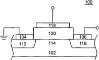
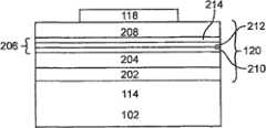
图1展示根据一示范性实施例的存储器装置100的详细横截面图。如图1中所示,存储器装置100形成于衬底102上。存储器装置100包括源极区112、沟道区114、漏极区116、控制栅极或栅极触点118、栅极堆叠120、源极触点104、漏极触点106。一般类似于晶体管配置而配置源极区112、沟道区114和漏极区116。栅极堆叠120形成于沟道区114上。或者可被称为控制栅极或栅极电极的栅极触点118形成于栅极堆叠120上。Figure 1 shows a detailed cross-sectional view of a
存储器装置100一般如上文针对具有电荷存储层的常规存储器所描述而操作。然而,电荷存储层存储器装置100包括栅极堆叠120。栅极堆叠120用于为存储器装置100提供电荷存储层和如下文进一步描述的其它特征。当存储器装置100经编程时,电子被转移到栅极堆叠120的电荷存储层且由其存储。栅极堆叠120可包括任何类型的电荷存储层或电荷存储媒介。下文描述示范性电荷存储层。
在当前实施例中,衬底102为半导体型衬底,且经形成以至少在沟道区114中具有P型或N型导电性。栅极触点118、源极触点104和漏极触点106提供到存储器装置100的电连接性。源极触点104形成为与源极区112接触。漏极触点106形成为与漏极区116接触。源极区112和漏极区116通常为衬底102的掺杂区,所述掺杂区具有不同于沟道区114的导电性的导电性。In the current embodiment, the
如图1所示,源极触点104耦合到一电位,例如接地电位。漏极触点106耦合到另一信号。注意,源极区112和漏极区116是可互换的,且其互连可颠倒。As shown in FIG. 1 ,
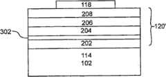
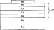
图2展示根据一个示范性实施例的栅极堆叠120的横截面图。在图2中,栅极堆叠120包括隧穿介电层202、电荷存储层204、电荷阻断层206和控制介电层208。在图2的实例中,隧穿介电层202形成于存储器装置100的衬底102的沟道区114上。电荷存储层204形成于隧穿介电层202上。电荷阻断层206形成于电荷存储层204上。控制介电层208形成于电荷阻断层206上。如图2所示,栅极触点118形成于控制介电层208上。或者,电荷阻断层206可形成于控制介电层208上,且栅极触点118可形成于电荷阻断层206上,如图11所示。注意,在示范性实施例中,一个或一个以上其它材料层可分离栅极堆叠120的层和/或可将栅极堆叠120与衬底102和/或栅极触点118分离。FIG. 2 shows a cross-sectional view of a
电荷存储层204存储正电荷或负电荷以指示存储器装置100的编程状态,如上文所描述。电荷存储层204可包括上文所描述或另外已知的材料。在编程期间,施加到栅极触点118的电压产生电场,所述电场使电子从沟道区114穿过隧穿介电层202而隧穿进入(例如,或经由热电子注射)电荷存储层204中。存储于电荷存储层204中的所得负电荷使存储器装置100的阈值电压偏移。甚至在从栅极触点118移除电压后电荷仍保留于电荷存储层204中。在擦除过程期间,可将反向充电的电压施加到栅极触点118以使电子从电荷存储层204穿过隧穿介电层202而排放到衬底102,或将空穴从沟道114隧穿(或经由沟道热空穴)隧道介电层202而汲取到电荷存储层204。控制介电层208使栅极触点118与电荷阻断层206隔离。The
栅极触点118优选由导电材料形成。举例来说,栅极触点118可由多晶硅(polycrystalline silicon/polysilicon)形成。在另一实例中,栅极触点118可由金属或包括一种或一种以上金属(例如,一种或一种以上过渡金属)的材料形成。可适合于栅极触点118的示范性过渡金属包括(但不限于):Ti、V、Cr、Mn、Fe、Co、Ni、Cu、Zn、Zr、Nb、Mo、Ru、Rh、Pd、Ag、Cd、Hf、Ta、W、Re、Os、Ir、Pt、Au和Hg。根据一个示范性实施例,栅极触点118可由TaN形成。
一般来说,栅极触点118的厚度在约5nm到约5,000nm的范围内。优选地,栅极触点118的厚度在约10nm到约500nm的范围内。根据一个示范性实施例,栅极触点118可包括多个子层。每一子层可由不同导电材料形成。Generally, the
可通过此项技术中已知的气相沉积技术而形成栅极触点118。物理气相沉积(PVD)技术(例如,溅镀或热蒸镀)、化学气相沉积(CVD)或原子层沉积(ALD)可适于栅极触点118的沉积。
电荷存储层204可包括任何类型的电荷存储媒介。优选地,电荷存储层204为包括多个离散电荷存储元件的局部化(localized)电荷存储层。离散电荷存储元件可为一个或一个以上局部化电荷陷阱(例如在氮化物层中发现的那些电荷陷阱)或半导体纳米粒子、金属纳米粒子或介电纳米粒子(量子点)。举例来说,电荷存储层204可包括由例如钌(Ru)等高功函数(例如,大于4.5eV)金属形成的且优选具有小于约5nm的大小的纳米晶体。如此项技术中已知,这些纳米晶体可通过多种工艺(例如,化学气相沉积(CVD)、原子层沉积(ALD)或物理气相沉积(PVD))而沉积于隧穿介电层202上。电荷存储层204也可包括沉积于隧穿介电层202上的预先形成的胶状金属或半导体或介电量子点(纳米晶体)。举例来说,例如在每一者以全文引用的方式并入本文中的第6,586,785号美国专利、第11/147,670号美国申请案和第11/495,188号美国申请案中所描述的,可通过例如旋涂、喷涂、印刷、化学组装、使用聚合物自组装的纳米压印等方法来沉积此些材料。电荷存储层204也可包括连续金属或半导体导电层、不连续金属或半导体导电层、基于不导电氮化物的或其它类型的绝缘电荷捕集层、具有安置于其中的导电元件(例如,硅岛)的不导电氧化物层(例如,SiO2)、经掺杂氧化物层等。为进一步描述包括氮化物的电荷存储层,参考以全文引用的方式并入本文中的第5,768,192号美国专利。根据一个示范性实施例,当沿存储器单元的字线方向以横截面观看时,电荷存储层可具有U形。
当例如钌(或其它金属或合金)等金属量子点用于电荷存储材料时,隧穿介电层202(也称为“隧道介电层”)的表面可变更,以提供对金属迁移的改进的障壁。举例来说,如图3所示,栅极堆叠120′可包括形成于隧穿介电层202上的在隧穿介电层202与电荷存储层204之间的障壁层302。障壁层302可包括(例如)例如氮化物(Si3N4)或氮氧化硅(SiOxNy,其中x和y为正数,0.8、1.5等)等含氮化合物或例如氧化铝(Al2O3)等其它合适障壁层。障壁层302改变隧穿介电层202的表面结构,使得可使金属迁移效应最小化。在障壁层302由氮化合物制成的情况下,可通过添加氮或“含氮”化合物(例如,“氮化”)到隧穿介电层202(例如,其可为SiO2)而形成含氮层。在一示范性实施例中,可使用例如低压CVD(LPCVD)或超高真空CVD(UHVCVD)的化学气相沉积(CVD)工艺而将氮或含氮化合物沉积于隧穿介电层202上。含氮层可与隧穿介电层202直接接触。When metal quantum dots such as ruthenium (or other metals or alloys) are used in the charge storage material, the surface of the tunneling dielectric layer 202 (also referred to as "tunneling dielectric") can be altered to provide improved metal transport barrier. For example, as shown in FIG. 3 , the
障壁层302的UHVCVD可比LPCVD更可控制,因为UHVCVD一般更缓慢地发生,且因此生长率可受到更精密地调节。可由于从例如硅烷(或例如二氯硅烷或二硅烷等其它硅源前驱体)与氨(或例如经等离子体离子化的氮等其它氮物质,N2O或NO)的气体的反应,或例如氨(或例如经等离子体离子化的氮的其它氮物质,N2O或NO)等反应气体的表面反应的沉积而形成含氮层。二氯硅烷和氨气与某惰性气体与含氧气体的同向流动可用于含氮层的生长。障壁层302阻止电荷存储层204的金属纳米粒子/量子点穿入隧穿介电层202中,使得避免可导致泄漏的隧道介电层202的污染。UHVCVD of the
障壁层302的厚度优选经配置以确保包括于氮化物结构中的载流子陷阱不支配所形成的半导体装置的电荷存储方面。在一示范性实施例中,障壁层302的所要厚度小于约10埃。在其它实施例中,所要厚度可为约5埃或更小。隧穿介电层202与障壁层302的相对厚度可经裁剪以优化电性能和金属迁移障壁功能。障壁层302的厚度应为至少确保隧穿介电层202被障壁层302大体均匀覆盖所需的厚度。优选地,障壁层302的厚度为至少约1埃。在将氮氧化硅用作障壁层302的示范性实施例中,氮氧化硅内的氮的浓度可(例如)大于约5%。可控制包括于氮氧化硅中的氮的百分比浓度,使得可调节氮化物层抵制来自金属量子点(当在电荷存储层204中时)的金属迁移的障壁功能与由于氮化物浓度而包括陷阱之间的折衷。The thickness of
在一示范性实施例中,隧穿介电层202为SiO2且衬底102为硅。控制介电层208可由单一成分氧化物(例如,Al2O3或SiO2)形成。据信SiO2作为控制介电层208可能是有利的,因为其形成对电子隧穿的高能量障壁(例如,见图4B)。而且,SiO2含有很少的电荷陷阱(charge trap),且据信存在于层中的那些电荷陷阱充分深,使得其不会妨碍装置的电荷保留。根据一替代实施例,控制介电层208可由例如多成分氧化物的多成分材料形成。In an exemplary embodiment, the
控制介电层208优选具有不大于约20nm的厚度。据信控制介电层的厚度由于新一代存储器装置缩放到较小横向尺寸而较重要。因为存储器单元的沟道长度和装置宽度减小到约30nm以下,所以需要将介电层的厚度减少到小于沟道长度,使得控制栅极可维持耦合到电荷存储层。根据一示范性实施例,控制介电层208的厚度为约15nm或更小。控制介电层208的厚度也可为约10nm或更小。根据一优选实施例,控制介电层208具有约5nm或更小的厚度。举例来说,控制介电层208的厚度可为约4nm或更小、约3nm或更小、约2nm或更小或者约1nm或更小。控制介电层208的厚度也优选至少为确保大体均匀覆盖下伏层所需的厚度。因此,控制介电层208的厚度优选为至少约0.1nm。
优选地,控制介电层208的厚度不大于电荷阻断层206的厚度的约200%。更优选地,控制介电层208的厚度不大于电荷阻断层206的厚度的约150%。举例来说,根据一个示范性实施例,电荷阻断层206的厚度为约4nm,且控制介电层208的厚度为约5nm或为电荷阻断层206的厚度的约125%。在其它示范性实施例中,控制介电层208的厚度不大于电荷阻断层206的厚度的约125%,或不大于电荷阻断层206的厚度的约100%。还预期控制介电层208的厚度小于电荷阻断层206的厚度的情况。Preferably, the thickness of the
在一示范性实施例中,电荷阻断层206由高k介电材料形成。出于本发明的目的,高k介电材料具有高于SiO2的介电常数的介电常数(例如,3.9)。电荷阻断层206的高k介电材料可为(例如)Al2O3、HfO2、HfSiO2、ZrO2、Hf1-xAlxOy(其中x为在0与1之间的正数,且y为正数,例如HfAlO3等),优选为HfO2或Hf1-xAlxOy(其中x为在0与1之间的正数,且y为正数,例如HfAlO3)。在其它实施例中,例如,电荷阻断层206可由其它高k介电材料形成,其它高k介电材料例如为Gd2O3、Yb2O3、Dy2O3、Nb2O5、Y2O3、La2O3、ZrO2、TiO2、Ta2O5、SrTiO3、BaxSr1-xTiO3、ZrxSi1-xOy、HfxSi1-xOy、AlxZr1-xO2或Pr2O。In an exemplary embodiment, the
在示范性实施例中,电荷阻断层206具有高于控制介电层208的介电常数。举例来说,在一个实施例中,当沉积时,控制介电层208为Al2O3,其具有约为9的介电常数,且电荷阻断层206为HfO2,其具有小于约为25的介电常数(例如,22左右)。在另一实施例中,控制介电层208为SiO2,其具有约为4的介电常数,而电荷阻断层为HfO2。In an exemplary embodiment, the
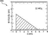
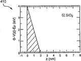
图4A-4C包括曲线图400、410、420,其示意性地展示包括邻近于较低介电常数的介电层的较高介电常数的介电层(例如,电荷阻断层206)可如何改进隧穿电阻。图4A的曲线图400展示仅具有较高介电常数的介电层(例如,HfO2)的能量障壁(eV),且图4B的曲线图410展示仅具有较低介电常数的介电层(例如,SiO2)的能量障壁。较低k介电层(SiO2)提供比较高k介电层(HfO2)提供的隧穿能量障壁高的隧穿能量障壁,但较高k介电层(HfO2)提供较宽的障壁。图4C的曲线图420展示在较高k介电层(例如,HfO2)邻近于较低k介电层(例如,SiO2)而安置时隧穿障壁的量值的改进。因此,可减小隧穿电流。较高k电介质与较低k电介质的任意组合可适于电荷阻断层206和控制介电层208。优选地,如上文所述,电荷阻断层206具有较高介电常数(例如,较低障壁高度),且控制介电层208具有较低介电常数(例如,较高障壁高度)。4A-4C include
在示范性实施例中,电荷阻断层206在层206的整个厚度中可包括组成、带隙值和/或介电常数的梯度。梯度可从电荷阻断层206的第一表面(例如,电荷阻断层206的邻近于电荷存储层204的表面)到电荷阻断层206的第二表面(例如,电荷阻断层206的邻近于控制介电层208的表面)增大或减小。In an exemplary embodiment,
举例来说,具有组成梯度的电荷阻断层206可包含介电材料,且介电材料的至少一个成分的量可在电荷阻断层206的厚度上变化。优选地,介电材料为高k介电材料。成分的量可在电荷阻断层206的厚度上线性地、非线性地或步进地变化。优选地,成分的量在控制介电层208附近处为最小且在电荷阻断层206的厚度上增加。所述成分可为元素或化合物。举例来说,所述成分可为铪或氧化铪。根据一示范性实施例,具有组成梯度的电荷阻断层206由多成分介电材料形成。举例来说,电荷阻断层206可由例如HfxAl1-xOy、HfxSi1-xOy、ZrxSi1-xOy、BaxSr1-xTiOy或AlxZr1-xOy等多成分氧化物形成。根据一示范性实施例,多成分介电材料可包括所述成分(例如,铪)和第二成分,且所述成分与第二成分的比率可在电荷阻断层206的厚度上变化。多成分介电材料可包括氮。举例来说,根据一示范性实施例,多成分介电材料可为HfxSi1-xO2-yNy。具有组成梯度的电荷阻断层206可安置于电荷存储层204与控制介电层208之间,或安置于控制介电层208与存储器装置100的栅极触点118之间。For example, the
在另一示范性实施例中,电荷阻断层206包含多个材料层。图5展示(例如)包括三个层的电荷阻断层206。根据此示范性实施例,电荷阻断层206包括最接近电荷存储层204的第一层210、第二(中间)层212和第三层214(距电荷存储层204最远)。根据一个实施例,最接近电荷存储层204的层由相对高带隙材料形成,而距电荷存储层204较远的一个或一个以上层由具有逐渐降低的带隙的一种或一种以上材料形成。当电荷存储层204包含隔离粒子(例如,纳米粒子、量子点)时此可为需要的,因为相对较高带隙材料与较低带隙材料相比允许粒子之间的较少隧穿。SiO2、Al2O3、HfAlO3为具有相对高带隙的示范性材料。如所属领域的技术人员将认识到,替代实施例将包括最接近电荷存储层204的由相对低带隙材料形成的层,和距电荷存储层204较远的由具有逐渐变高的带隙的一种或一种以上材料形成的一个或一个以上层。In another exemplary embodiment, the
根据电荷阻断层206的一示范性三层实施例,第一层210可为Al2O3,第二(中间)层212可为HfAlO3,且第三层214可为HfO2(其具有相对低的带隙)。在电荷阻断层206的一示范性二层实施例中,第一层(最接近电荷存储层204)可为SiO2,且第二层可为HfO2,其具有相对高的介电常数(用于有效的电荷阻断)和低带隙。如上文所描述,控制介电层208可为例如Al2O3或SiO2等材料。According to an exemplary three-layer embodiment of the
在一示范性实施例中,电荷阻断层206可经掺杂。举例来说,电荷阻断层206可掺杂有例如稀土金属、过渡金属、硅、氧或氮等掺杂剂材料。根据一个示范性实施例,电荷阻断层206可为Hf1-xSixO2-yNy。可通过后沉积氮化处理而引入氮。举例来说,Hf1-xSixO2层可在含有NH3、N2O或NO的环境中退火以形成Hf1-xSixO2-yNy层。In an exemplary embodiment, the
在一示范性实施例中,电荷阻断层206经形成为相对较薄(例如小于约10nm,例如小于约5nm,例如小于约2nm),以减少电子被电荷阻断层206的高介电材料捕集。优选地,电荷阻断层206具有足以确保大体均匀覆盖下伏层的厚度。举例来说,电荷阻断层206可为至少0.1nm厚。优选地,电荷阻断层206为至少0.5nm厚。In an exemplary embodiment, the
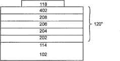
图6展示根据一示范性实施例的栅极堆叠120″的另一横截面图。除在图6中栅极堆叠120″进一步包括形成于控制介电层208上的第二电荷阻断层402外,图6中的栅极堆叠120″的配置大体类似于图2。在图6中,栅极触点118形成于第二电荷阻断层402上。在一示范性实施例中,第二电荷阻断层402由例如Al2O3、HfO2、ZrO2、Hf1-xAlxOy(其中x为在0与1之间的正数,且y为正数,例如HfAlO3、Hf1-xSixO2、Hf1-xSixO2-yNy等)等高k介电材料形成。第二电荷阻断层402可由上文针对第一电荷阻断层206所述的材料中的任一者形成,且可以类似方式(例如以单层配置(均匀材料或材料梯度)或多层配置)配置。FIG. 6 shows another cross-sectional view of the
根据第二电荷阻断层402包括组成梯度的一示范性实施例,第二电荷阻断层402可包含介电材料,且介电材料的至少一个成分的量可在电荷阻断层402的厚度上变化。优选地,介电材料为高k介电材料。成分的量可在第二电荷阻断层402的厚度上线性地、非线性地或步进地变化。优选地,所述成分的量在控制介电层208附近处为最小且在第二电荷阻断层402的厚度上增加。所述成分可为元素或化合物。举例来说,所述成分可为铪或氧化铪。According to an exemplary embodiment in which the second
根据一示范性实施例,具有组成梯度的第二电荷阻断层402由多成分介电材料形成。举例来说,第二电荷阻断层402可由例如HfxAl1-xOy、HfxSi1-xOy、ZrxSi1-xOy、BaxSr1-xTiOy或AlxZr1-xOy等多成分氧化物形成。根据一示范性实施例,多成分介电材料可包括所述成分(例如,Hf)和第二成分,且所述成分与所述第二成分的比率可在第二电荷阻断层402的厚度上变化。多成分介电材料可包括氮。举例来说,根据一示范性实施例,多成分介电材料可为HfxSi1-xO2-yNy。具有组成梯度的第二电荷阻断层402可安置于控制介电层208与存储器装置100的栅极触点118之间,或安置于电荷存储层204与控制介电层208之间。According to an exemplary embodiment, the second
电荷阻断层206与402(其夹住控制介电层208)可有效地阻断电荷输送穿过控制介电层208。举例来说,第一电荷阻断层206(例如,HfO2)可在编程操作期间阻断从电荷存储层204到栅极触点118的电子流。第二电荷阻断层402(例如,HfO2)可在擦除操作期间阻断从栅极触点118到电荷存储层204的电子流。另外,第一电荷阻断层206和/或第二电荷阻断层402可具有其它功能。在一示范性实施例中,第一电荷阻断层206和第二电荷阻断层402的厚度较薄,例如小于10nm,例如小于5nm。The charge blocking layers 206 and 402 (which sandwich the control dielectric layer 208 ) effectively block charge transport through the
第一电荷阻断层206和第二电荷阻断层402的另一优点在于:尽管高k介电层自身可具有陷阱,但是第一电荷阻断层206和第二电荷阻断层402可被制得非常薄(例如小于约4nm,例如小于2nm)以减少电荷陷阱的总量,同时有效地阻断电流流动。此外,第二电荷阻断层402邻近于栅极触点118而定位。因此,即使在第二电荷阻断层402中捕集相较大量的电荷,对平带电压的影响仍与第二电荷阻断层402到栅极触点118的距离成比例,所述距离为最小(因为其可彼此直接邻近(接触))。Another advantage of the first
图6的实施例(其中第一电荷阻断层206和第二电荷阻断层402为HfO2,且控制介电层208为Al2O3)的一些其它示范性优点包括:Some other exemplary advantages of the embodiment of FIG. 6 in which the first
(1)可实现存储器编程/擦除窗的增强。如本文所使用,编程/擦除(P/E)窗为编程状态的阈值状态与擦除状态的阈值状态之间的电压差。通过栅极堆叠120″,可使用12.8V或更大的P/E窗口来擦除(例如,直到-6V)存储器装置100。在示范性实施例中,P/E窗口可在从约8V到约16V的范围中(例如,在约9V到约14V、约10V到约13V的范围中或具有约9V、约10V、约11V、约12V或约13V的值)。在+/-20V的P/E界限内将隧穿介电层202缩放到6nm的情况下,P/E窗口可大达14.2V,接近例如3位或甚至4位存储器单元的多态存储器电压要求;(1) Enhancement of the memory programming/erasing window can be realized. As used herein, the program/erase (P/E) window is the voltage difference between the threshold state of the programmed state and the threshold state of the erased state. With the
(2)在100,000次P/E循环后P/E窗口可不展示显著漂移;以及(2) the P/E window may not exhibit significant drift after 100,000 P/E cycles; and
(3)电荷可在12V的P/E窗口下保留于电荷存储层204中,且更重要地,100,000次P/E循环可能不会降低电荷保留特性。(3) Charges can be retained in the
在存储器装置100的一些示范性实施例中,电荷存储层204为单一连续区。举例来说,图7展示具有平坦、连续配置的电荷存储层204的平面图。举例来说,电荷存储层204可由硅(或多晶硅)、金属等的连续膜形成。在此配置中,如果连续区的单点击穿且开始失去电荷,则整个区可失去其电荷,从而使存储器装置100失去其编程状态。然而,一些实施例可提供对此问题的某种防护。举例来说,图8展示根据一示范性实施例的具有非连续配置的电荷存储层204的平面图。在图8的实例中,电荷存储层204包含多个纳米粒子802。因为电荷存储层204的纳米粒子802各自单独地存储电荷且彼此绝缘,所以即使单一纳米粒子失去电荷,此也将不大可能影响电荷存储层204的剩余纳米粒子。使用将电荷存储于局部化电荷陷阱区中的基于不导电氮化物的电荷存储层可获得相同的优点。因此,根据本发明的并入有电荷存储层204的存储器装置与常规存储器装置相比可在极长的时间内维持恒定的编程状态。In some exemplary embodiments of
在一示范性实施例中,纳米粒子802为电隔离纳米晶体。纳米晶体为彼此电隔离的导电材料的较小簇或晶体。一般来说,纳米晶体具有约100nm或更小的微晶大小。将纳米晶体用于电荷存储层204的一个优点在于其并不形成连续膜,且因此由纳米晶体形成的电荷存储层自隔离。因为纳米晶体形成非连续膜,所以电荷存储层可经形成而不必担心一个单元层级的电荷存储媒介与直接位于上方或下方的(即,垂直邻近)邻近单元的电荷存储媒介短路。将纳米晶体用于电荷存储层的又一优点在于其可经历比连续膜电荷存储层少的电荷泄漏。In an exemplary embodiment,
纳米晶体可由导电材料形成,导电材料例如为钯(Pd)、铱(Ir)、镍(Ni)、铂(Pt)、金(Au)、钌(Ru)、钴(Co)、钨(W)、碲(Te)、铼(Re)、钼(Mo)、铁铂合金(FePt)、钽(Ta)、氮化钽(TaN)等。此些材料一般具有比许多半导体(例如,硅)高的功函数(例如,约4.5eV或更高),这是多电子存储所需的。所述材料也可具有较高熔点(其允许较高的热预算),具有较长保留时间且具有高密度的正电荷存储状态与负电荷存储状态。Nanocrystals can be formed from conductive materials such as palladium (Pd), iridium (Ir), nickel (Ni), platinum (Pt), gold (Au), ruthenium (Ru), cobalt (Co), tungsten (W) , tellurium (Te), rhenium (Re), molybdenum (Mo), iron-platinum alloy (FePt), tantalum (Ta), tantalum nitride (TaN), etc. Such materials generally have a higher work function (eg, about 4.5 eV or higher) than many semiconductors (eg, silicon), which is required for multi-electron storage. The material may also have a higher melting point (which allows for a higher thermal budget), have a longer retention time, and have a high density of positive and negative charge storage states.
用于形成纳米晶体的方法为此项技术中众所周知的,例如,如2006年8月18日申请的第11/506,769号美国申请案中所揭示,其揭示内容以全文引用的方式并入本文中。可通过物理气相沉积(PVD)或原子层沉积(ALD)而形成金属纳米晶体电荷存储层,其中首先将薄膜沉积于衬底表面上(例如,通过使用PVD的溅镀)且接着在高温(例如,约摄氏900度或更高)下退火并持续较短时间(例如,约10秒)以聚结纳米级的金属粒子。可通过使经溅镀的金属层的厚度、退火温度和退火时间、压力和周围气体物质等变化来控制金属粒子的均匀性和大小。当硅纳米晶体用于电荷存储层204中时,可通过例如CVD(如(例如)第6,297,095号美国专利中所描述,所述专利以全文引用的方式并入本文中)等工艺而形成硅纳米晶体。电荷存储层204可包括通过例如旋涂、喷涂、印刷、化学自组装等方法而沉积于隧穿介电层202上的预先形成的胶状金属或半导体量子点。举例来说,在每一者以全文引用的方式并入本文中的第6,586,785号美国专利、第11/147,670号美国申请案和第11/495,188号美国申请案中描述了此些工艺。Methods for forming nanocrystals are well known in the art, for example, as disclosed in U.S. Application Serial No. 11/506,769, filed August 18, 2006, the disclosure of which is incorporated herein by reference in its entirety . Metal nanocrystal charge storage layers can be formed by physical vapor deposition (PVD) or atomic layer deposition (ALD), where a thin film is first deposited on a substrate surface (e.g., by sputtering using PVD) and then heated at a high temperature (e.g., , about 900 degrees Celsius or higher) for a short time (eg, about 10 seconds) to coalesce the nanoscale metal particles. The uniformity and size of the metal particles can be controlled by varying the thickness of the sputtered metal layer, annealing temperature and time, pressure, and surrounding gas species. When silicon nanocrystals are used in the
另外,替代在存储器装置100中包括用于电荷存储的电介质隔离的电荷存储层,可使用形成于栅极堆叠的介电堆叠中的不导电捕集层。举例来说,电荷存储媒介可为介电堆叠,其包含邻近于沟道区114的第一氧化物层(例如,隧穿介电层202)、邻近于第一氧化物层的不导电氮化物层和邻近于氮化物层且邻近于栅极触点118的第二氧化物层。此介电堆叠有时被称为ONO堆叠(即,氧化物-氮化物-氧化物)堆叠。第二氧化物层可被栅极堆叠120、120′或120″中的一者取代以改进传统ONO堆叠的性能。如果需要,则可使用例如含H+氧化膜的其它合适的电荷捕集介电膜。Additionally, instead of including a dielectrically isolated charge storage layer for charge storage in the
示范性实施例exemplary embodiment
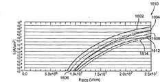
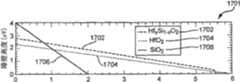
在一示范性实施例中,电荷存储层204包括金属点,电荷阻断层206为HfO2,且控制介电层208为Al2O3。图9A展示电荷阻断层206(HfO2)与控制介电层208(Al2O3)的组合控制电介质的能量(eV)对厚度(nm)的仿真曲线图900。图9B展示电流(A/cm2)对电场(V/cm)的仿真曲线图920。所述曲线图包括仅包括HfO2的组合控制电介质的曲线902,和仅包括Al2O3的组合控制电介质的曲线904。对于曲线902与曲线904两者,未指示障壁降低。图9A和图9B中的数据展示在金属与Al2O3的界面处包括HfO2的薄层可使电子隧穿电流减少许多数量级。即使HfO2层为小于1nm厚也是如此。In an exemplary embodiment, the
图10A-10C展示关于类似于图2所示的栅极堆叠120的示范性栅极堆叠的曲线图1000、1010和1020。如图10B所示,对于总共13V的P/E窗口,擦除电压为约-3.7V且编程电压为约9.3V。10A-
图11A和图11B展示类似于图6所示的栅极堆叠120″的示范性栅极堆叠的编程电压和擦除电压的曲线图1100、1120。在此实例中,电荷存储层204由量子点形成,第一电荷阻断层206由具有4nm厚度的HfO2形成,控制介电层208由12nm厚的Al2O3形成,且第二电荷阻断层402由4nm厚的HfO2形成。如由图11A和图11B中的数据所指示,P/E线性窗口为约11.39V。11A and
图11C和图11D分别展示类似于图6所示的栅极堆叠120″的示范性栅极堆叠的编程电压和擦除电压的曲线图1130和1140。在此实例中,电荷存储层204由量子点形成,第一电荷阻断层206由具有4nm厚度的HfO2形成,控制介电层208由12nm厚的Al2O3形成,且第二电荷阻断层402由8nm厚的HfO2形成。如由图11C和图11D中的数据所指示,P/E线性窗口为约12.76V。FIGS. 11C and 11D show
在另一示范性实施例中,存储器装置的栅极堆叠可包括作为电荷存储层的氮化物层、作为控制介电层的Al2O3层和作为电荷阻断层的例如HfO2等含铪化合物。如图12所示,根据此实施例,电荷阻断层206可形成于控制介电层208上方且邻近于控制栅极118。如上文所述,栅极堆叠可包括一个(或一个以上)其它电荷阻断层,例如在控制介电层下方且邻近于氮化物层的电荷阻断层。图13展示擦除时间(x轴)对平带电压(y轴)的图表1300,其中将不具有一个(或一个以上)电荷阻断层的常规栅极堆叠(参考数字1304)与上文所描述的将氮化物层用作电荷捕集层并使用邻近于控制介电层(例如,Al2O3)而形成的电荷阻断层(例如,HfO2)的改进的栅极堆叠(参考数字1302)进行比较。图14展示使用由图13中参考数字1302表示的改进的栅极堆叠的情况下将编程和擦除循环的数目(x轴)与平带电压(y轴)进行比较的图表1400。图14展示使用改进的栅极堆叠的情况下室温电荷保留映射时间(x轴)对平带电压(y轴)的图表。In another exemplary embodiment, a gate stack of a memory device may include a nitride layer as a charge storage layer, anAl2O3 layer as a control dielectric layer, and a hafnium-containing compound such asHfO2 as a charge blocking layer. compound. As shown in FIG. 12 , according to this embodiment, a
如图13中首先展示,与仅包括Al2O3控制介电层而不具有电荷阻断层的常规栅极堆叠1304相比,使用包含形成于控制介电层(例如,Al2O3)上的电荷阻断层(例如,HfO2)与氮化物电荷捕集层的改进的栅极堆叠1302展示存储器P/E窗口(例如,约2伏或更大)的增强。具有改进的栅极堆叠的此存储器装置具有总共大于约8伏的P/E窗口,据信所述P/E窗口为在将氮化物层用作电荷捕集层的情况下迄今为止在文献中报告的最高P/E窗口。另外,如图14的曲线图1400中所示,在使用改进的栅极堆叠实施例情况下,在100,000次P/E循环后,P/E窗口并未展示显著漂移。而且,如图15的曲线图1500中所示,在使用改进的栅极堆叠情况下,在大于8V的P/E窗口下电荷被保留,且100,000次P/E循环并未降低存储器装置的电荷保留特性。As first shown in FIG. 13 , compared to aconventional gate stack1304 comprising only an Al2 O3 control dielectric layer without a charge blocking layer, using The improved
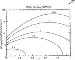
在另一示范性实施例中,电荷阻断层206为HfO2且控制介电层208为SiO2。图16A展示各种介电层的能量(eV)对厚度(nm)的仿真曲线图1600,包括单独SiO2(数据线1602)、单独HfO2(数据线1604)和HfO2与SiO2的组合(数据线1606、1608、1612、1614)。图16B展示相同介电层的福勒-诺德汉姆(Fowler-Nordheim)隧穿电流密度(A/cm2)对电场(V/cm)的仿真曲线图1610。计算出的数据展示在导体(例如,具有功函数4.8eV的金属)与SiO2之间的界面处包括HfO2的薄层可将电子隧穿减少若干数量级。In another exemplary embodiment, the
在另一示范性实施例中,电荷阻断层206为HfxSi1-xO2且Hf的量(x)在电荷阻断层的厚度(z)上变化,如图17A的曲线图1700中所示。在此图中,Hf的量以非线性方式远离界面(z=0)而减少。用以抑制电子隧穿的电荷阻断层的最佳组成和厚度取决于电场强度。对于20MV/cm的电场强度(Esio2)而言,数据是最佳的。图17B展示与HfO2层和SiO2层的障壁高度相比,变化的Hf含量的HfxSi1-xO2层的障壁高度(eV)对距界面的距离(z)的仿真曲线图1710。类似地,图17C展示对于变化的Hf含量的HfxSi1-xO2层,介电常数(ε)在层(z)上的变化的仿真曲线图1720。还展示HfO2层和SiO2层的介电常数。通过参考数字1702、1704和1706来分别表示HfxSi1-xO2、HfO2和SiO2的数据线。In another exemplary embodiment, the
图18中的曲线图1800展示对于给定电场强度,HfxSi1-xO2层的最佳Hf含量(x)如何根据电压而变化。
图19A的曲线图1900展示在以下组成:HfxSi1-xO2/SiO2/HfxSi1-xO2的电荷阻断层/控制介电层/电荷阻断层结构上对于各种电场强度的最佳Hf含量(x)。数据线1902、1904、1906和1908分别对应于15MV/cm、20MV/cm、25MV/cm和30MV/cm的电场强度。对于7nm的等效氧化物厚度(EOT),在20MV/cm的电场强度下,最佳薄膜组成大致为Hf2/3Si1/3O2(4.5nm)/SiO2(5nm)/Hf2/3Si1/3O2(4.5nm)。The graph1900ofFIG .19Aisshown for each The optimal Hf content (x) for each electric field strength.
图19B的曲线图1910展示对于与图19A中相同的层结构和组成且还对于SiO2、HfO2和对于HfO2(4nm)/SiO2(5.4nm)/HfO2(4nm)(分别为数据线1912、1914和1916),福勒-诺德汉姆(Fowler-Nordheim)隧穿电流密度根据电场强度而变化。可通过使用组成上分级的电介质作为电荷阻断层而将隧穿电流减少超过两个数量级。数据展示可在等于SiO2中的2.5×107V/cm的电场强度的电场强度下将隧穿电流维持在小于约10-4A/cm2。因此,通过使用经优化的电荷阻断层,存储器装置的总的动态线性范围可扩展到±10V与Vg~±25V。
图19C和19D的曲线图1920和1930分别展示对于上文提及的层结构和组成,针对各种电场强度所计算的能带图。
先前的图中呈现的各种数据是使用文泽尔-克莱姆斯-布里娄因(Wentzel-Kramers-Brillouin(WKB))近似而计算的,其中ψ(x)表示隧道障壁中的波函数且k(z)表示波向量的虚部:The various data presented in the previous figures were calculated using the Wentzel-Kramers-Brillouin (WKB) approximation, where ψ(x) represents the wave in the tunnel barrier function and k(z) represents the imaginary part of the wave vector:

为使隧穿电流ψ(x)最小化,使


因此,对于每一V(z),使


据信上述计算程序对于预测本文所描述的介电层、栅极堆叠和/或存储器装置的特性(behavior)是有用的;然而,此计算程序不应用于限制本发明的范围。The calculation procedures described above are believed to be useful for predicting the behavior of the dielectric layers, gate stacks, and/or memory devices described herein; however, such calculation procedures should not be used to limit the scope of the invention.
多态存储器实施例Multi-state memory embodiment
存储器装置可具有任何数目的存储器单元。在常规单位存储器单元中,存储器单元假定两个信息存储状态中的一者,“导通”状态或“断开”状态。“导通”或“断开”的双值条件(binary condition)界定信息的一个位。结果,能够存储数据的n个位的常规存储器装置要求(n)个单独的存储器单元。A memory device may have any number of memory cells. In a conventional unitary memory cell, the memory cell assumes one of two information storage states, an "on" state or an "off" state. A binary condition that is "on" or "off" defines a bit of information. As a result, a conventional memory device capable of storing n bits of data requires (n) individual memory cells.
可使用每单元存储器装置单一位的方式存储的位的数目取决于存储器单元的数目。因此,增加存储器容量要求含有更多存储器单元的较大裸片大小,或使用改进的光刻技术来产生较小的存储器单元。较小的存储器单元允许在单一裸片的给定区域内放置更多存储器单元。The number of bits that can be stored using a single bit per cell memory device depends on the number of memory cells. Therefore, increasing memory capacity requires larger die sizes containing more memory cells, or the use of improved lithographic techniques to produce smaller memory cells. Smaller memory cells allow more memory cells to be placed within a given area of a single die.
单位存储器单元的替代方案为多位或多态存储器单元,其可存储数据的一个以上位。可通过产生具有多个不同阈值电压电平(Vt1-n)的存储器单元来生产多位或多态快闪存储器单元,如(例如)以全文引用的方式并入本文中的第5,583,812号美国专利中所描述。每一不同阈值电压电平(Vt1-n)对应于一组数据位的一值,其中位的数目表示可存储于多态存储器单元中的数据量。因此,多个二进制数据位可存储于同一存储器单元中。An alternative to single-bit memory cells is a multi-bit or multi-state memory cell, which can store more than one bit of data. Multi-bit or multi-state flash memory cells can be produced by creating memory cells with multiple different threshold voltage levels (Vt1-n ), such as, for example, U.S. No. 5,583,812, which is incorporated herein by reference in its entirety. described in the patent. Each distinct threshold voltage level (Vt1-n ) corresponds to a value for a set of data bits, where the number of bits represents the amount of data that can be stored in the multi-state memory cell. Thus, multiple bits of binary data can be stored in the same memory cell.
可存储于多态存储器单元中的每一二进制数据值对应于一阈值电压值或值的范围,多态存储器单元在所述范围内传导电流。多态存储器单元的多个阈值电压电平彼此分离足够的量,使得可以明确的方式编程或擦除多态存储器单元的电平。被编程到存储器单元中的数据与单元的阈值电压电平之间的特定关系取决于多态存储器单元所采用的数据译码方案。Each binary data value storable in a multi-state memory cell corresponds to a threshold voltage value or range of values over which the multi-state memory cell conducts current. The multiple threshold voltage levels of a multi-state memory cell are separated from each other by a sufficient amount such that the levels of the multi-state memory cell can be programmed or erased in a definite manner. The particular relationship between the data programmed into a memory cell and the cell's threshold voltage level depends on the data coding scheme employed by the multi-state memory cell.
在编程多态存储器单元中,在足够的时间周期内施加编程电压以将足够电荷存储于电荷存储层中,从而将多态存储器单元的阈值电压移动到所要电平。此电平表示多态存储器单元的对应于被编程到多态存储器单元中的数据的编码的状态。In programming a multi-state memory cell, a programming voltage is applied for a sufficient period of time to store sufficient charge in the charge storage layer to move the threshold voltage of the multi-state memory cell to a desired level. This level represents the state of the multi-state memory cell corresponding to the encoding of the data programmed into the multi-state memory cell.
根据各种示范性实施例,可通过电隔离的纳米粒子(例如图8中所示)或例如图7中所示的连续或不连续金属(或硅)层而将多态存储器单元/装置的多个阈值电压电平提供于电荷存储层204中。According to various exemplary embodiments, multi-state memory cells/devices may be integrated by electrically isolated nanoparticles (such as shown in FIG. 8 ) or continuous or discontinuous metal (or silicon) layers, such as shown in FIG. 7 . Multiple threshold voltage levels are provided in the
在多位存储器单元的另一实施例中,如(例如)以全文引用的方式并入本文中的第5,768,192号美国专利中所描述,将电荷存储于存储器单元的靠近装置的源极区和漏极区的相对侧上的两个物理上不同的区域中的不导电电荷捕集层(例如,氮化物层)中。通过显影单元中的对称和可互换的源极区和漏极区,产生两个非相互作用的物理上不同的电荷存储区,其中每一区域物理上表示信息的直接映像到存储器阵列的一个位且每一单元借此含有信息的两个位。单元的编程是在正向方向上执行,编程包括利用热电子注射将电荷注射到栅极内的电荷捕集材料中并持续足够的持续时间,使得电荷变得被不对称地捕集于电荷捕集材料中,电荷经注射直到栅极的阈值电压达到预定电平为止。接着在相反方向上读取单元,从相反方向编程单元。如(例如)以全文引用的方式并入本文中的第2004/0130941号美国申请公开案中所描述,此类型的多位存储器单元也可扩展到将离散金属纳米晶体用作电荷存储媒介的电荷存储层存储器装置。In another embodiment of a multi-bit memory cell, charge is stored in the source region and drain of the memory cell near the device as described, for example, in U.S. Patent No. 5,768,192, which is incorporated herein by reference in its entirety. In the non-conductive charge-trapping layer (eg, a nitride layer) in two physically distinct regions on opposite sides of the pole region. By developing symmetrical and interchangeable source and drain regions in the development cell, two non-interacting physically distinct charge storage regions are created, where each region physically represents a direct image of the information to one of the memory arrays bits and each cell thereby contains two bits of information. The programming of the cell is performed in the forward direction, which involves injecting charge into the charge-trapping material within the gate using hot electron injection for a sufficient duration that the charge becomes asymmetrically trapped in the charge-trapping material. In the collector material, charges are injected until the threshold voltage of the gate reaches a predetermined level. The cell is then read in the opposite direction, and the cell is programmed from the opposite direction. This type of multi-bit memory cell can also be extended to charge using discrete metal nanocrystals as the charge storage medium, as described, for example, in U.S. Application Publication No. 2004/0130941, which is incorporated herein by reference in its entirety. Storage layer memory device.
本发明人还已发现,可使用胶状金属纳米晶体(例如,如第6,586,785号美国专利和第11/147,670号和第11/495,188号美国申请案中所描述)来实现使用如上文所描述的不对称电荷存储的多位存储。严格控制此些胶状金属点(例如,在使用PVD或CVD的其它经沉积纳米晶体上)的大小和均匀性具有以下优点:在选择性地对靠近装置的源极和/或漏极的纳米晶体的一小部分充电以产生充电不对称时,通过使邻近点之间的横向电荷传导最小化而放宽对阈值范围(threshold spread)的要求。The present inventors have also discovered that colloidal metal nanocrystals (eg, as described in U.S. Patent No. 6,586,785 and U.S. Application Nos. 11/147,670 and 11/495,188) can be used to achieve Multi-bit storage with asymmetric charge storage. Tight control of the size and uniformity of such colloidal metal dots (e.g., on other deposited nanocrystals using PVD or CVD) has the advantage of selectively targeting nanocrystals near the source and/or drain of the device. When a small portion of the crystal is charged to create charging asymmetry, the threshold spread requirement is relaxed by minimizing lateral charge conduction between adjacent points.
本文所描述的装置和方法的使用的显著特征在于:通过使用(例如)用于产生如本文所描述的多态存储器的常规技术中的任一者,其可实现多个位在单一装置中的可靠存储。使用经由例如多电平接近等上述方法而实现的多位存储的常规快闪存储器遭受对阈值范围的控制的严格要求。然而,本示范性实施例可通过提供较大的编程/擦除窗口(约(例如)8伏或更大,或12伏或更大)、增加的编程/擦除速度和良好的电荷保留而克服常规快闪存储器装置的许多限制。此可允许各种阈值电压状态彼此之间的较大分离,使得可以明确的方式编程或擦除多态存储器单元的电平。A salient feature of the use of the devices and methods described herein is that, by using, for example, any of the conventional techniques used to produce multi-state memories as described herein, it enables multiple bits in a single device Reliable storage. Conventional flash memory using multi-bit storage implemented via the above methods such as multi-level access suffers from stringent requirements on the control of the threshold range. However, the present exemplary embodiment can be improved by providing a larger program/erase window (about, for example, 8 volts or greater, or 12 volts or greater), increased program/erase speed, and good charge retention Overcome many of the limitations of conventional flash memory devices. This can allow for greater separation of the various threshold voltage states from one another so that the levels of a multi-state memory cell can be programmed or erased in a definite manner.
本实施例也可进一步通过(例如)将电荷存储于电荷存储层中的两个不同存储位置的每一者中并进一步添加使用(例如)如上文所描述的多电压阈值电平将不同量或电荷状态存储于两个位置的每一者中的能力而实现每单元多个位(例如,三个或三个以上(例如,四个)位)的存储。电荷存储层可为(例如)纳米晶体层或不导电氮化物层,如上文所描述。通过将四个不同量的电荷存储于每一位置,存储器装置可借此存储电荷的4×4=16个不同组合,从而等于每单元提供四个位。在不损害电荷保留的情况下由本文所描述的教示提供的编程/擦除窗口的增强可通过提供存储媒介中的电荷的注射和检测的较大灵活性和对阈值范围的放宽要求而进一步实现多位存储能力。This embodiment can also be further enhanced by, for example, storing charge in each of two different storage locations in the charge storage layer and further adding a different amount or The ability to store charge states in each of the two locations enables storage of multiple bits per cell (eg, three or more (eg, four) bits). The charge storage layer can be, for example, a nanocrystalline layer or a non-conductive nitride layer, as described above. By storing four different amounts of charge at each location, the memory device can thereby store 4 x 4 = 16 different combinations of charges, equating to four bits per cell. The enhancement of the program/erase window provided by the teachings described herein without compromising charge retention can be further achieved by providing greater flexibility in the injection and detection of charge in the storage medium and relaxed requirements on the threshold range Multi-bit storage capability.
可根据众所周知的半导体制造技术来组装本文所描述的示范性实施例。图20展示提供用于形成电子装置(例如,存储器装置)的示范性程序的流程图2000。流程图2000是出于说明的目的而提供,但不意欲为限制性的。所属领域的技术人员基于以下论述将了解其它结构和操作实施例。没有必要一定以所示的次序来遵循流程图2000的程序。The exemplary embodiments described herein can be assembled according to well-known semiconductor fabrication techniques. 20 shows a
流程图2000开始于在衬底中形成源极区(2002)。举例来说,如图1所示,源极区112可形成于衬底102中。可根据常规掺杂或其它技术而形成源极区112。此外,在一示范性实施例中,源极触点104可根据常规沉积或其它技术而形成于源极区112上。
接下来,漏极区可形成于衬底中(2004)。举例来说,如图1所示,漏极区116可形成于衬底102中。可根据常规掺杂或其它技术而形成漏极区116。此外,在一实施例中,漏极触点106可根据常规沉积或其它技术而形成于漏极区116上。Next, a drain region may be formed in the substrate (2004). For example, as shown in FIG. 1 , drain
隧穿介电层可形成于衬底上(2006)。举例来说,如图2和图6所示,隧穿介电层202可形成于衬底102的沟道区114上。可根据常规氧化物生长或其它技术而形成隧穿介电层202。A tunneling dielectric layer can be formed on the substrate (2006). For example, as shown in FIGS. 2 and 6 , the
电荷存储层可形成于隧穿介电层上(2008)。举例来说,如图2和图6所示,电荷存储层204可形成于隧穿介电层202上。在一示范性实施例中,电荷存储层204直接形成于隧穿介电层202上。在另一实施例中,电荷存储层204形成于隧穿介电层202上所形成的中间层(例如,图3所示的障壁层302)上。A charge storage layer may be formed on the tunneling dielectric layer (2008). For example, as shown in FIGS. 2 and 6 , the
电荷存储层204可为金属或半导体材料层(连续或不连续)或粒子层,例如上文进一步描述的。可通过沉积技术而形成电荷存储层204,所述沉积技术例如为物理气相沉积(PVD)、化学气相沉积(CVD)、电化学沉积(ECD)、分子束外延法(MBE)、原子层沉积(ALD)或本文在别处描述或另外已知的其它技术。
电荷阻断层可形成于电荷存储层上(2010)。举例来说,如图2和图6所示,电荷阻断层206形成于电荷存储层204上。可根据本文在别处描述或另外已知的任何沉积技术(例如通过原子层沉积)而形成电荷阻断层206。在一示范性实施例中,如上文所描述,电荷阻断层206可被掺杂。此外,在另一示范性实施例中,如上文所描述,电荷阻断层206可形成为梯度或形成为具有多层。A charge blocking layer can be formed on the charge storage layer (2010). For example, as shown in FIGS. 2 and 6 , the
原子层沉积可特别适于形成包括组成梯度或多层的电荷阻断层206。举例来说,为了形成包含具有浓度在电荷阻断层206的厚度上变化的成分的介电材料的电荷阻断层206,可使用第一化学物质的第一前驱体来沉积介电材料的一个或一个以上第一单层,且接着可使用第二化学物质的第二前驱体来沉积介电材料的一个或一个以上第二单层,且接着可使用第三化学物质的第三前驱体来沉积介电材料的一个或一个以上第三单层,等等。换句话说,可使用不同前驱体来实行一个或一个以上单层的连续沉积,以形成包括组成梯度或多层的电荷阻断层206。还构想起初可沉积均匀组成的电荷阻断层206且接着可采用快速热退火(RTA)来实现成分分级层的效果。Atomic layer deposition may be particularly suitable for forming
控制介电层可形成于电荷阻断层上(2012)。举例来说,如图2和图6所示,控制介电层208形成于电荷阻断层206上。可根据本文别处所描述或另外已知的任何沉积技术(例如通过原子层沉积)而形成控制介电层208。A control dielectric layer may be formed on the charge blocking layer (2012). For example, as shown in FIGS. 2 and 6 , the
第二电荷阻断层可形成于控制介电层上(2014)。如图6所示,第二电荷阻断层402形成于控制介电层208上。可根据本文别处所描述或另外已知的任何沉积技术(例如原子层沉积)而形成第二电荷阻断层402。在一实施例中,以类似于第一电荷阻断层206的方式,可掺杂第二电荷阻断层402。此外,在一实施例中,以类似于第一电荷阻断层206的方式,可将第二电荷阻断层402形成为梯度或形成为具有多层。A second charge blocking layer may be formed on the control dielectric layer (2014). As shown in FIG. 6 , the second
没有必要在所有实施例中均形成第二电荷阻断层402。举例来说,图2展示不包括第二电荷阻断层的栅极堆叠120。在另一实例中,如图11所示,栅极堆叠120可包括控制介电层208上的电荷阻断层206,且可不形成第二电荷阻断层。It is not necessary to form the second
控制栅极可形成于栅极堆叠上(2016)。举例来说,如图2所示,栅极触点118形成于栅极堆叠120的控制介电层208上。如图6所示,栅极触点118形成于栅极堆叠120″的第二电荷阻断层402上。可根据常规沉积技术或其它技术而将栅极触点118形成于栅极堆叠120和120″上。A control gate can be formed on the gate stack (2016). For example, as shown in FIG. 2 , the
本文已描述改进的电子装置(例如可具有增强特性的存储器装置)的方法、系统和设备,增强特性包括增加的电荷保留、增强的存储器编程/擦除窗口、改进的可靠性和稳定性与单一或多态(例如,两个、三个或四个位)操作的可行性。Methods, systems, and apparatus have been described herein for improved electronic devices such as memory devices that may have enhanced characteristics including increased charge retention, enhanced memory program/erase windows, improved reliability and stability, and single or polymorphic (eg, two, three, or four bit) operation possibilities.
已揭示非易失性存储器装置中的多层控制电介质(例如,双层或三层控制电介质)的使用。多层控制电介质可在其中包括高k介电材料(例如,氧化铝(Al2O3)、氧化铪(HfO2)和/或氧化铝铪(HfAlOx,其中x为正整数,例如,1、2、3、4等)的混合膜)的组合。The use of multiple layers of control dielectrics (eg, double or triple layer control dielectrics) in non-volatile memory devices has been disclosed. The multilayer control dielectric may include therein a high-k dielectric material such as aluminum oxide (Al2 O3 ), hafnium oxide (HfO2 ), and/or hafnium aluminum oxide (HfAlOx , where x is a positive integer, eg, 1 , 2, 3, 4, etc.) combination of mixed membranes).
已描述用于存储器装置的双层控制介电层,包括(例如)Al2O3的控制介电层和HfO2(或Hf1-xAlxOy,其中x为0与1之间的正数,且y为正数,例如,HfAlO3)的电荷阻断层。HfO2层可提供在存储器装置的编程操作期间用以阻断电子流从电荷存储层流动到控制栅极的有效电荷阻断层。Two-layer control dielectric layers have been described for memory devices, including, for example, control dielectric layers of Al2 O3 and HfO2 (or Hf1-x Alx Oy , where x is between 0 and 1 positive number, and y is a positive number, for example, the charge blocking layer of HfAlO3 ). TheHfO2 layer can provide an effective charge blocking layer to block the flow of electrons from the charge storage layer to the control gate during programming operations of the memory device.
还已揭示用于存储器装置的双层控制介电层,包括(例如)Al2O3的控制介电层以及控制电介质与控制栅极之间的含铪化合物(例如,HfO2)的层。HfO2层可在擦除操作期间抑制来自存储器装置的控制栅极的可导致大的过擦除电压的隧穿电流。Dual-layer control dielectric layers for memory devices have also been disclosed, including, for example, a control dielectric layer ofAl2O3 and a layer of a hafnium-containing compound (eg,HfO2 ) between the control dielectric and the control gate. TheHfO2 layer can suppress tunneling current from the control gate of the memory device during an erase operation, which can lead to a large over-erase voltage.
还已揭示用于存储器装置的双层控制介电层,包括(例如)Al2O3的控制介电层和控制电介质与电荷存储层之间的含铪化合物(例如,HfO2)的层。HfO2层可在编程操作期间抑制从存储器装置的电荷存储层到控制栅极的隧穿电流。Dual-layer control dielectric layers for memory devices have also been disclosed, comprising, for example, a control dielectric layer ofAl2O3 and a layer containing a hafnium compound (eg,HfO2 ) between the controldielectric and the charge storage layer. TheHfO2 layer can suppress tunneling current from the charge storage layer of the memory device to the control gate during programming operations.
还已描述存储器装置的三层控制介电层。举例来说,三层控制介电层可包括邻近于装置的电荷存储层的例如HfO2(或Hf1-xAlxOy,其中x为0与1之间的正数,且y为正数,例如,HfAlO3)等第一含铪化合物层、邻近于存储器装置的控制栅极的例如HfO2等第二含铪化合物层和在第一HfO2层与第二HfO2层之间的Al2O3层。第二HfO2层可在存储器装置的擦除操作期间阻断从控制栅极到电荷存储层的电子流。A three-layer control dielectric layer for a memory device has also been described. For example, a three-layer control dielectric layer may include, for example, HfO2 (or Hf1-x Alx Oy , where x is a positive number between 0 and 1 and y is a positive number) adjacent to the charge storage layer of the device. number, such as a first hafnium-containing compound layer such as HfAlO3 ), a second hafnium-containing compound layer such as HfO2 adjacent to the control gate of the memory device, and a layer between the first HfO2 layer and the second HfO2 layer Al2 O3 layers. The secondHfO2 layer can block the flow of electrons from the control gate to the charge storage layer during the erase operation of the memory device.
电荷阻断层的单层或双层的厚度可被保持得非常薄,同时仍有效地阻断电流。举例来说,在一实施例中,所述厚度小于约10nm,例如小于约5nm,例如小于约4nm。在另一实例实施例中,所述厚度小于约2nm。优选地,所述厚度大于约0.1nm。The thickness of the single or double layer of the charge blocking layer can be kept very thin while still effectively blocking current flow. For example, in one embodiment, the thickness is less than about 10 nm, such as less than about 5 nm, such as less than about 4 nm. In another example embodiment, the thickness is less than about 2 nm. Preferably, the thickness is greater than about 0.1 nm.
此双层或三层控制电介质的使用可提供实现极大编程/擦除窗口(例如,约至少8伏或更大,例如约9伏,例如约10伏,例如约11伏,例如约12伏或更大)的意外结果,同时仍提供良好的电荷保留和编程/擦除速度,其对于制造缩放到较小节点大小的可靠多位/单元存储器装置是重要的。此外,电荷阻断层可在编程、擦除和读取操作期间显著地减少流过控制电介质的电流量,此可使得快闪存储器装置能够在操作电压无显著漂移的情况下经受大量的编程/擦除循环。The use of such a double or triple layer control dielectric can provide a very large program/erase window (e.g., about at least 8 volts or greater, such as about 9 volts, such as about 10 volts, such as about 11 volts, such as about 12 volts or larger), while still providing good charge retention and program/erase speeds, which are important for fabricating reliable multi-bit/cell memory devices that scale to smaller node sizes. In addition, the charge blocking layer can significantly reduce the amount of current flowing through the control dielectric during program, erase, and read operations, which can enable the flash memory device to withstand a large number of program/program cycles without significant drift in operating voltage. Erase loop.
在示范性实施例中,各种高k介电材料(例如,Gd2O3、Yb2O3、Dy2O3、Nb2O5、Y2O3、La2O3、ZrO2、TiO2、Ta2O5、SrTiO3、BaxSr1-xTiO3、ZrxSi1-xOy、HfxSi1-xOy、HfxSi1-xO2-yNy、AlxZr1-xO2或Pr2O)可(例如)用于电荷阻断层。In an exemplary embodiment, various high-k dielectric materials (eg, Gd2 O3 , Yb2 O3 , Dy2 O3 , Nb2 O5 , Y2 O3 , La2 O3 , ZrO2 , TiO2 , Ta2 O5 , SrTiO3 , Bax Sr1-x TiO3 , Zrx Si1-x Oy , Hfx Si1-x Oy , Hfx Si1-x O2-y Ny ,AlxZr1-xO2orPr2O ) can be used, for example, for the charge blocking layer.
本文还已描述在电荷阻断层的厚度上包括组成梯度的电荷阻断层。举例来说,电荷阻断层可由介电材料制成,且介电材料的至少一个成分的量可在电荷阻断层的厚度上变化。举例来说,所述成分可为铪或氧化铪。根据一示范性实施例,具有组成梯度的电荷阻断层可由多成分氧化物(例如,HfxAl1-xOy、HfxSi1-xOy、ZrxSi1-xOy、BaxSr1-xTiOy和AlxZr1-xOy)形成。根据一示范性实施例,多成分氧化物可包括氮(例如,HfxSi1-xO2-yNy)。具有组成梯度的电荷阻断层可安置于电荷存储层与控制介电层之间,或在控制介电层与存储器装置的栅极触点之间。根据一些示范性实施例,栅极堆叠可包括第一电荷阻断层与第二电荷阻断层两者。如本文中所描述,一个电荷阻断层或两个电荷阻断层可具有组成梯度。Charge blocking layers comprising compositional gradients through the thickness of the charge blocking layer have also been described herein. For example, the charge blocking layer can be made of a dielectric material, and the amount of at least one constituent of the dielectric material can vary over the thickness of the charge blocking layer. For example, the composition may be hafnium or hafnium oxide. According to an exemplary embodiment, the charge blocking layer having a composition gradient may be made of multi-component oxides (for example, Hfx Al1-x Oy , Hfx Si1-x Oy , Zrx Si1-x Oy , Bax Sr1-x TiOy and Alx Zr1-x Oy ) are formed. According to an exemplary embodiment, the multi-component oxide may include nitrogen (eg, Hfx Si1-x O2-y Ny ). A charge blocking layer having a compositional gradient may be disposed between the charge storage layer and the control dielectric layer, or between the control dielectric layer and a gate contact of the memory device. According to some exemplary embodiments, the gate stack may include both the first charge blocking layer and the second charge blocking layer. As described herein, one charge blocking layer or both charge blocking layers may have a compositional gradient.
结尾end
虽然上文已描述本发明的各种实施例,但应了解,仅以实例而非限制的方式来呈现所述实施例。所属领域的技术人员将了解,在不脱离本发明的精神和范围的情况下,可在其中作出形式和细节方面的各种改变。因此,本发明的广度和范围不应受上述示范性实施例中的任一者限制,而应仅根据所附权利要求书和其均等物来界定。While various embodiments of the invention have been described above, it should be understood that they have been presented by way of example only, and not limitation. It will be understood by those skilled in the art that various changes in form and details may be made therein without departing from the spirit and scope of the invention. Thus, the breadth and scope of the present invention should not be limited by any of the above-described exemplary embodiments, but should be defined only in accordance with the appended claims and their equivalents.
Claims (40)
Applications Claiming Priority (11)
| Application Number | Priority Date | Filing Date | Title |
|---|---|---|---|
| US11/641,956US20080150003A1 (en) | 2006-12-20 | 2006-12-20 | Electron blocking layers for electronic devices |
| US11/641,956 | 2006-12-20 | ||
| US11/688,087 | 2007-03-19 | ||
| US11/688,087US20080150004A1 (en) | 2006-12-20 | 2007-03-19 | Electron Blocking Layers for Electronic Devices |
| US11/743,085US20080150009A1 (en) | 2006-12-20 | 2007-05-01 | Electron Blocking Layers for Electronic Devices |
| US11/743,085 | 2007-05-01 | ||
| US93148807P | 2007-05-23 | 2007-05-23 | |
| US60/931,488 | 2007-05-23 | ||
| EP07252410AEP1936672A1 (en) | 2006-12-20 | 2007-06-14 | Electron blocking layers for gate stacks of nonvolatile memory devices |
| EP07252410.1 | 2007-06-14 | ||
| PCT/US2007/087167WO2008079684A2 (en) | 2006-12-20 | 2007-12-12 | Electron blocking layers for electronic devices |
Publications (2)
| Publication Number | Publication Date |
|---|---|
| CN101589461A CN101589461A (en) | 2009-11-25 |
| CN101589461Btrue CN101589461B (en) | 2014-04-09 |
Family
ID=39541581
Family Applications (1)
| Application Number | Title | Priority Date | Filing Date |
|---|---|---|---|
| CN200780046789.2AExpired - Fee RelatedCN101589461B (en) | 2006-12-20 | 2007-12-12 | Electron blocking layers for electronic devices |
Country Status (2)
| Country | Link |
|---|---|
| US (1) | US20080150003A1 (en) |
| CN (1) | CN101589461B (en) |
Families Citing this family (40)
| Publication number | Priority date | Publication date | Assignee | Title |
|---|---|---|---|---|
| US7968273B2 (en)* | 2004-06-08 | 2011-06-28 | Nanosys, Inc. | Methods and devices for forming nanostructure monolayers and devices including such monolayers |
| US7776758B2 (en) | 2004-06-08 | 2010-08-17 | Nanosys, Inc. | Methods and devices for forming nanostructure monolayers and devices including such monolayers |
| US20080150004A1 (en)* | 2006-12-20 | 2008-06-26 | Nanosys, Inc. | Electron Blocking Layers for Electronic Devices |
| US8686490B2 (en) | 2006-12-20 | 2014-04-01 | Sandisk Corporation | Electron blocking layers for electronic devices |
| US20080150009A1 (en)* | 2006-12-20 | 2008-06-26 | Nanosys, Inc. | Electron Blocking Layers for Electronic Devices |
| KR100786707B1 (en)* | 2006-12-21 | 2007-12-18 | 삼성전자주식회사 | Nonvolatile Memory Device and Manufacturing Method Thereof |
| US20090136785A1 (en)* | 2007-01-03 | 2009-05-28 | Nanosys, Inc. | Methods for nanopatterning and production of magnetic nanostructures |
| US20080246076A1 (en)* | 2007-01-03 | 2008-10-09 | Nanosys, Inc. | Methods for nanopatterning and production of nanostructures |
| KR100874944B1 (en)* | 2007-02-02 | 2008-12-19 | 삼성전자주식회사 | Method for manufacturing semiconductor memory device and semiconductor memory device |
| US8633537B2 (en) | 2007-05-25 | 2014-01-21 | Cypress Semiconductor Corporation | Memory transistor with multiple charge storing layers and a high work function gate electrode |
| US8614124B2 (en) | 2007-05-25 | 2013-12-24 | Cypress Semiconductor Corporation | SONOS ONO stack scaling |
| US8643124B2 (en) | 2007-05-25 | 2014-02-04 | Cypress Semiconductor Corporation | Oxide-nitride-oxide stack having multiple oxynitride layers |
| US8940645B2 (en) | 2007-05-25 | 2015-01-27 | Cypress Semiconductor Corporation | Radical oxidation process for fabricating a nonvolatile charge trap memory device |
| US8063434B1 (en) | 2007-05-25 | 2011-11-22 | Cypress Semiconductor Corporation | Memory transistor with multiple charge storing layers and a high work function gate electrode |
| US9449831B2 (en) | 2007-05-25 | 2016-09-20 | Cypress Semiconductor Corporation | Oxide-nitride-oxide stack having multiple oxynitride layers |
| US20090179253A1 (en) | 2007-05-25 | 2009-07-16 | Cypress Semiconductor Corporation | Oxide-nitride-oxide stack having multiple oxynitride layers |
| US9299568B2 (en) | 2007-05-25 | 2016-03-29 | Cypress Semiconductor Corporation | SONOS ONO stack scaling |
| US8283261B2 (en) | 2007-05-25 | 2012-10-09 | Cypress Semiconductor Corporation | Radical oxidation process for fabricating a nonvolatile charge trap memory device |
| US20090152621A1 (en)* | 2007-12-12 | 2009-06-18 | Igor Polishchuk | Nonvolatile charge trap memory device having a high dielectric constant blocking region |
| US9431549B2 (en) | 2007-12-12 | 2016-08-30 | Cypress Semiconductor Corporation | Nonvolatile charge trap memory device having a high dielectric constant blocking region |
| US7968406B2 (en)* | 2009-01-09 | 2011-06-28 | Micron Technology, Inc. | Memory cells, methods of forming dielectric materials, and methods of forming memory cells |
| US8222688B1 (en) | 2009-04-24 | 2012-07-17 | Cypress Semiconductor Corporation | SONOS stack with split nitride memory layer |
| US8710578B2 (en) | 2009-04-24 | 2014-04-29 | Cypress Semiconductor Corporation | SONOS stack with split nitride memory layer |
| US8383479B2 (en) | 2009-07-21 | 2013-02-26 | Sandisk Technologies Inc. | Integrated nanostructure-based non-volatile memory fabrication |
| US8941171B2 (en) | 2010-07-02 | 2015-01-27 | Micron Technology, Inc. | Flatband voltage adjustment in a semiconductor device |
| CN102800632B (en)* | 2011-05-25 | 2014-07-23 | 中国科学院微电子研究所 | Method for manufacturing charge trapping non-volatile memory |
| KR20130037063A (en)* | 2011-10-05 | 2013-04-15 | 에스케이하이닉스 주식회사 | 3d structured nonvolatile memory device and method for manufacturing the same |
| US9343142B2 (en)* | 2012-01-05 | 2016-05-17 | Globalfoundries Inc. | Nanowire floating gate transistor |
| US8685813B2 (en) | 2012-02-15 | 2014-04-01 | Cypress Semiconductor Corporation | Method of integrating a charge-trapping gate stack into a CMOS flow |
| KR20130127261A (en) | 2012-05-14 | 2013-11-22 | 삼성전자주식회사 | Semiconductor device and the fabricating method thereof |
| KR102146640B1 (en)* | 2012-07-01 | 2020-08-21 | 롱지튜드 플래쉬 메모리 솔루션즈 리미티드 | Radical oxidation process for fabricating a nonvolatile charge trap memory device |
| JP6334268B2 (en)* | 2014-05-30 | 2018-05-30 | ルネサスエレクトロニクス株式会社 | Semiconductor device and manufacturing method thereof |
| US11193206B2 (en)* | 2017-03-15 | 2021-12-07 | Versum Materials Us, Llc | Formulation for deposition of silicon doped hafnium oxide as ferroelectric materials |
| US11081337B2 (en)* | 2017-03-15 | 2021-08-03 | Versum Materials U.S., LLC | Formulation for deposition of silicon doped hafnium oxide as ferroelectric materials |
| US10446681B2 (en) | 2017-07-10 | 2019-10-15 | Micron Technology, Inc. | NAND memory arrays, and devices comprising semiconductor channel material and nitrogen |
| US10559466B2 (en) | 2017-12-27 | 2020-02-11 | Micron Technology, Inc. | Methods of forming a channel region of a transistor and methods used in forming a memory array |
| US10297611B1 (en) | 2017-12-27 | 2019-05-21 | Micron Technology, Inc. | Transistors and arrays of elevationally-extending strings of memory cells |
| US11538919B2 (en) | 2021-02-23 | 2022-12-27 | Micron Technology, Inc. | Transistors and arrays of elevationally-extending strings of memory cells |
| US11985808B2 (en) | 2021-07-05 | 2024-05-14 | Changxin Memory Technologies, Inc. | Memory and method for manufacturing same |
| US12108588B2 (en) | 2021-07-05 | 2024-10-01 | Changxin Memory Technologies, Inc. | Memory and method for manufacturing same |
Family Cites Families (89)
| Publication number | Priority date | Publication date | Assignee | Title |
|---|---|---|---|---|
| US606895A (en)* | 1898-07-05 | john f | ||
| US3173364A (en)* | 1962-03-24 | 1965-03-16 | Military Training Device Compa | Ammuntion safety device |
| US5268870A (en)* | 1988-06-08 | 1993-12-07 | Eliyahou Harari | Flash EEPROM system and intelligent programming and erasing methods therefor |
| US5043940A (en)* | 1988-06-08 | 1991-08-27 | Eliyahou Harari | Flash EEPROM memory systems having multistate storage cells |
| EP0935255A2 (en)* | 1989-04-13 | 1999-08-11 | SanDisk Corporation | Flash EEPROM system |
| US5172338B1 (en)* | 1989-04-13 | 1997-07-08 | Sandisk Corp | Multi-state eeprom read and write circuits and techniques |
| US6222762B1 (en)* | 1992-01-14 | 2001-04-24 | Sandisk Corporation | Multi-state memory |
| US5714766A (en)* | 1995-09-29 | 1998-02-03 | International Business Machines Corporation | Nano-structure memory device |
| US5768192A (en)* | 1996-07-23 | 1998-06-16 | Saifun Semiconductors, Ltd. | Non-volatile semiconductor memory cell utilizing asymmetrical charge trapping |
| US5740104A (en)* | 1997-01-29 | 1998-04-14 | Micron Technology, Inc. | Multi-state flash memory cell and method for programming single electron differences |
| US6159620A (en)* | 1997-03-31 | 2000-12-12 | The Regents Of The University Of California | Single-electron solid state electronic device |
| FR2762931B1 (en)* | 1997-05-05 | 1999-06-11 | Commissariat Energie Atomique | QUANTUM ISLANDS DEVICE AND MANUFACTURING METHOD |
| US6730537B2 (en)* | 2000-03-24 | 2004-05-04 | The State Of Oregon Acting By And Through The State Board Of Higher Education On Behalf Of The University Of Oregon | Scaffold-organized clusters and electronic devices made using such clusters |
| US20030077625A1 (en)* | 1997-05-27 | 2003-04-24 | Hutchison James E. | Particles by facile ligand exchange reactions |
| US6054349A (en)* | 1997-06-12 | 2000-04-25 | Fujitsu Limited | Single-electron device including therein nanocrystals |
| JP3727449B2 (en)* | 1997-09-30 | 2005-12-14 | シャープ株式会社 | Method for producing semiconductor nanocrystal |
| US6322901B1 (en)* | 1997-11-13 | 2001-11-27 | Massachusetts Institute Of Technology | Highly luminescent color-selective nano-crystalline materials |
| US6232643B1 (en)* | 1997-11-13 | 2001-05-15 | Micron Technology, Inc. | Memory using insulator traps |
| KR100294691B1 (en)* | 1998-06-29 | 2001-07-12 | 김영환 | Memory device using multilevel quantum dot structure and method of the same |
| US6139626A (en)* | 1998-09-04 | 2000-10-31 | Nec Research Institute, Inc. | Three-dimensionally patterned materials and methods for manufacturing same using nanocrystals |
| US6477532B1 (en)* | 1999-06-30 | 2002-11-05 | Net4Music S.A. | Process for the remote publishing of musical scores |
| EP2224508B1 (en)* | 1999-07-02 | 2016-01-06 | President and Fellows of Harvard College | Method of separating metallic and semiconducting nanoscopic wires |
| US6319775B1 (en)* | 1999-10-25 | 2001-11-20 | Advanced Micro Devices, Inc. | Nitridation process for fabricating an ONO floating-gate electrode in a two-bit EEPROM device |
| US6407435B1 (en)* | 2000-02-11 | 2002-06-18 | Sharp Laboratories Of America, Inc. | Multilayer dielectric stack and method |
| US6413819B1 (en)* | 2000-06-16 | 2002-07-02 | Motorola, Inc. | Memory device and method for using prefabricated isolated storage elements |
| US6344403B1 (en)* | 2000-06-16 | 2002-02-05 | Motorola, Inc. | Memory device and method for manufacture |
| US6297095B1 (en)* | 2000-06-16 | 2001-10-02 | Motorola, Inc. | Memory device that includes passivated nanoclusters and method for manufacture |
| WO2002003430A2 (en)* | 2000-06-29 | 2002-01-10 | California Institute Of Technology | Aerosol process for fabricating discontinuous floating gate microelectronic devices |
| CN101798057A (en)* | 2000-08-22 | 2010-08-11 | 哈佛学院董事会 | Doped elongated semiconductors, growing such semiconductors, devices including such semiconductors and fabricating such devices |
| US6610615B1 (en)* | 2000-11-15 | 2003-08-26 | Intel Corporation | Plasma nitridation for reduced leakage gate dielectric layers |
| US6576291B2 (en)* | 2000-12-08 | 2003-06-10 | Massachusetts Institute Of Technology | Preparation of nanocrystallites |
| CA2430888C (en)* | 2000-12-11 | 2013-10-22 | President And Fellows Of Harvard College | Nanosensors |
| US6602805B2 (en)* | 2000-12-14 | 2003-08-05 | Macronix International Co., Ltd. | Method for forming gate dielectric layer in NROM |
| KR100837129B1 (en)* | 2001-01-19 | 2008-06-11 | 제이에프이 스틸 가부시키가이샤 | A grain-oriented electrical steel sheet with good magnetic properties, without a base film mainly composed of forsterite, and a method of manufacturing the same |
| JP2002217318A (en)* | 2001-01-19 | 2002-08-02 | Sony Corp | Nonvolatile semiconductor memory device and method of manufacturing the same |
| US6713846B1 (en)* | 2001-01-26 | 2004-03-30 | Aviza Technology, Inc. | Multilayer high κ dielectric films |
| US6844604B2 (en)* | 2001-02-02 | 2005-01-18 | Samsung Electronics Co., Ltd. | Dielectric layer for semiconductor device and method of manufacturing the same |
| KR100408520B1 (en)* | 2001-05-10 | 2003-12-06 | 삼성전자주식회사 | Single electron memory device comprising quantum dots between gate electrode and single electron storage element and method for manufacturing the same |
| US6891231B2 (en)* | 2001-06-13 | 2005-05-10 | International Business Machines Corporation | Complementary metal oxide semiconductor (CMOS) gate stack with high dielectric constant gate dielectric and integrated diffusion barrier |
| US6562491B1 (en)* | 2001-10-15 | 2003-05-13 | Advanced Micro Devices, Inc. | Preparation of composite high-K dielectrics |
| US6559014B1 (en)* | 2001-10-15 | 2003-05-06 | Advanced Micro Devices, Inc. | Preparation of composite high-K / standard-K dielectrics for semiconductor devices |
| US6656792B2 (en)* | 2001-10-19 | 2003-12-02 | Chartered Semiconductor Manufacturing Ltd | Nanocrystal flash memory device and manufacturing method therefor |
| FR2834242B1 (en)* | 2001-12-31 | 2004-07-02 | Memscap | MULTILAYER STRUCTURE, USED IN PARTICULAR AS A MATERIAL OF HIGH RELATIVE PERMITTIVITY |
| KR100459895B1 (en)* | 2002-02-09 | 2004-12-04 | 삼성전자주식회사 | Memory device with quantum dot and method of manufacturing the same |
| US6586349B1 (en)* | 2002-02-21 | 2003-07-01 | Advanced Micro Devices, Inc. | Integrated process for fabrication of graded composite dielectric material layers for semiconductor devices |
| US6642573B1 (en)* | 2002-03-13 | 2003-11-04 | Advanced Micro Devices, Inc. | Use of high-K dielectric material in modified ONO structure for semiconductor devices |
| US6717226B2 (en)* | 2002-03-15 | 2004-04-06 | Motorola, Inc. | Transistor with layered high-K gate dielectric and method therefor |
| US6872645B2 (en)* | 2002-04-02 | 2005-03-29 | Nanosys, Inc. | Methods of positioning and/or orienting nanostructures |
| US6750066B1 (en)* | 2002-04-08 | 2004-06-15 | Advanced Micro Devices, Inc. | Precision high-K intergate dielectric layer |
| US7005697B2 (en)* | 2002-06-21 | 2006-02-28 | Micron Technology, Inc. | Method of forming a non-volatile electron storage memory and the resulting device |
| US6996009B2 (en)* | 2002-06-21 | 2006-02-07 | Micron Technology, Inc. | NOR flash memory cell with high storage density |
| US6888739B2 (en)* | 2002-06-21 | 2005-05-03 | Micron Technology Inc. | Nanocrystal write once read only memory for archival storage |
| US7221586B2 (en)* | 2002-07-08 | 2007-05-22 | Micron Technology, Inc. | Memory utilizing oxide nanolaminates |
| US6919251B2 (en)* | 2002-07-31 | 2005-07-19 | Texas Instruments Incorporated | Gate dielectric and method |
| US6753570B1 (en)* | 2002-08-20 | 2004-06-22 | Advanced Micro Devices, Inc. | Memory device and method of making |
| US20040144972A1 (en)* | 2002-10-04 | 2004-07-29 | Hongjie Dai | Carbon nanotube circuits with high-kappa dielectrics |
| US7259984B2 (en)* | 2002-11-26 | 2007-08-21 | Cornell Research Foundation, Inc. | Multibit metal nanocrystal memories and fabrication |
| US6753224B1 (en)* | 2002-12-19 | 2004-06-22 | Taiwan Semiconductor Manufacturing Company | Layer of high-k inter-poly dielectric |
| JP2004281662A (en)* | 2003-03-14 | 2004-10-07 | Toshiba Corp | Semiconductor storage device and method of manufacturing the same |
| JP4040534B2 (en)* | 2003-06-04 | 2008-01-30 | 株式会社東芝 | Semiconductor memory device |
| US7297634B2 (en)* | 2003-06-06 | 2007-11-20 | Marvell World Trade Ltd. | Method and apparatus for semiconductor device and semiconductor memory device |
| US7550800B2 (en)* | 2003-06-06 | 2009-06-23 | Chih-Hsin Wang | Method and apparatus transporting charges in semiconductor device and semiconductor memory device |
| KR100703833B1 (en)* | 2003-06-30 | 2007-04-05 | 주식회사 하이닉스반도체 | Manufacturing method of capacitor with double dielectric film |
| US6951782B2 (en)* | 2003-07-30 | 2005-10-04 | Promos Technologies, Inc. | Nonvolatile memory cell with multiple floating gates formed after the select gate and having upward protrusions |
| WO2005017962A2 (en)* | 2003-08-04 | 2005-02-24 | Nanosys, Inc. | System and process for producing nanowire composites and electronic substrates therefrom |
| AU2004203889B2 (en)* | 2003-08-22 | 2006-02-23 | Panasonic Healthcare Holdings Co., Ltd. | ZrO2-Al2O3 composite ceramic material |
| KR100541551B1 (en)* | 2003-09-19 | 2006-01-10 | 삼성전자주식회사 | Analog capacitor with at least three layers of high dielectric films and method of manufacturing same |
| EP2299482A3 (en)* | 2003-10-06 | 2014-12-17 | Massachusetts Institute Of Technology | Non-volatile memory device |
| KR100639673B1 (en)* | 2003-12-22 | 2006-10-30 | 삼성전자주식회사 | Semiconductor device having a gate dielectric film made of a high-k alloy and a method of manufacturing the same |
| US20050181619A1 (en)* | 2004-02-12 | 2005-08-18 | National Taiwan University | Method for forming metal oxide layer by nitric acid oxidation |
| US7595528B2 (en)* | 2004-03-10 | 2009-09-29 | Nanosys, Inc. | Nano-enabled memory devices and anisotropic charge carrying arrays |
| US20050202615A1 (en)* | 2004-03-10 | 2005-09-15 | Nanosys, Inc. | Nano-enabled memory devices and anisotropic charge carrying arrays |
| JP2005277171A (en)* | 2004-03-25 | 2005-10-06 | Toshiba Corp | Semiconductor device and manufacturing method thereof |
| JP2005317647A (en)* | 2004-04-27 | 2005-11-10 | Toshiba Corp | Semiconductor device and manufacturing method thereof |
| TWI406890B (en)* | 2004-06-08 | 2013-09-01 | Sandisk Corp | Post-deposition encapsulation of nanostructures : compositions, devices and systems incorporating same |
| JP2006005313A (en)* | 2004-06-21 | 2006-01-05 | Toshiba Corp | Semiconductor device and manufacturing method thereof |
| US7138680B2 (en)* | 2004-09-14 | 2006-11-21 | Infineon Technologies Ag | Memory device with floating gate stack |
| US7183180B2 (en)* | 2004-10-13 | 2007-02-27 | Atmel Corporation | Method for simultaneous fabrication of a nanocrystal and non-nanocrystal device |
| KR100652402B1 (en)* | 2005-02-21 | 2006-12-01 | 삼성전자주식회사 | Nonvolatile Memory Device and Manufacturing Method Thereof |
| US7217643B2 (en)* | 2005-02-24 | 2007-05-15 | Freescale Semiconductors, Inc. | Semiconductor structures and methods for fabricating semiconductor structures comprising high dielectric constant stacked structures |
| US7927948B2 (en)* | 2005-07-20 | 2011-04-19 | Micron Technology, Inc. | Devices with nanocrystals and methods of formation |
| EP1928651A4 (en)* | 2005-08-19 | 2013-04-24 | Nanosys Inc | METALLIC NANOSTRUCTURES OF ELECTRONIC QUALITY |
| KR100648860B1 (en)* | 2005-09-08 | 2006-11-24 | 주식회사 하이닉스반도체 | A dielectric film, a method of forming the same, and a semiconductor memory device including the dielectric film and a method of manufacturing the same |
| US20070056925A1 (en)* | 2005-09-09 | 2007-03-15 | Lam Research Corporation | Selective etch of films with high dielectric constant with H2 addition |
| KR100784860B1 (en)* | 2005-10-31 | 2007-12-14 | 삼성전자주식회사 | Nonvolatile Memory Device and Manufacturing Method Thereof |
| US20080150004A1 (en)* | 2006-12-20 | 2008-06-26 | Nanosys, Inc. | Electron Blocking Layers for Electronic Devices |
| US8686490B2 (en)* | 2006-12-20 | 2014-04-01 | Sandisk Corporation | Electron blocking layers for electronic devices |
| US20080150009A1 (en)* | 2006-12-20 | 2008-06-26 | Nanosys, Inc. | Electron Blocking Layers for Electronic Devices |
| JP4594973B2 (en)* | 2007-09-26 | 2010-12-08 | 株式会社東芝 | Nonvolatile semiconductor memory device |
- 2006
- 2006-12-20USUS11/641,956patent/US20080150003A1/ennot_activeAbandoned
- 2007
- 2007-12-12CNCN200780046789.2Apatent/CN101589461B/ennot_activeExpired - Fee Related
Also Published As
| Publication number | Publication date |
|---|---|
| CN101589461A (en) | 2009-11-25 |
| US20080150003A1 (en) | 2008-06-26 |
Similar Documents
| Publication | Publication Date | Title |
|---|---|---|
| CN101589461B (en) | Electron blocking layers for electronic devices | |
| US9214525B2 (en) | Gate stack having electron blocking layers on charge storage layers for electronic devices | |
| US7847341B2 (en) | Electron blocking layers for electronic devices | |
| EP1936672A1 (en) | Electron blocking layers for gate stacks of nonvolatile memory devices | |
| KR101950135B1 (en) | Nonvolatile memory element and method of fabricating the same | |
| CN103646962B (en) | non-volatile semiconductor memory device | |
| CN102473682B (en) | Nonvolatile semiconductor memory | |
| TW200935606A (en) | Memory cells, electronic systems, methods of forming memory cells, and methods of programming memory cells | |
| US8030161B2 (en) | Gate electrode for a nonvolatile memory cell | |
| KR101150565B1 (en) | Nonvolatile memory element and method of manufacturing the same | |
| US20080150004A1 (en) | Electron Blocking Layers for Electronic Devices | |
| EP2166571B1 (en) | Memory device and its reading method | |
| EP1818978A1 (en) | Semiconductor storage device and manufacturing method thereof | |
| KR101443731B1 (en) | Electron blocking layers for electronic devices | |
| CN114846551A (en) | Cold Electron Erase in Thin Film Memory Transistors | |
| TWI361494B (en) | Electron blocking layers for electronic devices | |
| KR101006868B1 (en) | Multi-Bit Nonvolatile Memory Devices | |
| KR20070059211A (en) | Semiconductor Memory and Manufacturing Method Thereof | |
| KR20080054709A (en) | Nonvolatile Memory Device and Manufacturing Method Thereof |
Legal Events
| Date | Code | Title | Description |
|---|---|---|---|
| C06 | Publication | ||
| PB01 | Publication | ||
| C10 | Entry into substantive examination | ||
| SE01 | Entry into force of request for substantive examination | ||
| ASS | Succession or assignment of patent right | Owner name:SANDISK CORPORATION Free format text:FORMER OWNER: NANOSYS INC. Effective date:20121017 | |
| C41 | Transfer of patent application or patent right or utility model | ||
| TA01 | Transfer of patent application right | Effective date of registration:20121017 Address after:California, USA Applicant after:SANDISK Corp. Address before:California, USA Applicant before:NANOSYS, Inc. | |
| C14 | Grant of patent or utility model | ||
| GR01 | Patent grant | ||
| C41 | Transfer of patent application or patent right or utility model | ||
| TR01 | Transfer of patent right | Effective date of registration:20160523 Address after:Texas, USA Patentee after:SANDISK TECHNOLOGIES Inc. Address before:California, USA Patentee before:Sandisk Corp. | |
| C56 | Change in the name or address of the patentee | ||
| CP01 | Change in the name or title of a patent holder | Address after:Texas, USA Patentee after:SANDISK TECHNOLOGIES LLC Address before:Texas, USA Patentee before:SANDISK TECHNOLOGIES Inc. | |
| CF01 | Termination of patent right due to non-payment of annual fee | Granted publication date:20140409 | |
| CF01 | Termination of patent right due to non-payment of annual fee |