CN101587839B - Method for producing thin film transistors - Google Patents
Method for producing thin film transistorsDownload PDFInfo
- Publication number
- CN101587839B CN101587839BCN2008100674259ACN200810067425ACN101587839BCN 101587839 BCN101587839 BCN 101587839BCN 2008100674259 ACN2008100674259 ACN 2008100674259ACN 200810067425 ACN200810067425 ACN 200810067425ACN 101587839 BCN101587839 BCN 101587839B
- Authority
- CN
- China
- Prior art keywords
- carbon nanotube
- thin film
- strip
- nanotube array
- layer
- Prior art date
- Legal status (The legal status is an assumption and is not a legal conclusion. Google has not performed a legal analysis and makes no representation as to the accuracy of the status listed.)
- Active
Links
Images


Classifications
- B—PERFORMING OPERATIONS; TRANSPORTING
- B82—NANOTECHNOLOGY
- B82Y—SPECIFIC USES OR APPLICATIONS OF NANOSTRUCTURES; MEASUREMENT OR ANALYSIS OF NANOSTRUCTURES; MANUFACTURE OR TREATMENT OF NANOSTRUCTURES
- B82Y10/00—Nanotechnology for information processing, storage or transmission, e.g. quantum computing or single electron logic
- H—ELECTRICITY
- H10—SEMICONDUCTOR DEVICES; ELECTRIC SOLID-STATE DEVICES NOT OTHERWISE PROVIDED FOR
- H10D—INORGANIC ELECTRIC SEMICONDUCTOR DEVICES
- H10D30/00—Field-effect transistors [FET]
- H10D30/01—Manufacture or treatment
- H10D30/021—Manufacture or treatment of FETs having insulated gates [IGFET]
- H10D30/031—Manufacture or treatment of FETs having insulated gates [IGFET] of thin-film transistors [TFT]
- H10D30/0321—Manufacture or treatment of FETs having insulated gates [IGFET] of thin-film transistors [TFT] comprising silicon, e.g. amorphous silicon or polysilicon
- H—ELECTRICITY
- H10—SEMICONDUCTOR DEVICES; ELECTRIC SOLID-STATE DEVICES NOT OTHERWISE PROVIDED FOR
- H10D—INORGANIC ELECTRIC SEMICONDUCTOR DEVICES
- H10D62/00—Semiconductor bodies, or regions thereof, of devices having potential barriers
- H10D62/10—Shapes, relative sizes or dispositions of the regions of the semiconductor bodies; Shapes of the semiconductor bodies
- H10D62/117—Shapes of semiconductor bodies
- H10D62/118—Nanostructure semiconductor bodies
- H10D62/119—Nanowire, nanosheet or nanotube semiconductor bodies
- H10D62/121—Nanowire, nanosheet or nanotube semiconductor bodies oriented parallel to substrates
- H—ELECTRICITY
- H10—SEMICONDUCTOR DEVICES; ELECTRIC SOLID-STATE DEVICES NOT OTHERWISE PROVIDED FOR
- H10K—ORGANIC ELECTRIC SOLID-STATE DEVICES
- H10K10/00—Organic devices specially adapted for rectifying, amplifying, oscillating or switching; Organic capacitors or resistors having potential barriers
- H10K10/40—Organic transistors
- H10K10/46—Field-effect transistors, e.g. organic thin-film transistors [OTFT]
- H10K10/462—Insulated gate field-effect transistors [IGFETs]
- H10K10/464—Lateral top-gate IGFETs comprising only a single gate
- B—PERFORMING OPERATIONS; TRANSPORTING
- B82—NANOTECHNOLOGY
- B82Y—SPECIFIC USES OR APPLICATIONS OF NANOSTRUCTURES; MEASUREMENT OR ANALYSIS OF NANOSTRUCTURES; MANUFACTURE OR TREATMENT OF NANOSTRUCTURES
- B82Y40/00—Manufacture or treatment of nanostructures
- H—ELECTRICITY
- H10—SEMICONDUCTOR DEVICES; ELECTRIC SOLID-STATE DEVICES NOT OTHERWISE PROVIDED FOR
- H10K—ORGANIC ELECTRIC SOLID-STATE DEVICES
- H10K71/00—Manufacture or treatment specially adapted for the organic devices covered by this subclass
- H10K71/10—Deposition of organic active material
- H10K71/191—Deposition of organic active material characterised by provisions for the orientation or alignment of the layer to be deposited
- H—ELECTRICITY
- H10—SEMICONDUCTOR DEVICES; ELECTRIC SOLID-STATE DEVICES NOT OTHERWISE PROVIDED FOR
- H10K—ORGANIC ELECTRIC SOLID-STATE DEVICES
- H10K85/00—Organic materials used in the body or electrodes of devices covered by this subclass
- H10K85/20—Carbon compounds, e.g. carbon nanotubes or fullerenes
- H10K85/221—Carbon nanotubes
Landscapes
- Engineering & Computer Science (AREA)
- Chemical & Material Sciences (AREA)
- Nanotechnology (AREA)
- Crystallography & Structural Chemistry (AREA)
- Physics & Mathematics (AREA)
- Mathematical Physics (AREA)
- Theoretical Computer Science (AREA)
- Thin Film Transistor (AREA)
- Carbon And Carbon Compounds (AREA)
- Electroluminescent Light Sources (AREA)
Abstract
Translated fromChinese
Description
Translated fromChinese技术领域technical field
本发明涉及一种薄膜晶体管的制备方法,尤其涉及一种基于碳纳米管的薄膜晶体管的制备方法。The invention relates to a method for preparing a thin film transistor, in particular to a method for preparing a thin film transistor based on carbon nanotubes.
背景技术Background technique
薄膜晶体管(Thin Film Transistor,TFT)是现代微电子技术中的一种关键性电子元件,目前已经被广泛的应用于平板显示器等领域。薄膜晶体管主要包括栅极、绝缘层、半导体层、源极和漏极。其中,源极和漏极间隔设置并与半导体层电连接,栅极通过绝缘层与半导体层及源极和漏极间隔绝缘设置。所述半导体层位于所述源极和漏极之间的区域形成一沟道区域。薄膜晶体管中的栅极、源极、漏极均由导电材料构成,该导电材料一般为金属或合金。当在栅极上施加一电压时,与栅极通过绝缘层间隔设置的半导体层中的沟道区域会积累载流子,当载流子积累到一定程度,与半导体层电连接的源极漏极之间将导通,从而有电流从源极流向漏极。在实际应用中,对薄膜晶体管的要求是希望得到较大的开关电流比。影响上述开关电流比的因素除薄膜晶体管的制备工艺外,薄膜晶体管半导体层中半导体材料的载流子迁移率为影响开关电流比的最重要的影响因素之一。Thin Film Transistor (TFT) is a key electronic component in modern microelectronics technology, and has been widely used in flat panel displays and other fields. A thin film transistor mainly includes a gate, an insulating layer, a semiconductor layer, a source and a drain. Wherein, the source and the drain are arranged at intervals and electrically connected with the semiconductor layer, and the gate is insulated from the semiconductor layer and the source and the drain through the insulating layer. A region of the semiconductor layer between the source and the drain forms a channel region. The gate, source, and drain in the thin film transistor are all made of conductive materials, and the conductive materials are generally metals or alloys. When a voltage is applied to the gate, the channel region in the semiconductor layer separated from the gate through the insulating layer will accumulate carriers. When the carriers accumulate to a certain extent, the source drain electrically connected to the semiconductor layer There will be conduction between the poles, so that current will flow from the source to the drain. In practical applications, the requirement for thin film transistors is to obtain a larger switching current ratio. Factors Affecting the On-Off Current Ratio Above In addition to the manufacturing process of the thin film transistor, the carrier mobility of the semiconductor material in the semiconductor layer of the thin-film transistor is one of the most important factors affecting the on-off current ratio.
现有技术中,薄膜晶体管中形成半导体层的材料为非晶硅、多晶硅或有机半导体聚合物等(R.E.I.Schropp,B.Stannowski,J.K.Rath,New challengesin thin film transistor research,Journal of Non-Crystalline Solids,299-302,1304-1310(2002))。以非晶硅作为半导体层的非晶硅薄膜晶体管的制备技术较为成熟,但在非晶硅薄膜晶体管中,由于半导体层中通常含有大量的悬挂键,使得载流子的迁移率很低,从而导致薄膜晶体管的响应速度较慢。以多晶硅作为半导体层的薄膜晶体管相对于以非晶硅作为半导体层的薄膜晶体管,具有较高的载流子迁移率,因此响应速度也较快。但多晶硅薄膜晶体管低温制备成本较高,方法较复杂,大面积制备困难,且多晶硅薄膜晶体管的关态电流较大。相较于上述传统的无机薄膜晶体管,采用有机半导体做半导体层的有机薄膜晶体管具有成本低、制备温度低的优点,且有机薄膜晶体管具有较高的柔韧性。但由于有机半导体聚合物在常温下多为跳跃式传导,表现出较高的电阻率、较低的载流子迁移率,使得有机薄膜晶体管的响应速度较慢。In the prior art, the material forming the semiconductor layer in the thin film transistor is amorphous silicon, polycrystalline silicon or organic semiconductor polymer etc. (R.E.I.Schropp, B.Stannowski, J.K.Rath, New challenges in thin film transistor research, Journal of Non-Crystalline Solids, 299-302, 1304-1310 (2002)). The preparation technology of amorphous silicon thin film transistors using amorphous silicon as the semiconductor layer is relatively mature, but in amorphous silicon thin film transistors, because the semiconductor layer usually contains a large number of dangling bonds, the mobility of carriers is very low, thus The response speed of the thin film transistor is slow. Compared with the thin film transistor with amorphous silicon as the semiconductor layer, the thin film transistor with polysilicon as the semiconductor layer has higher carrier mobility, so the response speed is also faster. However, the low-temperature preparation of polysilicon thin film transistors is expensive, the method is more complicated, and it is difficult to manufacture large areas, and the off-state current of polysilicon thin film transistors is relatively large. Compared with the above-mentioned traditional inorganic thin film transistors, organic thin film transistors using organic semiconductors as semiconductor layers have the advantages of low cost and low manufacturing temperature, and organic thin film transistors have higher flexibility. However, organic semiconducting polymers are mostly hopping conduction at room temperature, showing high resistivity and low carrier mobility, which makes the response speed of organic thin film transistors slow.
碳纳米管具有优异的力学及电学性能。并且,随着碳纳米管螺旋方式的变化,碳纳米管可呈现出金属性或半导体性。半导体性的碳纳米管具有较高的载流子迁移率(一般可达1000~1500cm2V-1s-1),是制备晶体管的理想材料。现有技术中已有报道采用半导体性碳纳米管形成碳纳米管层作为薄膜晶体管的半导体层。上述薄膜晶体管的制备方法主要包括以下步骤:将碳纳米管粉末分散于有机溶剂中;通过喷墨打印的方法将碳纳米管与有机溶剂的混合液打印在绝缘基板上,待有机溶剂挥发后,在绝缘基板的预定位置上形成一碳纳米管层;通过沉积及刻蚀金属薄膜的方法在碳纳米管层上形成源极及漏极;在碳纳米管层上沉积一层氮化硅形成一绝缘层;以及在绝缘层上沉积一金属薄膜形成栅极。然而,在上述方法中,碳纳米管需要通过有机溶剂进行分散,碳纳米管易团聚,在半导体层中无法均匀分布。且分散碳纳米管所用的有机溶剂易残留在碳纳米管层中,影响薄膜晶体管的性能。并且,在上述碳纳米管层中,碳纳米管随机分布。载流子在上述无序碳纳米管层中的传导路径较长,故上述碳纳米管层中碳纳米管的排列方式不能使碳纳米管的高载流子迁移率得到有效利用,进而不利于获得具有较高载流子迁移率的薄膜晶体管。另外,有机溶剂结合的碳纳米管层结构松散,柔韧性差,不利于制备柔性的薄膜晶体管。Carbon nanotubes have excellent mechanical and electrical properties. Moreover, with the change of the helical way of carbon nanotubes, carbon nanotubes can exhibit metallic or semiconducting properties. Semiconducting carbon nanotubes have high carrier mobility (generally up to 1000-1500 cm2 V-1 s-1 ), and are ideal materials for preparing transistors. It has been reported in the prior art that semiconducting carbon nanotubes are used to form a carbon nanotube layer as a semiconductor layer of a thin film transistor. The preparation method of the above-mentioned thin film transistor mainly includes the following steps: dispersing carbon nanotube powder in an organic solvent; printing a mixture of carbon nanotubes and an organic solvent on an insulating substrate by inkjet printing, and after the organic solvent volatilizes, Form a carbon nanotube layer on a predetermined position on an insulating substrate; form a source electrode and a drain electrode on the carbon nanotube layer by depositing and etching a metal film; deposit a layer of silicon nitride on the carbon nanotube layer to form a an insulating layer; and depositing a metal film on the insulating layer to form a gate. However, in the above method, the carbon nanotubes need to be dispersed by an organic solvent, and the carbon nanotubes are easy to agglomerate and cannot be uniformly distributed in the semiconductor layer. Moreover, the organic solvent used to disperse the carbon nanotubes tends to remain in the carbon nanotube layer, affecting the performance of the thin film transistor. Also, in the above carbon nanotube layer, the carbon nanotubes are randomly distributed. The conduction path of carriers in the above-mentioned disordered carbon nanotube layer is longer, so the arrangement of carbon nanotubes in the above-mentioned carbon nanotube layer cannot make effective use of the high carrier mobility of carbon nanotubes, which is not conducive to Thin film transistors with higher carrier mobility are obtained. In addition, the organic solvent-bonded carbon nanotube layer has a loose structure and poor flexibility, which is not conducive to the preparation of flexible thin film transistors.
综上所述,确有必要提供一种薄膜晶体管的制备方法,该方法简单、适于低成本大量生产,且所制备的薄膜晶体管具有较高的载流子迁移率,较高的响应速度,以及较好的柔韧性。In summary, it is indeed necessary to provide a method for preparing a thin film transistor, which is simple and suitable for low-cost mass production, and the prepared thin film transistor has higher carrier mobility, higher response speed, and better flexibility.
发明内容Contents of the invention
一种薄膜晶体管的制备方法,包括以下步骤:提供一绝缘基底;形成一碳纳米管层于所述绝缘基底表面,所述碳纳米管层包括多个碳纳米管,进而形成一半导体层;间隔形成一源极及一漏极于所述半导体层表面,并使该源极及漏极与上述半导体层中的部分碳纳米管的两端电连接;形成一绝缘层于所述形成有源极和漏极的半导体层表面;以及形成一栅极于所述绝缘层表面,得到一薄膜晶体管。A method for preparing a thin film transistor, comprising the following steps: providing an insulating substrate; forming a carbon nanotube layer on the surface of the insulating substrate, the carbon nanotube layer including a plurality of carbon nanotubes, and then forming a semiconductor layer; Forming a source electrode and a drain electrode on the surface of the semiconductor layer, and electrically connecting the source electrode and the drain electrode to the two ends of some carbon nanotubes in the above semiconductor layer; forming an insulating layer on the surface of the source electrode formed and the surface of the semiconductor layer of the drain; and forming a grid on the surface of the insulating layer to obtain a thin film transistor.
一种薄膜晶体管的制备方法,包括以下步骤:提供一生长基底;形成一碳纳米管层于所述生长基底表面,所述碳纳米管层包括多个碳纳米管;提供一绝缘基底;形成一栅极于所述绝缘基底表面;形成一绝缘层覆盖所述栅极;转印该碳纳米管层至所述绝缘层表面,形成一半导体层;以及间隔形成一源极及一漏极,并使该源极及漏极与上述半导体层中的部分碳纳米管的两端电连接,形成一薄膜晶体管。A method for preparing a thin film transistor, comprising the following steps: providing a growth substrate; forming a carbon nanotube layer on the surface of the growth substrate, the carbon nanotube layer including a plurality of carbon nanotubes; providing an insulating substrate; forming a The gate is on the surface of the insulating substrate; an insulating layer is formed to cover the gate; the carbon nanotube layer is transferred to the surface of the insulating layer to form a semiconductor layer; and a source and a drain are formed at intervals, and The source and drain are electrically connected to the two ends of some carbon nanotubes in the semiconductor layer to form a thin film transistor.
一种薄膜晶体管的制备方法,包括以下步骤:提供一绝缘基底;在绝缘基底表面均匀形成多个碳纳米管层,所述碳纳米管层包括多个碳纳米管,进而形成多个半导体层;间隔形成多个源极及多个漏极,并使上述每一半导体层中的部分碳纳米管的两端均与一源极及一漏极电连接;形成一绝缘层于每一半导体层表面;形成一栅极于每一绝缘层表面,得到多个薄膜晶体管。A method for preparing a thin film transistor, comprising the following steps: providing an insulating substrate; uniformly forming a plurality of carbon nanotube layers on the surface of the insulating substrate, the carbon nanotube layer including a plurality of carbon nanotubes, and then forming a plurality of semiconductor layers; A plurality of sources and a plurality of drains are formed at intervals, and both ends of some carbon nanotubes in each of the above semiconductor layers are electrically connected to a source and a drain; an insulating layer is formed on the surface of each semiconductor layer ; Form a grid on the surface of each insulating layer to obtain a plurality of thin film transistors.
本技术方案实施例提供的薄膜晶体管的制备方法具有以下优点:其一,由于所述半导体层可直接形成在所述绝缘基底上,或通过对形成在所述生长基底上的碳纳米管阵列进行倒扣处理而制备,该方法较为简单。其二,所制备的碳纳米管层中的碳纳米管之间沿一定方向平行排列,因此,将该碳纳米管层作为半导体层时,可以通过控制碳纳米管层的设置方向来控制源极至漏极间碳纳米管的排列方向,从而使薄膜晶体管获得较大的载流子迁移率,进而有利于提高薄膜晶体管的响应速度。The preparation method of the thin film transistor provided by the embodiment of the technical solution has the following advantages: First, since the semiconductor layer can be directly formed on the insulating substrate, or by performing a carbon nanotube array formed on the growth substrate It is prepared by undercutting, which is relatively simple. Second, the carbon nanotubes in the prepared carbon nanotube layer are arranged in parallel along a certain direction. Therefore, when the carbon nanotube layer is used as a semiconductor layer, the source can be controlled by controlling the direction of the carbon nanotube layer. The alignment direction of the carbon nanotubes between the drain and the drain enables the thin film transistor to obtain greater carrier mobility, which is beneficial to improving the response speed of the thin film transistor.
附图说明Description of drawings
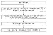
图1是本技术方案第一实施例薄膜晶体管的制备方法流程图。FIG. 1 is a flow chart of a method for manufacturing a thin film transistor according to the first embodiment of the technical solution.
图2是本技术方案第一实施例薄膜晶体管的制备工艺流程图。Fig. 2 is a flow chart of the manufacturing process of the thin film transistor according to the first embodiment of the technical solution.
图3是本技术方案第一实施例碳纳米管层的扫描电镜照片。Fig. 3 is a scanning electron micrograph of the carbon nanotube layer of the first embodiment of the technical solution.
图4是本技术方案第二实施例薄膜晶体管的制备方法流程图。FIG. 4 is a flowchart of a method for manufacturing a thin film transistor according to the second embodiment of the technical solution.
图5是本技术方案第二实施例薄膜晶体管的制备工艺流程图。FIG. 5 is a flow chart of the manufacturing process of the thin film transistor according to the second embodiment of the technical solution.
图6是本技术方案第三实施例薄膜晶体管的制备方法流程图。FIG. 6 is a flowchart of a method for manufacturing a thin film transistor according to the third embodiment of the technical solution.
具体实施方式Detailed ways
以下将结合附图详细说明本技术方案实施例提供的薄膜晶体管的制备方法。The manufacturing method of the thin film transistor provided by the embodiment of the technical solution will be described in detail below with reference to the accompanying drawings.
请参阅图1及图2,本技术方案第一实施例提供一种顶栅型薄膜晶体管10的制备方法,具体包括以下步骤:Please refer to FIG. 1 and FIG. 2. The first embodiment of the technical solution provides a method for manufacturing a top-gate
步骤一:提供一绝缘基底110。Step 1: providing an
所述绝缘基底110为一耐高温基板,其材料不限,只要确保其熔点高于所述碳纳米管的生长温度即可。所述绝缘基底110的形状不限,可为方形、圆形等任何形状。所述绝缘基底110的大小尺寸不限,具体可根据实际情况而定。另外,所述绝缘基底110也可选用大规模集成电路中的基板。The
本技术方案实施例中,所述绝缘基底110为一方形硅基底,该硅基底的长度和宽度均为3厘米。In the embodiment of the technical solution, the
步骤二:形成一碳纳米管层于所述绝缘基底110表面,所述碳纳米管层包括多个碳纳米管,进而形成一半导体层140。Step 2: Form a carbon nanotube layer on the surface of the
所述碳纳米管层可通过以下两种方法形成:其一,在所述绝缘基底110上形成一碳纳米管阵列,以及处理所述碳纳米管阵列,形成一碳纳米管层。其二,直接在所述绝缘基底110表面形成一碳纳米管层。The carbon nanotube layer can be formed by the following two methods: one, forming a carbon nanotube array on the
所述在绝缘基底110上形成一碳纳米管阵列,以及处理所述碳纳米管阵列,形成一碳纳米管层的步骤包括以下步骤:在所述绝缘基底110表面形成一带状催化剂薄膜,该带状催化剂薄膜的宽度为1微米-20微米;采用化学气相沉积法生长一带状碳纳米管阵列;以及处理所述带状碳纳米管阵列,使所述带状碳纳米管阵列沿垂直于其长度的方向倾倒,在绝缘基底110表面形成一碳纳米管层。The step of forming a carbon nanotube array on the
所述带状催化剂薄膜用于生长碳纳米管。该带状催化剂薄膜的材料可选用铁(Fe)、钴(Co)、镍(Ni)或其任意组合的合金之一。本实施例中,所述带状催化剂薄膜的材料为铁。The ribbon-shaped catalyst film is used to grow carbon nanotubes. The material of the belt-shaped catalyst film can be selected from one of iron (Fe), cobalt (Co), nickel (Ni) or any combination thereof. In this embodiment, the material of the strip-shaped catalyst film is iron.
所述带状催化剂薄膜可通过热沉积法、电子束沉积法或溅射法形成于所述绝缘基底110表面。所述带状催化剂薄膜的宽度为1微米-20微米。所述带状催化剂薄膜的厚度为0.1纳米~10纳米。The strip-shaped catalyst film can be formed on the surface of the
所述采用化学气相沉积法生长带状碳纳米管阵列的方法具体包括以下步骤:The method for growing ribbon-shaped carbon nanotube arrays by chemical vapor deposition specifically includes the following steps:
将上述形成有所述带状催化剂薄膜的绝缘基底110放入一反应室中;Put the above-mentioned insulating
通入保护气体,将反应室内的空气排出;Introduce protective gas to discharge the air in the reaction chamber;
在保护气体环境下将反应室加热至600℃~900℃,并保持恒温;Heat the reaction chamber to 600°C-900°C in a protective gas environment and keep it at a constant temperature;
通入流量比为1∶30~1∶3的碳源气及载气,反应5~30分钟,生长碳纳米管;以及Introducing carbon source gas and carrier gas with a flow ratio of 1:30 to 1:3, reacting for 5 to 30 minutes, and growing carbon nanotubes; and
停止通入碳源气,碳纳米管停止生长,同时停止加热,并降温,待降至室温后,将形成有带状碳纳米管阵列的绝缘基底110从反应室中取出。Stop feeding the carbon source gas, stop the growth of carbon nanotubes, stop heating at the same time, and lower the temperature. After cooling down to room temperature, take out the insulating
所述保护气体为氮气或惰性气体。所述碳源气可选用乙醇、乙炔、乙烯等化学性质较活泼的碳氢化合物。所述载气为氢气。通入碳源气的流量为20~200sccm,载气的流量为50~600sccm。在所述停止通入碳源气后,要继续通入保护气体,直到反应室温度降为室温,以防止生长的碳纳米管被氧化。The protective gas is nitrogen or inert gas. The carbon source gas can be selected from hydrocarbons with relatively active chemical properties such as ethanol, acetylene, and ethylene. The carrier gas is hydrogen. The flow rate of the carbon source gas is 20-200 sccm, and the flow rate of the carrier gas is 50-600 sccm. After stopping the feeding of the carbon source gas, continue feeding the protective gas until the temperature of the reaction chamber drops to room temperature, so as to prevent the grown carbon nanotubes from being oxidized.
本实施例中,所述保护气体为氩气,碳源气为乙炔,反应温度为800℃,碳纳米管的生长时间为60分钟。In this embodiment, the protective gas is argon, the carbon source gas is acetylene, the reaction temperature is 800° C., and the growth time of carbon nanotubes is 60 minutes.
另外,可通过调节碳源气和载气的流量比,来控制生长出的碳纳米管的性质,如管径、透明度、电阻等。本技术方案实施例中,当所述碳源气和载气的流量比为1∶100至10∶100时,可生长出单壁碳纳米管。当继续增大碳源气的流量比时,可生长出双壁碳纳米管。故所形成的带状碳纳米管阵列中的碳纳米管可为单壁碳纳米管或双壁碳纳米管。该单壁碳纳米管的直径为0.5纳米~50纳米,该双壁碳纳米管的直径为1.0纳米~50纳米。优选地,所述碳纳米管的直径小于10纳米。In addition, the properties of the grown carbon nanotubes, such as tube diameter, transparency, and electrical resistance, can be controlled by adjusting the flow ratio of carbon source gas and carrier gas. In the embodiment of the technical solution, when the flow ratio of the carbon source gas and the carrier gas is 1:100 to 10:100, single-walled carbon nanotubes can be grown. When the flow ratio of carbon source gas continues to increase, double-walled carbon nanotubes can be grown. Therefore, the carbon nanotubes in the formed ribbon carbon nanotube array can be single-walled carbon nanotubes or double-walled carbon nanotubes. The single-wall carbon nanotube has a diameter of 0.5 nanometers to 50 nanometers, and the double-wall carbon nanotube has a diameter of 1.0 nanometers to 50 nanometers. Preferably, the diameter of the carbon nanotubes is less than 10 nanometers.
在一定条件下,所述带状碳纳米管阵列的生长高度随生长时间的延长而增大。所述带状碳纳米管阵列的生长高度可达1毫米~10毫米。本技术方案实施例中,通入碳源气及载气后反应60分钟,所生长出的带状碳纳米管阵列的高度为1毫米~2毫米。Under certain conditions, the growth height of the ribbon-shaped carbon nanotube array increases with the extension of the growth time. The growth height of the ribbon-shaped carbon nanotube array can reach 1 mm to 10 mm. In the embodiment of the technical solution, after feeding the carbon source gas and the carrier gas and reacting for 60 minutes, the grown strip-shaped carbon nanotube array has a height of 1 mm to 2 mm.
所述带状碳纳米管阵列为由多个长度较长的碳纳米管形成的纯碳纳米管阵列。通过上述控制生长条件,如生长温度,碳源气和载气的流量比等,该带状碳纳米管阵列中的碳纳米管基本不含有杂质,如无定型碳或残留的催化剂金属颗粒等。The strip-shaped carbon nanotube array is a pure carbon nanotube array formed by a plurality of longer carbon nanotubes. By controlling the growth conditions above, such as growth temperature, flow ratio of carbon source gas and carrier gas, etc., the carbon nanotubes in the ribbon-shaped carbon nanotube array basically do not contain impurities, such as amorphous carbon or residual catalyst metal particles.
所述处理所述带状碳纳米管阵列,形成碳纳米管层的步骤可通过以下三种方式实现:其一,采用有机溶剂处理法处理所述带状碳纳米管阵列,形成一碳纳米管层。其二,使用机械外力处理法处理所述带状碳纳米管阵列,形成一碳纳米管层。其三,使用气流处理法处理所述带状碳纳米管阵列,形成一碳纳米管层。The step of processing the strip-shaped carbon nanotube array to form a carbon nanotube layer can be achieved in the following three ways: first, the strip-shaped carbon nanotube array is processed by an organic solvent treatment method to form a carbon nanotube layer. Second, using a mechanical external force treatment method to process the strip-shaped carbon nanotube array to form a carbon nanotube layer. Thirdly, the strip-shaped carbon nanotube array is processed by airflow treatment to form a carbon nanotube layer.
所述采用有机溶剂处理法处理所述碳纳米管阵列,形成一碳纳米管层的方法具体包括以下步骤:提供一盛有有机溶剂的容器;将形成有带状碳纳米管阵列的绝缘基底110浸入盛有有机溶剂的容器中;以及将所述绝缘基底110沿垂直于所述带状碳纳米管阵列的长度方向从有机溶剂中取出,所述碳纳米管阵列在有机溶剂表面张力的作用下倾倒,粘附在所述绝缘基底110表面;使有机溶剂挥发,形成一碳纳米管层。所述有机溶剂可选用挥发性有机溶剂,如乙醇、甲醇、丙酮、二氯乙烷或氯仿,本实施例中采用乙醇。所形成的碳纳米管层在挥发性有机溶剂的表面张力的作用下,可贴附在所述基底表面,且表面体积比减小,粘性降低,具有良好的机械强度及韧性。The method of processing the carbon nanotube array by using an organic solvent treatment method to form a carbon nanotube layer specifically includes the following steps: providing a container filled with an organic solvent; forming an insulating
所述使用机械外力处理法处理所述带状碳纳米管阵列,形成一碳纳米管层的方法具体包括以下步骤:提供一压头;以及将该压头沿垂直于所述带状碳纳米管阵列的长度方向碾压所述带状碳纳米管阵列,碳纳米管沿垂直于所述带状碳纳米管阵列的长度方向倾倒,形成一碳纳米管层。所述压头为滚轴状压头。所述机械外力的施加装置不限于上述压头,也可为一具有一定平整表面的其它装置,只要能使所述带状碳纳米管阵列中的碳纳米管沿垂直于所述带状碳纳米管阵列的长度方向倾倒即可。在压力的作用下,所述带状碳纳米管阵列可与生长的基底分离,从而形成由多个碳纳米管组成的具有自支撑结构的碳纳米管层。The method of processing the ribbon-shaped carbon nanotube array by using mechanical external force treatment method to form a carbon nanotube layer specifically includes the following steps: providing an indenter; Rolling the strip-shaped carbon nanotube array along the length direction of the array, the carbon nanotubes are poured along the length direction perpendicular to the strip-shaped carbon nanotube array to form a carbon nanotube layer. The indenter is a roller-shaped indenter. The device for applying external mechanical force is not limited to the above-mentioned indenter, and can also be other devices with a certain flat surface, as long as the carbon nanotubes in the ribbon-shaped carbon nanotube array can be perpendicular to the ribbon-shaped carbon nanotubes. The length direction of the tube array can be poured. Under the action of pressure, the strip-shaped carbon nanotube array can be separated from the growing substrate, thereby forming a self-supporting carbon nanotube layer composed of a plurality of carbon nanotubes.
所述使用气流处理法处理所述带状碳纳米管阵列,形成一碳纳米管层的方法具体包括以下步骤:提供一风机,该风机可产生一气流;以及将该风机沿垂直于所述带状碳纳米管阵列的长度方向施加一气流于所述带状碳纳米管阵列,碳纳米管沿垂直于所述带状碳纳米管阵列的长度方向倾倒,形成一碳纳米管层。所述气流的施加装置不限于上述风机,可为任何可产生气流的装置。The method for processing the strip-shaped carbon nanotube array by using the air flow treatment method to form a carbon nanotube layer specifically includes the following steps: providing a fan, which can generate an air flow; A gas flow is applied to the strip-shaped carbon nanotube array in the length direction of the strip-shaped carbon nanotube array, and the carbon nanotubes are poured along the length direction perpendicular to the strip-shaped carbon nanotube array to form a carbon nanotube layer. The device for applying the air flow is not limited to the fan mentioned above, but can be any device that can generate air flow.
本实施例中,所述碳纳米管层的密度与上述带状催化剂薄膜的宽度有关。所述带状催化剂薄膜的宽度越大,所制备的碳纳米管层的密度则越大;反之,所述带状催化剂薄膜的宽度越小,所制备的碳纳米管层的密度则越小。可以理解,通过控制带状催化剂薄膜的宽度,即可控制所制备的碳纳米管层的密度。In this embodiment, the density of the carbon nanotube layer is related to the width of the strip-shaped catalyst film. The larger the width of the strip-shaped catalyst film, the greater the density of the prepared carbon nanotube layer; conversely, the smaller the width of the strip-shaped catalyst film, the smaller the density of the prepared carbon nanotube layer. It can be understood that by controlling the width of the strip-shaped catalyst film, the density of the prepared carbon nanotube layer can be controlled.
可以理解,由于上述碳纳米管的生长温度较高,因此,上述绝缘基底110的材料必须选用耐高温的硬性材料,从而限制了基底材料的选择。为使该薄膜晶体管10能够采用更广泛的基底材料,尤其为一柔性基底材料,从而形成一柔性薄膜晶体管10,在生长碳纳米管层后可以进一步通过一转印步骤,将该碳纳米管层转印在其它基底上。具体地,该转印步骤包括以下步骤:首先,提供一转印基底;其次,将该形成有碳纳米管层的绝缘基底110倒扣在该转印基底上,使碳纳米管层表面与转印基底表面接触,从而形成一从上到下依次包括绝缘基底110、碳纳米管层以及转印基底的三层结构;再次,热压该三层结构;最后,移去绝缘基底110,从而使上述碳纳米管层黏附于转印基底表面。It can be understood that, due to the high growth temperature of the above-mentioned carbon nanotubes, the material of the above-mentioned insulating
该转印基底的材料为一柔性材料,如塑料或树脂材料等。本实施例中,该转印基底为一PET薄膜。热压的温度及时间取决于转印基底的材料种类。当该转印基底的材料为一塑料或树脂时,热压温度为50~200℃,热压时间为5~30分钟。通过热压步骤,碳纳米管与转印基底表面的结合更为紧密,从而能够容易地与绝缘基底110分离。The material of the transfer base is a flexible material, such as plastic or resin material. In this embodiment, the transfer substrate is a PET film. The temperature and time of hot pressing depend on the material type of the transfer substrate. When the material of the transfer base is a plastic or resin, the hot pressing temperature is 50-200° C., and the hot pressing time is 5-30 minutes. Through the hot pressing step, the carbon nanotubes are more tightly bonded to the surface of the transfer substrate, so that they can be easily separated from the insulating
请参见图3,所制备的碳纳米管层包括多个择优取向排列的碳纳米管。所述碳纳米管层中的多个碳纳米管具有大致相等的长度。优选地,所述碳纳米管层中的多个碳纳米管相互平行。Please refer to FIG. 3 , the prepared carbon nanotube layer includes a plurality of carbon nanotubes arranged in preferred orientations. The plurality of carbon nanotubes in the carbon nanotube layer have approximately equal lengths. Preferably, a plurality of carbon nanotubes in the carbon nanotube layer are parallel to each other.
所述直接在绝缘基底110表面形成一碳纳米管层的步骤具体包括以下步骤:提供一生长基底,该生长基底表面形成有一单分散性催化剂层;将所述生长基底和绝缘基底110放入一反应室中,且使所述生长基底和绝缘基底110间隔设置,在保护气体环境下加热到碳纳米管的生长温度,通入碳源气,沿着气流的方向生长碳纳米管,在所述绝缘基底110表面形成一碳纳米管薄膜,进而形成一碳纳米管层。The step of directly forming a carbon nanotube layer on the surface of the insulating
所述催化剂的材料可为铁、钴、镍或其任意组合的合金材料,或金属盐的单分散性溶液或者金属的单分散性溶液。当选用铁、钴、镍或其任意组合的合金材料制备单分散性催化剂层时,可采用沉积方法将催化剂材料沉积到生长基底表面;当选用金属盐的单分散性溶液或者金属的单分散性溶液制备单分散性催化剂层,可将金属盐或者金属的单分散性溶液涂敷于生长基底上,烘干后即形成所述催化剂层。The material of the catalyst can be iron, cobalt, nickel or an alloy material in any combination thereof, or a monodisperse solution of a metal salt or a monodisperse solution of a metal. When iron, cobalt, nickel or alloy materials in any combination thereof are used to prepare a monodisperse catalyst layer, the catalyst material can be deposited on the surface of the growth substrate by a deposition method; when a monodisperse solution of a metal salt or a monodisperse metal To prepare a monodisperse catalyst layer from a solution, the metal salt or metal monodisperse solution can be coated on the growth substrate, and the catalyst layer can be formed after drying.
所述生长基底为一耐高温基板,其材料不限,只要确保其熔点高于所述碳纳米管的生长温度即可。所述基底形状不限,可为方形、圆形等任何形状。本技术方案实施例所述生长基底采用与所述绝缘基底110同样材料,同样尺寸的基底。The growth substrate is a high temperature resistant substrate, and its material is not limited, as long as its melting point is higher than the growth temperature of the carbon nanotubes. The shape of the base is not limited, it can be any shape such as square, circle, etc. The growth substrate in the embodiment of the technical solution is made of the same material and size as the insulating
所述碳纳米管的生长温度为800℃~1000℃。当通入碳源气后,在生长基底表面催化剂颗粒的作用下开始生长碳纳米管。碳纳米管一端固定于生长基底上,另一端不断生长。由于催化剂层包括多个单分散性催化剂颗粒,所以生长的碳纳米管不会很密,从而使得部分碳纳米管可以长成为长度较长的碳纳米管。将所述碳源气从靠近生长基底处通入,所以随着碳源气的不断通入,生长的碳纳米管随着碳源气漂浮于绝缘基底110上空。该生长机理称作“放风筝机理”。碳纳米管的生长时间与所要制备的碳纳米管的长度有关。本实施例中,生长时间为30分钟时,所生长出的碳纳米管的长度可达8厘米。当停止通入碳源气,碳纳米管停止生长,平行且间隔的形成于绝缘基底110上,形成一碳纳米管薄膜。该碳纳米管薄膜中相邻两个碳纳米管之间的距离大于20微米。The growth temperature of the carbon nanotubes is 800°C to 1000°C. After the carbon source gas is introduced, carbon nanotubes begin to grow under the action of catalyst particles on the surface of the growth substrate. One end of the carbon nanotube is fixed on the growth substrate, and the other end is continuously growing. Since the catalyst layer includes a plurality of monodisperse catalyst particles, the grown carbon nanotubes will not be very dense, so that some carbon nanotubes can grow into longer carbon nanotubes. The carbon source gas is introduced from a place close to the growth substrate, so as the carbon source gas is continuously introduced, the grown carbon nanotubes float above the insulating
进一步地,为了提高所生长出的碳纳米管薄膜中碳纳米管的密度,可通过更换新的生长基底或将原生长基底取出清洗后沉积新的催化剂薄膜的方式来实现碳纳米管的多次生长,形成多个碳纳米管薄膜,进而提高所生长出的碳纳米管薄膜的密度,所述多个碳纳米管薄膜形成一碳纳米管层。另外,在上述碳纳米管的多次生长中,也可将所述绝缘基底110旋转一定角度,从而使相邻两层碳纳米管薄膜的碳纳米管之间具有一交叉角度α,α大于等于0度且小于等于90度。所述碳纳米管层包括多个碳纳米管,且碳纳米管之间通过范德华力紧密结合形成一自支撑结构。Further, in order to increase the density of carbon nanotubes in the grown carbon nanotube film, carbon nanotubes can be regenerated multiple times by replacing the new growth substrate or taking out the original growth substrate for cleaning and depositing a new catalyst film. grow to form a plurality of carbon nanotube films, and then increase the density of the grown carbon nanotube films, and the plurality of carbon nanotube films form a carbon nanotube layer. In addition, in the multiple growth of the above-mentioned carbon nanotubes, the insulating
另外,当所制备的碳纳米管层的面积较大时,或当需要制备多个薄膜晶体管10时,可将所形成的碳纳米管层刻蚀成多个具有所需形状和尺寸的碳纳米管层,该碳纳米管层用作半导体层140。所述刻蚀方法不限,可为现有技术中任何刻蚀方法。In addition, when the area of the prepared carbon nanotube layer is large, or when it is necessary to prepare a plurality of
步骤三:间隔形成一源极151及一漏极152,并使该源极151及漏极152与上述半导体层140中的部分碳纳米管的两端电连接。Step 3: Forming a
该源极151及漏极152的材料应具有较好的导电性。具体地,该源极151及漏极152的材料可以为金属、合金、铟锡氧化物(ITO)、锑锡氧化物(ATO)、导电银胶、导电聚合物以及碳纳米管薄膜等导电材料。根据形成源极151及漏极152的材料种类的不同,可以采用不同方法形成该源极151及漏极152。具体地,当该源极151及漏极152的材料为金属、合金、ITO或ATO时,可以通过蒸镀、溅射、沉积、掩模及刻蚀等方法形成源极151及漏极152。当该源极151及漏极152的材料为导电银胶、导电聚合物或碳纳米管薄膜时,可以通过直接黏附或印刷涂附的方法,将该导电银胶或碳纳米管薄膜涂附或黏附于绝缘基底110或半导体层140表面,形成源极151及漏极152。一般地,该源极151及漏极152的厚度为0.5纳米~100微米,源极151至漏极152之间的距离为1~100微米。The material of the
本实施例中,该源极151及漏极152的材料为金属。上述步骤三具体可通过下述两种方式进行。第一种方式具体包括以下步骤:首先,在上述半导体层140表面均匀涂覆一层光刻胶;其次,通过曝光及显影等光刻方法在光刻胶上形成源极151及漏极152区域,在该源极151及漏极152区域露出该半导体层140;再次,通过真空蒸镀、磁控溅射或电子束蒸发沉积等沉积方法在上述光刻胶、源极151及漏极152区域表面沉积一金属层,优选为钯、钛或镍金属层;最后,通过丙酮等有机溶剂去除光刻胶及其上的金属层,即得到形成在半导体层140上的源极151及漏极152。第二种方式具体包括以下步骤:首先,在半导体层140表面沉积一金属层;其次,在该金属层表面涂覆一层光刻胶;再次,通过曝光及显影等光刻方法去除源极151区域及漏极152区域外的光刻胶;最后,通过等离子体刻蚀等方法去除源极151区域及漏极152区域外的金属层,并以丙酮等有机溶剂去除源极151区域及漏极152区域上的光刻胶,即得到形成在半导体层140上的源极151及漏极152。本实施例中,该源极151及漏极152的厚度为1微米,源极151至漏极152之间的距离为50微米。In this embodiment, the material of the
可以理解,为了得到具有更好的半导体性的半导体层140,在形成源极151及漏极152之后,可以进一步包括一去除半导体层140中的导体性碳纳米管的步骤。具体包括以下步骤:首先,提供一外部电源,其次,将外部电源的正负两极连接至源极151及漏极152;最后,通过外部电源在源极151及漏极152两端施加一较大电压,使导体性的碳纳米管发热并烧蚀,获得一半导体性的半导体层140。该电压在1~1000伏范围内。It can be understood that, in order to obtain the
另外,上述去除半导体层140中导体性碳纳米管的方法也可以使用氢等离子体、微波、太赫兹(THz)、红外线(IR)、紫外线(UV)或可见光(Vis)照射该半导体层140,使导体性碳纳米管发热并烧蚀,获得一半导体性的半导体层140。In addition, the method for removing the conductive carbon nanotubes in the
步骤四:在上述半导体层140上形成一绝缘层130。Step 4: forming an insulating
该绝缘层130的材料可以为氮化硅、氧化硅等硬性材料或苯并环丁烯(BCB)、聚酯或丙烯酸树脂等柔性材料。根据绝缘层130的材料种类的不同,可以采用不同方法形成该绝缘层130。具体地,当该绝缘层130的材料为氮化硅或氧化硅时,可以通过沉积的方法形成绝缘层130。当该绝缘层130的材料为苯并环丁烯(BCB)、聚酯或丙烯酸树脂时,可以通过印刷涂附的方法形成绝缘层130。一般地,该绝缘层130的厚度为0.5纳米~100微米。The insulating
本实施方式中采用等离子体化学气相沉积等沉积方法形成一氮化硅绝缘层130覆盖于半导体层140及形成在半导体层140上的源极151及漏极152表面。所述绝缘层130的厚度约为1微米。In this embodiment, a deposition method such as plasma chemical vapor deposition is used to form a silicon
可以理解,根据薄膜晶体管10的不同应用,可以采用与形成源极151及漏极152相似的光刻或刻蚀的方法将所述源极151及漏极152的一部分暴露在绝缘层130外。It can be understood that, according to different applications of the
步骤五:形成一栅极120于所述绝缘层130表面,得到一薄膜晶体管10。Step 5: forming a
该栅极120的材料应具有较好的导电性。具体地,该栅极120的材料可以为金属、合金、ITO、ATO、导电银胶、导电聚合物以及碳纳米管薄膜等导电材料。该金属或合金材料可以为铝、铜、钨、钼、金或它们的合金。具体地,当该栅极120的材料为金属、合金、ITO或ATO时,可以通过蒸镀、溅射、沉积、掩模及刻蚀等方法形成栅极120。当该栅极120的材料为导电银胶、导电聚合物或碳纳米管薄膜时,可以通过直接黏附或印刷涂附的方法形成栅极120。一般地,该栅极120的厚度为0.5纳米~100微米。The material of the
本技术方案实施例中通过与形成源极151及漏极152相似的方法在绝缘层130表面且与半导体层140相对的位置形成一导电薄膜作为栅极120。该栅极120通过绝缘层130与半导体层140电绝缘。本技术方案实施例中,所述栅极120的材料为钯,栅极120的厚度约为1微米。In the embodiment of the technical solution, a conductive thin film is formed as the
请参阅图4及图5,本技术方案第二实施例提供一种底栅型薄膜晶体管20的制备方法,其与第一实施例中薄膜晶体管10的制备方法基本相同。主要区别在于,本实施例中形成的薄膜晶体管20为一底栅型结构。本技术方案第二实施例薄膜晶体管20的制备方法包括以下步骤:Referring to FIG. 4 and FIG. 5 , the second embodiment of the technical solution provides a method for manufacturing a bottom-gate
步骤一:提供一生长基底。Step 1: providing a growth substrate.
步骤二:形成一碳纳米管层于所述生长基底表面,所述碳纳米管层包括多个碳纳米管。Step 2: forming a carbon nanotube layer on the surface of the growth substrate, the carbon nanotube layer including a plurality of carbon nanotubes.
步骤三:提供一绝缘基底210。Step 3: Provide an insulating
步骤四:形成一栅极220于所述绝缘基底210表面。Step 4: forming a
步骤五:形成一绝缘层230覆盖所述栅极220。Step 5: forming an insulating
步骤六:转印该碳纳米管层至所述绝缘层230表面,形成一半导体层240。Step 6: transfer the carbon nanotube layer to the surface of the insulating
该转印步骤具体包括以下步骤:首先,将该形成有碳纳米管层的生长基底倒扣在绝缘基底210上使碳纳米管层表面与绝缘层230表面接触,从而形成一从上到下依次包括生长基底、碳纳米管层以及绝缘基底210的三层结构;再次,热压该三层结构;最后,移去生长基底,从而使上述碳纳米管层黏附于所述绝缘层230表面,形成一半导体层240。The transfer step specifically includes the following steps: First, the growth substrate formed with the carbon nanotube layer is turned upside down on the insulating
当将该形成有碳纳米管层的生长基底倒扣在绝缘基底210上时,应确保该碳纳米管层表面与绝缘层230表面相贴合,从而使碳纳米管层黏附在绝缘层230上。When the growth substrate formed with the carbon nanotube layer is buckled upside down on the insulating
步骤七:间隔形成一源极251及一漏极252,并使该源极251及漏极252与上述半导体层240中的部分碳纳米管的两端电连接。Step 7: Forming a
所述源极251、漏极252、栅极220及绝缘层230均可采用与第一实施例相同的方法形成。The
请参阅图6,本技术方案第三实施例提供一种薄膜晶体管的制备方法,其与第一实施例薄膜晶体管10的制备方法基本相同。主要区别在于,本实施例在同一绝缘基底上形成多个薄膜晶体管,从而形成一薄膜晶体管阵列。本实施例薄膜晶体管的制备方法具体包括以下步骤:Please refer to FIG. 6 , the third embodiment of the technical solution provides a method for manufacturing a thin film transistor, which is basically the same as the method for manufacturing the
步骤一:提供一绝缘基底。Step 1: providing an insulating base.
步骤二:在绝缘基底表面均匀形成多个碳纳米管层,所述碳纳米管层包括多个碳纳米管,进而形成多个半导体层。Step 2: uniformly forming a plurality of carbon nanotube layers on the surface of the insulating substrate, the carbon nanotube layer including a plurality of carbon nanotubes, and then forming a plurality of semiconductor layers.
上述步骤二可通过两种方式进行。第一种方式具体包括以下步骤:在绝缘基底表面形成一大面积的碳纳米管层;以及采用掩模及刻蚀等方法图案化该碳纳米管层,从而在需要形成薄膜晶体管的不同位置形成多个碳纳米管层。第二种方式具体包括以下步骤:在预形成薄膜晶体管的位置形成多个带状催化剂薄膜;采用化学气相沉积法生长多个带状碳纳米管阵列;以及对多个带状碳纳米管阵列进行处理,形成多个碳纳米管层。The above step 2 can be carried out in two ways. The first method specifically includes the following steps: forming a large-area carbon nanotube layer on the surface of an insulating substrate; and patterning the carbon nanotube layer by using methods such as masking and etching, so as to form Multiple carbon nanotube layers. The second method specifically includes the following steps: forming a plurality of strip-shaped catalyst thin films at the positions of the pre-formed thin film transistors; growing a plurality of strip-shaped carbon nanotube arrays by chemical vapor deposition; processing to form multiple carbon nanotube layers.
当所述多个带状催化剂薄膜可通过热沉积法、电子束沉积法或溅射法多次沉积而形成,也可通过光刻法或掩模法来实现。所述带状催化剂薄膜之间的间距优选为10微米-15毫米。所述带状催化剂薄膜的宽度为1微米-20微米。所述带状催化剂薄膜的厚度为0.1纳米~10纳米。When the plurality of belt-shaped catalyst thin films can be formed by thermal deposition, electron beam deposition or sputtering, they can also be formed by photolithography or masking. The distance between the strip-shaped catalyst films is preferably 10 micrometers to 15 millimeters. The width of the strip-shaped catalyst film is 1 micron-20 microns. The thickness of the strip-shaped catalyst film is 0.1 nanometers to 10 nanometers.
步骤四:间隔形成多个源极及多个漏极,并使上述每一半导体层中的部分碳纳米管的两端均与一源极及一漏极电连接。Step 4: Forming a plurality of sources and drains at intervals, and electrically connecting both ends of some carbon nanotubes in each semiconductor layer to a source and a drain.
与本技术方案第一实施例中的源极151及漏极152的形成方法相似,可以先在形成有多个半导体层的整个绝缘基底表面沉积一金属薄膜,再通过刻蚀等方法图案化该金属薄膜,从而在预定位置上一次形成多个源极及多个漏极。上述源极及漏极的材料也可为ITO、ATO、导电聚合物、导电银胶或碳纳米管。Similar to the method for forming the
步骤五:形成一绝缘层于每一半导体层表面。Step 5: forming an insulating layer on the surface of each semiconductor layer.
上述绝缘层的形成方法与本技术方案第一实施例中的薄膜晶体管10中的绝缘层130的制备方法相似,可以先在整个绝缘基底的表面沉积一氮化硅薄膜,再通过刻蚀等方法图案化该氮化硅薄膜,从而在预定位置上一次形成多个绝缘层。上述绝缘层的材料也可为氧化硅等硬性材料或苯并环丁烯(BCB)、聚酯或丙烯酸树脂等柔性材料。The method for forming the above-mentioned insulating layer is similar to the method for preparing the insulating
步骤六:形成一栅极于每一绝缘层表面,得到多个薄膜晶体管。Step 6: forming a gate on the surface of each insulating layer to obtain a plurality of thin film transistors.
可以理解,通过与第二实施例相似的方法,也可以形成多个薄膜晶体管,进而形成一薄膜晶体管阵列,其具体包括以下步骤:It can be understood that a plurality of thin film transistors can also be formed by a method similar to that of the second embodiment, thereby forming a thin film transistor array, which specifically includes the following steps:
步骤一:提供一生长基底。Step 1: providing a growth substrate.
步骤二:形成一碳纳米管层于所述生长基底表面,所述碳纳米管层包括多个碳纳米管。Step 2: forming a carbon nanotube layer on the surface of the growth substrate, the carbon nanotube layer including a plurality of carbon nanotubes.
步骤三:提供一绝缘基底。Step 3: providing an insulating base.
步骤四:形成多个栅极于所述绝缘基底表面。Step 4: forming a plurality of gates on the surface of the insulating substrate.
步骤五:形成至少一绝缘层覆盖所述多个栅极。Step 5: forming at least one insulating layer to cover the plurality of gates.
步骤六:铺设上述至少一碳纳米管层于所述绝缘层表面,图案化该碳纳米管层,形成多个半导体层,该多个半导体层与上述多个栅极通过绝缘层相对并绝缘设置。Step 6: laying the above-mentioned at least one carbon nanotube layer on the surface of the insulating layer, patterning the carbon nanotube layer to form a plurality of semiconductor layers, and the plurality of semiconductor layers are opposite to the above-mentioned plurality of gates through the insulating layer and are insulated. .
步骤七:间隔形成多个源极及多个漏极,并使该源极及漏极与上述半导体层中的部分碳纳米管的两端电连接,形成多个薄膜晶体管。Step 7: Forming a plurality of sources and drains at intervals, and electrically connecting the sources and drains to the two ends of some carbon nanotubes in the semiconductor layer to form a plurality of thin film transistors.
本技术方案实施例薄膜晶体管的制备方法具有以下优点:其一,由于所述半导体层可直接形成在所述绝缘基底上,或通过对形成在所述生长基底上的碳纳米管阵列进行转印处理而制备,这种半导体层的形成方法比现有技术中的喷墨打印法形成薄膜晶体管半导体层的方法简单,无需经过在有机溶剂中分散碳纳米管的步骤。其二,由于所制备的碳纳米管层中的碳纳米管沿一定方向平行排列,因此,将该碳纳米管层作为半导体层时,可以通过控制碳纳米管层的设置方向来控制源极至漏极间碳纳米管的排列方向,从而使薄膜晶体管获得较大的载流子迁移率。其三,由于碳纳米管具有优异的力学性能,则由多个择优取向排列或具有一定交叉角度的碳纳米管组成的半导体层具有较好的韧性及机械强度,从而有利于制备柔性薄膜晶体管。其四,可通过对所制备的大面积碳纳米管层进行刻蚀或制备多个碳纳米管层来制备多个薄膜晶体管,进而可实现薄膜晶体管的批量生产,且该方法制备的薄膜晶体管的成本较低。其五,由于本实施例所提供的碳纳米管层可以采用一转印步骤将碳纳米管层转印到其它基底上,该基底的材料可以选择不耐高温的柔性材料,有利于制备柔性薄膜晶体管。The preparation method of the thin film transistor in the embodiment of the technical solution has the following advantages: First, since the semiconductor layer can be directly formed on the insulating substrate, or by transferring the carbon nanotube array formed on the growth substrate The semiconductor layer is prepared by processing, and the method for forming the semiconductor layer is simpler than the inkjet printing method in the prior art for forming the semiconductor layer of the thin film transistor, without the step of dispersing carbon nanotubes in an organic solvent. Second, since the carbon nanotubes in the prepared carbon nanotube layer are arranged in parallel along a certain direction, when the carbon nanotube layer is used as a semiconductor layer, the source electrode to the The alignment direction of the carbon nanotubes between the drains enables the thin film transistor to obtain greater carrier mobility. Third, due to the excellent mechanical properties of carbon nanotubes, the semiconductor layer composed of multiple carbon nanotubes arranged in preferred orientations or with a certain crossing angle has good toughness and mechanical strength, which is conducive to the preparation of flexible thin film transistors. Fourth, multiple thin-film transistors can be prepared by etching the prepared large-area carbon nanotube layer or preparing multiple carbon nanotube layers, and then mass production of thin-film transistors can be realized, and the thin-film transistors prepared by this method have The cost is lower. Fifth, since the carbon nanotube layer provided in this embodiment can adopt a transfer printing step to transfer the carbon nanotube layer to other substrates, the material of the substrate can be selected from flexible materials that are not resistant to high temperatures, which is conducive to the preparation of flexible films transistor.
另外,本领域技术人员还可在本发明精神内作其它变化,当然这些依据本发明精神所作的变化,都应包含在本发明所要求保护的范围内。In addition, those skilled in the art can also make other changes within the spirit of the present invention. Of course, these changes made according to the spirit of the present invention should be included in the scope of protection claimed by the present invention.
Claims (14)
Translated fromChinesePriority Applications (5)
| Application Number | Priority Date | Filing Date | Title |
|---|---|---|---|
| CN2008100674259ACN101587839B (en) | 2008-05-23 | 2008-05-23 | Method for producing thin film transistors |
| US12/384,241US8597990B2 (en) | 2008-05-23 | 2009-04-02 | Method for making thin film transistor |
| EP09160164.1AEP2120274B1 (en) | 2008-05-14 | 2009-05-13 | Carbon Nanotube Thin Film Transistor |
| JP2009125627AJP5193946B2 (en) | 2008-05-23 | 2009-05-25 | Thin film transistor manufacturing method |
| US14/059,753US9153667B2 (en) | 2008-05-23 | 2013-10-22 | Method for making thin film transistor |
Applications Claiming Priority (1)
| Application Number | Priority Date | Filing Date | Title |
|---|---|---|---|
| CN2008100674259ACN101587839B (en) | 2008-05-23 | 2008-05-23 | Method for producing thin film transistors |
Publications (2)
| Publication Number | Publication Date |
|---|---|
| CN101587839A CN101587839A (en) | 2009-11-25 |
| CN101587839Btrue CN101587839B (en) | 2011-12-21 |
Family
ID=41342425
Family Applications (1)
| Application Number | Title | Priority Date | Filing Date |
|---|---|---|---|
| CN2008100674259AActiveCN101587839B (en) | 2008-05-14 | 2008-05-23 | Method for producing thin film transistors |
Country Status (3)
| Country | Link |
|---|---|
| US (2) | US8597990B2 (en) |
| JP (1) | JP5193946B2 (en) |
| CN (1) | CN101587839B (en) |
Families Citing this family (15)
| Publication number | Priority date | Publication date | Assignee | Title |
|---|---|---|---|---|
| CN101604603B (en)* | 2008-06-13 | 2011-03-23 | 清华大学 | Filed emission body and preparation method thereof |
| CN102050424B (en)* | 2009-11-06 | 2013-11-06 | 清华大学 | Method for preparing carbon nanotube thin film and method for preparing thin film transistor |
| CN101880035A (en) | 2010-06-29 | 2010-11-10 | 清华大学 | carbon nanotube structure |
| US8193032B2 (en) | 2010-06-29 | 2012-06-05 | International Business Machines Corporation | Ultrathin spacer formation for carbon-based FET |
| US9024310B2 (en)* | 2011-01-12 | 2015-05-05 | Tsinghua University | Epitaxial structure |
| JP2012212796A (en)* | 2011-03-31 | 2012-11-01 | National Institute Of Advanced Industrial & Technology | Manufacturing method of microstructure, microstructure manufactured by manufacturing method thereof, and field effect semiconductor element having microstructure |
| US8916405B2 (en)* | 2011-10-11 | 2014-12-23 | International Business Machines Corporation | Light emitting diode (LED) using carbon materials |
| CN104507685B (en)* | 2012-08-06 | 2017-06-09 | 株式会社尼康 | Transfer device and substrate processing device |
| US10475594B2 (en)* | 2014-04-22 | 2019-11-12 | Nexdot | Electronic device comprising nanogap electrodes and nanoparticle |
| CN105097428B (en)* | 2014-04-24 | 2017-12-01 | 清华大学 | Carbon nano-tube compound film |
| CN103940269B (en)* | 2014-04-25 | 2017-04-26 | 上海交通大学 | Heat tube based on carbon nano tube wick and manufacturing method of heat tube |
| US20180175297A1 (en)* | 2014-12-09 | 2018-06-21 | University Of Southern California | Screen Printing Systems and Techniques for Creating Thin-Film Transistors Using Separated Carbon Nanotubes |
| US9704969B1 (en)* | 2015-12-31 | 2017-07-11 | Taiwan Semiconductor Manufacturing Co., Ltd. | Fin semiconductor device having multiple gate width structures |
| CN107564946A (en)* | 2016-07-01 | 2018-01-09 | 清华大学 | nano-transistor |
| JP7264349B2 (en)* | 2017-02-28 | 2023-04-25 | 国立大学法人東京工業大学 | Carbon film and terahertz wave detection device suitable for light receiving element and power feeding element using terahertz wave |
Citations (1)
| Publication number | Priority date | Publication date | Assignee | Title |
|---|---|---|---|---|
| CN1745468A (en)* | 2002-09-30 | 2006-03-08 | 纳米系统公司 | Large-area nanoenabled macroelectronic substrates and uses therefor |
Family Cites Families (84)
| Publication number | Priority date | Publication date | Assignee | Title |
|---|---|---|---|---|
| JP3318285B2 (en)* | 1999-05-10 | 2002-08-26 | 松下電器産業株式会社 | Method for manufacturing thin film transistor |
| US6423583B1 (en) | 2001-01-03 | 2002-07-23 | International Business Machines Corporation | Methodology for electrically induced selective breakdown of nanotubes |
| US7084507B2 (en)* | 2001-05-02 | 2006-08-01 | Fujitsu Limited | Integrated circuit device and method of producing the same |
| JP4207398B2 (en) | 2001-05-21 | 2009-01-14 | 富士ゼロックス株式会社 | Method for manufacturing wiring of carbon nanotube structure, wiring of carbon nanotube structure, and carbon nanotube device using the same |
| US6814832B2 (en)* | 2001-07-24 | 2004-11-09 | Seiko Epson Corporation | Method for transferring element, method for producing element, integrated circuit, circuit board, electro-optical device, IC card, and electronic appliance |
| US20050279987A1 (en)* | 2002-09-05 | 2005-12-22 | Alexander Star | Nanostructure sensor device with polymer recognition layer |
| US6899945B2 (en)* | 2002-03-19 | 2005-05-31 | William Marsh Rice University | Entangled single-wall carbon nanotube solid material and methods for making same |
| CN100411979C (en)* | 2002-09-16 | 2008-08-20 | 清华大学 | A carbon nanotube rope and its manufacturing method |
| WO2004032193A2 (en) | 2002-09-30 | 2004-04-15 | Nanosys, Inc. | Large-area nanoenabled macroelectronic substrates and uses therefor |
| US7135728B2 (en)* | 2002-09-30 | 2006-11-14 | Nanosys, Inc. | Large-area nanoenabled macroelectronic substrates and uses therefor |
| US7051945B2 (en)* | 2002-09-30 | 2006-05-30 | Nanosys, Inc | Applications of nano-enabled large area macroelectronic substrates incorporating nanowires and nanowire composites |
| US7067867B2 (en)* | 2002-09-30 | 2006-06-27 | Nanosys, Inc. | Large-area nonenabled macroelectronic substrates and uses therefor |
| CN1208818C (en) | 2002-10-16 | 2005-06-29 | 中国科学院化学研究所 | A kind of preparation method of arrayed carbon nanotube thin film transistor |
| WO2004053464A1 (en)* | 2002-12-09 | 2004-06-24 | Rensselaer Polytechnic Institute | Embedded nanotube array sensor and method of making a nanotube polymer composite |
| US7359888B2 (en)* | 2003-01-31 | 2008-04-15 | Hewlett-Packard Development Company, L.P. | Molecular-junction-nanowire-crossbar-based neural network |
| US7150865B2 (en) | 2003-03-31 | 2006-12-19 | Honda Giken Kogyo Kabushiki Kaisha | Method for selective enrichment of carbon nanotubes |
| JP4586334B2 (en)* | 2003-05-07 | 2010-11-24 | ソニー株式会社 | Field effect transistor and manufacturing method thereof |
| CN100533770C (en) | 2003-07-17 | 2009-08-26 | 松下电器产业株式会社 | Field-effect transistor and its manufacturing method |
| US20050061496A1 (en) | 2003-09-24 | 2005-03-24 | Matabayas James Christopher | Thermal interface material with aligned carbon nanotubes |
| US7399400B2 (en)* | 2003-09-30 | 2008-07-15 | Nano-Proprietary, Inc. | Nanobiosensor and carbon nanotube thin film transistors |
| US6921684B2 (en) | 2003-10-17 | 2005-07-26 | Intel Corporation | Method of sorting carbon nanotubes including protecting metallic nanotubes and removing the semiconducting nanotubes |
| US7746418B2 (en)* | 2003-10-30 | 2010-06-29 | Panasonic Corporation | Conductive thin film and thin film transistor |
| CN100592545C (en) | 2003-10-30 | 2010-02-24 | 松下电器产业株式会社 | Conductive Thin Films and Thin Film Transistors |
| KR20050068207A (en)* | 2003-12-29 | 2005-07-05 | 엘지.필립스 엘시디 주식회사 | Laser mask having 2-block and method of crystallization using thereof |
| JP4124787B2 (en)* | 2004-01-15 | 2008-07-23 | 松下電器産業株式会社 | Field effect transistor and display device using the same |
| TWI231153B (en) | 2004-02-26 | 2005-04-11 | Toppoly Optoelectronics Corp | Organic electroluminescence display device and its fabrication method |
| US7253431B2 (en)* | 2004-03-02 | 2007-08-07 | International Business Machines Corporation | Method and apparatus for solution processed doping of carbon nanotube |
| US7330369B2 (en)* | 2004-04-06 | 2008-02-12 | Bao Tran | NANO-electronic memory array |
| US8158203B2 (en)* | 2004-05-06 | 2012-04-17 | William Marsh Rice University | Methods of attaching or grafting carbon nanotubes to silicon surfaces and composite structures derived therefrom |
| TWI240904B (en) | 2004-05-28 | 2005-10-01 | Quanta Display Inc | LCD with improved gray-scale display |
| US7323730B2 (en)* | 2004-07-21 | 2008-01-29 | Commissariat A L'energie Atomique | Optically-configurable nanotube or nanowire semiconductor device |
| US7129097B2 (en)* | 2004-07-29 | 2006-10-31 | International Business Machines Corporation | Integrated circuit chip utilizing oriented carbon nanotube conductive layers |
| KR101025846B1 (en)* | 2004-09-13 | 2011-03-30 | 삼성전자주식회사 | Transistors in Semiconductor Devices Containing Carbon Nanotube Channels |
| US7285501B2 (en)* | 2004-09-17 | 2007-10-23 | Hewlett-Packard Development Company, L.P. | Method of forming a solution processed device |
| TWI307958B (en) | 2004-10-29 | 2009-03-21 | Hon Hai Prec Ind Co Ltd | Field effect transistor |
| JP2008520540A (en)* | 2004-11-17 | 2008-06-19 | ハイピリオン カタリシス インターナショナル インコーポレイテッド | Preparation of catalyst support and supported catalyst from single-walled carbon nanotubes |
| JP5028744B2 (en) | 2005-02-15 | 2012-09-19 | 富士通株式会社 | Method for forming carbon nanotube and method for manufacturing electronic device |
| US20060188721A1 (en) | 2005-02-22 | 2006-08-24 | Eastman Kodak Company | Adhesive transfer method of carbon nanotube layer |
| US20060194058A1 (en) | 2005-02-25 | 2006-08-31 | Amlani Islamshah S | Uniform single walled carbon nanotube network |
| JP4636921B2 (en)* | 2005-03-30 | 2011-02-23 | セイコーエプソン株式会社 | Display device manufacturing method, display device, and electronic apparatus |
| KR100770258B1 (en)* | 2005-04-22 | 2007-10-25 | 삼성에스디아이 주식회사 | Organic thin film transistor and its manufacturing method |
| US7538040B2 (en) | 2005-06-30 | 2009-05-26 | Nantero, Inc. | Techniques for precision pattern transfer of carbon nanotubes from photo mask to wafers |
| JP4899368B2 (en)* | 2005-07-29 | 2012-03-21 | ソニー株式会社 | Metallic single-walled carbon nanotube destruction method, semiconducting single-walled carbon nanotube aggregate manufacturing method, semiconducting single-walled carbon nanotube thin film manufacturing method, semiconducting single-walled carbon nanotube destruction method, metallic single-walled carbon nanotube assembly Body manufacturing method, metallic single-walled carbon nanotube thin film manufacturing method, electronic device manufacturing method, and carbon nanotube FET manufacturing method |
| US7687841B2 (en)* | 2005-08-02 | 2010-03-30 | Micron Technology, Inc. | Scalable high performance carbon nanotube field effect transistor |
| JP2007063035A (en) | 2005-08-29 | 2007-03-15 | Nec Corp | Substrate, apparatus and method for producing carbon nanotube, semiconductor device, and its producing method |
| KR100647699B1 (en)* | 2005-08-30 | 2006-11-23 | 삼성에스디아이 주식회사 | A nano semiconductor sheet, a method of manufacturing the nano semiconductor sheet, a method of manufacturing a thin film transistor using the nano semiconductor sheet, a method of manufacturing a flat panel display device using the nano semiconductor sheet, a thin film transistor, and a flat panel display device |
| JP2007073706A (en) | 2005-09-06 | 2007-03-22 | Seiko Epson Corp | WIRING BOARD, ELECTRO-OPTICAL DEVICE, ELECTRONIC DEVICE, AND WIRING BOARD MANUFACTURING METHOD |
| JP2007123870A (en) | 2005-09-29 | 2007-05-17 | Matsushita Electric Ind Co Ltd | Flat panel display device and manufacturing method thereof |
| US20070069212A1 (en)* | 2005-09-29 | 2007-03-29 | Matsushita Electric Industrial Co., Ltd. | Flat panel display and method for manufacturing the same |
| JP4220510B2 (en)* | 2005-10-03 | 2009-02-04 | 川崎重工業株式会社 | V-type 2-cylinder engine |
| US7821079B2 (en) | 2005-11-23 | 2010-10-26 | William Marsh Rice University | Preparation of thin film transistors (TFTs) or radio frequency identification (RFID) tags or other printable electronics using ink-jet printer and carbon nanotube inks |
| JP4779621B2 (en)* | 2005-12-12 | 2011-09-28 | 株式会社デンソー | Method for producing carbon nanotube |
| US7559653B2 (en)* | 2005-12-14 | 2009-07-14 | Eastman Kodak Company | Stereoscopic display apparatus using LCD panel |
| EP1991723A2 (en) | 2006-03-03 | 2008-11-19 | The Board Of Trustees Of The University Of Illinois | Methods of making spatially aligned nanotubes and nanotube arrays |
| WO2007099642A1 (en)* | 2006-03-03 | 2007-09-07 | Fujitsu Limited | Field effect transistor employing carbon nanotube, method for fabricating the same and sensor |
| US20070273798A1 (en)* | 2006-05-26 | 2007-11-29 | Silverstein Barry D | High efficiency digital cinema projection system with increased etendue |
| US7458687B2 (en)* | 2006-05-26 | 2008-12-02 | Eastman Kodak Company | High efficiency digital cinema projection system with increased etendue |
| US20070273797A1 (en)* | 2006-05-26 | 2007-11-29 | Silverstein Barry D | High efficiency digital cinema projection system with increased etendue |
| US7714386B2 (en)* | 2006-06-09 | 2010-05-11 | Northrop Grumman Systems Corporation | Carbon nanotube field effect transistor |
| JP5128091B2 (en) | 2006-08-04 | 2013-01-23 | 三菱電機株式会社 | Display device and manufacturing method thereof |
| JP5140989B2 (en)* | 2006-10-26 | 2013-02-13 | ソニー株式会社 | Single-walled carbon nanotube heterojunction manufacturing method and semiconductor device manufacturing method |
| US20080134961A1 (en)* | 2006-11-03 | 2008-06-12 | Zhenan Bao | Single-crystal organic semiconductor materials and approaches therefor |
| US20080277718A1 (en)* | 2006-11-30 | 2008-11-13 | Mihai Adrian Ionescu | 1T MEMS scalable memory cell |
| WO2008075642A1 (en) | 2006-12-18 | 2008-06-26 | Nec Corporation | Semiconductor device and method for manufacturing the same |
| US20080173864A1 (en) | 2007-01-20 | 2008-07-24 | Toshiba America Research, Inc. | Carbon nanotube transistor having low fringe capacitance and low channel resistance |
| US7838809B2 (en)* | 2007-02-17 | 2010-11-23 | Ludwig Lester F | Nanoelectronic differential amplifiers and related circuits having carbon nanotubes, graphene nanoribbons, or other related materials |
| JP2008235880A (en) | 2007-02-21 | 2008-10-02 | Brother Ind Ltd | THIN FILM TRANSISTOR AND METHOD FOR PRODUCING THIN FILM TRANSISTOR |
| US20080252202A1 (en)* | 2007-04-11 | 2008-10-16 | General Electric Company | Light-emitting device and article |
| KR101365411B1 (en)* | 2007-04-25 | 2014-02-20 | 엘지디스플레이 주식회사 | Fabricating Method of Thin Film Transistor, and Manufacturing Method of Liquid Crystal Display Device |
| JP2009032894A (en) | 2007-07-26 | 2009-02-12 | Sharp Corp | Manufacturing method of semiconductor device |
| US20100108988A1 (en)* | 2007-08-29 | 2010-05-06 | New Jersey Institute Of Technology | Nanotube-Based Structure and Method of Forming the Structure |
| US8253124B2 (en)* | 2007-09-07 | 2012-08-28 | Nec Corporation | Semiconductor element |
| CN101409338A (en)* | 2007-10-10 | 2009-04-15 | 清华大学 | Lithium ion battery cathode, preparation method thereof and lithium ion battery applying cathode |
| US9963781B2 (en)* | 2007-10-29 | 2018-05-08 | Southwest Research Institute | Carbon nanotubes grown on nanostructured flake substrates and methods for production thereof |
| WO2009059023A2 (en)* | 2007-10-30 | 2009-05-07 | Auburn University | Preparation of precisely controlled thin film nanocomposite of carbon nanotubes and biomaterials |
| US7927905B2 (en)* | 2007-12-21 | 2011-04-19 | Palo Alto Research Center Incorporated | Method of producing microsprings having nanowire tip structures |
| US20090159891A1 (en)* | 2007-12-21 | 2009-06-25 | Palo Alto Research Center Incorporated | Modifying a surface in a printed transistor process |
| KR20100110853A (en)* | 2007-12-31 | 2010-10-13 | 아토메이트 코포레이션 | Edge-contacted vertical carbon nanotube transistor |
| KR101319499B1 (en)* | 2008-02-22 | 2013-10-17 | 엘지디스플레이 주식회사 | Method for forming layer and pattern of nanowire or carbon nanotube using chemical self assembly and fabricating method in liquid crystal display device thereby |
| CN101527328B (en)* | 2008-03-05 | 2012-03-14 | 鸿富锦精密工业(深圳)有限公司 | Solar cell and manufacturing method thereof |
| US7612270B1 (en)* | 2008-04-09 | 2009-11-03 | International Business Machines Corporation | Nanoelectromechanical digital inverter |
| CN101556888B (en)* | 2008-04-11 | 2011-01-05 | 鸿富锦精密工业(深圳)有限公司 | Preparation method of thermal emitting electron source |
| US8598569B2 (en)* | 2008-04-30 | 2013-12-03 | International Business Machines Corporation | Pentacene-carbon nanotube composite, method of forming the composite, and semiconductor device including the composite |
| US20090282802A1 (en)* | 2008-05-15 | 2009-11-19 | Cooper Christopher H | Carbon nanotube yarn, thread, rope, fabric and composite and methods of making the same |
- 2008
- 2008-05-23CNCN2008100674259Apatent/CN101587839B/enactiveActive
- 2009
- 2009-04-02USUS12/384,241patent/US8597990B2/enactiveActive
- 2009-05-25JPJP2009125627Apatent/JP5193946B2/enactiveActive
- 2013
- 2013-10-22USUS14/059,753patent/US9153667B2/enactiveActive
Patent Citations (1)
| Publication number | Priority date | Publication date | Assignee | Title |
|---|---|---|---|---|
| CN1745468A (en)* | 2002-09-30 | 2006-03-08 | 纳米系统公司 | Large-area nanoenabled macroelectronic substrates and uses therefor |
Also Published As
| Publication number | Publication date |
|---|---|
| CN101587839A (en) | 2009-11-25 |
| US8597990B2 (en) | 2013-12-03 |
| JP5193946B2 (en) | 2013-05-08 |
| US20140051215A1 (en) | 2014-02-20 |
| US20090291534A1 (en) | 2009-11-26 |
| JP2009283945A (en) | 2009-12-03 |
| US9153667B2 (en) | 2015-10-06 |
Similar Documents
| Publication | Publication Date | Title |
|---|---|---|
| CN101587839B (en) | Method for producing thin film transistors | |
| CN101582382B (en) | Preparation method of thin film transistor | |
| CN101582381A (en) | Preparation method of thin film transistor | |
| CN101442105B (en) | An organic field effect transistor, its special source and drain electrodes and its preparation method | |
| CN101593699A (en) | Fabrication method of thin film transistor | |
| TWI467752B (en) | Pressure regulating thin film transistor and its application | |
| TWI358092B (en) | Method for making thin film transistor | |
| TWI388013B (en) | Method for making thin film transistor | |
| US11658232B2 (en) | Field effect transistor based on graphene nanoribbon and method for making the same | |
| CN101582451A (en) | Thin film transistor | |
| TWI476837B (en) | Method for making thin film transistor | |
| US11948793B2 (en) | Field effect transistor based on graphene nanoribbon and method for making the same | |
| CN110379859B (en) | Thin film transistor, preparation method thereof and electronic device | |
| WO2018188131A1 (en) | Method for manufacturing organic thin film transistor | |
| CN107464880A (en) | OTFT preparation method and preparation facilities | |
| TW200950092A (en) | Method for making thin film transistor |
Legal Events
| Date | Code | Title | Description |
|---|---|---|---|
| C06 | Publication | ||
| PB01 | Publication | ||
| C10 | Entry into substantive examination | ||
| SE01 | Entry into force of request for substantive examination | ||
| C14 | Grant of patent or utility model | ||
| GR01 | Patent grant |