CN101587410B - Four-wire resistance type touch screen and manufacturing method thereof - Google Patents
Four-wire resistance type touch screen and manufacturing method thereofDownload PDFInfo
- Publication number
- CN101587410B CN101587410BCN2008100978574ACN200810097857ACN101587410BCN 101587410 BCN101587410 BCN 101587410BCN 2008100978574 ACN2008100978574 ACN 2008100978574ACN 200810097857 ACN200810097857 ACN 200810097857ACN 101587410 BCN101587410 BCN 101587410B
- Authority
- CN
- China
- Prior art keywords
- conductive layer
- circuit board
- print circuit
- flexible print
- electrode
- Prior art date
- Legal status (The legal status is an assumption and is not a legal conclusion. Google has not performed a legal analysis and makes no representation as to the accuracy of the status listed.)
- Expired - Fee Related
Links
Images


Landscapes
- Position Input By Displaying (AREA)
Abstract
Translated fromChineseDescription
Translated fromChinese技术领域technical field
本发明涉及一种触摸屏的结构及其制作方法,尤其涉及一种四线电阻式触摸屏的结构及其制作方法。The invention relates to a structure of a touch screen and a manufacturing method thereof, in particular to a structure of a four-wire resistive touch screen and a manufacturing method thereof.
背景技术Background technique
触摸屏作为一种方便的人机交互界面已经进入到我们生活和工作的各个领域,尤其是被大量应用于便携式电子消费品和公共查询等领域,现有的触摸屏通常分为4个基本类型:电阻式触摸屏、电容式触摸屏、红外线技术触摸屏以及表面声波技术触摸屏。其中,电阻式触摸屏是成本最低且应用最广泛的触摸屏。电阻式触摸屏通常根据其引出线数的多少而将其分为四线电阻式触摸屏和五线电阻式触摸屏等多种触摸屏,其中又以四线电阻式触摸屏的应用最为广泛。As a convenient human-computer interaction interface, touch screen has entered various fields of our life and work, especially in the fields of portable electronic consumer goods and public inquiries. Existing touch screens are usually divided into four basic types: resistive Touch screen, capacitive touch screen, infrared technology touch screen and surface acoustic wave technology touch screen. Among them, the resistive touch screen is the lowest cost and most widely used touch screen. Resistive touch screens are usually divided into four-wire resistive touch screens and five-wire resistive touch screens according to the number of leads. Among them, four-wire resistive touch screens are the most widely used.
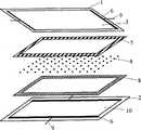
如图1所示,传统的四线电阻式触摸屏包括第一基层1和第二基层2,其中第一基层1通常为薄膜,第二基层2通常为玻璃或硬塑料平板,在第一基层1和第二基层2彼此相对的表面上分别涂有例如为透明的氧化铟锡(ITO)的导电物质,从而形成第一导电层3和第二导电层10。对于四线电阻式触摸屏,在第一导电层3和第二导电层10的一组对边上分别印刷有两条相对平行的电极6,即所谓的印刷电极,该电极6通常由银粉构成,且在各电极6上均通过电极引出线9与触摸屏控制器相连。此外,在第一导电层3和第二导电层10之间分别通过绝缘层8和隔离层4加以绝缘和隔离,且通过粘结层5连接第一基层1和第二基层2。As shown in Figure 1, a traditional four-wire resistive touch screen includes a
通过上述工艺制作出的四线电阻式触摸屏,虽具有良好的性能,但由于需要印刷电极、印刷绝缘层以及粘结电极引出线等步骤,使得产品的制作周期较长,生产成本及产品不良率也较高。Although the four-wire resistive touch screen produced by the above process has good performance, due to the need for printing electrodes, printing insulating layers, and bonding electrode lead-out steps, the production cycle of the product is longer, and the production cost and product defect rate are relatively long. Also higher.
发明内容Contents of the invention
为了克服现有的四线电阻式触摸屏的制作工艺复杂、制作周期长等问题,本发明提供一种制作工艺简单并可显著缩短制作周期的新型的四线电阻式触摸屏及其制作方法。In order to overcome the problems of complex manufacturing process and long manufacturing cycle of the existing four-wire resistive touch screen, the present invention provides a novel four-wire resistive touch screen and its manufacturing method with simple manufacturing process and significantly shortened manufacturing cycle.
本发明提供一种四线电阻式触摸屏,该四线电阻式触摸屏包括第一基层、第二基层、第一导电层、第二导电层、隔离层、至少四个电极以及至少四个电极引出线,第一基层和第二基层平行地相对放置,第一导电层和第二导电层分别覆盖在第一基层和第二基层彼此相对的面上,隔离层位于第一导电层或第二导电层上,至少四个电极中的至少两个电极位于第一导电层的相对的两边且相互平行,其余的电极位于第二导电层的相对的两边且相互平行,位于第一导电层的电极与位于第二导电层的电极相互垂直,每个电极分别连接一个电极引出线;其中,所述位于第一导电层的电极与所述第一导电层电连接并与第二导电层绝缘连接,所述位于第二导电层的电极与所述第一导电层绝缘连接并与所述第二导电层电连接,每个电极和与该电极相连的电极引出线为一块柔性印刷线路板。The present invention provides a four-wire resistive touch screen, which includes a first base layer, a second base layer, a first conductive layer, a second conductive layer, an isolation layer, at least four electrodes, and at least four electrode lead-out lines , the first base layer and the second base layer are placed opposite to each other in parallel, the first conductive layer and the second conductive layer are respectively covered on the opposite surfaces of the first base layer and the second base layer, and the isolation layer is located on the first conductive layer or the second conductive layer At least two of the at least four electrodes are located on opposite sides of the first conductive layer and parallel to each other, and the rest of the electrodes are located on opposite sides of the second conductive layer and parallel to each other. The electrodes of the second conductive layer are perpendicular to each other, and each electrode is respectively connected to an electrode lead-out line; wherein, the electrodes on the first conductive layer are electrically connected to the first conductive layer and insulatedly connected to the second conductive layer, and The electrodes on the second conductive layer are insulated and connected to the first conductive layer and electrically connected to the second conductive layer, and each electrode and the electrode lead wires connected to the electrodes are a flexible printed circuit board.
本发明还提供一种四线电阻式触摸屏的制作方法,其中,该方法包括以下步骤:在第一基层和第二基层的一个表面上分别形成第一导电层和第二导电层;在第一导电层或第二导电层上形成隔离层;将柔性印刷线路板切割成至少四个电极,且每个电极边缘上具有一个一体构造的电极引出线;将所述至少四个电极放置在第一导电层和第二导电层之间没有印刷隔离层的位置,使得该至少四个电极中的至少两个电极位于第一导电层的相对的两边且相互平行,其余的电极位于第二导电层的相对的两边且相互平行,位于第一导电层的电极与位于第二导电层的电极相互垂直;以及将所述位于第一导电层的电极与所述第一导电层电连接并与第二导电层绝缘连接,且将所述位于第二导电层的电极与所述第一导电层绝缘连接并与所述第二导电层电连接。The present invention also provides a method for manufacturing a four-wire resistive touch screen, wherein the method includes the following steps: respectively forming a first conductive layer and a second conductive layer on one surface of the first base layer and the second base layer; An isolation layer is formed on the conductive layer or the second conductive layer; the flexible printed circuit board is cut into at least four electrodes, and each electrode edge has an integrally constructed electrode lead-out line; the at least four electrodes are placed on the first There is no position for printing an isolation layer between the conductive layer and the second conductive layer, so that at least two electrodes in the at least four electrodes are located on opposite sides of the first conductive layer and are parallel to each other, and the remaining electrodes are located on the sides of the second conductive layer. The opposite sides are parallel to each other, the electrodes on the first conductive layer and the electrodes on the second conductive layer are perpendicular to each other; and the electrodes on the first conductive layer are electrically connected to the first conductive layer and connected to the second conductive layer The layer is insulated and connected, and the electrode located on the second conductive layer is insulated and connected to the first conductive layer and electrically connected to the second conductive layer.
通过上述制作方法制成的四线电阻式触摸屏保持了传统四线电阻式触摸屏的高分辨率等优点,同时在工艺方面,本发明提供的四线电阻式触摸屏采用柔性印刷线路板作为电极,该柔性印刷线路板可通过双面胶等常见的粘结物质固定于第一导电层和第二导电层之间,从而避免了繁琐的传统电极的印刷步骤。且由于柔性印刷线路板的外表面上本身具有绝缘层,因此在触摸屏的制作过程中省去了印刷绝缘层的步骤。此外,由于本发明中的电极引出线与电极是一体构造的,因而省略了在电极上粘结电极引出线的步骤。因此,与传统的四线电阻式触摸屏的制作工艺相比,本发明提供的四线电阻式触摸屏在反应电压分布均匀性情况的线性测试中,对触摸点位置的检测的平均误差低于1.5%的同时,制作工艺明显简化,由此使得产品具有成本低廉,制作周期短且产品不良率较低等优点。The four-wire resistive touch screen made by the above manufacturing method maintains the advantages of the traditional four-wire resistive touch screen such as high resolution. The flexible printed circuit board can be fixed between the first conductive layer and the second conductive layer by common adhesive substances such as double-sided tape, thereby avoiding the cumbersome traditional electrode printing steps. Moreover, since the outer surface of the flexible printed circuit board itself has an insulating layer, the step of printing the insulating layer is omitted during the manufacturing process of the touch screen. In addition, since the electrode lead-out wire and the electrode are integrally constructed in the present invention, the step of bonding the electrode lead-out wire to the electrode is omitted. Therefore, compared with the manufacturing process of the traditional four-wire resistive touch screen, the four-wire resistive touch screen provided by the present invention has an average error of less than 1.5% in the detection of the position of the touch point in the linear test of the response voltage distribution uniformity At the same time, the production process is obviously simplified, so that the product has the advantages of low cost, short production cycle and low product defect rate.
附图说明Description of drawings
图1是传统电阻式触摸屏的结构的示意图;FIG. 1 is a schematic diagram of the structure of a traditional resistive touch screen;
图2是根据本发明的一种实施方式的电阻式触摸屏的结构的侧视图;2 is a side view of the structure of a resistive touch screen according to an embodiment of the present invention;
图3是根据本发明的一种实施方式的电阻式触摸屏的电极分布示意图;3 is a schematic diagram of electrode distribution of a resistive touch screen according to an embodiment of the present invention;
图4是根据本发明的另一种实施方式的电阻式触摸屏的电极分布示意图。FIG. 4 is a schematic diagram of electrode distribution of a resistive touch screen according to another embodiment of the present invention.
具体实施方式Detailed ways
如图2所示,本发明提供一种四线电阻式触摸屏,该四线电阻式触摸屏包括第一基层1、第二基层2、第一导电层3、第二导电层10、隔离层4、至少四个电极6以及至少四个电极引出线9,第一基层1和第二基层2平行地相对放置,第一导电层3和第二导电层10分别覆盖在第一基层1和第二基层2彼此相对的面上,隔离层4位于第一导电层3或第二导电层10上,至少四个电极6中的至少两个电极6位于第一导电层3的相对的两边且相互平行,其余的电极6位于第二导电层10的相对的两边且相互平行,位于第一导电层3的电极6与位于第二导电层10的电极6相互垂直,每个电极6分别连接一个电极引出线9;其中,所述位于第一导电层3的电极6与所述第一导电层3电连接并与第二导电层10绝缘连接,所述位于第二导电层10的电极6与所述第一导电层3绝缘连接并与所述第二导电层10电连接,每个电极6和与该电极6相连的电极引出线9为一块柔性印刷线路板。As shown in Figure 2, the present invention provides a four-wire resistive touch screen, which includes a
如本领域技术人员所公知的,所述第一基层1可以为任意的具有透光性的薄膜,优选为采用透明聚脂膜。所述第二基层2可以为任意的具有透光性的平板,优选为采用厚度为1.0-3.0mm的玻璃板、硬塑料板或树脂板。所述第一导电层3和第二导电层10可以由任意的分别均匀涂覆在第一基层1和第二基层2上且具有透光性的导电物质构成,优选为采用氧化铟锡(ITO)构成。所述隔离层4可以由多个具有任意形状和间隔的透光性隔离物组成,以隔离涂覆在第一基层1和第二基层2上的第一导电层3和第二导电层10,例如,可采用如图1所示的柱状的点隔片阵列,为了防止触摸屏误操作,点隔片理论上越小越好,但是点隔片过小可能会影响触摸屏的控制,所以优选为采用尺寸为2mm×2mm-4mm×4mm的点隔片。电极引出线9为由柔性印刷线路板构造的电极6边缘上的一个凸起,该凸起可以被构造为任意形状且位于电极6外边缘上的任意位置。As known to those skilled in the art, the
所述柔性印刷线路板可以通过商购得到,该柔性印刷线路板包括基板和连续覆盖在基板表面的导电层,导电层的表面覆盖绝缘层,且覆盖在导电层表面的绝缘层具有暴露出导电层的部分,例如,表面具有焊盘结构的柔性印刷线路板。该柔性印刷线路板通过柔性印刷线路板表面上暴露出金属的部分与第一导电层3或第二导电层10电连接。The flexible printed circuit board can be obtained commercially. The flexible printed circuit board includes a substrate and a conductive layer continuously covering the surface of the substrate. The surface of the conductive layer is covered with an insulating layer, and the insulating layer covered on the surface of the conductive layer has exposed conductive layers. Part of the layer, for example, a flexible printed wiring board with a pad structure on its surface. The flexible printed circuit board is electrically connected to the first
所述四线电阻式触摸屏还包括粘结层5,该粘结层5分别位于所述柔性印刷线路板与第一导电层3和第二导电层10相对的面上,用于将所述柔性印刷线路板与第一导电层3或第二导电层10相连接,且位于所述柔性印刷线路板表面暴露出导电层的部分上的粘结层5由粘性导电材料构成。这样,所述柔性印刷线路板可以通过附着在所述暴露出导电层的位置上的粘结层5而与第一导电层3或第二导电层10电连接,而附着在该柔性印刷线路板其余位置上的部分可以为例如双面胶等绝缘粘性材料,由此,可进一步降低生产成本。The four-wire resistive touch screen also includes an
如图1所示,传统的电阻式触摸屏在第一导电层3和第二导电层10之间还具有一些印刷层,其中包括印刷于每个导电层的一组对边上的电极6以及印刷于该电极6上的绝缘层8,其中所述电极6通常由均匀印刷的银粉构成且可分别在两导电层中产生线性化电场。此外,为了将触摸屏与其控制器相连接,如图1所示,需要在所述各个电极6上通过粘结层5连接电极引出线9,以便通过电极引出线9与控制器相连。在传统的电阻式触摸屏中,所述电极引出线9通常与电极6分立构造,并通过粘结层5与电极6相连。As shown in Figure 1, a conventional resistive touch screen also has some printed layers between the first
本发明所述的电阻式触摸屏的电极6由柔性印刷线路板切割而成,从而代替了传统电极6的由银粉印刷而成的工艺,且所述由柔性印刷线路板切割成的电极6同样可以在触摸屏的第一导电层3和第二导电层10上分别产生均匀分布的电压场,且因为商购得到的柔性印刷线路板在其上的导电金属层表面上已经覆盖有绝缘层,因此,在触摸屏的制作过程中,可省去在电极表面印刷绝缘层的传统工艺,只需按照上述方法将柔性印刷线路板通过粘性导电材料与其对应的第一导电层3或第二导电层10粘结即可。此外,如图3所示,在将柔性印刷线路板剪裁为尺寸适当的电极6的同时,还可在每个电极6的边缘上切割出凸起以作为电极引出线9,从而使电极6和电极引出线9一体构造为一块柔性印刷线路板,由此省去了通过粘结层5粘结电极引出线9的传统工艺。The
此外,在使用柔性印刷线路板制作电极6时,可以使位于第一导电层3或第二导电层10不同边上的柔性印刷线路板独立构造,也可以使位于第一导电层3一边上的柔性印刷线路板和第二导电层10一边上的柔性印刷线路板为一块柔性印刷线路板,还可以使位于第一导电层3和第二导电层10上的所有柔性印刷线路板为一块柔性印刷线路板,且在这种情况下,相互平行的柔性印刷线路板之间为绝缘连接,这可以通过对柔性印刷线路板的导电层的蚀刻而实现。In addition, when using a flexible printed circuit board to make the
如图3和4所示,当位于第一导电层3和/或第二导电层10同一边上的柔性印刷线路板为多块时,只要满足电压场的线性化要求,同一边上的多块柔性印刷线路板之间的距离可随意变化,且柔性印刷线路板的数目也可以随意设定,优选情况下,同一边上被柔性印刷线路板覆盖的长度与相邻两块柔性印刷线路板之间的未被柔性印刷线路板覆盖的空隙长度之间的比值为1∶3至3∶1。在此种情况下,每块柔性印刷线路板均具有一个与该柔性印刷线路板一体构造的电极引出线9,且每个电极引出线9可以被单独供电,也可以将位于第一导电层3和/或第二导电层10同一边上的柔性印刷线路板各自的电极引出线9连接在一起后统一供电。为了保证所加电压的均匀性,优选为对所述位于同一边上的多个电极引出线9单独供电。As shown in Figures 3 and 4, when there are multiple flexible printed circuit boards on the same side of the first
本发明还提供一种四线电阻式触摸屏的制作方法,其中,该方法包括以下步骤:在第一基层1和第二基层2的一个表面上分别形成第一导电层3和第二导电层10;在第一导电层3或第二导电层10上形成隔离层4;将柔性印刷线路板切割成至少四个电极6,且每个电极6边缘上具有一个一体构造的电极引出线9;将所述至少四个电极6放置在第一导电层3和第二导电层10之间没有印刷隔离层4的位置,使得该至少四个电极6中的至少两个电极6位于第一导电层3的相对的两边且相互平行,其余的电极6位于第二导电层10的相对的两边且相互平行,位于第一导电层3的电极6与位于第二导电层10的电极6相互垂直;以及将所述位于第一导电层3的电极6与所述第一导电层3电连接并与第二导电层10绝缘连接,且将所述位于第二导电层10的电极6与所述第一导电层3绝缘连接并与所述第二导电层10电连接。The present invention also provides a method for manufacturing a four-wire resistive touch screen, wherein the method includes the following steps: forming a first
此外,在印刷隔离层4后,可将第一基层1和第二基层2切割成需要的尺寸。其中,先在第一基层1和第二基层2上分别制作第一导电层3、第二导电层10以及隔离层4,之后再对第一基层1和第二基层2进行切割是为了提高生产效率,因此,在生产数量不多的情况下,也可以先对第一基层1和第二基层2进行切割,之后再分别制作两个导电层和隔离层4。In addition, after the
如本领域技术人员所公知的,所述第一基层1可以为任意的具有透光性的薄膜,优选为采用透明聚脂膜。所述第二基层2可以为任意的具有透光性的平板,优选为采用厚度为1.0-3.0mm的玻璃板、硬塑料板或树脂板。所述第一导电层3和第二导电层10可以由任意的分别均匀涂覆在第一基层1和第二基层2上且具有透光性的导电物质构成,优选为采用氧化铟锡(ITO)构成。所述隔离层4可以由多个具有任意形状和间隔的透光性隔离物组成,以隔离涂覆在第一基层1和第二基层2上的第一导电层3和第二导电层10,例如,可采用如图1所示的柱状的点隔片阵列。位于第一导电层3和/或第二导电层10同一边上的柔性印刷线路板为多块,且同一边上被柔性印刷线路板覆盖的长度与相邻两块柔性印刷线路板之间的未被柔性印刷线路板覆盖的空隙长度之间的比值为1∶3至3∶1。电极引出线9为由柔性印刷线路板构造的电极6边缘上的一个凸起,该凸起可以被构造为任意形状且位于电极6外边缘上的任意位置。此外,所述第一导电层3和第二导电层10的电镀及隔离层4的印刷为本领域技术人员所公知的制作方法,在此不再赘述。As known to those skilled in the art, the
所述柔性印刷线路板可以通过商购得到,该柔性印刷线路板包括基板和连续覆盖在基板表面的导电层,导电层的表面覆盖绝缘层,且覆盖在导电层表面的绝缘层具有暴露出导电层的部分,例如,表面具有焊盘结构的柔性印刷线路板。该柔性印刷线路板通过柔性印刷线路板表面上暴露出金属的部分与第一导电层3或第二导电层10电连接。The flexible printed circuit board can be obtained commercially. The flexible printed circuit board includes a substrate and a conductive layer continuously covering the surface of the substrate. The surface of the conductive layer is covered with an insulating layer, and the insulating layer covered on the surface of the conductive layer has exposed conductive layers. Part of the layer, for example, a flexible printed wiring board with a pad structure on its surface. The flexible printed circuit board is electrically connected to the first
所述将所述位于第一导电层3的电极6与所述第一导电层3电连接并与第二导电层10绝缘连接,且将所述位于第二导电层10的电极6与所述第一导电层3绝缘连接并与所述第二导电层10电连接的步骤是通过分别在所述柔性印刷线路板与第一导电层3和第二导电层10相对的面上形成粘结层5,且使得位于该柔性印刷线路板表面暴露出导电层的部分上的粘结层5为粘性导电材料而实现的。例如,可在130℃-170℃的温度下,在第一导电层3或第二导电层10的一组对边上施加例如0.3mpa的压力,从而通过在所述电极6的一个表面暴露出导电层的部分上使用的例如异性导电胶(ACP)的粘性导电材料而将该柔性印刷线路板固定到第一导电层3或第二导电层10上,且为了最大限度地降低生产成本,优选为在该电极6的其余部分附着双面胶等粘性绝缘材料。由此使得电极6与第一导电层3和第二导电层10分别实现电连接和绝缘连接。The
此外,在使用柔性印刷线路板制作电极6时,可以使位于第一导电层3或第二导电层10不同边上的柔性印刷线路板独立构造,也可以使位于第一导电层3一边上的柔性印刷线路板和第二导电层10一边上的柔性印刷线路板为一体构造,还可以使位于第一导电层3和第二导电层10上的所有柔性印刷线路板为一体构造,且在这种情况下,相互平行的柔性印刷线路板之间为绝缘连接,这可以通过对柔性印刷线路板的导电层的蚀刻而实现。In addition, when using a flexible printed circuit board to make the
如图3和4所示,当位于第一导电层3和/或第二导电层10同一边上的柔性印刷线路板为多块时,只要满足电压场的线性化要求,同一边上的多块柔性印刷线路板之间的距离可随意变化,且柔性印刷线路板的数目也可以随意设定,优选情况下,同一边上被柔性印刷线路板覆盖的长度与相邻两块柔性印刷线路板之间的未被柔性印刷线路板覆盖的空隙长度之间的比值为1∶3至3∶1。在此种情况下,每块柔性印刷线路板均具有一个与该柔性印刷线路板一体构造的电极引出线9,且每个电极引出线9可以被单独供电,也可以将位于第一导电层3和/或第二导电层10同一边上的柔性印刷线路板各自的电极引出线9连接在一起后统一供电。为了保证所加电压的均匀性,优选为对所述位于同一边上的多个电极引出线9单独供电。As shown in Figures 3 and 4, when there are multiple flexible printed circuit boards on the same side of the first
由此,当触摸屏表面受到的压力(如通过笔尖或手指进行按压)足够大时,第一基层1与第二基层2之间会产生接触,第一基层1和第二基层2的电阻随之发生变化并在图4所示的X和Y两个方向上产生相应的信号,该信号通过电极引出线9传送到控制器,控制器由此计算出触摸点的X和Y两个方向上的坐标。触摸屏计算触摸点坐标所用的分压器原理为本领域技术人员所公知,在此不再赘述。Thus, when the pressure on the surface of the touch screen (such as pressing by a pen tip or a finger) is large enough, contact will be generated between the
Claims (11)
Priority Applications (1)
| Application Number | Priority Date | Filing Date | Title |
|---|---|---|---|
| CN2008100978574ACN101587410B (en) | 2008-05-19 | 2008-05-19 | Four-wire resistance type touch screen and manufacturing method thereof |
Applications Claiming Priority (1)
| Application Number | Priority Date | Filing Date | Title |
|---|---|---|---|
| CN2008100978574ACN101587410B (en) | 2008-05-19 | 2008-05-19 | Four-wire resistance type touch screen and manufacturing method thereof |
Publications (2)
| Publication Number | Publication Date |
|---|---|
| CN101587410A CN101587410A (en) | 2009-11-25 |
| CN101587410Btrue CN101587410B (en) | 2011-05-18 |
Family
ID=41371674
Family Applications (1)
| Application Number | Title | Priority Date | Filing Date |
|---|---|---|---|
| CN2008100978574AExpired - Fee RelatedCN101587410B (en) | 2008-05-19 | 2008-05-19 | Four-wire resistance type touch screen and manufacturing method thereof |
Country Status (1)
| Country | Link |
|---|---|
| CN (1) | CN101587410B (en) |
Families Citing this family (5)
| Publication number | Priority date | Publication date | Assignee | Title |
|---|---|---|---|---|
| CN101825796B (en) | 2010-05-19 | 2012-06-13 | 北京富纳特创新科技有限公司 | Touch liquid crystal screen |
| CN101852934A (en) | 2010-05-31 | 2010-10-06 | 北京富纳特创新科技有限公司 | Touch type liquid crystal display screen |
| CN101852935A (en) | 2010-06-02 | 2010-10-06 | 北京富纳特创新科技有限公司 | Touch liquid crystal display |
| CN101990017B (en)* | 2010-09-29 | 2013-08-14 | 惠州Tcl移动通信有限公司 | Mobile phone device and realization method thereof |
| CN111857415B (en)* | 2020-07-01 | 2024-02-27 | 清华大学深圳国际研究生院 | Multi-point type resistance touch screen and addressing method |
Citations (2)
| Publication number | Priority date | Publication date | Assignee | Title |
|---|---|---|---|---|
| US6549193B1 (en)* | 1998-10-09 | 2003-04-15 | 3M Innovative Properties Company | Touch panel with improved linear response and minimal border width electrode pattern |
| CN1438608A (en)* | 2003-03-18 | 2003-08-27 | 中国电子科技集团公司第五十五研究所 | Periphery electrode width changeable contact screen |
- 2008
- 2008-05-19CNCN2008100978574Apatent/CN101587410B/ennot_activeExpired - Fee Related
Patent Citations (2)
| Publication number | Priority date | Publication date | Assignee | Title |
|---|---|---|---|---|
| US6549193B1 (en)* | 1998-10-09 | 2003-04-15 | 3M Innovative Properties Company | Touch panel with improved linear response and minimal border width electrode pattern |
| CN1438608A (en)* | 2003-03-18 | 2003-08-27 | 中国电子科技集团公司第五十五研究所 | Periphery electrode width changeable contact screen |
Also Published As
| Publication number | Publication date |
|---|---|
| CN101587410A (en) | 2009-11-25 |
Similar Documents
| Publication | Publication Date | Title |
|---|---|---|
| TWI426427B (en) | Touch panel | |
| CN100541403C (en) | Panel input device | |
| TW201706803A (en) | Touch 3D-signal input equipment and multi-function touch panel | |
| CN102081479A (en) | Touch display panel and touch panel | |
| CN101587410B (en) | Four-wire resistance type touch screen and manufacturing method thereof | |
| US11163415B2 (en) | Touch display module, touch display device and electronic device | |
| CN103970312A (en) | Touch display device | |
| CN102221919A (en) | Touch panel | |
| JP2018036973A (en) | Method for acquiring data from resistance film type touch panel, and resistance film type touch panel device | |
| CN204719367U (en) | A kind of display panels and display device | |
| CN109271062B (en) | Driving circuit and driving method thereof, touch device and working method thereof | |
| CN106201040A (en) | The manufacture method of touch screen, display device and touch screen | |
| CN206805509U (en) | Contact panel and display device | |
| CN216249201U (en) | Capacitive electromagnetic touch module, touch screen and electronic equipment | |
| CN201725303U (en) | Matrix touch panel | |
| CN110362240B (en) | Capacitive screen and terminal device with channel switching function | |
| CN204595807U (en) | Touch-screen and display device | |
| CN104063079B (en) | Electrode bridging structure of touch panel | |
| CN104777684B (en) | Self-capacitance touch liquid crystal grating and preparation method thereof, display screen, display device | |
| CN212586859U (en) | Capacitive touch screen | |
| CN204044782U (en) | Touch screen and touch device | |
| CN207663432U (en) | Improved signal bus connecting structure of touch control board | |
| CN102890589B (en) | Conductive pattern structure and construction method of capacitive touch panel | |
| CN110321032B (en) | Display panel and display device | |
| CN111522467A (en) | Touch panel, preparation method thereof and touch panel assembly |
Legal Events
| Date | Code | Title | Description |
|---|---|---|---|
| C06 | Publication | ||
| PB01 | Publication | ||
| C10 | Entry into substantive examination | ||
| SE01 | Entry into force of request for substantive examination | ||
| C14 | Grant of patent or utility model | ||
| GR01 | Patent grant | ||
| ASS | Succession or assignment of patent right | Owner name:SHENZHEN BYD ELECTRONIC COMPONENT CO., LTD. Free format text:FORMER OWNER: BIYADI CO., LTD. Effective date:20150906 | |
| C41 | Transfer of patent application or patent right or utility model | ||
| TR01 | Transfer of patent right | Effective date of registration:20150906 Address after:518118 Byd Co experimental building, 1 Yanan Road, Kwai Chung Town, Dapeng District, Guangdong, Shenzhen Patentee after:SHENZHEN BYD ELECTRONIC COMPONENT Co.,Ltd. Address before:518118, Ping Ping Road, Pingshan Town, Longgang District, Guangdong, Shenzhen 3001 Patentee before:BYD Co.,Ltd. | |
| CP01 | Change in the name or title of a patent holder | ||
| CP01 | Change in the name or title of a patent holder | Address after:518118 Byd Co experimental building, 1 Yanan Road, Kwai Chung Town, Dapeng District, Guangdong, Shenzhen Patentee after:Shenzhen helitai photoelectric Co.,Ltd. Address before:518118 Byd Co experimental building, 1 Yanan Road, Kwai Chung Town, Dapeng District, Guangdong, Shenzhen Patentee before:SHENZHEN BYD ELECTRONIC COMPONENT Co.,Ltd. | |
| CF01 | Termination of patent right due to non-payment of annual fee | Granted publication date:20110518 | |
| CF01 | Termination of patent right due to non-payment of annual fee |